

Philips blv862 DATASHEETS
DISCRETE SEMICONDUCTORS
DATA SH EET
M3D091
BLV862
UHF linear push-pull power
transistor
Product specification
Supersedes data of 1997 Oct 14
1999 Jun 25
Philips Semiconductors Product specification
UHF linear push-pull power transistor BLV862
FEATURES
• Double stage internal input and output matching
networks for an optimum wideband capability and
high gain
• Polysilicon emitter ballasting resistors for an optimum
temperature profile
• Gold metallization ensures excellent reliability.
APPLICATIONS
• Common emitter class-AB operation in output stages in
bands 4 and 5 (470 to 860 MHz) television transmitter
amplifiers (vision or sound).
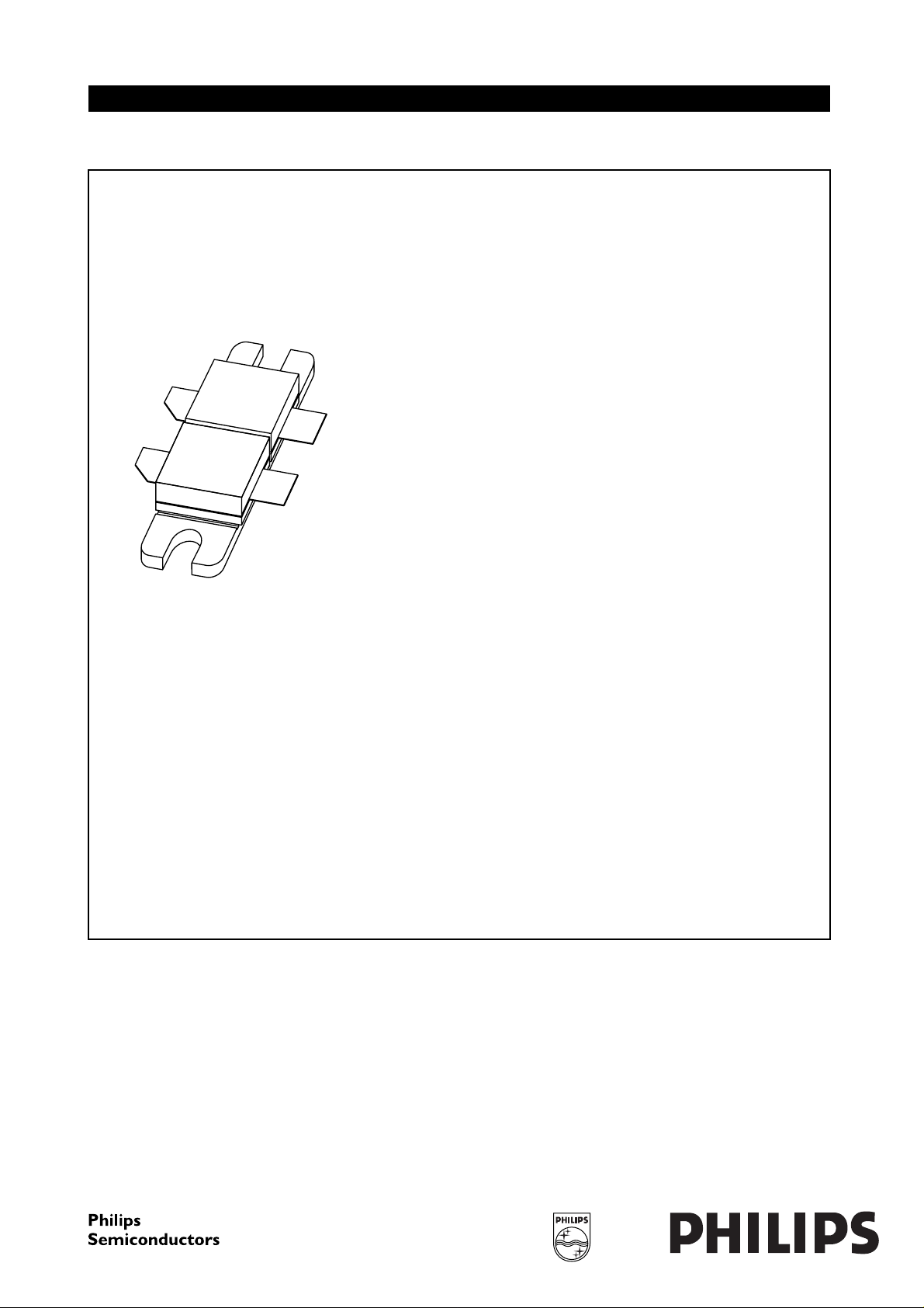
DESCRIPTION
NPN silicon planar epitaxial transistor with two sections in
push-pull configuration. The device is encapsulated in a
SOT262B 4-lead rectangular flange package, with two
ceramic caps.
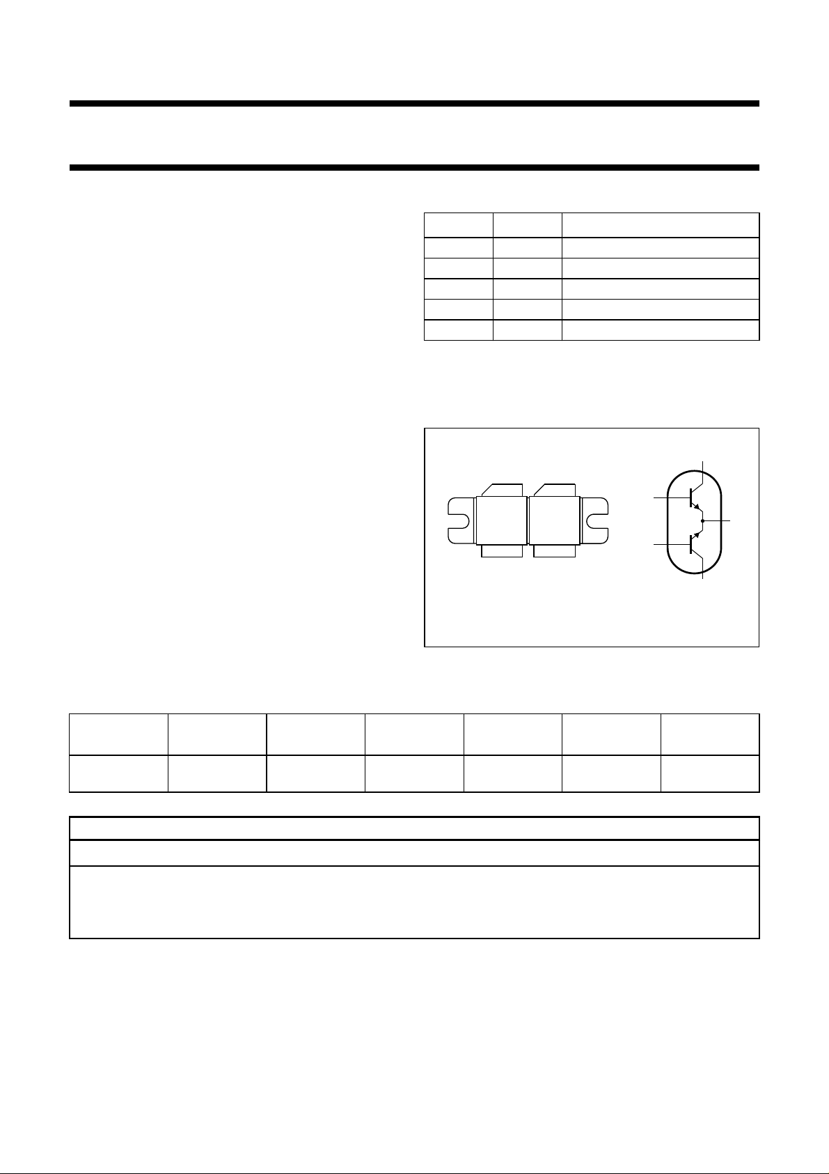
PINNING
PIN SYMBOL DESCRIPTION
1 c1 collector 1; note 1
2 c2 collector 2; note 1
3 b1 base 1
4 b2 base 2
5 e common emitter; note 2
Notes
1. Collectors 1 and 2 are connected together internally.
2. Common emitters are connected to the flange.
handbook, halfpage
12
b1
55
34
Top view
b2
MAM031
c1
e
c2
Fig.1 Simplified outline (SOT262B) and symbol.
QUICK REFERENCE DATA
RF performance at T
MODE OF
OPERATION
CW class-AB 860 28 150
=25°C in a common emitter push-pull test circuit.
h
f
(MHz)
V
(V)
CE
P
(W)
L
G
p
(dB)
≥8
typ. 9
η
C
(%)
≥45
typ. 52
∆G
(dB)
≤1
p
WARNING
Product and environmental safety - toxic materials
This product contains beryllium oxide. The product is entirely safe provided that the BeO discs are not damaged.
All persons who handle, use or dispose of this product should be aware of its nature and of the necessary safety
precautions. After use, dispose of as chemical or special waste according to the regulations applying at the location of
the user. It must never be thrown out with the general or domestic waste.
1999 Jun 25 2
Philips Semiconductors Product specification
UHF linear push-pull power transistor BLV862
LIMITING VALUES
In accordance with the Absolute Maximum Rating System (IEC 134).
SYMBOL PARAMETER CONDITIONS MIN. MAX. UNIT
V
CBO
V
CEO
V
EBO
I
C
P
tot
T
stg
T
j
THERMAL CHARACTERISTICS
SYMBOL PARAMETER CONDITIONS VALUE UNIT
R
th j-mb
R
th mb-h
collector-base voltage open emitter − 65 V
collector-emitter voltage open base − 30 V
emitter-base voltage open collector − 3V
collector current (DC) − 25 A
total power dissipation Tmb=25°C − 350 W
storage temperature −65 +150 °C
operating junction temperature − 200 °C
thermal resistance from junction to mounting base P
= 350 W; note 1 0.5 K/W
tot
thermal resistance from mounting base to heatsink note 1 0.15 K/W
Note
1. Thermal resistance is determined under specified RF operating conditions.
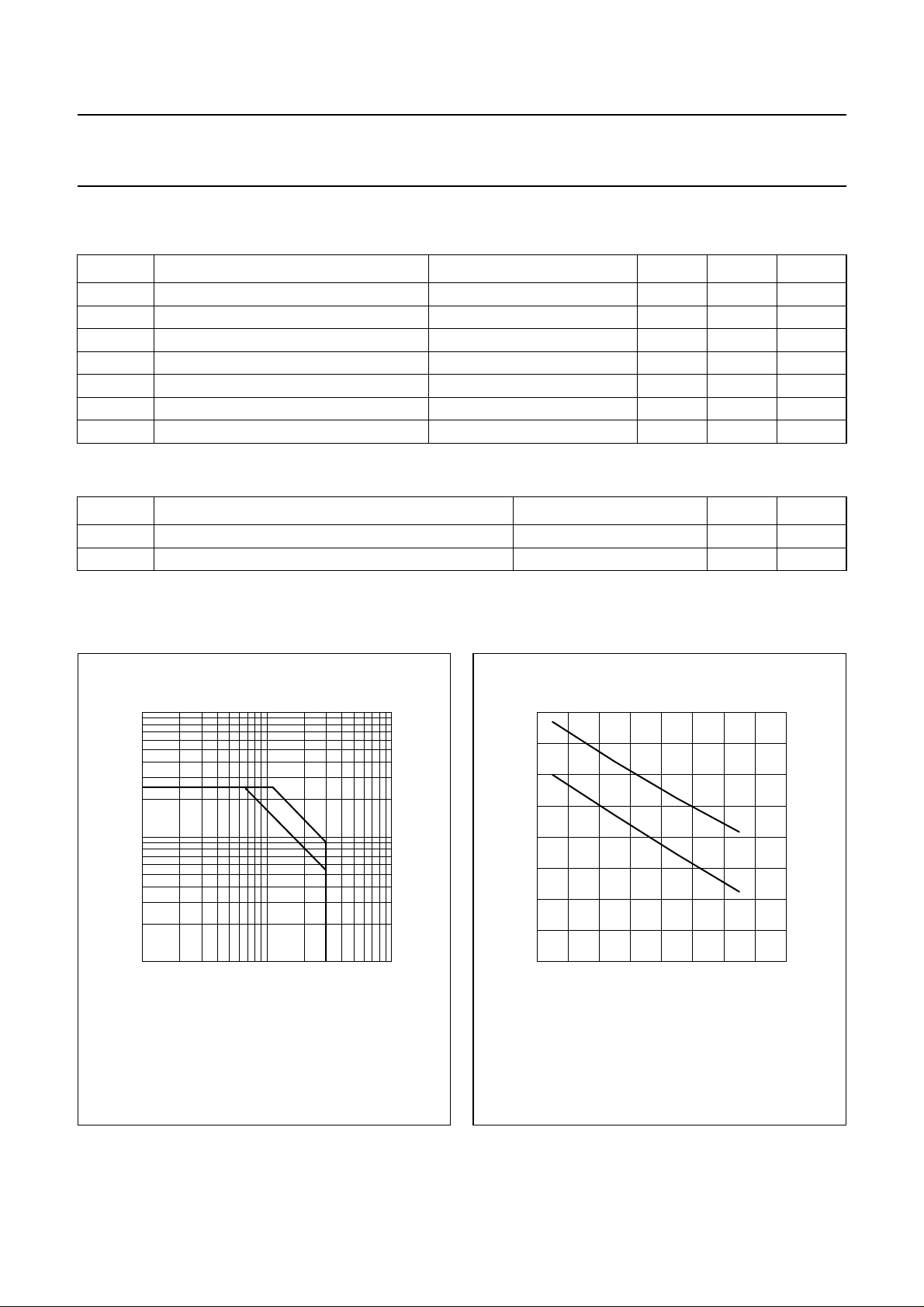
2
10
handbook, halfpage
I
C
(A)
10
1
11010
Total device; both sections equally loaded.
(1) Tmb=25°C.
(2) Th=70°C.
(1)
(2)
MBK231
V
(V)
CE
2
400
handbook, halfpage
P
tot
(W)
300
200
100
0
0 40 80 160
Total device; both sections equally loaded.
(1) Continuous operation.
(2) Short time operation during mismatch.
MGD528
(2)
(1)
120
Th (°C)
Fig.2 DC SOAR.
1999 Jun 25 3
Fig.3 Power derating curves.
Philips Semiconductors Product specification
UHF linear push-pull power transistor BLV862
CHARACTERISTICS
Values apply to either transistor section; T
SYMBOL PARAMETER CONDITIONS MIN. TYP. MAX. UNIT
V
(BR)CBO
V
(BR)CEO
V
(BR)EBO
I
CBO
h
FE
∆h
FE
C
c
collector-base breakdown voltage IE= 0; IC=60mA 65 −−V
collector-emitter breakdown voltage IB= 0; IC= 150 mA 30 −−V
emitter-base breakdown voltage IE= 3 mA; IC=0 3 −−V
collector-base leakage current VCB=28V −−5mA
DC current gain IC= 4.5 A; VCE=10V 30 − 140 −
DC current gain ratio of both sections IC= 4.5 A; VCE= 10 V 0.67 − 1.5 −
collector capacitance IE=ie= 0; VCE=28V;
Note
1. The value of C
is that of the die only, it is not measurable because of the internal matching network.
c
=25°C unless otherwise specified.
j
f = 1 MHz; note 1
− 75 − pF
APPLICATION INFORMATION
RF performance at T
MODE OF OPERATION
CW class-AB 860 28 0.8 150
=25°C in a common emitter push-pull class-AB test circuit; note 1.
h
f
(MHz)
V
(V)
CE
I
CQ
(A)
P
(W)
L
(dB)
typ. 9
G
≥8
p
η
C
(%)
≥45
typ. 52
∆G
(dB)
≤1
p
Note
1. See application note
“AN98014 in handbook SC19b
.”
Ruggedness in class-AB operation
The BLV862 is capable of withstanding a load mismatch corresponding to VSWR =2:1 through all phases under the
conditions: T
=25°C; f = 860 MHz; VCE= 28 V; ICQ= 0.8 A; PL= 150 W; R
h
th mb-h
= 0.15 K/W.
1999 Jun 25 4
 Loading...