

Philips BLV58 Datasheet

DISCRETE SEMICONDUCTORS
DATA SH EET
BLV58
UHF linear push-pull power
transistor
Product specification
September 1991
Philips Semiconductors Product specification
UHF linear push-pull power transistor BLV58
FEATURES
• High power gain
• Double stage internal input
matching for high input impedance
• Diffused emitter-ballasting resistors
enhances ruggedness
• Gold metallization for high
reliability.
DESCRIPTION
The BLV58 is a common emitter
epitaxial npn silicon planar transistor
designed for high linearity class-A
operation in UHF (bands 4 and 5) TV
transmitters and transposers.
The device is incorporated in a
push-pull SOT289 flange envelope
with a ceramic cap, which is utilized
with the emitters connected to the
flange.
PINNING - SOT289
QUICK REFERENCE DATA
RF performance at T
MODE OF
OPERATION
= 25 °C in a common emitter test circuit.
h
f
vision
(MHz)
V
(V)
CE
I
CQ
(A)
P
o sync
(W)
G
(dB)
p
d
(dB)
(note 1)
c.w. class-A 860 25 2 × 1.6 25 >10 <−45
Note
1. Three-tone test method (vision carrier −8 dB, sound carrier −7 dB,
sideband signal −16 dB); zero dB corresponds to peak sync level.
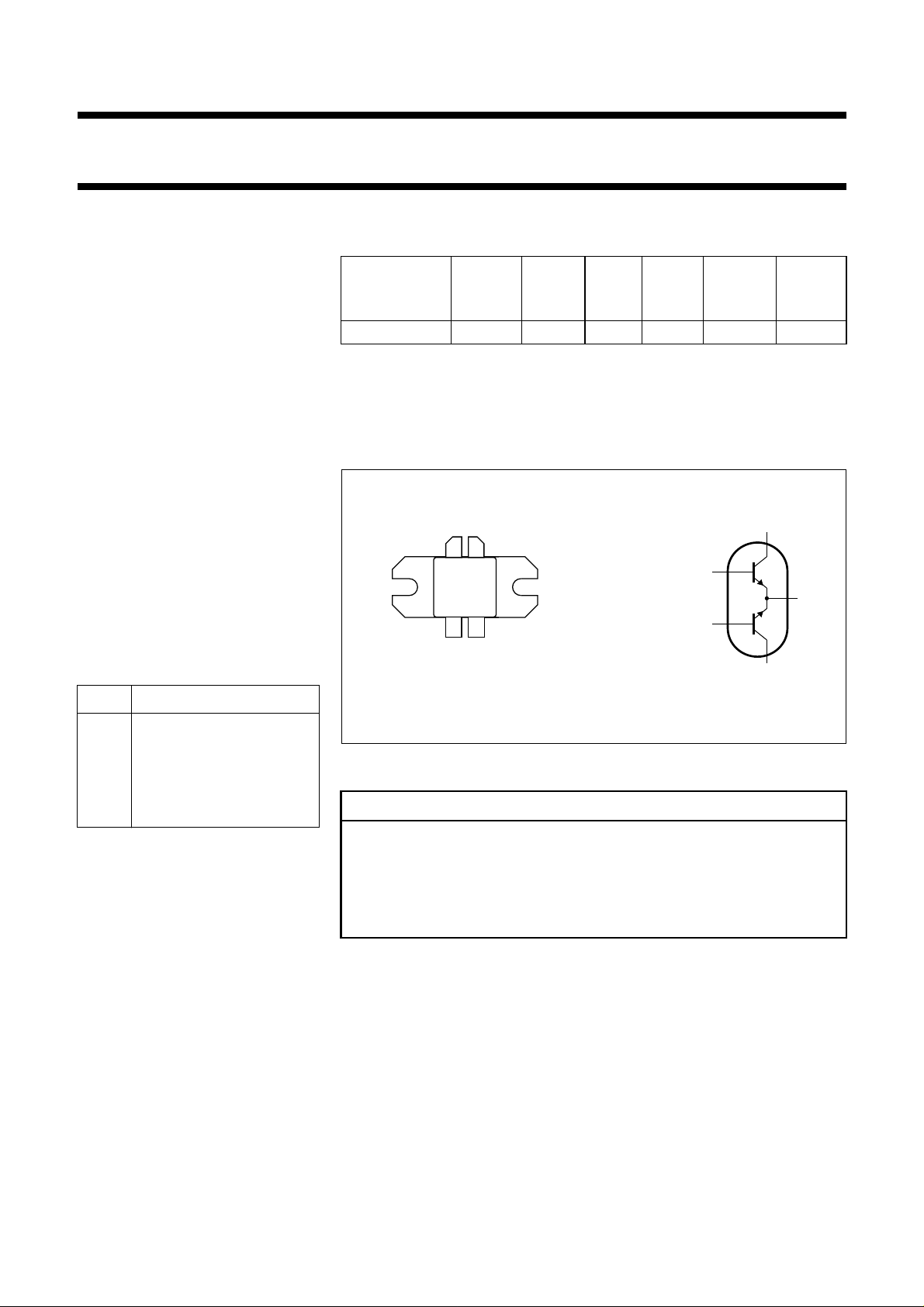
PIN CONFIGURATION
c1
, halfpage
12
34
Top view
5
MBC043
handbook, halfpage
b1
b2
MBA970
e
c2
im
PIN DESCRIPTION
1 collector 1
2 collector 2
3 base 1
4 base 2
5 emitter
Fig.1 Simplified outline and symbol.
WARNING
Product and environmental safety - toxic materials
This product contains beryllium oxide. The product is entirely safe provided
that the BeO discs are not damaged. All persons who handle, use or dispose
of this product should be aware of its nature and of the necessary safety
precautions. After use, dispose of as chemical or special waste according to
the regulations applying at the location of the user. It must never be thrown
out with the general or domestic waste.
September 1991 2
Philips Semiconductors Product specification
UHF linear push-pull power transistor BLV58
LIMITING VALUES (per transistor section unless otherwise specified)
In accordance with the Absolute Maximum System (IEC 134).
SYMBOL PARAMETER CONDITIONS MIN. MAX. UNIT
V
CBO
V
CEO
V
EBO
I
C,IC(AV)
I
CM
P
tot
T
stg
T
j
Note
1. Total device, both sections equally loaded.
collector-base voltage open emitter − 50 V
collector-emitter voltage open base − 27 V
emitter-base voltage open collector − 3.5 V
collector current DC or average value − 4A
collector current peak value;
− 8A
f > 1 MHz
total power dissipation DC operation;
− 87 W
Tmb=70°C
(note 1)
storage temperature range −65 150 °C
junction operating temperature − 200 °C
10
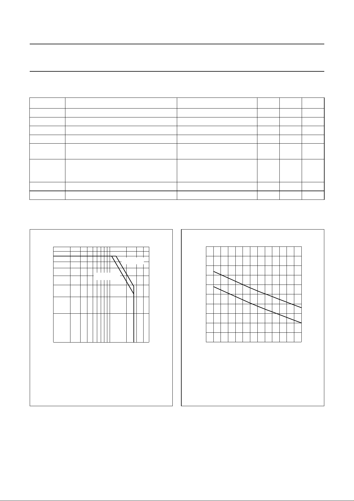
handbook, halfpage
I
C
(A)
T = 70 C
mb
1
110
Total device, both sections equally loaded.
Fig.2 DC SOAR.
o
T
= 25
h
C
V (V)
CE
MRA354
o
200
handbook, halfpage
P
tot
(W)
160
120
80
40
0
50
0 20 40 60 80 100 120
(I) Continuous DC operation.
(II) Short time operation during mismatch.
Total device, both sections equally loaded.
II
I
MRA355
T
h
o
( C)
Fig.3 Power derating curve.
September 1991 3

Philips Semiconductors Product specification
UHF linear push-pull power transistor BLV58
THERMAL RESISTANCE
SYMBOL PARAMETER CONDITIONS MAX. UNIT
R
th j-mb(DC)
R
th mb-h
from junction to mounting base P
from mounting base to heatsink note 1 0.2 K/W
Note
1. Total device, both sections equally loaded.
CHARACTERISTICS
Values apply to either transistor section; T
= 25 °C.
j
SYMBOL PARAMETER CONDITIONS MIN. TYP. MAX. UNIT
V
(BR)CBO
collector-base breakdown voltage open emitter;
IC=20mA
V
(BR)CEO
collector-emitter breakdown voltage open base;
IC=50mA
V
(BR)EBO
emitter-base breakdown voltage open collector;
IE=10mA
I
CES
collector-emitter leakage current VBE=0;
VCE=27V
h
FE
DC current gain VCE=25V;
IC= 1.6 A
C
c
collector capacitance VCB=25V;
IE=Ie=0;
f=1MHz
=87W;
dis
Tmb=70°C
(note 1)
1.5 K/W
50 −− V
27 −− V
3.5 −− V
−−10 mA
30 −−
− 36 45 pF
September 1991 4
 Loading...