

Philips BLV33 Datasheet

DISCRETE SEMICONDUCTORS
DATA SH EET
BLV33
VHF linear power transistor
Product specification
Supersedes data of November 1995
1996 Oct 10

Philips Semiconductors Product specification
VHF linear power transistor BLV33
FEATURES
• Diffused emitter ballasting resistors for an optimum
temperature profile
• Gold sandwich metallization ensures excellent
reliability.
APPLICATIONS
• Primarily intended for use in linear VHF amplifiers for
television transmitters and transposers.
DESCRIPTION
NPN silicon planar epitaxial transistor encapsulated in a
1
⁄16" 4 fslead SOT147 capstan package with ceramic cap.
All leads are isolated from the stud.
PINNING - SOT147
PIN SYMBOL DESCRIPTION
1 c collector
2 e emitter
3 b base
4 e emitter
handbook, halfpage
Top view
2
1
3
4
MAM270
Fig.1 Simplified outline and symbol.
c
b
e
QUICK REFERENCE DATA
RF performance in a common emitter push-pull test circuit.
MODE OF
OPERATION
f
vision
(MHz)
V
(V)
CE
IC, I
(A)
CW, class-A 224.25 25 3.2
C(ZS)
T
(°C)
(1)
h
d
im
(dB)
P
o sync
(W)
(1)
G
(dB)
70 −55 >16.5 >9
25 −55 typ. 26 typ. 9.7
P
sync compr.
sync in/sync out
(%)
(2)
CW, class-AB 224.25 28 0.1 70 typ. 90 typ. 6.5 30/25
Notes
1. Three-tone test method (vision carrier −8 dB, sound carrier −7 dB, sideband signal−16 dB), zero dB corresponds to
peak sync level.
2. Television service (negative modulation, C.C.I.R. system).
WARNING
Product and environmental safety - toxic materials
This product contains beryllium oxide. The product is entirely safe provided that the BeO disc is not damaged.
All persons who handle, use or dispose of this product should be aware of its nature and of the necessary safety
precautions. After use, dispose of as chemical or special waste according to the regulations applying at the location of
the user. It must never be thrown out with the general or domestic waste.
1996 Oct 10 2

Philips Semiconductors Product specification
VHF linear power transistor BLV33
LIMITING VALUES
In accordance with the Absolute Maximum Rating System (IEC 134).
SYMBOL PARAMETER CONDITIONS MIN. MAX. UNIT
V
CESM
V
CEO
V
EBO
I
C
I
C(AV)
I
CM
P
tot
P
rf
T
stg
T
j
THERMAL CHARACTERISTICS
collector-emitter voltage VBE=0 − 65 V
collector-emitter voltage open base − 33 V
emitter-base voltage open collector − 4V
collector current (DC) − 12.5 A
average collector current − 12.5 A
peak collector current f > 1 MHz − 20 A
total power dissipation (DC) Tmb=25°C − 132 W
RF power dissipation f > 1 MHz; Tmb=25°C − 165 W
storage temperature −65 +150 °C
operating junction temperature − 200 °C
SYMBOL PARAMETER CONDITIONS VALUE UNIT
R
th j-mb(dc)
thermal resistance from junction to
P
=80W; Tmb=82°C; Th=70°C 1.46 K/W
diss
mounting base (DC dissipation)
R
th j-mb(rf)
thermal resistance from junction to
P
=80W; Tmb=82°C; Th=70°C 1.17 K/W
diss
mounting base (RF dissipation)
R
th mb-h
thermal resistance from mounting
P
=80W; Tmb=82°C; Th=70°C 0.15 K/W
diss
base to heatsink
2
10
handbook, halfpage
I
C
(A)
10
1
11010
(1)
(3)
(2)
V
(V)
CE
MGG120
2
200
handbook, halfpage
P
tot
(W)
150
100
50
0 10050
(2)
(1)
MGG119
Th (°C)
(1) Tmb=25°C.
(2) Th=70°C.
(3) Second breakdown limit (independent of temperature).
Fig.2 DC SOAR.
1996 Oct 10 3
(1) Continuous DC (including RF class-A) operation.
(2) Continuous RF operation.
Fig.3 Power derating curves.

Philips Semiconductors Product specification
VHF linear power transistor BLV33
2.0
handbook, full pagewidth
R
th j-h
(K/W)
1.8
1.6
1.4
1.2
1.0
0
R
= 0.15 K/W.
th mb-h
75 °C
= 120 °C
T
h
100 °C
125 °C
10050
100 °C
150 °C
80 °C
P
tot
175 °C
(W)
MGG121
60 °C
40 °C
20 °C
0 °C
Tj = 200 °C
Fig.4 Maximum thermal resistance from junction to heatsink as a function of power dissipation, with heatsink
and junction temperature as parameters.
150
Example
Nominal class-A operation: VCE= 25 V; IC= 3.2 A; Th=70°C.
Figure 4 shows:
R
= max. 1.60 K/W
th j-h
Tj= max. 198 °C.
Typical device:
R
= typ.1.50 K/W
th j-h
Tj= typ. 190 °C.
1996 Oct 10 4

Philips Semiconductors Product specification
VHF linear power transistor BLV33
CHARACTERISTICS
T
=25°C; unless otherwise specified.
j
SYMBOL PARAMETER CONDITIONS MIN. TYP. MAX. UNIT
V
(BR)CES
V
(BR)CEO
V
(BR)EBO
I
CES
h
FE
V
CEsat
f
T
C
c
C
re
C
cs
collector-emitter breakdown voltage VBE= 0; IC=25mA 65 −−V
collector-emitter breakdown voltage open base; IC= 100 mA 33 −−V
emitter-base breakdown voltage open collector; IE=10mA 4 −−V
collector cut-off current VBE= 0; VCE=30V −−1mA
DC current gain VCE=25V; IC= 3 A; note 1 15 50 100
collector-emitter saturation voltage IC= 6 A; IB= 0.6 A; note 1 − 0.75 − V
transition frequency VCB=25V;IE=−3A;
− 680 − MHz
f = 100 MHz; note 2
transition frequency V
=25V;IE=−6A;
CB
− 750 − MHz
f = 100 MHz; note 2
collector capacitance VCB=25V; IE=ie= 0; f = 1 MHz − 155 − pF
feedback capacitance IC= 100 mA; VCE=25V;
− 88 − pF
f = 1 MHz
collector-stud capacitance − 3 − pF
Notes
1. Measured under pulse conditions: t
≤ 300 µs; δ≤0.02.
p
2. Measured under pulse conditions: tp≤ 50 µs; δ≤0.01.
1996 Oct 10 5
Philips Semiconductors Product specification
VHF linear power transistor BLV33
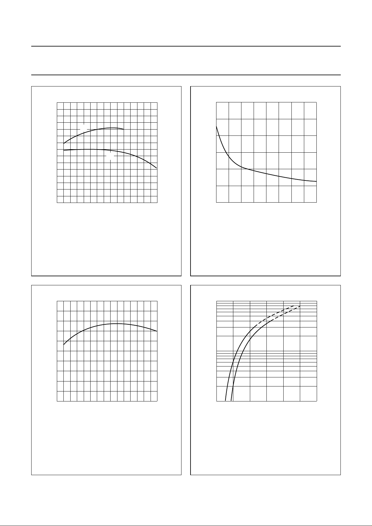
75
handbook, halfpage
h
FE
50
25
0
05 15
Tj=25°C.
(1) VCE=25V.
(2) VCE=5V.
(1)
(2)
10
MGG130
IC (A)
Fig.5 DC current gain as a function of collector
current; typical values.
600
handbook, halfpage
C
c
(pF)
400
200
0
02040
IE=ie= 0; f = 1 MHz; Tj=25°C.
VCB (V)
Fig.6 Collector capacitance as a function of
collector-base voltage; typical values.
MGG129
1000
handbook, halfpage
f
T
(MHz)
800
600
400
200
0
−0 −5 −15
VCB= 25 V; f = 100 MHz; Tj=25°C.
−10
MGG131
IE (A)
Fig.7 Transition frequency as a function of emitter
current; typical values.
10
handbook, halfpage
I
C
(A)
1
−1
10
VCE=25V.
(1) Th=70°C.
(2) Th=25°C.
(1)
(2)
Fig.8 Collector current as a function of
base-emitter voltage; typical values.
MGG118
VBE (V)
20.5 1 1.5
1996 Oct 10 6
 Loading...