

Philips blv2048 DATASHEETS
DISCRETE SEMICONDUCTORS
DATA SH EET
M3D374
BLV2048
UHF push-pull power transisto r
Preliminary specification
1999 Apr 23
Philips Semiconductors Preliminary specification
UHF push-pull power transistor BLV2048
FEATURES
• Emitter ballasting resistors for optimum temperature
profile
• Gold metallization ensures excellent reliability
• Internal input and output matc hing fo r an easy design of
wideband circuits.
• AlN substrate package for environmental safety
• Linear amplification with low distortion
• Low spectral regrowth in multichannel power amplifiers
according to IS-95.
APPLICATIONS
• Common emitter class-AB operati on in base stations for
PCN (Personal Communication Network): 1805 1880 MHz and PCS (Personal Communication
Services): 1910 - 1990 MHz.
DESCRIPTION
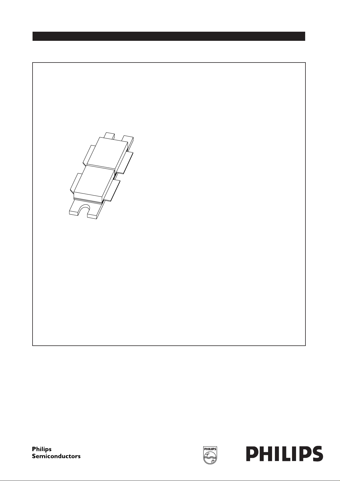
NPN silicon planar push-pull power transistor in a 4-lead
AIN SOT494A flange package with two ceramic caps.
The emitters are connected to the flange.
PINNING - SOT494A
PIN SYMBOL DESCRIPTION
1 c collector 1
2 c collector 2
3 b base 1
4 b base 2
5 e emitter, connected to flange
ook, halfpage
1
3
Top view
2
4
MBK202
Fig.1 Simplified outline.
5
QUICK REFERENCE DATA
RF performance at T
MODE OF
OPERATION
=25°C in a common emitter test circuit.
h
f
(MHz)
V
(V)
CE
P
(W)
L
G
p
(dB)
η
(%)
C
d
(dBc)
CW, class-AB 2000 26 120 ≥8 ≥40 −
2-tone, class-AB f
= 2000.0; f2= 2000.1 26 120 (PEP) ≥8.5 ≥33 ≤−28
1
LIMITING VALUES
In accordance with the Absolute Maximum Rating System (IEC 134)
Per section unless otherwise specified.
SYMBOL PARAMETER CONDITIONS MIN. MAX. UNIT
V
CBO
V
CEO
V
EBO
I
C
I
C(AV)
P
tot
T
stg
T
j
collector-base voltage open emitter − 65 V
collector-emitter voltage open base − 27 V
emitter-base voltage open collector − 3V
collector current (DC) − 20 A
average collector current − 10 A
total power dissipation Tmb=25°C − 415 W
storage temperature −65 +150 °C
operating junction temperature − 200 °C
im
1999 Apr 23 2

Philips Semiconductors Preliminary specification
UHF push-pull power transistor BLV2048
THERMAL CHARACTERISTICS
SYMBOL PARAMETER CONDITIONS VALUE UNIT
R
th j-h
R
th mb-h
Note
1. Thermal resistance is determined under nominal 2-tone RF operating conditions.
CHARACTERISTICS
T
=25°C; per section; unless otherwise specified.
j
SYMBOL PARAMETER CONDITIONS MIN. TYP. MAX. UNIT
V
(BR)CBO
V
(BR)CEO
V
(BR)EBO
I
CES
h
FE
C
c
C
re
thermal resistance from junction to
heatsink
thermal resistance from mounting
PL= 120 W(PEP); Th=40°C; note 1:
total device; both sections equally loaded
≤0.6 K/W
0.2 K/W
base to heatsink
collector-base breakdown voltage open emitter; IC=40mA 65 −−V
collector-emitter breakdown
open base; IC=120mA 27 −−V
voltage
emitter-base breakdown voltage open collector; IE=40mA 3 −−V
collector leakage current VCE=26V; VBE=0 −−8mA
DC current gain VCE=10V; IC=4A 45 − 100
collector capacitance VCB=26V; IE=ie= 0;
− 72 − pF
f = 1 MHz; note 1
feedback capacitance VCE=26V; IC= 0; f = 1 MHz − 41 − pF
Note
1. Capacitance of die only.
1999 Apr 23 3
Philips Semiconductors Preliminary specification
UHF push-pull power transistor BLV2048
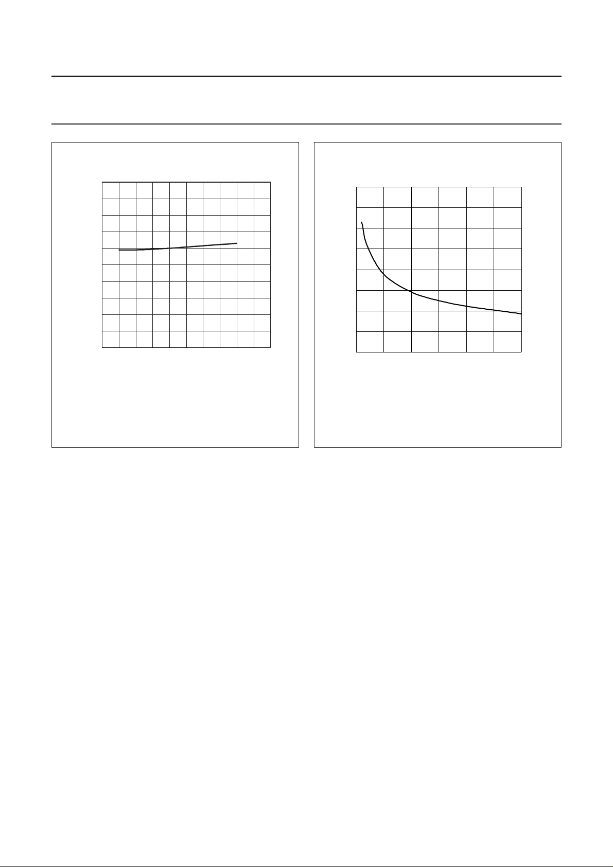
100
h
FE
80
60
40
20
0
0246810
VCE=10V.
I
C
(mA)
Fig.2 DC current gain as a function of collector
current (per section); typical values.
160
handbook, halfpage
C
re
(pF)
120
80
40
0
0102030
f=1MHz.
VCB (V)
Fig.3 Feedback capacitance as a function of
collector-base voltage (per section);
typical values.
MBK397
1999 Apr 23 4
Philips Semiconductors Preliminary specification
UHF push-pull power transistor BLV2048
APPLICATION INFORMATION
RF performance at T
=25°C in a common emitter test circuit; bias circuit: Ri=0.2Ω.
h
MODE OF
OPERATION
f
(MHz)
V
(V)
CE
I
CQ
(mA)
P
(W)
L
G
p
(dB)
η
(%)
C
d
im
(dBc)
ACP
(dBc)
CW, class-AB 2000 26 2x300 120 ≥8 ≥40 −−
2-tone, class-AB f
CDMA, class-AB 2000 26 2x500 25 typ. 9 typ. 22 −
= 2000.0; f2= 2000.1 26 2x300 120 (PEP) ≥8.5 ≥33 ≤−28 −
1
≤−46
(note 1)
Notes
1. CDMA testsignal with peak to average ratio of 11.9dB.
ACP is measured at +/- 885 kHz offset from the centre of the channel (2000 MHz) using a spectrum analyzer with a
resolution set to 30 kHz
Ruggedness in class-AB operation
The BLV2048 is capable of withstanding a load mismatch corresp onding to VSWR = 3 : 1 through all phases under the
following conditions : f
= 2000.0 MHz; f2= 2000.1 MHz; VCE= 26 V; ICQ= 2 x 300 mA; PL= 120 W (PEP); Tmb=25°C.
1
12
G
P
(dB)
10
(1)
(2)
8
6
4
2
0
0 20406080100120140
(1) ICQ= 2x300 mA
(2) I
= 2x100 mA
CQ
(3) I
= 2x50 mA
CQ
V
=26V; R1=R2=0; f=2000MHz
CE
(3)
P
Fig.4 Power gain and collector efficiency as a
function of load power; typical values.
(W)
L
60
η
C
(%)
50
G
P
η
C
40
30
20
10
0
12
G
P
(dB)
10
(1)
(2)
8
(3)
6
4
2
0
0 20406080100120140
(1) ICQ= 2x300 mA
(2) I
= 2x100 mA
CQ
(3) I
= 2x50 mA
CQ
V
=26V; R1=R2=2.4Ω; f = 2000 MHz
CE
G
P
η
C
60
η
C
(%)
(3)
50
(2)
(1)
40
30
20
10
0
(W)
P
L
Fig.5 Power gain and collector efficiency as a
function of load power; typical values.
1999 Apr 23 5
 Loading...