Philips BLV2047 Datasheet

DISCRETE SEMICONDUCTORS
DATA SH EET
M3D372
BLV2047
UHF power transistor
Product specification
Supersedes data of 1999 Jan 28
1999 Jun 09

Philips Semiconductors Product specification
UHF power transistor BLV2047
FEATURES
• Emitter ballasting resistors for optimum
temperature profile
• Gold metallization ensures excellent reliability
• Internal input and output matching for easy design of
wideband circuits
• AlN substrate package for environmental safety.
APPLICATIONS
• Common emitter class-AB operation for PCN
(Personal Communication Networks) and
PCS (Personal Communication Services) base station
applications in the 1800 to 2000 MHz frequency range.
DESCRIPTION
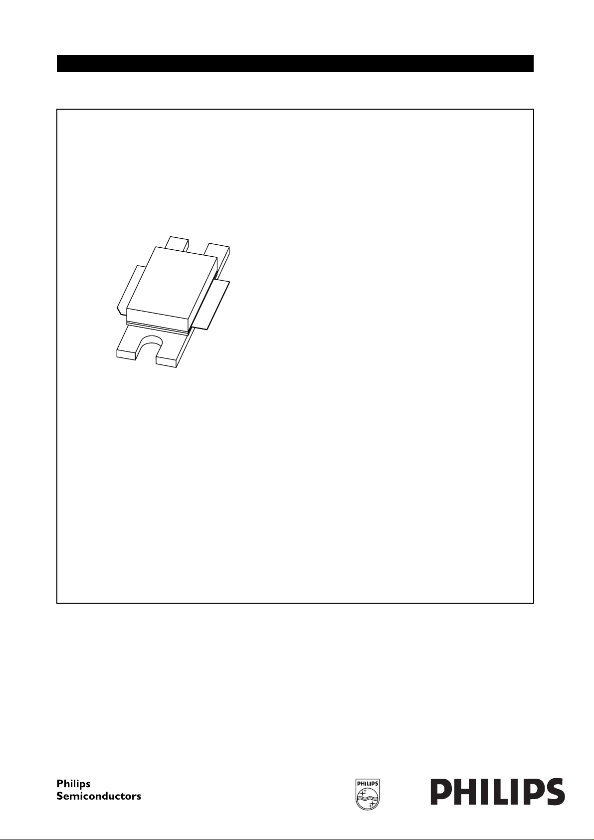
NPN silicon planar power transistor in a 2-lead SOT468A
flange package with ceramic cap. The emitter is connected
to the flange.
QUICK REFERENCE DATA
RF performance at T
=25°C in a common emitter test circuit.
h
PINNING - SOT468A
PIN DESCRIPTION
1 collector
2 base
3 emitter; connected to flange
handbook, halfpage
Top view
Fig.1 Simplified outline.
1
3
2
MBK200
MODE OF OPERATION
f
(MHz)
V
(V)
CE
P
(W)
L
G
p
(dB)
η
(%)
C
d
im
(dBc)
CW, class-AB 2000 26 60 ≥8.5 ≥40 −
2-tone, class-AB f1= 2000.0; f2= 2000.1 26 60 (PEP) ≥9 ≥33 ≤−30
LIMITING VALUES
In accordance with the Absolute Maximum Rating System (IEC 134).
SYMBOL P ARAMETER CONDITIONS MIN. MAX. UNIT
V
CBO
V
CEO
V
EBO
I
C
P
tot
T
stg
T
j
collector-base voltage open emitter − 65 V
collector-emitter voltage open base − 27 V
emitter-base voltage open collector − 3V
collector current (DC) − 10 A
total power dissipation Tmb=25°C − 270 W
storage temperature −65 +150 °C
operating junction temperature − 200 °C
1999 Jun 09 2

Philips Semiconductors Product specification
UHF power transistor BLV2047
THERMAL CHARACTERISTICS
SYMBOL PARAMETER CONDITIONS VALUE UNIT
R
th j-mb
R
th mb-h
thermal resistance from junction to mounting base P
thermal resistance from mounting base to heatsink 0.25 K/W
Note
1. Thermal resistance is determined under specified RF operating conditions.
CHARACTERISTICS
=25°C unless otherwise specified.
T
j
SYMBOL PARAMETER CONDITIONS MIN. TYP. MAX. UNIT
V
(BR)CBO
V
(BR)CEO
V
(BR)EBO
I
CES
h
FE
C
c
collector-base breakdown voltage open emitter; IC=40mA 65 −−V
collector-emitter breakdown voltage open base; IC= 120 mA 27 −−V
emitter-base breakdown voltage open collector; IE=40mA 3 −−V
collector leakage current VCE= 26 V; VBE=0 −−8mA
DC current gain VCE= 10 V; IC=4A 45 − 100
collector capacitance VCB= 26 V; IE=ie= 0; f = 1 MHz;
note 1
C
re
feedback capacitance VCE= 26 V; IC= 0; f = 1 MHz − 41 − pF
= 270 W; Tmb=25°C; note 1 0.65 K/W
tot
− 72 − pF
Note
1. Capacitance of die only.
120
handbook, halfpage
h
FE
80
40
0
0426810
VCE=10V.
MBK396
I
(A)
C
160
handbook, halfpage
C
re
(pF)
120
80
40
0
0102030
f =1 MHz.
MBK397
V
(V)
CB
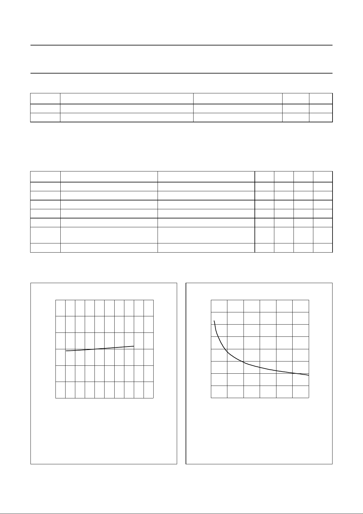
Fig.2 DC current gain as a function of collector
current; typical values.
1999 Jun 09 3
Fig.3 Feedback capacitance as a function of
collector-base voltage; typical values.

Philips Semiconductors Product specification
UHF power transistor BLV2047
APPLICATION INFORMATION
RF performance at T
=25°C in a common emitter test circuit.
h
MODE OF OPERATION
f
(MHz)
V
(V)
CE
I
CQ
(mA)
P
(W)
L
G
p
(dB)
η
(%)
C
d
im
(dBc)
CW, class-AB 2000 26 300 60 ≥8.5 ≥40 −
= 2000.0
f
2-tone, class-AB
1
f2= 2000.1
CDMA, class-AB 2000 26 500 12.5 typ. 9 typ. 22 ≤−46
26 300 60 (PEP) ≥9 ≥33 ≤−30
(1)
Note
1. CDMA test signal with peak to average ratio of 11.9 dB. Adjacent Channel Power (ACP) is measured at ±885 kHz
offset from the centre of the channel (2000 MHz) using a spectrum analyzer with the resolution set to 30 kHz.
Ruggedness in class-AB operation
The BLV2047 is capable of withstanding a load mismatch corresponding to VSWR = 3 : 1 through all phases under the
following conditions: f
12
handbook, halfpage
G
p
(dB)
10
8
6
4
= 2000.0 MHz; f2= 2000.1 MHz; VCE= 26 V; ICQ= 300 mA; PL= 60 W (PEP); Tmb=25°C.
1
MBK398
60
η
C
G
p
η
C
(%)
50
40
30
20
100
handbook, halfpage
P
L
(W)
80
60
40
MBK399
(1)
(2)
(3)
2
0
04020 60 80 100
VCE=26V; ICQ= 300mA; f = 2000 MHz.
PL (W)
10
0
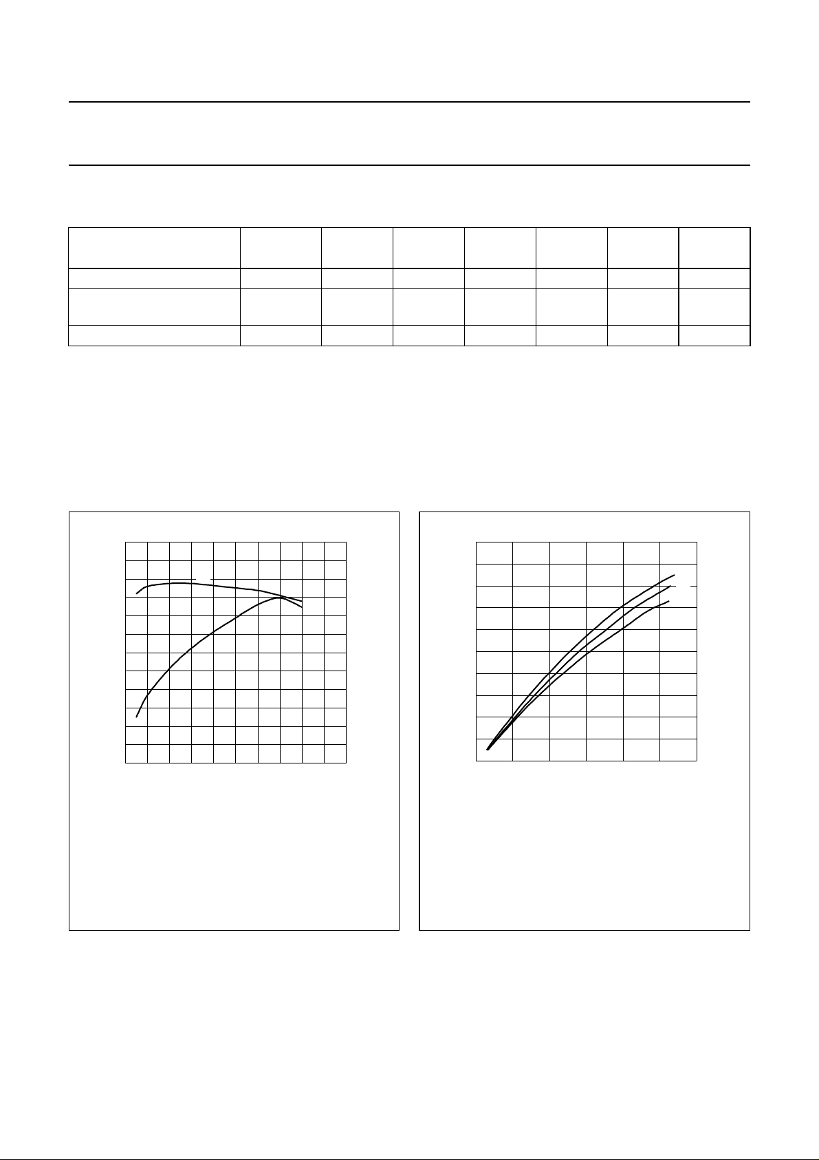
Fig.4 Power gain and collector efficiency as a
function of load power; typical values.
1999 Jun 09 4
20
0
08412
ICQ= 300 mA; f = 2000 MHz.
(1) VCE=28V.
(2) VCE=26V.
(3) VCE=24V.
P
(W)
D
Fig.5 Load power as a function of drive power;
typical values.
 Loading...