

Philips blv2045 DATASHEETS

DISCRETE SEMICONDUCTORS
DATA SH EET
BLV2045
UHF power transistor
Product specification
Supersedes data of 1996 Feb 09
1996 Nov 13
Philips Semiconductors Product specification
UHF power transistor BLV2045
FEATURES
• Emitter ballasting resistors for optimum temperature
profile
• Gold metallization ensures excellent reliability
• Internal input and output matching to achieve high
power gain and collector efficiency for an easy design of
wideband circuits.
APPLICATIONS
• Common emitter class-AB operation in base station
transmitters in the 1800 to 1990 MHz frequency range.
DESCRIPTION
NPN silicon planar transistor in a 2-lead SOT390A flange
package with a ceramic cap. The emitter is connected to
the flange.
QUICK REFERENCE DATA
RF performance at T
=25°C in a common emitter test circuit.
h
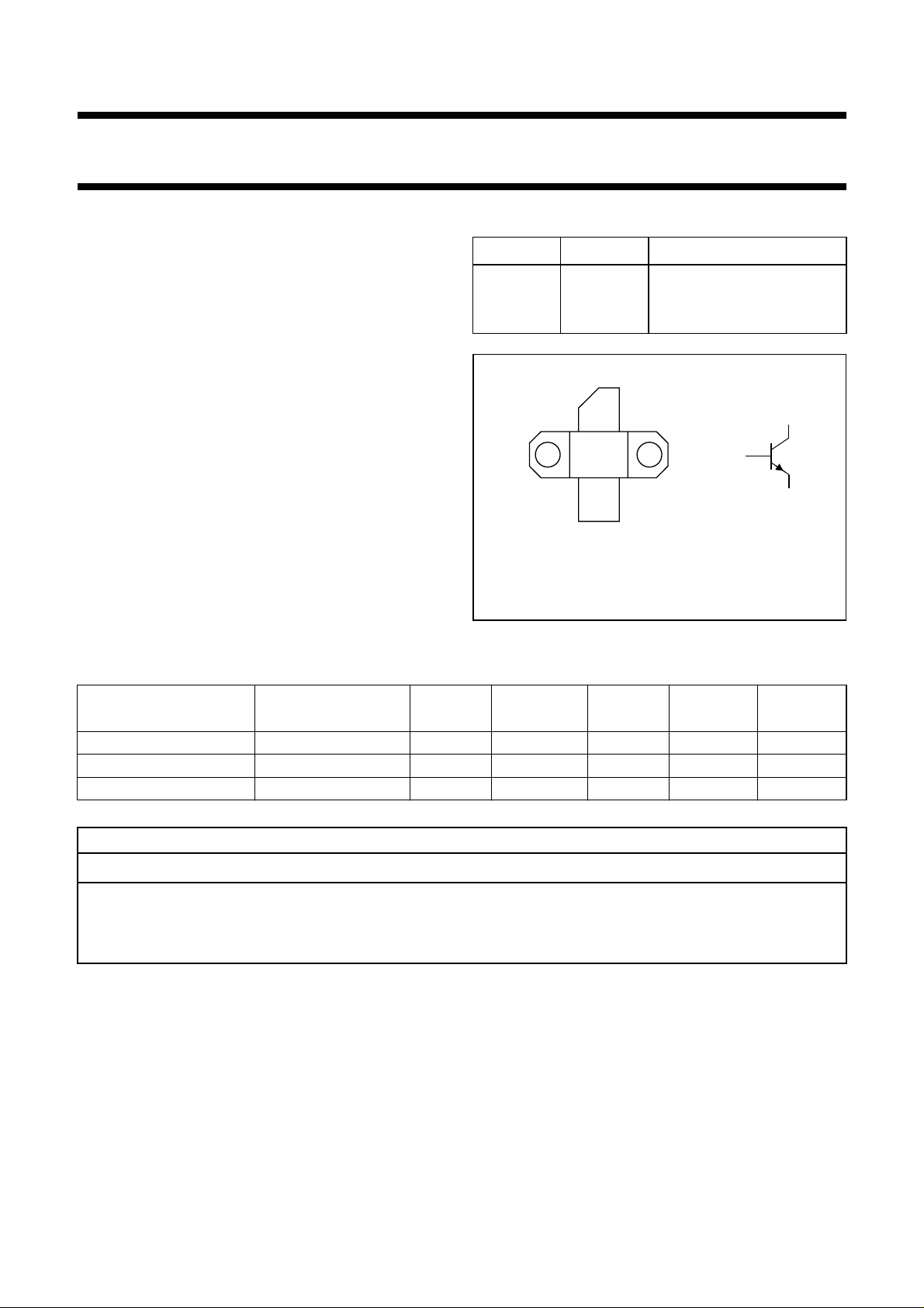
PINNING - SOT390A
PIN SYMBOL DESCRIPTION
1 c collector
2 b base
3 e emitter, connected to flange
handbook, halfpage
1
3
2
MAM228
Top view
b
Fig.1 Simplified outline and symbol.
c
e
MODE OF OPERATION
f
(MHz)
V
(V)
CE
P
(W)
L
G
p
(dB)
η
(%)
C
d
im
(dBc)
CW, class-AB 1950 26 30 ≥8 ≥40 −
CW, class-AB 1990 26 30 ≥8 ≥40 −
2-tone, class-AB f
= 1950; f2= 1950.1 26 30 (PEP) typ. 9 typ. 35 typ. −30
1
WARNING
Product and environmental safety - toxic materials
This product contains beryllium oxide. The product is entirely safe provided that the BeO disc is not damaged.
All persons who handle, use or dispose of this product should be aware of its nature and of the necessary safety
precautions. After use, dispose of as chemical or special waste according to the regulations applying at the location of
the user. It must never be thrown out with the general or domestic waste.
1996 Nov 13 2
Philips Semiconductors Product specification
UHF power transistor BLV2045
LIMITING VALUES
In accordance with the Absolute Maximum Rating System (IEC 134).
SYMBOL PARAMETER CONDITIONS MIN. MAX. UNIT
V
CBO
V
CEO
V
EBO
I
C
I
C(AV)
P
tot
T
stg
T
j
THERMAL CHARACTERISTICS
SYMBOL PARAMETER CONDITIONS VALUE UNIT
R
th j-mb
R
th mb-h
collector-base voltage open emitter − 60 V
collector-emitter voltage open base − 28 V
emitter-base voltage open collector − 2.5 V
collector current (DC) − 7A
average collector current − 7A
total power dissipation Tmb=25°C − 100 W
storage temperature −65 +150 °C
operating junction temperature − 200 °C
thermal resistance from junction to
P
= 100 W; Tmb=25°C 1.75 K/W
tot
mounting base
thermal resistance from mounting base
0.4 K/W
to heatsink
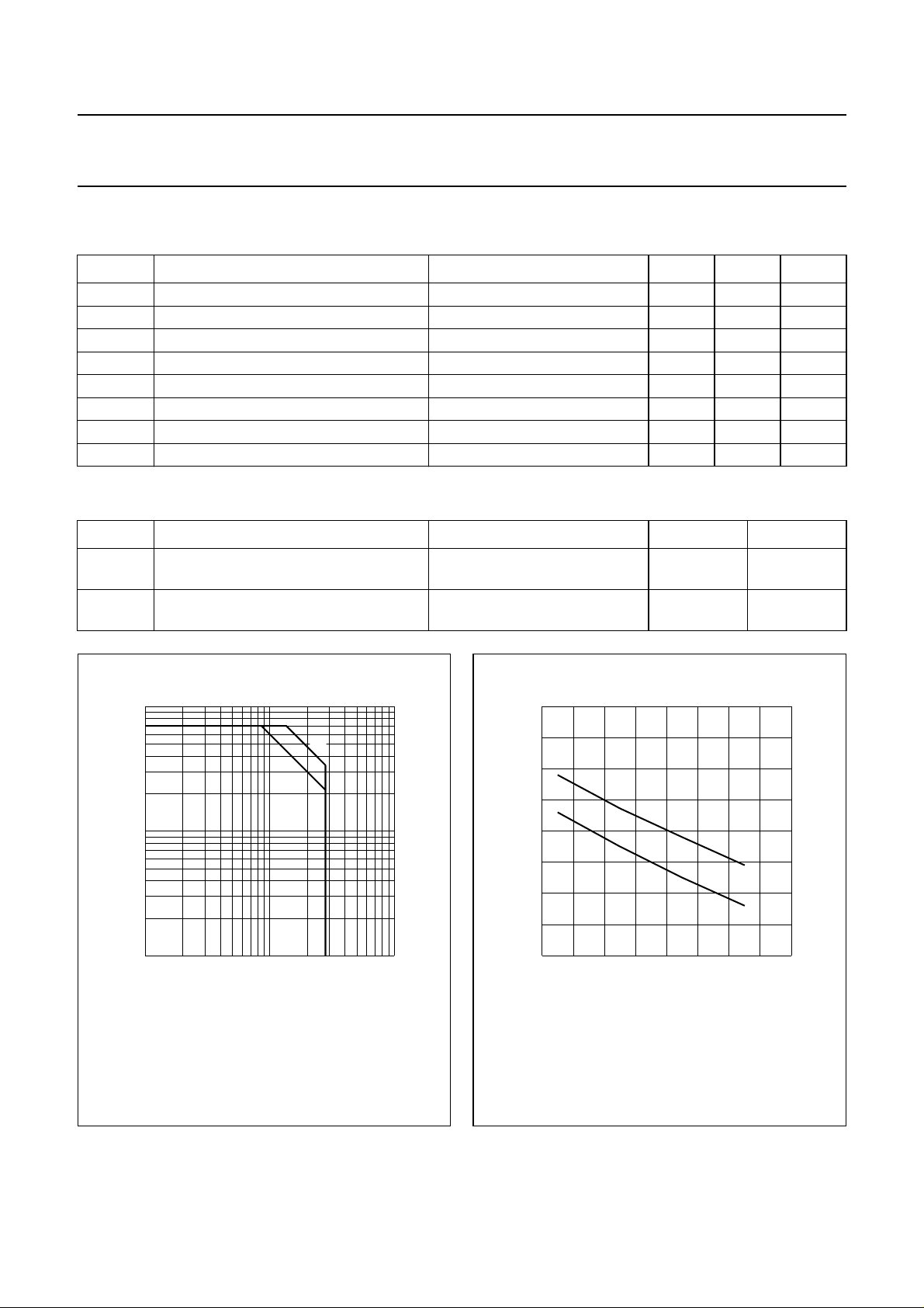
10
handbook, halfpage
I
C
(A)
1
−1
10
11010
(1) Tmb=25°C.
(2) Th=70°C.
(2)
Fig.2 DC SOAR.
(1)
VCE (V)
MGG292
2
160
handbook, halfpage
P
tot
(W)
120
(2)
80
(1)
40
0
0 40 160
(1) Continuous operation.
(2) Short-time operation during mismatch.
80 120
Fig.3 Power derating curves.
MGG293
Th (°C)
1996 Nov 13 3
Philips Semiconductors Product specification
UHF power transistor BLV2045
CHARACTERISTICS
T
=25°C unless otherwise specified.
j
SYMBOL PARAMETER CONDITIONS MIN. TYP. MAX. UNIT
V
(BR)CBO
V
(BR)CEO
V
(BR)EBO
I
CES
h
FE
C
c
C
re
Note
1. Capacitance of die only.
collector-base breakdown voltage open emitter; IC=40mA 60 −−V
collector-emitter breakdown voltage open base; IC=20mA 28 −−V
emitter-base breakdown voltage open collector; IE=1mA 2.5 −−V
collector leakage current VCE= 12.5 V; VBE=0 −−8mA
DC current gain VCE= 24 V; IC= 2 A 45 60 −
collector capacitance VCB= 26 V; IE=ie= 0; f = 1 MHz;
− 32 − pF
note 1
feedback capacitance VCE= 26 V; IC= 0; f = 1 MHz − 20 − pF
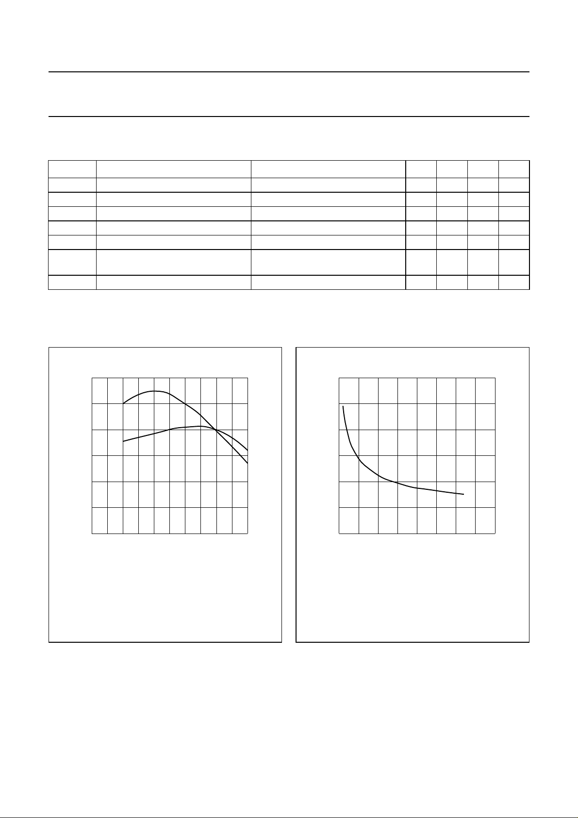
120
h
FE
80
40
0
0
(1) VCE= 26V; tp= 500 µs; δ =<1%.
(2) VCE=10V.
210468
(1)
(2)
MGG294
IC (A)
Fig.4 DC current gain as a function of collector
current; typical values.
60
handbook, halfpage
C
re
(pF)
40
20
0
01020 4030
f = 1 MHz.
VCE (V)
Fig.5 Feedback capacitance as a function of
collector-emitter voltage; typical values.
MGG295
1996 Nov 13 4
Philips Semiconductors Product specification
UHF power transistor BLV2045
APPLICATION INFORMATION
RF performance at T
=25°C in a common emitter test circuit.
h
MODE OF OPERATION
f
(MHz)
CW, class-AB 1950 26 80 30
V
CE
(V)
I
CQ
(mA)
P
(W)
L
G
p
(dB)
≥8 ≥40
typ. 8.5 typ. 45
η
(%)
C
d
im
(dBc)
−
CW, class-AB (note 1) 1990 26 80 30 ≥8 ≥40 −
2-tone, class-AB f1= 1950; f2= 1950.1 26 80 30 (PEP) typ. 9 typ. 35 typ. −30
Note
1. See application note BLV2045.
Ruggedness in class-AB operation
The BLV2045 is capable of withstanding a load mismatch corresponding to VSWR = 5 : 1 through all phases under the
following conditions: f = 1950 MHz; V
12
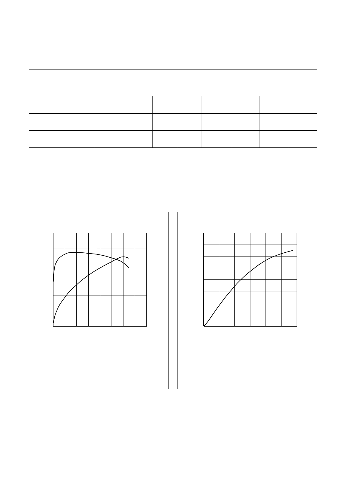
handbook, halfpage
G
p
(dB)
8
G
p
η
C
= 26 V; ICQ= 80 mA; PL=30W;Tmb=25°C.
CE
MGD249
60
η
(%)
40
C
40
handbook, halfpage
P
L
(W)
30
MGD250
4
0
0
VCE= 26 V; ICQ= 80 mA; f = 1950 MHz.
10 20 40
30
PL (W)
Fig.6 Power gain and collector efficiency as
functions of load power; typical values.
20
20
10
0
0
0246
VCE= 26 V; ICQ= 80 mA; f = 1950 MHz.
PD (W)
Fig.7 Load power as a function of drive power;
typical values.
1996 Nov 13 5
 Loading...