

Philips BLV2042 Datasheet

DISCRETE SEMICONDUCTORS
DATA SH EET
BLV2042
UHF power transistor
Product specification
Supersedes data of 1996 Feb 09
1997 Jul 11

Philips Semiconductors Product specification
UHF power transistor BLV2042
FEATURES
• Emitter ballasting resistors for optimum
temperature profile
• Gold metallization ensures excellent reliability
• Internal input matching to achieve high power gain and
easy design of wideband circuits.
APPLICATIONS
• Common emitter class-AB operation in base stations in
the 1800 to 1990 MHz frequency range.
DESCRIPTION
NPN silicon planar epitaxial power transistor in an 8-lead
SOT409B SMD package with ceramic cap.
All leads are isolated from the mounting base.
QUICK REFERENCE DATA
RF performance at T
MODE OF OPERATION
=25°C in a common emitter test circuit.
mb
f
(MHz)
CW, class-AB 1950 26 4 ≥11 ≥40 −
CW, class-AB 1990 26 4 ≥11 ≥40 −
2-tone, class-AB f
= 1950; f2= 1950.1 26 4 (PEP) typ. 14 typ. 35 typ. −30
1
PINNING - SOT409B
PIN DESCRIPTION
1, 4, 5, 8 emitter
2, 3 base
6, 7 collector
handbook, halfpage
85
14
Top view
Fig.1 Simplified outline and symbol.
V
(V)
CE
P
(W)
L
G
(dB)
c
b
MSA467
p
η
C
(%)
e
d
im
(dBc)
1997 Jul 11 2
Philips Semiconductors Product specification
UHF power transistor BLV2042
LIMITING VALUES
In accordance with the Absolute Maximum Rating System (IEC 134).
SYMBOL PARAMETER CONDITIONS MIN. MAX. UNIT
V
CBO
V
CEO
V
EBO
I
C
I
C(AV)
P
tot
T
stg
T
j
Note
1. Transistor with metallized ground plane mounted on a printed-circuit board, see
recommendations in the General part of handbook SC19a”
collector-base voltage open emitter − 60 V
collector-emitter voltage open base − 28 V
emitter-base voltage open collector − 4V
collector current (DC) − 1.2 A
collector current (average) − 1.2 A
total power dissipation Tmb=25°C; note 1 − 17 W
storage temperature −65 +150 °C
operating junction temperature − 200 °C
“Mounting and soldering
.
10
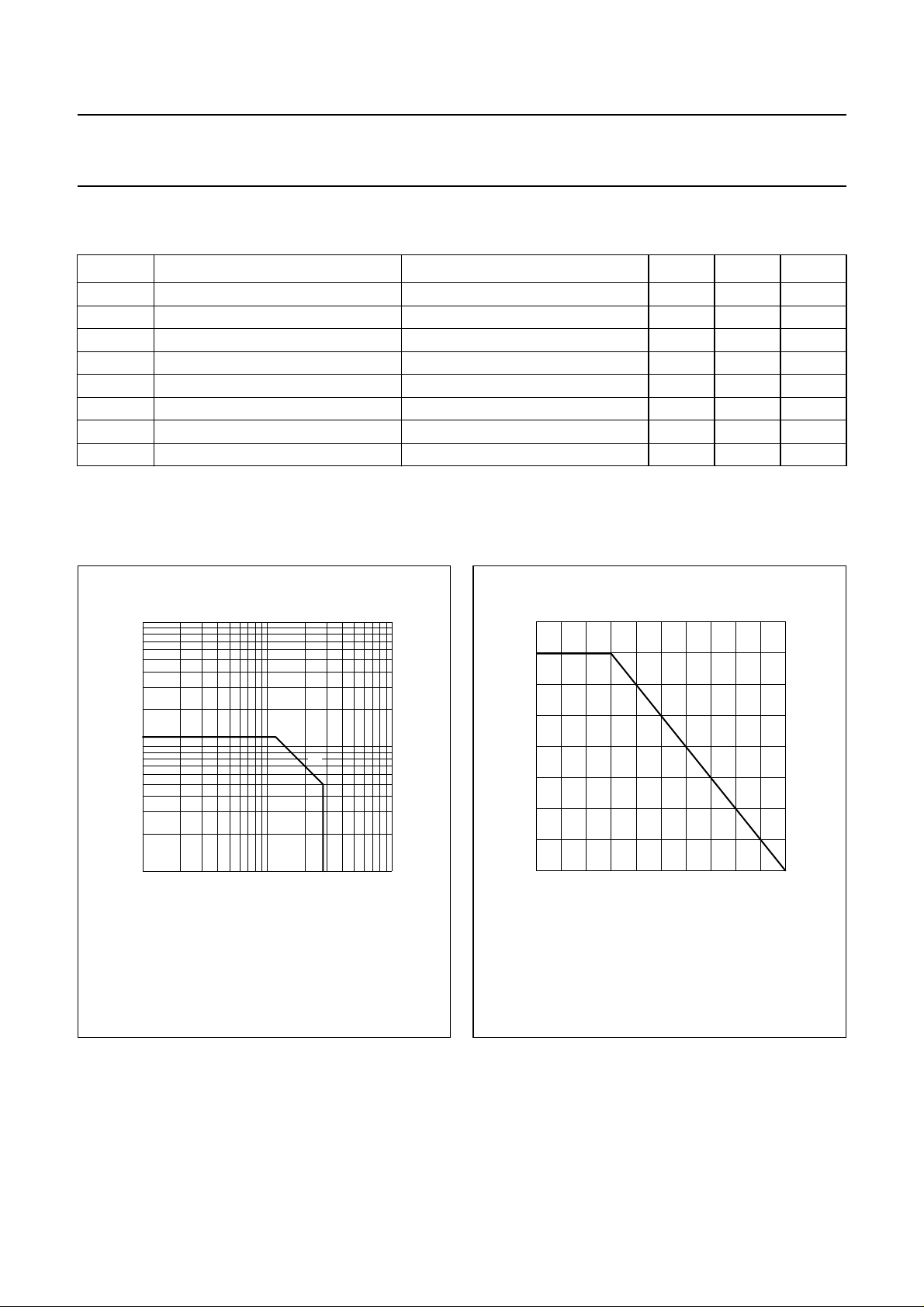
handbook, halfpage
I
C
(A)
1
−1
10
11010
(1) Ts=60°C.
Fig.2 DC SOAR.
MGD934
(1)
V
(V)
CE
2
16
handbook, halfpage
P
tot
(W)
12
8
4
0
0 40 200
80 120 160
MGD935
Ts (°C)
Fig.3 Total power dissipation as a function of the
soldering point temperature.
1997 Jul 11 3
Philips Semiconductors Product specification
UHF power transistor BLV2042
THERMAL CHARACTERISTICS
SYMBOL PARAMETER CONDITIONS VALUE UNIT
R
th j-mb
Note
1. Transistor with metallized ground plane mounted on a printed-circuit board, see
recommendations in the General part of handbook SC19a”
CHARACTERISTICS
T
=25°C unless otherwise specified.
j
SYMBOL PARAMETER CONDITIONS MIN. TYP. MAX. UNIT
V
(BR)CBO
V
(BR)CEO
V
(BR)EBO
I
CES
h
FE
C
c
C
re
thermal resistance from junction to
P
= 17 W; Tmb=25°C; note 1 10 K/W
tot
mounting base
“Mounting and soldering
.
collector-base breakdown voltage open emitter; IC= 5 mA 60 −−V
collector-emitter breakdown voltage open base; IC=10mA 28 −−V
emitter-base breakdown voltage open collector; IE= 0.5 mA 4 −−V
collector leakage current VCE= 26 V; VBE=0 −−1.3 mA
DC current gain VCE= 26 V; IC= 600 mA 30 − 120
collector capacitance VCB= 26 V; IE=ie= 0; f = 1 MHz − 6 − pF
feedback capacitance VCE= 26 V; IC= 0; f = 1 MHz − 2.5 − pF
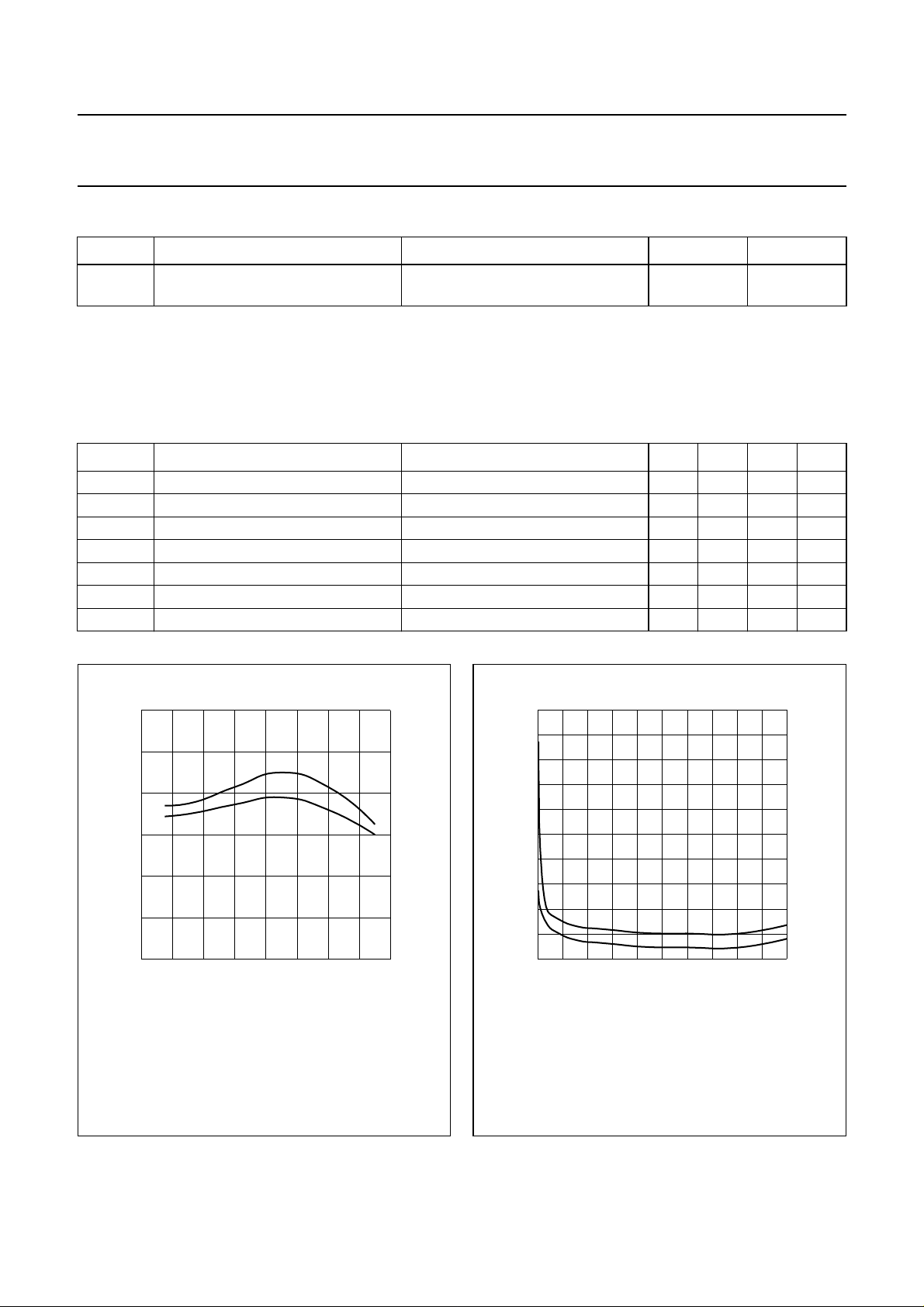
120
handbook, halfpage
h
FE
80
40
0
0
(1) VCE= 26V; tp= 500µs; δ =<1%.
(2) VCE=10V.
0.4 0.8 1.61.2
(1)
(2)
Fig.4 DC current gain as a function of collector
current; typical values.
MGD936
IC (A)
50
handbook, halfpage
C
(pF)
40
30
20
10
f = 1 MHz.
C
c
C
0
re
050
10 20 30 40
Fig.5 Capacitance as a function of
collector-emitter voltage; typical values.
MGD947
VCE (V)
1997 Jul 11 4
Philips Semiconductors Product specification
UHF power transistor BLV2042
APPLICATION INFORMATION
RF performance at T
=25°C in a common emitter test circuit.
mb
MODE OF OPERATION
f
(MHz)
CW, class-AB 1950 26 15 4
V
(V)
CE
I
CQ
(mA)
P
(W)
L
G
p
(dB)
≥11 ≥40
typ. 13 typ. 45
η
(%)
C
d
im
(dBc)
−
CW, class-AB 1990 26 15 4 ≥11 ≥40 −
2-tone, class-AB f1= 1950; f2= 1950.1 26 15 4 (PEP) typ. 14 typ. 35 typ. −30
Ruggedness in class-AB operation
The BLV2042 is capable of withstanding a load mismatch corresponding to VSWR = 20 : 1 through all phases under the
following conditions: f = 1950 MHz; V
16
handbook, halfpage
G
(dB)
12
p
8
G
p
η
C
= 26 V; ICQ= 15 mA; PL= 4 W; Tmb=25°C.
CE
MGD948
80
η
(%)
60
40
handbook, halfpage
C
P
(W)
6
L
4
MGD949
4
0
01 5
CW, class-AB; VCE= 26 V; ICQ= 15 mA; f = 1950 MHz; Tmb=25°C.
23 4
20
0
PL (W)
Fig.6 Power gain and collector efficiency as
functions of load power; typical values.
2
0
0
CW, class-AB; VCE= 26 V; ICQ= 15 mA; f = 1950 MHz; Tmb=25°C.
0.1 0.2 0.3
PD (W)
Fig.7 Load power as a function of drive power;
typical values.
1997 Jul 11 5
 Loading...