

Philips BLT81 Datasheet

DISCRETE SEMICONDUCTORS
DATA SH EET
BLT81
UHF power transistor
Product specification
Supersedes data of November 1992
1996 May 09
Philips Semiconductors Product specification
UHF power transistor BLT81
FEATURES
• SMD encapsulation
• Gold metallization ensures excellent reliability.
APPLICATIONS
• Hand-held radio equipment in the 900 MHz
communication band.
DESCRIPTION
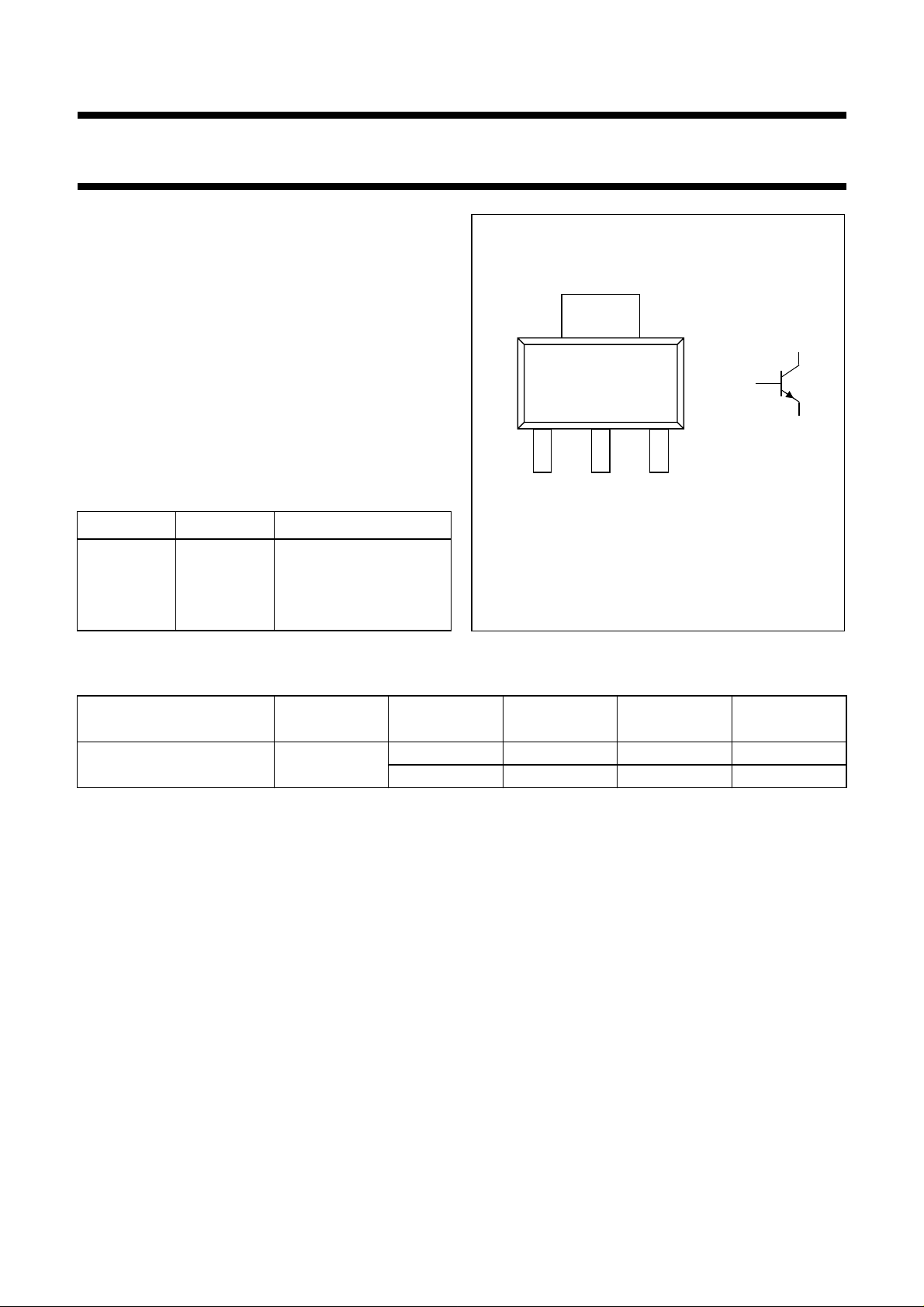
NPN silicon planar epitaxial transistor encapsulated in a
plastic SOT223 SMD package.
PINNING - SOT223
PIN SYMBOL DESCRIPTION
1 e emitter
2 b base
3 e emitter
4 c collector
QUICK REFERENCE DATA
RF performance at T
MODE OF OPERATION
≤ 60 °C in a common emitter test circuit (see Fig.7).
s
f
(MHz)
CW, class-B narrow band 900
handbook, halfpage
123
Top view
4
b
MAM043 - 1
Fig.1 Simplified outline and symbol.
V
(V)
CE
P
(W)
L
G
p
(dB)
η
(%)
7.5 1.2 ≥6 ≥60
6 1.2 typ. 6.5 typ. 77
c
e
C
1996 May 09 2
Philips Semiconductors Product specification
UHF power transistor BLT81
LIMITING VALUES
In accordance with the Absolute Maximum Rating System (IEC 134).
SYMBOL PARAMETER CONDITIONS MIN. MAX. UNIT
V
CBO
V
CEO
V
EBO
I
C
I
C(AV)
P
tot
T
stg
T
j
THERMAL CHARACTERISTICS
SYMBOL PARAMETER CONDITIONS VALUE UNIT
R
th j-s
collector-base voltage open emitter − 20 V
collector-emitter voltage open base − 9.5 V
emitter-base voltage open collector − 2.5 V
collector current (DC) − 500 mA
average collector current − 500 mA
total power dissipation Ts=110°C; note 1 − 2W
storage temperature −65 +150 °C
operating junction temperature − 175 °C
thermal resistance from junction to soldering point P
=2W; Ts=110°C; note 1 32 K/W
tot
Note to the “Limiting values” and “Thermal characteristics”
is the temperature at the soldering point of the collector pin.
1. T
s
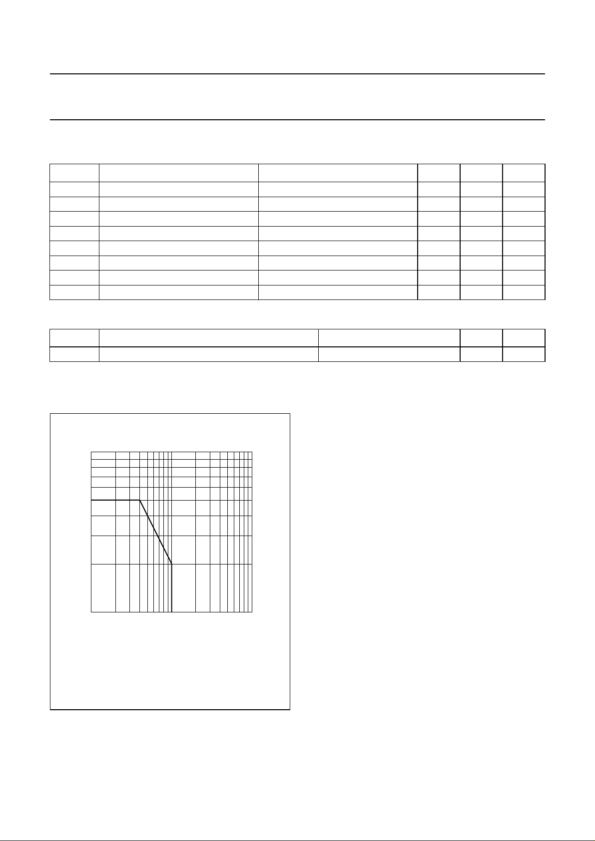
VCE (V)
MRC094
2
10
handbook, halfpage
1
I
C
(A)
−1
10
110
Ts= 110°C.
Fig.2 DC SOAR.
1996 May 09 3

Philips Semiconductors Product specification
UHF power transistor BLT81
CHARACTERISTICS
T
=25°C unless otherwise specified.
j
SYMBOL PARAMETER CONDITIONS MIN. TYP. MAX. UNIT
V
(BR)CBO
V
(BR)CEO
V
(BR)EBO
I
CES
h
FE
C
c
C
re
Note
1. Measured under pulsed conditions: t
collector-base breakdown voltage open emitter; IC= 1 mA 20 −−V
collector-emitter breakdown voltage open base; IC= 10 mA 9.5 −−V
emitter-base breakdown voltage open collector; IE= 0.1 mA 2.5 −−V
collector leakage current VCE= 10 V; VBE=0 −−0.1 mA
DC current gain VCE=5V; IC= 300 mA; note 1; 25 −−
collector capacitance VCB= 7.5 V; IE=ie= 0; f = 1 MHz; − 2.7 4 pF
feedback capacitance VCE= 7.5 V; IC= 0; f = 1 MHz − 1.7 3 pF
≤ 200 µs; δ≤0.02.
p
100
handbook, halfpage
h
FE
80
60
40
20
0
0 100 200 300 400
VCE= 7.5 V; tp≤ 200 µs; δ≤0.02; Tj=25°C.
IC (mA)
Fig.3 DC current gainas a function of collector
current; typical values.
MRC090
handbook, halfpage
6
C
c
(pF)
4
2
0
0246810
IE=ie= 0; f = 1 MHz; Tj=25°C.
Fig.4 Collector capacitance as a function of
collector-base voltage; typical values.
MRC086
VCB (V)
1996 May 09 4
 Loading...