

Philips BLS3135-20 Datasheet
DATA SH EET
Product specification 2000 Feb 01
DISCRETE SEMICONDUCTORS
BLS3135-20
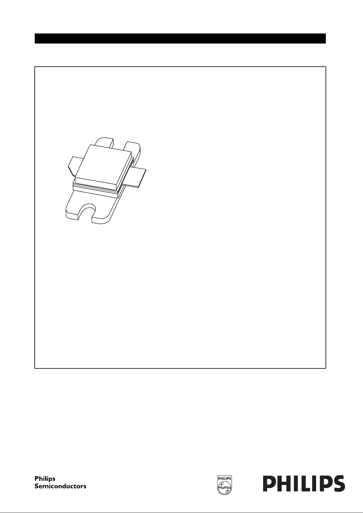
Microwave power transistor
halfpage
M3D259
2000 Feb 01 2
Philips Semiconductors Product specification
Microwave power transistor BLS3135-20
FEATURES
• Suitable for short and medium pulse applications
• Internal inputand output matching networks for an easy
circuit design
• Emitter ballasting resistors improve ruggedness
• Gold metallization ensures excellent reliability
• Interdigitated emitter-base structure provides high
emitter efficiency
• Multicellgeometry improves power sharing andreduces
thermal resistance.
APPLICATIONS
• Commonbaseclass-Cpulsedpoweramplifiersforradar
applications in the 3.1 to 3.5 GHz range.
DESCRIPTION
NPN silicon planar epitaxial microwave powertransistor in
a 2-lead rectangular flange package with a ceramic cap
(SOT422A) with the common base connected to the
flange.
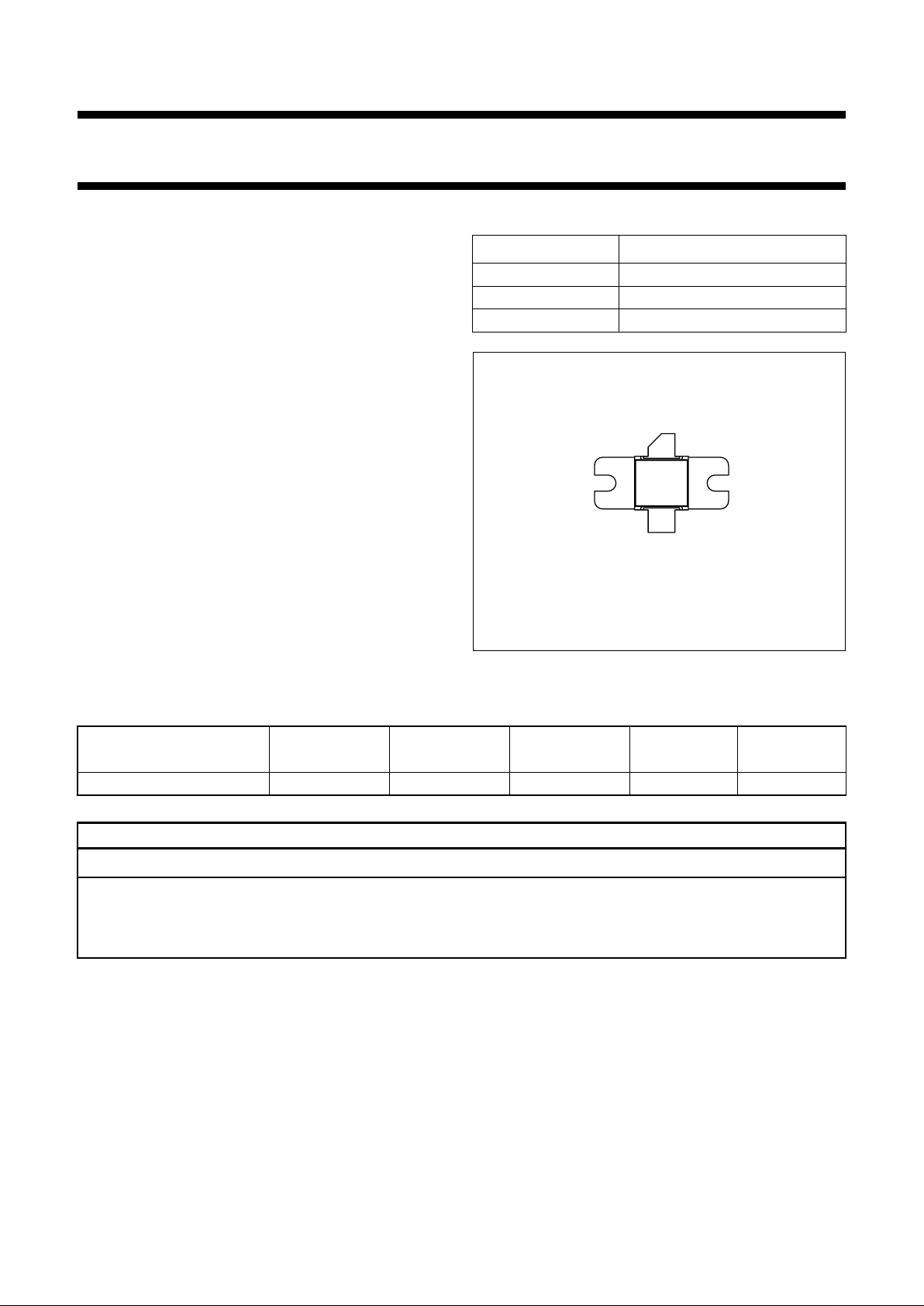
PINNING - SOT422A
PIN DESCRIPTION
1 collector
2 emitter
3 base; connected to flange
handbook, halfpage
1
2
33
MBK051
Fig.1 Simplified outline.
QUICK REFERENCE DATA
RF performance at Th=25°C in a common base class-C test circuit.
MODE OF OPERATION
f
(GHz)
V
CB
(V)
P
L
(W)
G
p
(dB)
η
C
(%)
Pulsed, class-C 3.1 to 3.5 40 20 typ. 8 typ. 40
WARNING
Product and environmental safety - toxic materials
This product contains beryllium oxide. The product is entirely safe provided that the BeO disc is not damaged.
All persons who handle, use or dispose of this product should be aware of its nature and of the necessary safety
precautions. After use, dispose of as chemical or special waste according to the regulations applying at the location of
the user. It must never be thrown out with the general or domestic waste.

2000 Feb 01 3
Philips Semiconductors Product specification
Microwave power transistor BLS3135-20
LIMITING VALUES
In accordance with the Absolute Maximum Rating System (IEC 134).
THERMAL CHARACTERISTICS
Note
1. Equivalent thermal impedance under pulsed microwave operating conditions.
CHARACTERISTICS
Tj=25°C unless otherwise specified.
APPLICATION INFORMATION
RF performance at T
h
=25°C in a common-base test circuit.
SYMBOL PARAMETER CONDITIONS MIN. MAX. UNIT
V
CBO
collector-base voltage open emitter − 75 V
V
CES
collector-emitter voltage RBE=0 − 75 V
V
EBO
emitter-base voltage open collector − 2V
I
CM
peak collector current tp≤ 100 µs; δ≤10% − 2A
P
tot
total power dissipation tp= 100 µs; δ = 10%; Tmb=25°C − 80 W
T
stg
storage temperature −65 +200 °C
T
j
operating junction temperature − 200 °C
T
sld
soldering temperature up to 0.2 mm from ceramic cap;
t ≤ 10 s
− 235 °C
SYMBOL PARAMETER CONDITIONS VALUE UNIT
Z
th j-h
thermal impedance from junction to heatsink tp= 100 µs; δ = 10%; note 1 2 K/W
t
p
= 200 µs; δ = 10%; note 1 2.45 K/W
t
p
= 300 µs; δ = 10%; note 1 2.75 K/W
SYMBOL PARAMETER CONDITIONS MIN. MAX. UNIT
V
(BR)CBO
collector-base breakdown voltage IC= 15 mA; open emitter 75 − V
V
(BR)CES
collector-emitter breakdown voltage IC= 15 mA; VBE=0 75 − V
I
CBO
collector leakage current VCB= 40 V; IE=0 − 0.5 mA
I
CES
collector leakage current VCE= 40 V; VBE=0 − 1mA
I
EBO
emitter leakage current VEB= 1.5 V; IC=0 − 0.1 mA
h
FE
DC current gain VCB=5V; IC= 1.5 A 40 −
MODE OF OPERATION
f
(GHz)
V
CE
(V)
P
L
(W)
G
p
(dB)
η
C
(%)
Class-C; t
p
= 100 µs; δ = 10% 3.1 to 3.5 40 ≥20
typ. 22
≥7
typ. 8
≥35
typ. 40

2000 Feb 01 4
Philips Semiconductors Product specification
Microwave power transistor BLS3135-20
handbook, halfpage
01
(1) (2)
(3)
24
25
0
20
3
PD (W)
P
L
(W)
15
10
5
MCD863
Fig.2 Load power as a function of drive power;
typical values.
VCB= 40 V; class-C; tp= 100 µs; δ = 10%.
(1) f = 3.1 GHz.
(2) f = 3.3 GHz.
(3) f = 3.5 GHz.
handbook, halfpage
025
10
0
2
4
6
8
5101520
P
L
(W)
G
p
(dB)
MCD864
(3)
(1)
(2)
Fig.3 Power gain as a function of load power;
typical values.
VCB= 40 V; class-C; tp= 100 µs; δ = 10%.
(1) f = 3.1 GHz.
(2) f = 3.3 GHz.
(3) f = 3.5 GHz.
handbook, halfpage
025
50
0
10
20
30
40
5101520
P
L
(W)
η
C
(dB)
MCD865
(3)
(1)
(2)
Fig.4 Collector efficiency as a function of load
power; typical values.
VCB= 40 V; class-C; tp= 100 µs; δ = 10%.
(1) f = 3.1 GHz.
(2) f = 3.3 GHz.
(3) f = 3.5 GHz.
handbook, halfpage
3
G
p
(dB)
3.2 3.4
G
p
η
C
3.6
f (GHz)
10
0
8
6
4
2
η
C
(%)
50
0
40
30
20
10
MCD866
Fig.5 Power gain and efficiency as functions of
frequency; typical values.
VCB= 40 V; class-C; PL= 20 W; tp= 100 µs; δ = 10%.
 Loading...