Philips BLF544 Datasheet

DISCRETE SEMICONDUCTORS
DATA SH EET
M3D076
BLF544
UHF power MOS transistor
Product specification
Supersedes data of October 1992
1998 Jan 21

Philips Semiconductors Product specification
UHF power MOS transistor BLF544
FEATURES
• High power gain
• Easy power control
• Good thermal stability
• Gold metallization ensures excellent reliability
• Designed for broadband operation.
APPLICATIONS
• Communication transmitters in the UHF frequency
range.
DESCRIPTION
N-channel enhancement mode vertical D-MOS power
transistor encapsulated in a 6-lead, SOT171A flange
package with a ceramic cap. All leads are isolated from the
flange.
A marking code showing gate-source voltage (V
GS
)
information is provided for matched pair applications.
QUICK REFERENCE DATA
RF performance at T
=25°C in a common source class-B circuit.
h
PINNING - SOT171A
PIN SYMBOL DESCRIPTION
1 s source
2 s source
3 g gate
4 d drain
5 s source
6 s source
handbook, halfpage
Top view
6
g
12345
Fig.1 Simplified outline and symbol.
d
s
MAM390
MODE OF OPERATION
f
(MHz)
V
(V)
DS
P
(W)
L
G
p
(dB)
η
(%)
D
CW, class-B 500 28 20 >11 >50
CW, class-B 960 28 20 typ. 7 typ. 50
CAUTION
This product is supplied in anti-static packing to prevent damage caused by electrostatic discharge during transport
and handling. For further information, refer to Philips specs.: SNW-EQ-608, SNW-FQ-302A and SNW-FQ-302B.
WARNING
Product and environmental safety - toxic materials
This product contains beryllium oxide. The product is entirely safe provided that the BeO disc is not damaged.
All persons who handle, use or dispose of this product should be aware of its nature and of the necessary safety
precautions. After use, dispose of as chemical or special waste according to the regulations applying at the location of
the user. It must never be thrown out with the general or domestic waste.
1998 Jan 21 2

Philips Semiconductors Product specification
UHF power MOS transistor BLF544
LIMITING VALUES
In accordance with the Absolute Maximum System (IEC 134).
SYMBOL PARAMETER CONDITIONS MIN. MAX. UNIT
V
DS
V
GS
I
D
P
tot
T
stg
T
j
THERMAL CHARACTERISTICS
SYMBOL PARAMETER VALUE UNIT
R
th j-mb
R
th mb-h
drain-source voltage − 65 V
gate-source voltage −±20 V
drain current (DC) − 3.5 A
total power dissipation Tmb≤ 25 °C − 48 W
storage temperature −65 150 °C
junction temperature − 200 °C
thermal resistance from junction to mounting base 3.7 K/W
thermal resistance from mounting base to heatsink 0.4 K/W
10
handbook, halfpage
I
D
(A)
(1)
1
−1
10
11010
(1) Current is this area may be limited by R
(2) Tmb=25°C.
Fig.2 DC SOAR.
(2)
VDS (V)
DSon.
MRA992
2
60
handbook, halfpage
P
tot
(W)
40
20
0
0
(1) Short-time operation during mismatch.
(2) Continuous operation.
40 80
(1)
(2)
Fig.3 Power/temperature derating curves.
120
MBK442
Th ( °C)
160
1998 Jan 21 3

Philips Semiconductors Product specification
UHF power MOS transistor BLF544
CHARACTERISTICS
T
=25°C unless otherwise specified.
j
SYMBOL PARAMETER CONDITIONS MIN. TYP. MAX. UNIT
V
(BR)DSS
I
DSS
I
GSS
V
GSth
∆V
GSth
g
fs
R
DSon
I
DSX
C
is
C
os
C
rs
drain-source breakdown voltage VGS= 0; ID=10mA 65 −− V
drain-source leakage current VGS= 0; VDS=28V −−1mA
gate-source leakage current VGS= ±20 V; VDS=0 −−1 µA
gate-source threshold voltage ID= 40 mA; VDS=10V 1 − 4V
gate-source voltage difference of
ID= 40 mA; VDS=10V −−100 mV
matched pairs
forward transconductance ID= 1.2 A; VDS= 10 V 600 900 − mS
drain-source on-state resistance ID= 1.2 A; VGS=10V − 0.85 1.25 Ω
on-state drain current VGS= 15 V; VDS=10V − 4.8 − A
input capacitance VGS= 0; VDS= 28 V; f = 1 MHz − 32 − pF
output capacitance VGS= 0; VDS= 28 V; f = 1 MHz − 24 − pF
feedback capacitance VGS= 0; VDS= 28 V; f = 1 MHz − 6.4 − pF
handbook, halfpage
4
T.C
(mV/K)
2
0
−2
−4
−2
10
VDS=10V.
−1
10
110
ID (A)
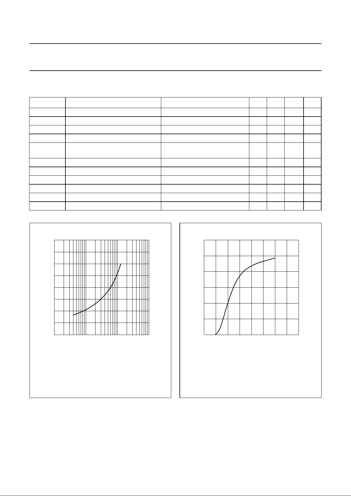
Fig.4 Temperature coefficient of gate-source
voltage as a function of drain current; typical
values.
MDA504
handbook, halfpage
6
I
D
(A)
4
2
0
0
VDS=10V;Tj=25°C.
5
10 20
MDA505
15
V
(V)
GS
Fig.5 Drain current as a function of gate-source
voltage; typical values.
1998 Jan 21 4

Philips Semiconductors Product specification
UHF power MOS transistor BLF544
handbook, halfpage
2
R
DSon
(Ω)
1.6
1.2
0.8
0.4
0
050
ID= 1.2A; VGS=10V.
100 150
Tj (°C)
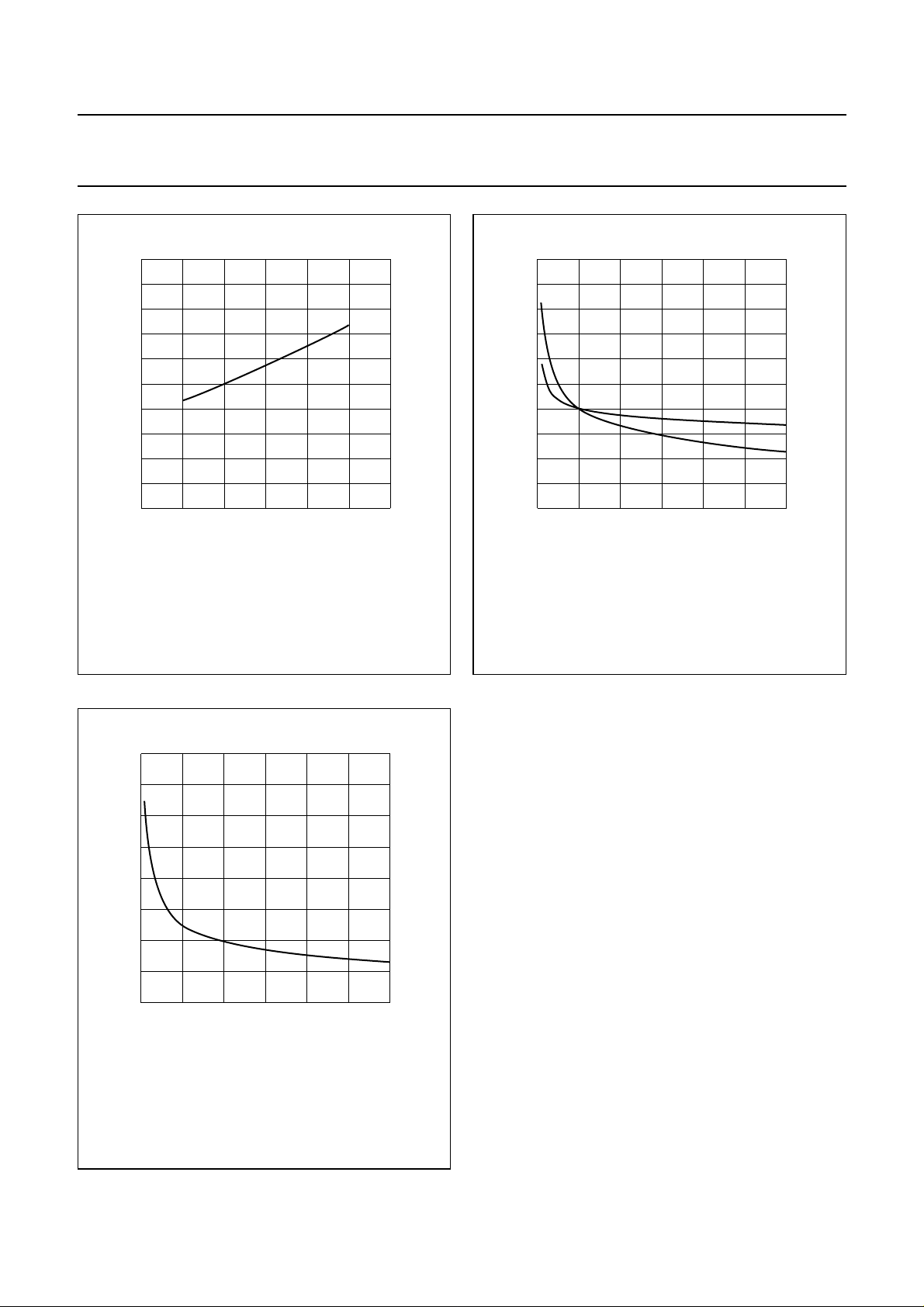
Fig.6 Drain-source on-state resistance as a
function of junction temperature; typical
values.
MDA506
100
handbook, halfpage
C
(pF)
80
60
40
20
0
010
VGS= 0; f= 1 MHz.
20 30
MDA507
C
C
V
(V)
DS
Fig.7 Input and output capacitance as functions
of drain-source voltage; typical values.
is
os
40
handbook, halfpage
C
rs
(pF)
30
20
10
0
0102030
VGS= 0; f = 1 MHz.
VDS (V)
Fig.8 Feedback capacitance as a function of
drain-source voltage; typical values.
MDA508
1998 Jan 21 5
 Loading...