

Philips BLF378 Datasheet

DISCRETE SEMICONDUCTORS
DATA SH EET
M3D091
BLF378
VHF push-pull power MOS
transistor
Product specification
Supersedes data of 1996 Oct 17
1998 Jul 29
Philips Semiconductors Product specification
VHF push-pull power MOS transistor BLF378
FEATURES
• High power gain
• Easy power control
• Good thermal stability
• Gold metallization ensures excellent reliability.
APPLICATIONS
• Broadcast transmitter applications in the VHF frequency
range.
DESCRIPTION
Dual push-pull silicon N-channel enhancement mode
vertical D-MOS transistor encapsulated in a 4-lead,
SOT262A1 balanced flange package with two ceramic
caps. The mounting flange provides the common source
connection for the transistors.
CAUTION
This product is supplied in anti-static packing to prevent
damage caused by electrostatic discharge during
transport and handling. For further information, refer to
Philips specs.: SNW-EQ-608, SNW-FQ-302A, and
SNW-FQ-302B.
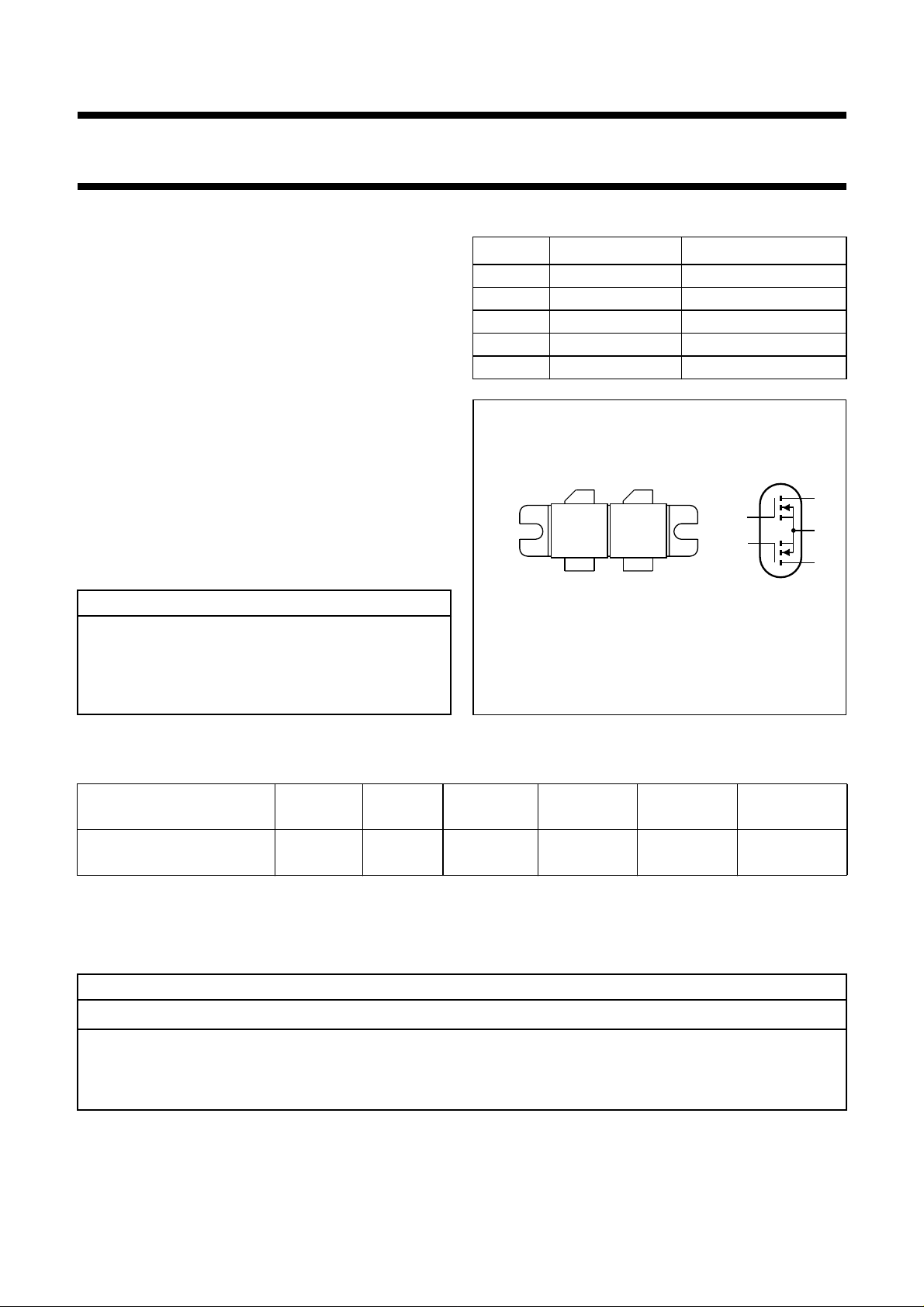
PINNING - SOT262A1
PIN SYMBOL DESCRIPTION
1d
2d
3g
4g
1
2
1
2
drain 1
drain 2
gate 1
gate 2
5 s source
12
g
g
55
Top view
34
MAM098
Fig.1 Simplified outline and symbol.
d
s
d
QUICK REFERENCE DATA
RF performance at T
MODE OF OPERATION
CW, class-AB
=25°C in a push-pull common source test circuit.
h
f
(MHz)
V
(V)
DS
P
(W)
L
225 50 250
G
(dB)
p
∆G
(dB)
p
(1)
η
(%)
D
>14 <1 >50
typ. 16 typ. 0.6 typ. 55
Note
1. Assuming a 3rd order amplitude transfer characteristic, 1 dB gain compression corresponds with 30% synchronized
input / 25% synchronized output compression in television service (negative modulation, CCIR system).
WARNING
Product and environmental safety - toxic materials
This product contains beryllium oxide. The product is entirely safe provided that the BeO discs are not damaged.
All persons who handle, use or dispose of this product should be aware of its nature and of the necessary safety
precautions. After use, dispose of as chemical or special waste according to the regulations applying at the location of
the user. It must never be thrown out with the general or domestic waste.
1998 Jul 29 2
Philips Semiconductors Product specification
VHF push-pull power MOS transistor BLF378
LIMITING VALUES
In accordance with the Absolute Maximum Rating System (IEC 134).
SYMBOL PARAMETER CONDITIONS MIN. MAX. UNIT
Per transistor section unless otherwise specified
V
DSS
V
GSS
I
D
P
tot
T
stg
T
j
THERMAL CHARACTERISTICS
SYMBOL PARAMETER CONDITIONS VALUE UNIT
R
th j-mb
R
th mb-h
drain-source voltage − 110 V
gate-source voltage −±20 V
drain current (DC) − 18 A
total power dissipation Tmb≤ 25 °C total device; both sections equally loaded − 500 W
storage temperature −65 150 °C
junction temperature − 200 °C
thermal resistance from junction to mounting base total device; both sections
0.35 K/W
equally loaded
thermal resistance from mounting base to heatsink total device; both sections
0.15 K/W
equally loaded
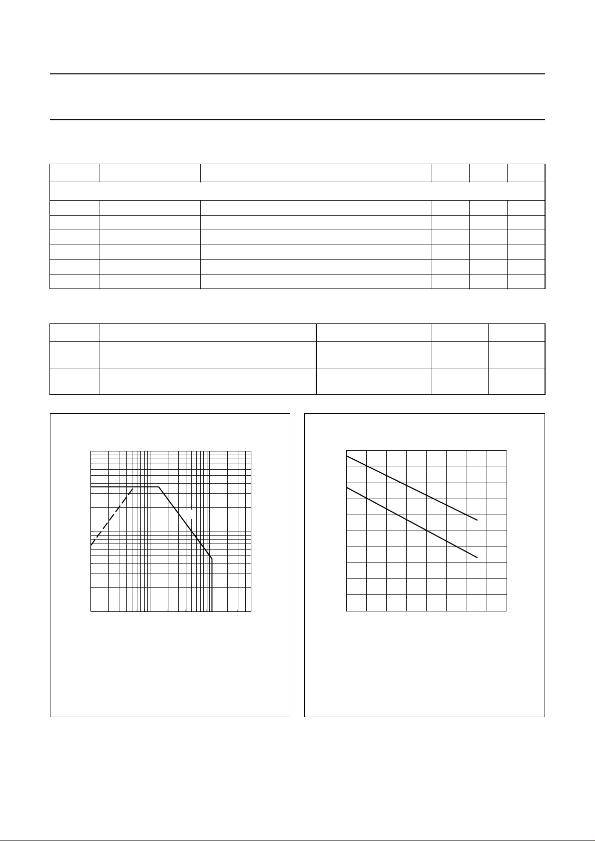
100
handbook, halfpage
I
D
(A)
(1)
10
1
1 10 100
Total device; both sections equally loaded.
(1) Current is this area may be limited by R
(2) Tmb=25°C.
Fig.2 DC SOAR.
(2)
DSon
MRA988
V (V)
DS
.
500
500
handbook, halfpage
P
tot
(W)
400
300
200
100
0
0 40 80 160
Total device; both sections equally loaded.
(1) Continuous operation.
(2) Short-time operation during mismatch.
(1)
Fig.3 Power derating curves.
(2)
120
MGE616
Th (°C)
1998 Jul 29 3
Philips Semiconductors Product specification
VHF push-pull power MOS transistor BLF378
CHARACTERISTICS
T
=25°C unless otherwise specified.
j
SYMBOL PARAMETER CONDITIONS MIN. TYP. MAX. UNIT
Per transistor section
V
(BR)DSS
I
DSS
I
GSS
V
GSth
∆V
GS
g
fs
g
fs1/gfs2
R
DSon
I
DSX
C
is
C
os
C
rs
C
d-f
drain-source breakdown voltage VGS= 0; ID=50mA 110 −−V
drain-source leakage current VGS= 0; VDS=50V −−2.5 mA
gate-source leakage current VGS= ±20 V; VDS=0 −−1µA
gate-source threshold voltage ID= 50 mA; VDS=10V 2.0 − 4.5 V
gate-source voltage difference
ID= 50 mA; VDS=10V −−100 mV
of both transistor sections
forward transconductance ID= 5 A; VDS= 10 V 4.5 6.2 − S
forward transconductance ratio
ID= 5 A; VDS= 10 V 0.9 − 1.1
of both transistor sections
drain-source on-state resistance ID= 5 A; VGS=10V − 0.2 0.3 Ω
on-state drain current VGS= 10 V; VDS=10V − 25 − A
input capacitance VGS= 0; VDS= 50 V; f = 1 MHz − 480 − pF
output capacitance VGS= 0; VDS= 50 V; f = 1 MHz − 190 − pF
feedback capacitance VGS= 0; VDS= 50 V; f = 1 MHz − 14 − pF
drain-flange capacitance − 5.4 − pF
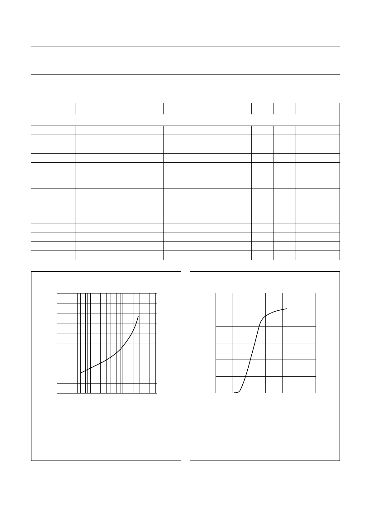
handbook, halfpage
0
T.C.
(mV/K)
−1
−2
−3
−4
−5
10
VDS=10V.
−2
−1
10
110
ID (A)
Fig.4 Temperature coefficient of gate-source
voltage as a function of drain current; typical
values per section.
MGE623
30
handbook, halfpage
I
D
(A)
20
10
0
0
VDS= 10V; Tj=25°C.
5
10
MGE622
VGS (V)
Fig.5 Drain current as a function of gate-source
voltage; typical values per section.
15
1998 Jul 29 4

Philips Semiconductors Product specification
VHF push-pull power MOS transistor BLF378
400
handbook, halfpage
R
DSon
(mΩ)
300
200
100
0
0 50 100 150
ID= 5A; VGS=10V.
Tj (°C)
Fig.6 Drain-source on-state resistance as a
function of junction temperature; typical
values per section.
MGE621
C
is
C
os
VDS (V)
MGE615
1200
handbook, halfpage
C
(pF)
800
400
0
0
VGS= 0; f= 1 MHz.
20
40
Fig.7 Input and output capacitance as functions
of drain-source voltage; typical values per
section.
60
400
handbook, halfpage
C
rs
(pF)
300
200
100
0
010 50
VGS= 0; f = 1 MHz.
20 30 40
VDS (V)
Fig.8 Feedback capacitance as a function of
drain-source voltage; typical values per
section.
MGE620
1998 Jul 29 5
 Loading...