

查询BLF0810-180供应商
DISCRETE SEMICONDUCTORS
DATA SH EET
M3D379
M3D461
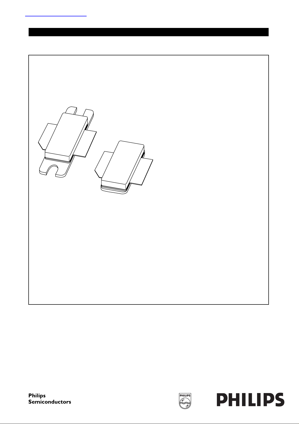
BLF0810-180; BLF0810S-180
Base station LDMOS transistors
Product specification
Supersedes data of 2003 May 09
2003 Jun 12

Philips Semiconductors Product specification
Base station LDMOS transistors BLF0810-180; BLF0810S-180
FEATURES
• Typical CDMA IS95 performance at standard settings
with a supply voltage of 27 V and IDQ of 1130 mA.
Adjacent channel bandwidth is 30 kHz, adjacent
APPLICATIONS
• Common source class-AB operation applications in the
860 to 960 MHz frequency range
• CDMA and multicarrier applications.
channel at ± 750 kHz:
– Output power = 30 W
DESCRIPTION
– Gain = 16 dB
– Efficiency = 27%
180 W LDMOS power transistor for base station
applications at frequencies from 800 to 1000 MHz.
– ACPR = −46 dBc at 750 kHz and BW = 30 kHz
• Easy power control
• Excellent ruggedness
• High power gain
• Excellent thermal stability
• Designed for broadband operation (800 to 1000 MHz)
• Internally matched for ease of use.
PINNING - SOT502A PINNING - SOT502B
PIN DESCRIPTION
1 drain
2 gate
3 source; connected to flange
PIN DESCRIPTION
1 drain
2 gate
3 source; connected to flange
handbook, halfpage
Top view
Fig.1 Simplified outline SOT502A (BLF0810-180).
1
2
3
MBK394
Top view
1
3
2
MBL105
Fig.2 Simplified outline SOT502B (BLF0810S-180).
QUICK REFERENCE DATA
Typical RF performance at Th=25°C in a common source test circuit.
MODE OF OPERATION
Class-AB (2-tone) f
f
(MHz)
= 890.0; f2= 890.1 27 140 (PEP) 16 39 −28 −
1
V
(V)
DS
P
(W)
L
G
(dB)
p
η
D
(%)
d
3
(dBc)
ACPR 750
(dBc)
CDMA (IS95) 890 27 30 (AV) 16 27 −−46
2003 Jun 12 2

Philips Semiconductors Product specification
Base station LDMOS transistors BLF0810-180; BLF0810S-180
LIMITING VALUES
In accordance with the Absolute Maximum Rating System (IEC 60134).
SYMBOL PARAMETER MIN. MAX. UNIT
V
DS
V
GS
T
stg
T
j
THERMAL CHARACTERISTICS
SYMBOL PARAMETER CONDITIONS VALUE UNIT
R
th j-c
R
th j-hs
Notes
1. Thermal resistance is determined under RF operating conditions.
2. Depending on mounting condition in application.
drain-source voltage − 75 V
gate-source voltage −±15 V
storage temperature −65 +150 C
junction temperature − 200 °C
thermal resistance from junction to case Th=25°C, PL= 35 W (AV), note 1 0.42 K/W
thermal resistance from heatsink to junction Th=25°C, PL= 35 W (AV), note 2 0.62 K/W
CHARACTERISTICS
T
=25°C unless otherwise specified.
j
SYMBOL PARAMETER CONDITIONS MIN. TYP. MAX. UNIT
V
(BR)DSS
V
GSth
I
DSS
I
DSX
I
GSS
g
fs
R
DSon
drain-source breakdown voltage VGS= 0; ID= 3 mA 75 −−V
gate-source threshold voltage VDS= 10 V; ID= 300 mA 4 − 5V
drain-source leakage current VGS= 0; VDS=36V −−3µA
on-state drain current VGS=V
+9V; VDS=10V 45 −−A
GSth
gate leakage current VGS= ±20 V; VDS=0 −−1µA
forward transconductance VDS= 10 V; ID=10A − 9 − S
drain-source on-state resistance VGS=9V; ID=10A − 60 − mΩ
2003 Jun 12 3

Philips Semiconductors Product specification
Base station LDMOS transistors BLF0810-180; BLF0810S-180
APPLICATION INFORMATION
RF performance in a common source class-AB circuit.
=27V; IDQ= 1130 mA; f = 890 MHz; Th=25°C; unless otherwise specified.
V
DS
SYMBOL PARAMETER CONDITIONS MIN. TYP. MAX. UNIT
Mode of operation: 2-tone CW, 100 kHz spacing
G
p
η
D
IRL input return loss −−13 −6dB
d
3
G
p
η
D
d
3
Mode of operation: CDMA, IS95 (pilot, paging, sync and traffic codes 8 to 13)
G
p
η
D
ACPR 750 adjacent channel power ratio at BW = 30 kHz −−46 − dBc
gain power PL= 90 W (PEP) 15 16 − dB
drain efficiency 24 30 − %
third order intermodulation
−−40 − dBc
distortion
gain power PL= 125 W (PEP) − 16 − dB
drain efficiency 33 37 − %
third order intermodulation
−−32 −27 dBc
distortion
ruggedness VSWR = 15 : 1 through all
phases; P
= 125 W (PEP)
L
no degradation in output power
gain power PL=30W(AV) − 16 − dB
drain efficiency PL=30W(AV) − 27 − %
2003 Jun 12 4
Philips Semiconductors Product specification
Base station LDMOS transistors BLF0810-180; BLF0810S-180
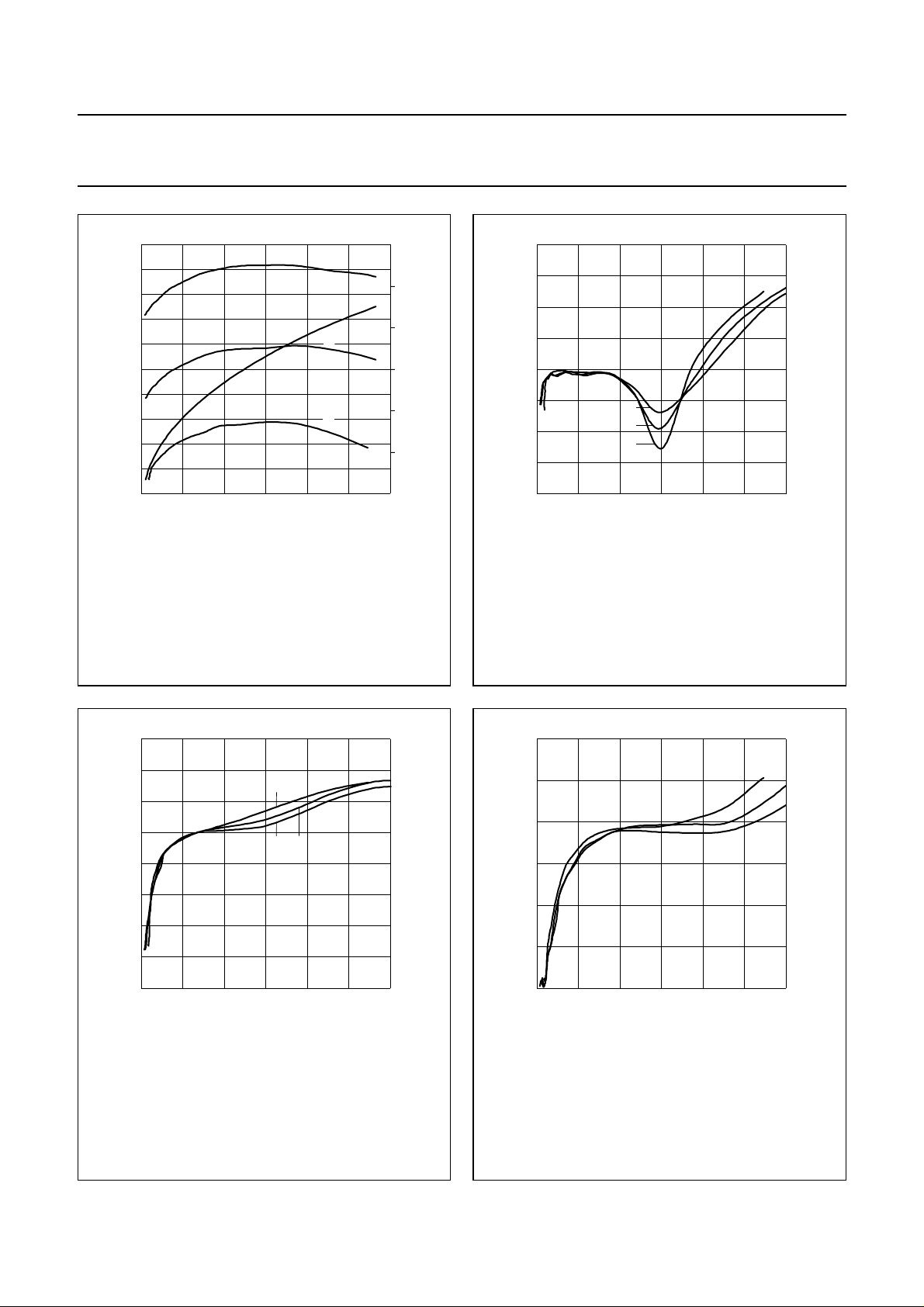
50
handbook, halfpage
η
(%)
40
(4)
η(1,2,3)
30
20
10
0
0 50 100 150
VDS= 27V; IDQ= 1.1 A; f1= 890.0 MHz; f2= 890.1 MHz.
(1) η at T
(2) η at Th=20°C.
(3) η at Th=80°C.
= −40 °C.
h
(4) gain at T
(5) gain at Th=20°C.
(6) gain at Th=80°C.
(5)
(6)
PL (PEP) (W)
Fig.3 2-tone power gain and efficiency as
functions of load power at different
temperatures.
MDB158
= −40 °C.
h
17
16.5
16
15.5
15
14.5
14
gain
(dB)
−20
handbook, halfpage
d
3
(dBc)
−30
−40
(1)
−50
−60
0 50 100 150
VDS= 27 V; IDQ= 1.1 A; f1= 890.0 MHz; f2= 890.1 MHz.
(1) Th= −40 °C.
(2) Th=20°C.
(3) Th=80°C.
(2)
(3)
MDB159
PL (PEP) (W)
Fig.4 Third order intermodulation distortion as a
function of load power at different
temperatures.
−30
handbook, halfpage
d
5
(dBc)
−40
−50
−60
−70
0 50 100 150
VDS= 27 V; IDQ= 1.1 A; f1= 890.0 MHz; f2= 890.1 MHz.
(1) Th= −40 °C.
(2) Th=20°C.
(3) Th=80°C.
(3)
(1)
(2)
MDB160
PL (PEP) (W)
Fig.5 Fifth order intermodulation distortion as a
function of load power at different
temperatures.
−40
handbook, halfpage
d
7
(dBc)
−50
−60
−70
0
VDS= 27 V; IDQ= 1.1 A; f1= 890.0 MHz; f2= 890.1 MHz.
(1) Th= −40 °C.
(2) Th=20°C.
(3) Th=80°C.
50 100 150
MDB161
(3)
(2)
(1)
PL (PEP) (W)
Fig.6 Seventh orderintermodulation distortion as
a function of load power at different
temperatures.
2003 Jun 12 5

Philips Semiconductors Product specification
Base station LDMOS transistors BLF0810-180; BLF0810S-180
20
handbook, halfpage
MDB162
gain
(dB)
15
10
(2)
(1)
(3)
(4)
5
0
0 50 100 150
PL (PEP) (W)
VDS= 27 V; f1= 890.0 MHz; f2= 890.1 MHz.
=1A.
=1A.
(1) I
DQ
(2) IDQ= 1.45 A.
(3) I
DQ
(4) IDQ= 1.45 A.
Fig.7 Powergain and drainefficiency asfunctions
of peakenvelope load power;typical values.
40
30
20
10
0
η
(%)
MDB163
d
im
(dBc)
0
handbook, halfpage
D
−20
(1)
−40
(4)
−60
−80
0 50 100 150
(2)
(5)
(6)
(3)
PL (PEP) (W)
VDS= 27 V; f1= 890.0 MHz; f2= 890.1 MHz.
(1) d3; IDQ=1A.
(2) d5; IDQ=1A.
(3) d7; IDQ=1A.
(4) d3; IDQ= 1.3 A.
(5) d5; IDQ= 1.3 A.
(6) d7; IDQ= 1.3 A.
Fig.8 Intermodulation distortion as a function of
peak envelope load power; typical values.
−45
handbook, halfpage
ACPR
(dBc)
−50
−55
ACPR at 750 kHz
(2)
(1)
MDB164
−60
−65
−70
−75
40
ACPR at 1.98 MHz
(4)
(3)
41 4542 43 44
PL (AV) (dBm)
VDS= 27 V; f = 894 MHz.
= 1.1 A.
(1) IDQ= 1 .1A.
(2) IDQ= 1.4 A.
(3) I
DQ
(4) IDQ= 1.4 A.
Fig.9 CDMA IS95 ACPR distortion as a function
of average load power and IDQ.
−40
handbook, halfpage
MDB165
ACPR
(dBc)
−50
ACPR at 750 kHz
−60
−70
−80
(1)
(2)
ACPR at 1.98 MHz
(3)
(4)
01020 40
30
PL (PEP) (W)
VDS= 27 V; f = 894 MHz; IDQ= 1.1 A.
=20°C.
(1) Th=20°C.
(2) Th=80°C.
(3) T
h
(4) Th=80°C.
Fig.10 CDMA IS95 ACPR distortion as a function
of peak envelope load power at different
temperatures.
2003 Jun 12 6

Philips Semiconductors Product specification
Base station LDMOS transistors BLF0810-180; BLF0810S-180
r
i
x
i
f (GHz)
MDB166
handbook, halfpage
2
Z
i
(Ω)
1.5
1
0.5
0
−0.5
−1
0.85
Class-AB operation; VDS= 27 V; IDQ= 1125 mA; PL=35W.
Values comprised for different parameters.
0.9 0.95 1
Fig.11 Input impedance as afunction of frequency
(series components); typical values.
R
L
X
L
f (GHz)
MDB167
handbook, halfpage
2
Z
L
(Ω)
1.5
1
0.5
0
−0.5
−1
0.85
Class-AB operation; VDS= 27 V; IDQ= 1125 mA; PL=35W.
Values comprised for different parameters.
0.9 0.95 1
Fig.12 Load impedance as afunction of frequency
(series components); typical values.
handbook, halfpage
gate
Z
IN
drain
Z
MGS998
L
Fig.13 Definition of transistor impedance.
2003 Jun 12 7

Philips Semiconductors Product specification
Base station LDMOS transistors BLF0810-180; BLF0810S-180
handbook, full pagewidth
L14
C13
C15
L15 L16
Vsupply
RF out
C18
Vbias
RF in
C2
Q1
R1
C1
L1 L2
C3
C4
L3
L5
L4 L6
C5
C6
L12
L9
C7
L7
L8
C8
Q2
L10
L13
C17
C9
C10
L11
C11
C12
C16
Fig.14 Test circuit for 860 to 900 MHz.
C14
MDB168
2003 Jun 12 8

Philips Semiconductors Product specification
Base station LDMOS transistors BLF0810-180; BLF0810S-180
handbook, full pagewidth
BLF0810-180 output Rev C
C9
C10
C11
C12
C15
C13
C14
C17
C17
C18
C16
C16
C2
C3
C1
R1
C4
C5
C6C6
L5
C7
C8
BLF0810-180 input Rev C
BLF0810-180 output Rev C
60 60
BLF0810-180 input Rev C
40
Dimensions in mm.
The components are situated on one side of the copper-clad Rogers 6006 printed-circuit board (εr= 6.15); thickness = 25 mm.
The other side is unetched and serves as a ground plane.
40
MDB169
Fig.15 Component layout for 860 to 900 MHz test circuit.
2003 Jun 12 9

Philips Semiconductors Product specification
Base station LDMOS transistors BLF0810-180; BLF0810S-180
List of components (see Figs 14 and 15)
COMPONENT DESCRIPTION VALUE DIMENSIONS
C1, C6, C13, C14, C15,
C16, C17
C2 multilayer ceramic chip capacitor; note 1 330 nF
C3 multilayer ceramic chip capacitor; note 1 100 nF
C4, C9, C10, C11, C12 tantalum capacitor 10 µF
C5, C18 air trimmer capacitor 5 pF
C7, C8 multilayer ceramic chip capacitor 8.2 pF
R1 potentiometer 1 kΩ
Q1 7808 voltage regulator
Q2 BLF0810-180/BLF0810S-180 LDMOS transistor
L1 stripline; note 2 5.22 × 0.92 mm
L2 stripline; note 2 6.47 × 0.92 mm
L3 stripline; note 2 5.38 × 4.8 mm
L4 stripline; note 2 2.4 × 0.92 mm
L5 ferroxcube
L6 stripline; note 2 9.73 × 0.92 mm
L7 stripline; note 2 1.82 × 9.3 mm
L8 stripline; note 2 8.15 × 17.9 mm
L9 stripline; note 2 44 × 0.92 mm
L10 stripline; note 2 18.45 × 28.3 mm
L11 stripline; note 2 9.95 × 5.38 mm
L12, L13 stripline; note 2 37.6 × 3.35 mm
L14 stripline; note 2 2.36 × 0.92 mm
L15, L16 stripline; note 2 4.22 × 0.92 mm
multilayer ceramic chip capacitor; note 1 68 pF
Notes
1. American Technical Ceramics type 100A or capacitor of same quality.
2. The striplines are on a double copper-clad Rogers 6006 printed-circuit board (ε
2003 Jun 12 10
= 6.15); thickness = 0.64 mm
r

Philips Semiconductors Product specification
Base station LDMOS transistors BLF0810-180; BLF0810S-180
PACKAGE OUTLINES
Flanged LDMOST ceramic package; 2 mounting holes; 2 leads SOT502A
D
A
3
D
1
U
1
q
1
H
U
2
A
2
b
w
M M
C
2
0 5 10 mm
scale
F
B
C
L
p
w
M MM
AB
1
c
E
1
Q
E
DIMENSIONS (millimetre dimensions are derived from the original inch dimensions)
UNIT
mm
inches
A
4.72
3.43
0.186
0.135
OUTLINE
VERSION
SOT502A
12.83
12.57
0.505
0.495
c
Db
20.02
19.61
0.788
0.772
19.96
19.66
0.786
0.774
0.15
0.08
0.006
0.003
IEC JEDEC JEITA
D
1
EE
9.53
9.50
9.25
9.30
0.375
0.374
0.364
0.366
REFERENCES
1
1.14
0.89
0.045
0.035
F
H
19.94
18.92
0.785
0.210
0.745
0.170
2003 Jun 12 11
L
5.33
4.32
p
3.38
3.12
0.133
0.123
Q
1.70
1.45
0.067
0.057
qw
U
1
34.16
33.91
1.345
1.335
EUROPEAN
PROJECTION
w
U
9.91
9.65
0.390
0.380
2
0.25 0.5127.94
0.01 0.021.100
2
1
ISSUE DATE
99-12-28
03-01-10

Philips Semiconductors Product specification
Base station LDMOS transistors BLF0810-180; BLF0810S-180
Earless flanged LDMOST ceramic package; 2 leads SOT502B
D
A
F
3
D
1
U
1
L
H
U
2
1
D
c
E
1
E
2
b
w
M M
D
2
0 5 10 mm
scale
Q
DIMENSIONS (millimetre dimensions are derived from the original inch dimensions)
UNIT
mm
inches
A
4.72
3.43
0.186
0.135
OUTLINE
VERSION
SOT502B
12.83
12.57
0.505
0.495
c
Db
20.02
19.61
0.788
0.772
19.96
19.66
0.786
0.774
0.15
0.08
0.006
0.003
IEC JEDEC JEITA
D
1
EE
9.53
9.50
9.25
9.30
0.375
0.374
0.364
0.366
REFERENCES
1
1.14
0.89
0.045
0.035
F
H
19.94
18.92
0.785
0.210
0.745
0.170
2003 Jun 12 12
L
5.33
4.32
Q
1.70
1.45
0.067
0.057
U
1
20.70
20.45
0.815
0.805
U
2
9.91
9.65
0.390
0.380
w
2
0.25
0.010
EUROPEAN
PROJECTION
ISSUE DATE
99-12-28
03-01-10

Philips Semiconductors Product specification
Base station LDMOS transistors BLF0810-180; BLF0810S-180
DATA SHEET STATUS
LEVEL
DATA SHEET
STATUS
(1)
PRODUCT
STATUS
(2)(3)
DEFINITION
I Objective data Development This data sheet contains data from the objective specification for product
development. Philips Semiconductors reserves the right to change the
specification in any manner without notice.
II Preliminary data Qualification This data sheet contains data from the preliminary specification.
Supplementary data will be published at a later date. Philips
Semiconductors reserves the right to change the specification without
notice, in order to improve the design and supply the best possible
product.
III Product data Production This data sheet contains data from the product specification. Philips
Semiconductors reserves the right to make changes at any time in order
to improve the design, manufacturing and supply. Relevant changes will
be communicated via a Customer Product/Process Change Notification
(CPCN).
Notes
1. Please consult the most recently issued data sheet before initiating or completing a design.
2. The product status of the device(s) described in this data sheet may have changed since this data sheet was
published. The latest information is available on the Internet at URL http://www.semiconductors.philips.com.
3. For datasheets describingmultipletype numbers,the highest-level productstatus determines thedata sheetstatus.
DEFINITIONS
DISCLAIMERS
Short-form specification The data in a short-form
specification is extracted from a full data sheet with the
same type number and title. For detailed information see
the relevant data sheet or data handbook.
Limiting valuesdefinition Limitingvalues givenare in
accordance with the Absolute Maximum Rating System
(IEC 60134). Stress above one or more of the limiting
values may cause permanent damage to the device.
These are stress ratings only and operation of the device
atthese orat anyother conditionsabovethose givenin the
Characteristics sectionsof the specification isnot implied.
Exposure to limiting values for extended periods may
affect device reliability.
Application information Applications that are
described herein for any of these products are for
illustrative purposes only. Philips Semiconductors make
norepresentation orwarrantythat suchapplications willbe
suitable for the specified use without further testing or
modification.
Life support applications These products are not
designed for use in life support appliances, devices, or
systems where malfunction of these products can
reasonably beexpected toresult inpersonal injury.Philips
Semiconductorscustomers usingorselling theseproducts
for use in such applications do so at their own risk and
agree to fully indemnify Philips Semiconductors for any
damages resulting from such application.
Right to make changes Philips Semiconductors
reserves the right to make changes in the products including circuits, standard cells, and/or software described or contained herein in order to improve design
and/or performance.When theproduct is infull production
(status ‘Production’), relevant changes will be
communicated via a Customer Product/Process Change
Notification (CPCN). Philips Semiconductorsassumes no
responsibility or liability for the use of any of these
products, conveys no licence or title under any patent,
copyright, or mask work right to these products, and
makes no representations or warranties that these
products are free from patent, copyright, or mask work
right infringement, unless otherwise specified.
2003 Jun 12 13

Philips Semiconductors Product specification
Base station LDMOS transistors BLF0810-180; BLF0810S-180
NOTES
2003 Jun 12 14

Philips Semiconductors Product specification
Base station LDMOS transistors BLF0810-180; BLF0810S-180
NOTES
2003 Jun 12 15

Philips Semiconductors – a w orldwide compan y
Contact information
For additional information please visit http://www.semiconductors.philips.com. Fax:+31 40 27 24825
For sales offices addresses send e-mail to: sales.addresses@www.semiconductors.philips.com.
© Koninklijke Philips Electronics N.V. 2003
All rights are reserved. Reproduction in whole or in part is prohibited without the prior written consent of the copyright owner.
The information presented in this document doesnot formpart of any quotation or contract, isbelieved tobe accurate and reliable and may bechanged
without notice. No liability will be accepted by the publisher for any consequence of its use. Publication thereof does not convey nor imply any license
under patent- or other industrial or intellectual property rights.
Printed in The Netherlands 613524/06/pp16 Date of release:2003 Jun 12 Document order number: 9397 75011545
SCA75
 Loading...