

Philips BGY85, BGY84 Datasheet
DISCRETE SEMICONDUCTORS
DATA SH EET
ook, halfpage
M3D252
BGY84; BGY85
CATV amplifier modules
Product specification
Supersedes data of 1999 Mar 22
1999 Mar 26
Philips Semiconductors Product specification
CATV amplifier modules BGY84; BGY85
FEATURES
• Excellent linearity
• Extremely low noise
• Silicon nitride passivation
• Rugged construction
• Optimal reliability ensured by
TiPtAu metallized crystals.
DESCRIPTION
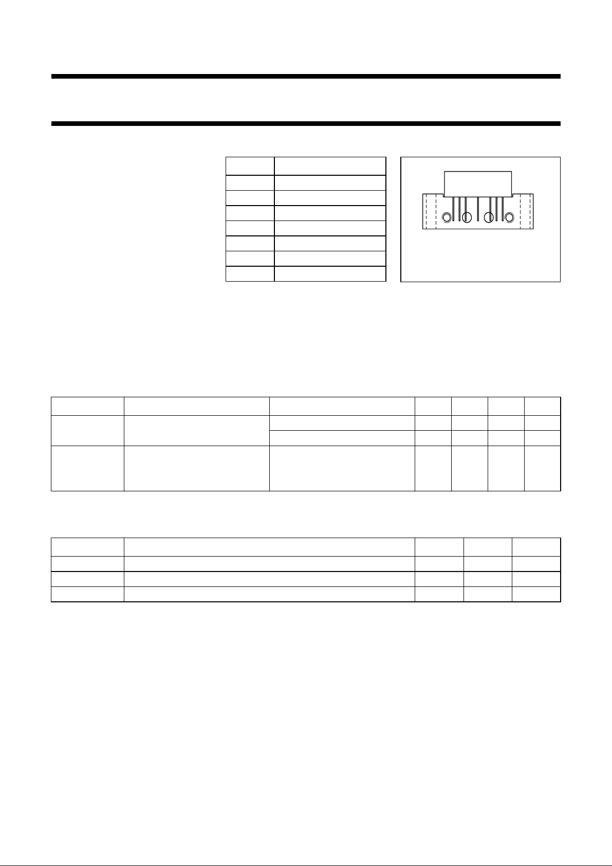
PINNING - SOT115J
PIN DESCRIPTION
1 input
2 common
3 common
5+V
B
7 common
8 common
9 output
PIN CONFIGURATION
page
2
Side view
789
351
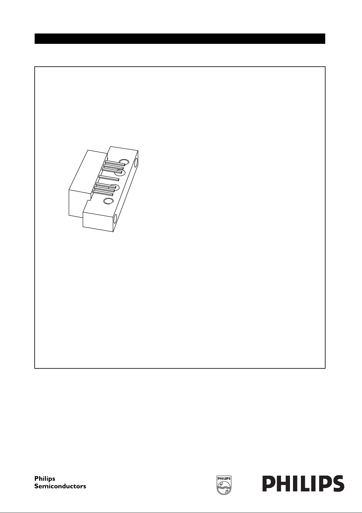
Fig.1 Simplified outline.
MSA319
Hybrid amplifier modules for CATV
systems operating over a frequency
range of 40 to 450 MHz at a voltage
supply of 24 V (DC). The BGY84 is
intended for use as an input amplifier
module and BGY85 as an output
amplifier module.
QUICK REFERENCE DATA
SYMBOL PARAMETER CONDITIONS MIN. TYP. MAX. UNIT
G
p
power gain f = 50 MHz 16.5 − 17.5 dB
f = 450 MHz 17.3 − 18.8 dB
I
tot
total current consumption (DC) VB=24V
BGY84 − 180 200 mA
BGY85 − 220 240 mA
LIMITING VALUES
In accordance with the Absolute Maximum Rating System (IEC 134).
SYMBOL PARAMETER MIN. MAX. UNIT
V
i
T
stg
T
mb
RF input voltage − 65 dBmV
storage temperature −40 +100 °C
mounting base operating temperature −20 +100 °C
1999 Mar 26 2
Philips Semiconductors Product specification
CATV amplifier modules BGY84; BGY85
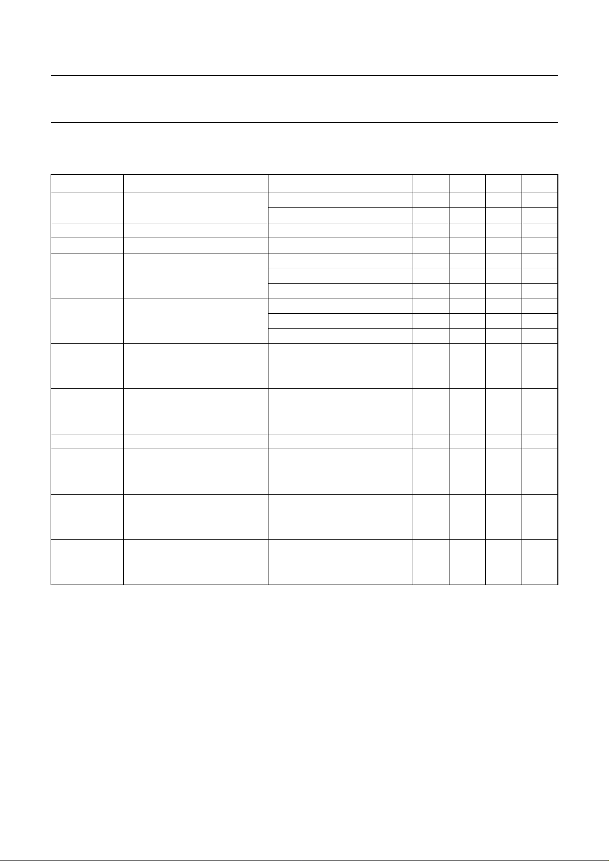
CHARACTERISTICS
Table 1 Bandwidth 40 to 450 MHz; T
=30°C; ZS=ZL=75Ω
mb
SYMBOL PARAMETER CONDITIONS MIN. TYP. MAX. UNIT
G
p
power gain f = 50 MHz 16.5 − 17.5 dB
f = 450 MHz 17.3 − 18.8 dB
SL slope cable equivalent f = 40 to 450 MHz 0.5 − 1.5 dB
FL flatness of frequency response f = 40 to 450 MHz −−±0.2 dB
S
11
input return losses f = 40 to 80 MHz 20 −−dB
f = 80 to 160 MHz 19 −−dB
f = 160 to 450 MHz 18 −−dB
S
22
output return losses f = 40 to 80 MHz 20 −−dB
f = 80 to 160 MHz 19 −−dB
f = 160 to 450 MHz 18 −−dB
CTB composite triple beat 60 channels flat; V
BGY84 −−−55 dB
measured at 445.25 MHz
= 46 dBmV;
o
BGY85 −−−58 dB
X
mod
cross modulation 60 channels flat; Vo= 46 dBmV;
BGY84 −−−57 dB
measured at 55.25 MHz
BGY85 −−−60 dB
d
2
V
o
second order distortion note 1 −−−70 dB
output voltage dim= −60 dB; note 2
BGY84 60 −−dBmV
BGY85 62.5 −−dBmV
F noise figure f = 450 MHz
BGY84 −−6.5 dB
BGY85 −−7dB
I
tot
total current consumption (DC) VB= 24 V; note 3
BGY84 − 180 200 mA
BGY85 − 220 240 mA
Notes
= 55.25 MHz; Vp= 46 dBmV;
1. f
p
fq= 343.25 MHz; Vq= 46 dBmV;
measured at fp+fq= 398.5 MHz.
2. Measured according to DIN45004B;
fp= 440.25 MHz; Vp=Vo;
fq= 447.25 MHz; Vq=Vo−6 dB;
fr= 449.25 MHz; Vr=Vo−6 dB;
measured at fp+fq−fr= 438.25 MHz.
3. The modules normally operate at VB= 24 V, but are able to withstand supply transients up to 30 V.
1999 Mar 26 3
 Loading...