

Philips bgy785ad8m DATASHEETS

DISCRETE SEMICONDUCTORS
DATA SH EET
BGY785AD/8M
CATV amplifier module
Product specification
File under Discrete Semiconductors, SC16
1997 Mar 27
Philips Semiconductors Product specification
CATV amplifier module BGY785AD/8M
FEATURES
• Excellent linearity
• Extremely low noise
• Silicon nitride passivation
• Rugged construction
• Gold metallization ensures excellent reliability.
APPLICATIONS
CATV systems operating in the 40 to 870 MHz frequency
range.
DESCRIPTION
Hybrid high dynamic range cascode amplifier module with
Darlington pre-stage dies in a SOT115J package,
operating at a voltage supply of 24 V (DC).
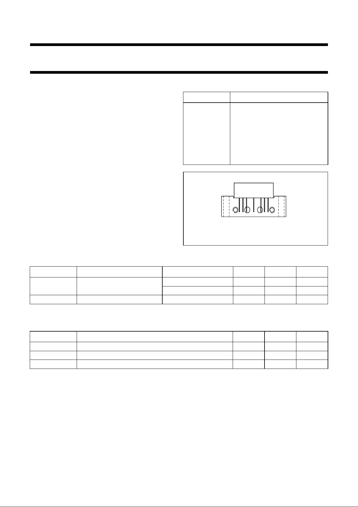
PINNING - SOT115J
PIN DESCRIPTION
1 input
2 common
3 common
5+V
7 common
8 common
9 output
handbook, halfpage
Side view
Fig.1 Simplified outline.
B
2
351
789
MSA319
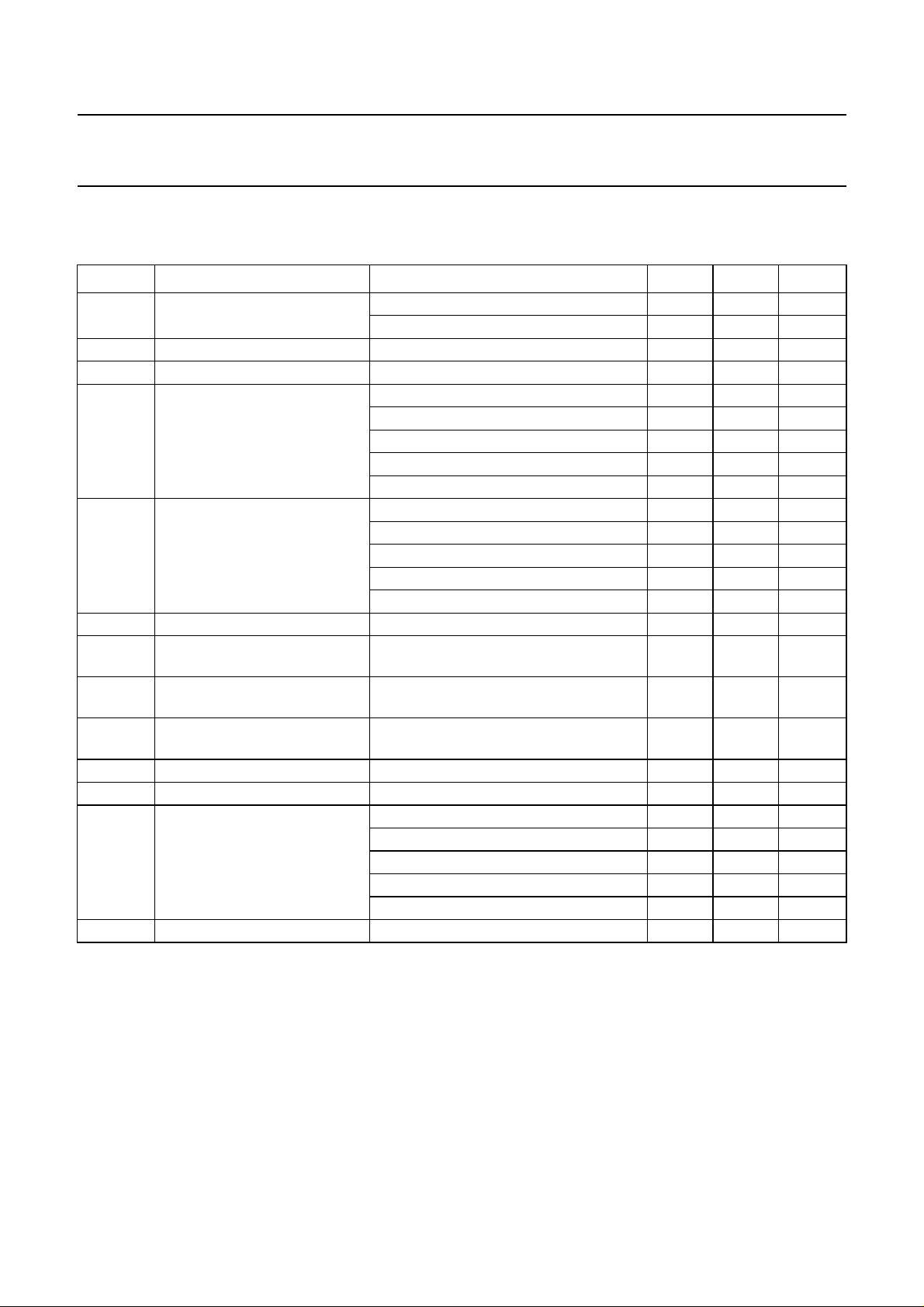
QUICK REFERENCE DATA
SYMBOL PARAMETER CONDITIONS MIN. MAX. UNIT
G
p
power gain f = 50 MHz 18 19 dB
f = 870 MHz 18.5 − dB
I
tot
total current consumption (DC) VB=24V − 265 mA
LIMITING VALUES
In accordance with the Absolute Maximum Rating System (IEC 134).
SYMBOL PARAMETER MIN. MAX. UNIT
V
i
T
stg
T
mb
RF input voltage − 60 dBmV
storage temperature −40 +100 °C
operating mounting base temperature −20 +100 °C
1997 Mar 27 2
Philips Semiconductors Product specification
CATV amplifier module BGY785AD/8M
CHARACTERISTICS
Table 1 Bandwidth 40 to 870 MHz; V
= 24 V; T
B
=30°C; ZS=ZL=75Ω
case
SYMBOL PARAMETER CONDITIONS MIN. MAX. UNIT
G
p
power gain f = 50 MHz 18 19 dB
f = 870 MHz 18.5 − dB
SL slope cable equivalent f = 40 to 870 MHz 0.2 2 dB
FL flatness of frequency response f = 40 to 870 MHz −±0.5 dB
S
11
input return losses f = 40 to 80 MHz 20 − dB
f = 80 to 160 MHz 18.5 − dB
f = 160 to 320 MHz 17 − dB
f = 320 to 640 MHz 15.5 − dB
f = 640 to 870 MHz 14 − dB
S
22
output return losses f = 40 to 80 MHz 20 − dB
f = 80 to 160 MHz 18.5 − dB
f = 160 to 320 MHz 17 − dB
f = 320 to 640 MHz 15.5 − dB
f = 640 to 870 MHz 14 − dB
S
21
CTB composite triple beat 110 channels flat, note 1;
X
mod
phase response f = 50 MHz 135 225 deg
−−58 dB
V
= 44 dBmV; measured at 745.25 MHz
o
cross modulation 110 channels flat, note 1;
−−56 dB
Vo= 44 dBmV; measured at 55.25 MHz
CSO composite second order
distortion
d
2
V
o
second order distortion notes 1 and 2 −−68 dB
output voltage dim= −60 dB; notes 1 and 3 61 − dBmV
110 channels flat, note 1
V
= 44 dBmV; measured at 746.5 MHz
o
−−58 dB
F noise figure f = 50 MHz − 5.5 dB
f = 550 MHz − 5.5 dB
f = 650 MHz − 5.5 dB
f = 750 MHz − 6dB
f = 870 MHz − 6.5 dB
I
tot
total current consumption (DC) note 4 − 265 mA
Notes
1. Linearity guaranteed up to 750 MHz.
= 55.25 MHz; Vp= 44 dBmV;
2. f
p
fq= 691.25 MHz; Vq= 44 dBmV;
measured at fp+fq= 746.5 MHz.
3. Measured according to DIN45004B:
fp= 740.25 MHz; Vp=Vo;
fq= 747.25 MHz; Vq=Vo−6 dB;
fr= 749.25 MHz; Vr=Vo−6 dB;
measured at fp+fq−fr= 738.25 MHz.
4. The module normally operates at VB= 24 V, but is able to withstand supply transients up to 30 V.
1997 Mar 27 3
 Loading...