

Philips BGY67BO Datasheet
DISCRETE SEMICONDUCTORS
DATA SH EET
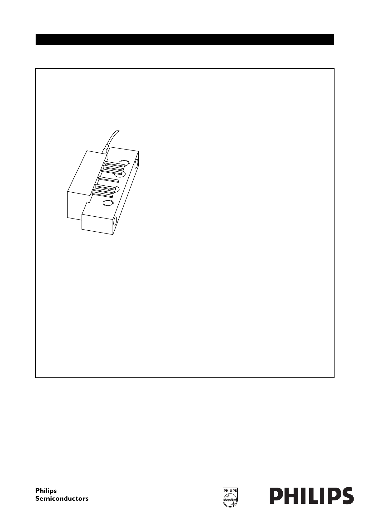
andbook, halfpage
M3D112
BGY67BO
Optical receiver module
Product specification
Supersedes data of 1997 Nov 24
File under Discrete Semiconductors, SC16
1998 Mar 13
Philips Semiconductors Product specification
Optical receiver module BGY67BO
FEATURES
• Excellent linearity
• Extremely low noise
• Excellent flatness
• Standard CATV outline
• Rugged construction
• Gold metallization ensures excellent reliability.
APPLICATIONS
• Reverse receiver amplifier in two-way CATV systems in
the 5 to 300 MHz frequency range.
DESCRIPTION
Hybrid high dynamic range optical amplifier module in a
SOT115U package operating at a voltage supply of
24 V (DC). The module contains a monomode optical
input suitable for wavelengths from 1290 to 1600 nm, a
terminal to monitor the pin diode current and an electrical
output with an impedance of 75 Ω.
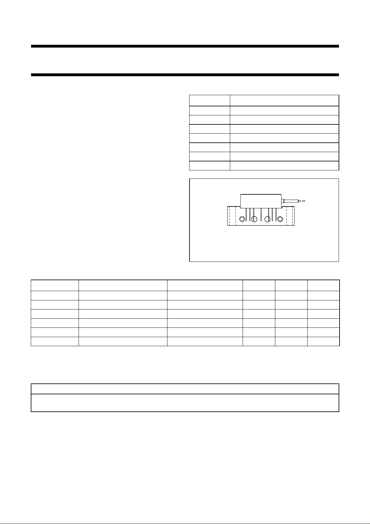
PINNING - SOT115U
PIN DESCRIPTION
1 monitor current
2 common
3 common
5+V
B
7 common
8 common
9 output
handbook, halfpage
Side view
2
789
351
Fig.1 Simplified outline.
MLB162
QUICK REFERENCE DATA
SYMBOL PARAMETER CONDITIONS MIN. MAX. UNIT
f frequency range 5 300 MHz
S
22
output return losses f = 5 to 300 MHz 15 − dB
optical input return losses 40 − dB
d
2
second order distortion −−70 dBc
F equivalent noise input f = 10 to 300 MHz − 7 pA/√Hz
I
tot
total current consumption (DC) VB= 24 V 160 190 mA
HANDLING
Fibreglass optical coupling: maximum tensile strength = 5 N; minimum bending radius = 35 mm.
CAUTION
This product is supplied in anti-static packing to prevent damage caused by electrostatic discharge during transport
and handling. For further information, refer to Philips specs.: SNW-EQ-608, SNW-FQ-302A and SNW-FQ-302B.
1998 Mar 13 2
Philips Semiconductors Product specification
Optical receiver module BGY67BO
LIMITING VALUES
In accordance with the Absolute Maximum Rating System (IEC 134).
SYMBOL PARAMETER CONDITIONS MIN. MAX. UNIT
f frequency range 5 300 MHz
T
stg
T
mb
P
in
ESD ESD sensitivity human body model;
CHARACTERISTICS
storage temperature −40 +85 °C
operating mounting base temperature −20 +85 °C
optical input power continuous − 5mW
500 − V
R = 1.5 kΩ; C = 100 pF
Table 1 Bandwidth 5 to 300 MHz; V
= 24 V; Tmb=30°C; ZL=75Ω
B
SYMBOL PARAMETER CONDITIONS MIN. MAX. UNIT
S responsivity λ = 1300 nm 800 − V/W
FL flatness of frequency response −±0.3 dB
S
22
output return losses f = 5 to 300 MHz 15 − dB
optical input return losses 40 − dB
d
2
d
3
second order distortion note 1 −−70 dB
third order distortion note 2 −−80 dB
F equivalent noise input f = 10 to 300 MHz − 7 pA/√Hz
s
λ
spectral sensitivity λ = 1310 ±20 nm 0.85 − A/W
λ = 1550 ±20 nm 0.9 − A/W
λ optical wavelength 1290 1600 nm
L length of optical fibre fibre; SM type; 9/125 µm1−m
I
tot
total current consumption (DC) note 3 160 190 mA
Notes
1. Two laser test; each laser with 40% modulation index;
fp= 20.25 MHz; Pp= 0.5 mW;
fq= 34 MHz; Pq= 0.5 mW;
measured at fp+fq= 54.25 MHz.
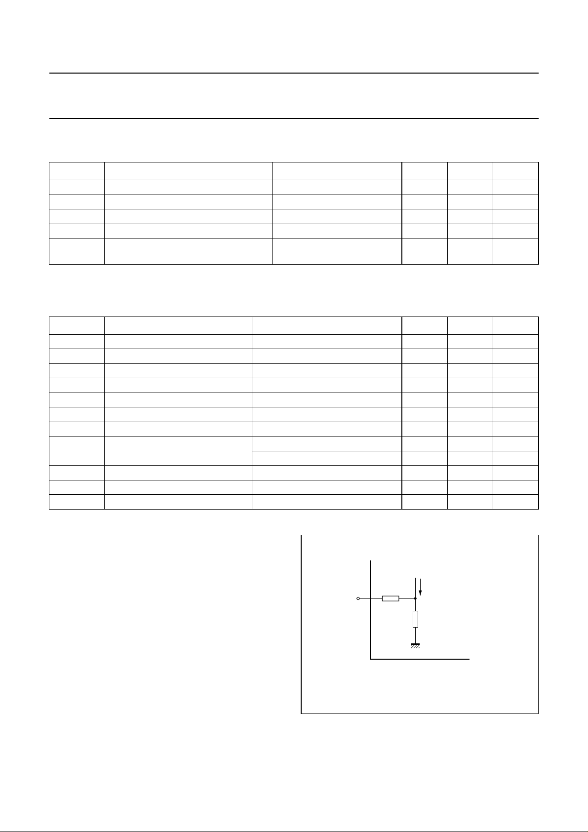
handbook, halfpage
Pin 1
10 kΩ
photo
current
2. Three laser test; each laser with 40% modulation
index;
1 kΩ
fp= 125.25 MHz; Pp= 0.33 mW;
fq= 110.25 MHz; Pq= 0.33 mW;
fr= 135.25 MHz; Pr= 0.33 mW;
measured at fp+fq−fr= 100.25 MHz.
MLB151
3. The module normally operates at VB= 24 V, but is
able to withstand supply transients up to 30 V.
Fig.2 Monitor current pin.
1998 Mar 13 3
 Loading...