

Philips BGY241 Datasheet
DISCRETE SEMICONDUCTORS
DATA SH EET
ndbook, halfpage
M3D373
BGY241
UHF amplifier module
Product specification
Supersedes data of 1999 May 01
1999 Sep 09

Philips Semiconductors Product specification
UHF amplifier module BGY241
FEATURES
• 3.5 V nominal supply voltage
• 35 dBm output power
• Easy output power control by DC voltage.
APPLICATIONS
• Digital cellularradio systems with Time Division Multiple
Access (TDMA) operation (GSM systems) in the
880 to 915 MHz frequency range.
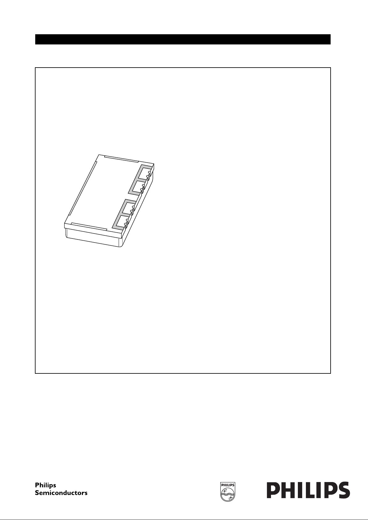
DESCRIPTION
The BGY241 is a three-stage UHF amplifier module in a
SOT482C leadless package with a plastic cover.
The module consists of one NPN silicon planar transistor
die and one bipolar monolithic integrated circuit mounted
together with matching and bias circuit components on a
metallized ceramic substrate.
QUICK REFERENCE DATA
RF performance at Tmb=25°C.
PINNING - SOT482C
PIN DESCRIPTION
1 RF input
2V
3V
C
S
4 RF output
5 ground
handbook, halfpage
43 251
Bottom view
Fig.1 Simplified outline.
MBK201
MODE OF
OPERATION
f
(MHz)
V
(V)
S
V
C
(V)
P
L
(dBm)
G
(dB)
p
η
(%)
ZS;Z
(Ω)
Pulsed; δ = 1 : 8 880 to 915 3.5 ≤2.2 35.2 ≥35.2 typ. 43 50
LIMITING VALUES
In accordance with the Absolute Maximum Rating System (IEC 134).
SYMBOL PARAMETER CONDITIONS MIN. MAX. UNIT
V
S
V
C
P
D
P
L
T
stg
T
mb
DC supply voltage VC= 0; PD=0mW − 7V
V
≥0.2 V − 5.5 V
C
DC control voltage − 2.7 V
input drive power − 10 dBm
load power − 36 dBm
storage temperature −40 +100 °C
operating mounting base temperature −30 +100 °C
CAUTION
This product is supplied in anti-static packing to prevent damage caused by electrostatic discharge during transport
and handling. For further information, refer to Philips specs.: SNW-EQ-608, SNW-FQ-302A and SNW-FQ-302B.
L
1999 Sep 09 2

Philips Semiconductors Product specification
UHF amplifier module BGY241
CHARACTERISTICS
ZS=ZL=50Ω; PD= 0 dBm; VS= 3.5 V; VC≤ 2.2 V; f = 880 to 915 MHz; Tmb=25°C; δ = 1 : 8; tp= 575 µs;
unless otherwise specified.
SYMBOL PARAMETER CONDITIONS MIN. TYP. MAX. UNIT
I
Q
I
CM
P
L
G
p
η efficiency P
H
2
H
3
VSWR
in
P
n
t
r
t
f
leakage current VC= 0.2 V; PD=0mW −−10 µA
V
=7V; VC= 0; PD=0mW − 620mA
S
peak control current PL= 35.2 dBm −−3mA
load power VC= 2.2 V 35.2 35.5 − dBm
V
=3V; VC= 2.2 V;
S
33.6 −−dBm
Tmb= −20 to +85 °C
power gain PL= 35.2 dBm − 35.2 − dB
= 34 dBm 35 42 − %
L
second harmonic PL= 35.2 dBm −−50 −38 dBc
third harmonic PL= 35.2 dBm −−53 −40 dBc
input VSWR PL=5to35dBm −−3:1
stability V
=3to5V; PD=−3 to +3 dBm;
S
−−−60 dBc
VC= 0 to 2.2 V; PL≤ 35.2 dBm;
VSWR ≤ 6 : 1 through all phases
isolation V
= 0.5 V; PD= 3 dBm −−43 −37 dBm
C
control bandwidth 1.5 −−MHz
control slope PL= −5to+5dBm − 240 − dB/V
noise power PL= 5 to 35.2 dBm;
−−76 −75 dBm
bandwidth = 100 kHz;
20 MHz above transmitter band
AM/AM conversion P
= 3% AM; f = 100 kHz;
D
− 12 14 %
PL= 5 to 35.2 dBm
AM/PM conversion P
= −0.5 to +0.5 dBm;
D
−−2 deg
PL= 5 to 35.2 dBm
T
conversion PL= 35.2 dBm; f = 915 MHz;
X/RX
− 25 30 dB
PL(925 MHz)/PD(905 MHz)
carrier rise time PL= 6 to 34 dBm; timeto settle within
−0.5 dB of final P
L
carrier fall time PL= 6 to 34 dBm; timeto settle within
ruggedness V
−0.5 dB of final P
=5V; PL= 34.8 dBm;
S
L
− 1.5 2 µs
− 1.5 2 µs
no degradation
VSWR ≤ 12 : 1 through all phases
= 4.5 V; VC= 2.3 V;
V
S
no degradation
VSWR ≤ 5 : 1 through all phases
1999 Sep 09 3

Philips Semiconductors Product specification
UHF amplifier module BGY241
handbook, halfpage
4
P
L
(W)
3
2
1
0
1 1.5 2.5
ZS=ZL=50Ω; VS= 3.5 V; PD= 1 mW;
Tmb=25°C; δ= 1 : 8; tp= 575 µs.
2
MGS648
880 MHz
915 MHz
VC (V)
Fig.2 Load power as a function of control voltage;
typical values.
880 MHz
915 MHz
5
VS (V)
MGS649
handbook, halfpage
8
P
L
(W)
6
4
2
0
234 6
ZS=ZL=50Ω; VC= 2.2 V; PD= 1 mW;
Tmb=25°C; δ = 1 : 8; tp= 575 µs.
Fig.3 Load poweras afunction of supplyvoltage;
typical values.
50
handbook, halfpage
η
(%)
40
30
20
10
0
05
ZS=ZL=50Ω; VS= 3.5 V; PD= 1 mW;
Tmb=25°C; δ= 1 : 8; tp= 575 µs.
1234
915 MHz
880 MHz
PL (W)
Fig.4 Efficiency as a function of load power;
typical values.
MGS650
handbook, halfpage
5
P
L
(W)
4
3
2
1
0
880 890 900 920910
ZS=ZL=50Ω; VS= 3.5 V; PD= 1 mW; VC= 2.2 V;
Tmb=25°C; δ= 1 : 8; tp= 575 µs.
f (MHz)
Fig.5 Load power as a function of frequency;
typical values.
MGS651
1999 Sep 09 4
 Loading...