

Philips bgy120ab DATASHEETS
DISCRETE SEMICONDUCTORS
DATA SH EET
ndbook, halfpage
M3D373
BGY120A; BGY120B
UHF amplifier modules
Objective specification
1997 Nov 11
Philips Semiconductors Objective specification
UHF amplifier modules BGY120A; BGY120B
FEATURES
• Single 3.5 V nominal supply voltage
• 1 W output power
• Easy control of output power by DC voltage
• Very high efficiency (typ. 60%)
• Silicon bipolar technology
• Standby current less than 10 µA.
APPLICATIONS
• Hand-held transmitting equipment operating in the
824 to 849 MHz and 872 to 905 MHz frequency ranges.
DESCRIPTION
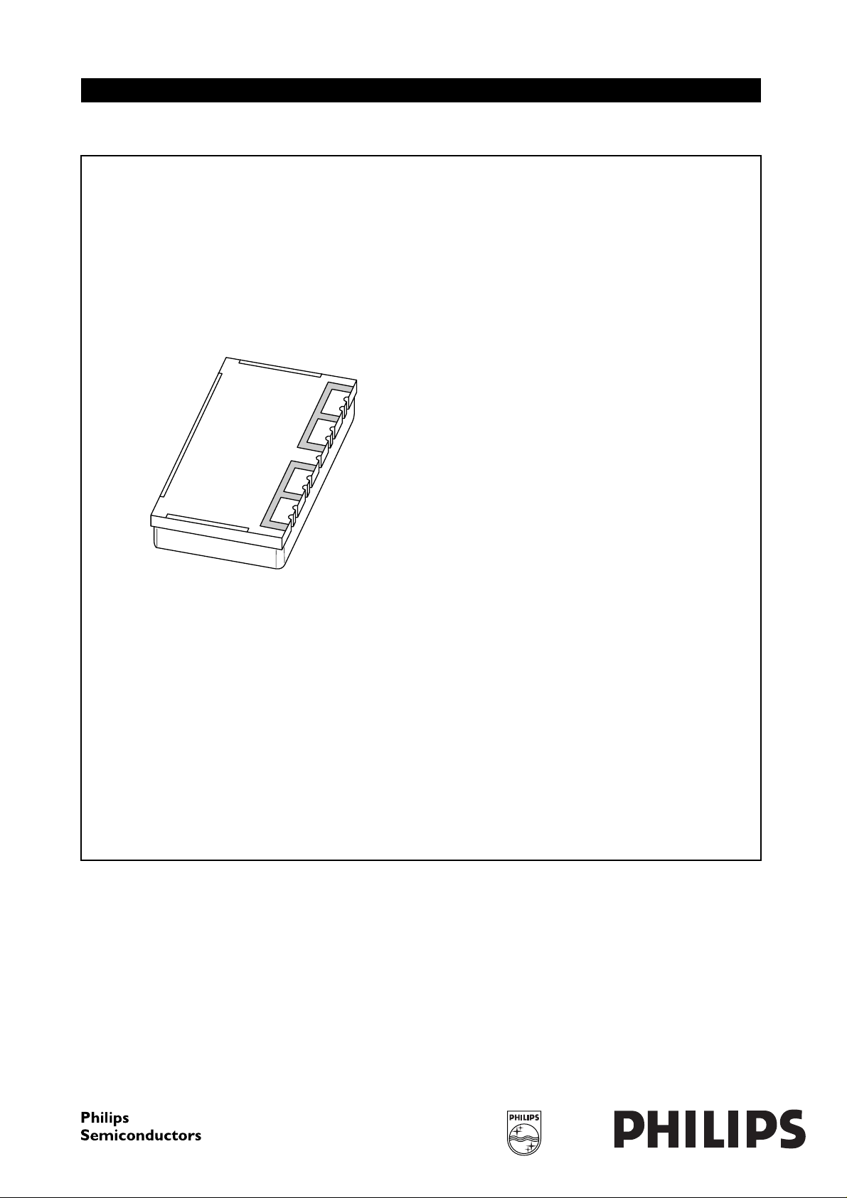
The BGY120A and BGY120B are two-stage UHF amplifier
modules in a SOT482B package with plastic cover. Each
module consists of two NPN silicon planar transistor dies
mounted together with a matching and bias circuit
components on a metallized ceramic substrate.
These modules produce an output power of 1 W into a
load of 50 Ω with an RF drive power of 5 mW.
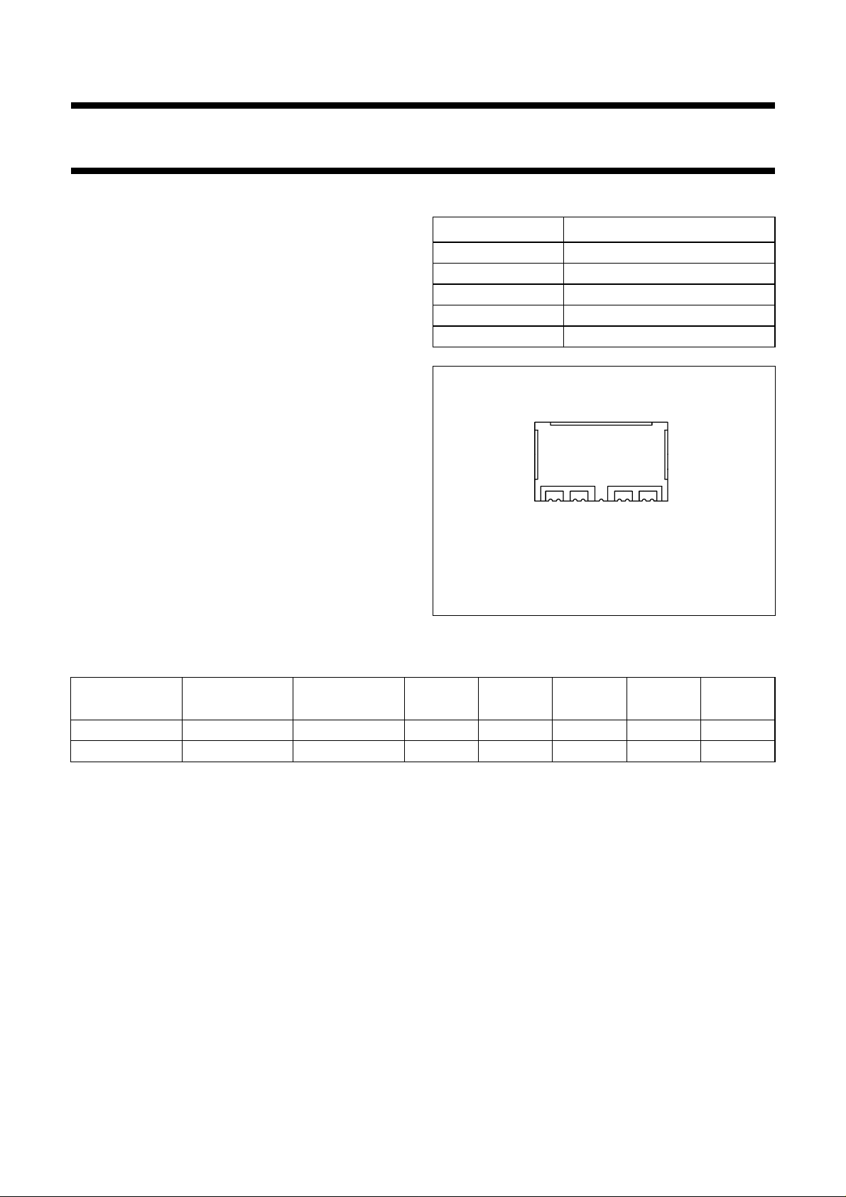
PINNING - SOT482B
PIN DESCRIPTION
1 RF input
2V
3V
4 RF output
5 flange connected to ground
handbook, halfpage
Bottom view
Fig.1 Simplified outline
C
S
43 251
MBK201
QUICK REFERENCE DATA
RF performance at T
TYPE
=25°C.
mb
MODE OF
OPERATION
f
(MHz)
V
(V)
S
P
L
(W)
G
(dB)
p
η
(%)
BGY120A CW 824 to 849 3.5 1 ≥23 typ. 60 50
BGY120B CW 872 to 905 3.5 1 ≥23 typ. 60 50
ZS; Z
(Ω)
L
1997 Nov 11 2
Philips Semiconductors Objective specification
UHF amplifier modules BGY120A; BGY120B
LIMITING VALUES
In accordance with the Absolute Maximum Rating System (IEC 134).
SYMBOL PARAMETER MIN. MAX. UNIT
V
S
V
C
P
D
P
L
T
stg
T
mb
CHARACTERISTICS
Z
S=ZL
SYMBOL PARAMETER CONDITIONS MIN. TYP. MAX. UNIT
f frequency range
I
Q
I
C
P
L
G
p
η efficiency V
H
2
H
3
VSWR
in
P
n
d
im
DC supply voltage − 5V
DC control voltage − 2.9 V
input drive power − 10 mW
load power − 1.4 W
storage temperature −40 +100 °C
operating mounting-base temperature −30 +100 °C
=50Ω; PD= 5 mW; VS= 3.5 V; VC≤ 2.5 V; Tmb=25°C; unless otherwise specified.
BGY120A 824 − 849 MHz
BGY120B 872 − 905 MHz
total leakage current VC= 0.3 V; PD< −60 dBm −−10 µA
control current −−10 mA
load power VC= 2.5 V 1 −−W
V
= 3.2 V; Tmb=85°C 0.71 −−W
S
power gain adjust VC for PL=1W 23 −−dB
= 3.2 V;
S
55 60 − %
adjust VC for PL= 0.9 W
second harmonic adjust VC for PL= 0.9 W −−−35 dBc
third harmonic adjust VC for PL= 0.9 W −−−40 dBc
input VSWR adjust VC for PL= 0.9 W −−2:1
V
≤0.5 V −−4:1
C
stability P
≤ 1.4 W; VC= 0 to 2.9 V;
L
−−−60 dBc
VS= 2.8 to 5 V; PD= 4 to 10 dBm;
VSWR ≤ 6 : 1 through all phases
isolation V
noise power adjust VC for PL=1W;
≤ 0.5 V − -40 − dBm
C
−−−90 dBm
bandwidth = 30 kHz;
fn=fo+ 45 MHz
reverse intermodulation PTx= 0.9 W; f
ruggedness V
P
int=PTx
S
− 30 dB; note 1
=5V;
int=fTx
− 45 MHz;
−−−8dB
no degradation
adjust VC for PL= 1.4 W;
VSWR ≤ 10 : 1 through all phases
Note
1. With respect to P
.
int
1997 Nov 11 3
 Loading...