

Philips BGX885N Datasheet

DISCRETE SEMICONDUCTORS
DATA SH EET
BGX885N
CATV amplifier module
Product specification
Supersedes data of 1995 Sep 14
File under Discrete Semiconductors, SC16
1997 Mar 26
Philips Semiconductors Product specification
CATV amplifier module BGX885N
FEATURES
• Excellent linearity
• Extremely low noise
• Silicon nitride passivation
• Rugged construction
• Gold metallization ensures
excellent reliability.
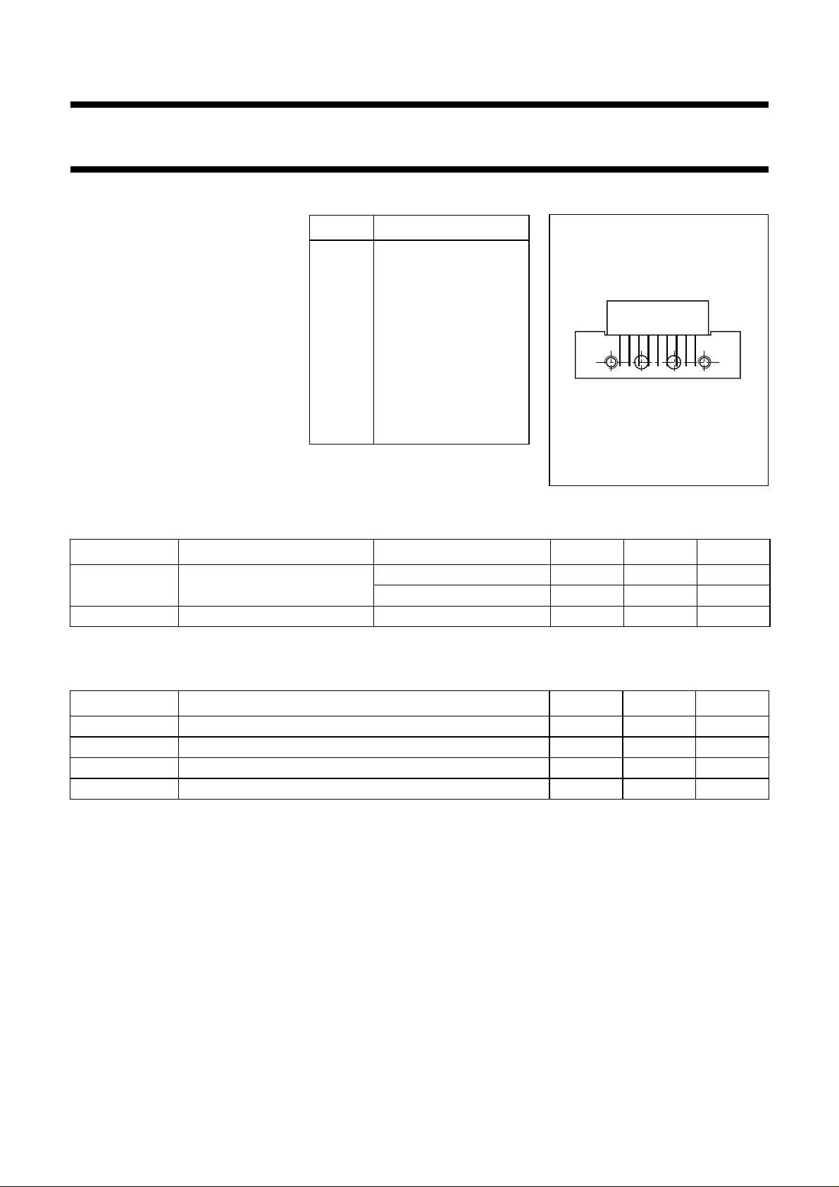
PINNING - SOT115D
PIN DESCRIPTION
1 input (note 1)
2 common
3 common
460mA
supply terminal
age
5 common
DESCRIPTION
Hybrid amplifier module for
CATV/MATV systems operating over
a frequency range of 40 to 860 MHz
6 common
7 common
8+V
B
9 output (note 1)
Side view
123 5 789
46
at a voltage supply of 24 V (DC).
Note
Fig.1 Simplified outline.
1. Pins 1 and 9 carry DC voltages.
QUICK REFERENCE DATA
SYMBOL PARAMETER CONDITIONS MIN. MAX. UNIT
G
p
power gain f = 50 MHz 16.5 17.5 dB
f = 750 MHz 17.3 − dB
I
tot
total current consumption (DC) VB= 24 V − 240 mA
MSB041 - 2
LIMITING VALUES
In accordance with the Absolute Maximum Rating System (IEC 134).
SYMBOL PARAMETER MIN. MAX. UNIT
V
B
V
i
T
stg
T
mb
DC supply voltage − 26 V
RF input voltage − 65 dBmV
storage temperature −40 +100 °C
operating mounting base temperature −20 +100 °C
1997 Mar 26 2

Philips Semiconductors Product specification
CATV amplifier module BGX885N
CHARACTERISTICS
Table 1 Bandwidth 40 to 860 MHz; V
=24V; Tmb=30°C; ZS=ZL=75Ω
B
SYMBOL PARAMETER CONDITIONS MIN. MAX. UNIT
G
p
power gain f = 50 MHz 16.5 17.5 dB
f = 750 MHz 17.3 − dB
SL slope cable equivalent f = 40 to 860 MHz 0.2 1.4 dB
FL flatness of frequency response f = 40 to 860 MHz −±0.3 dB
S
11
input return losses f = 40 MHz; note 1 20 − dB
f = 800 to 860 MHz 10 − dB
S
22
output return losses f = 40 MHz; note 1 20 − dB
f = 640 to 860 MHz 15 − dB
d
2
V
o
second order distortion note 2 −−53 dB
output voltage dim= −60 dB; note 3 61 − dBmV
d
= −60 dB; note 4 60 − dBmV
im
F noise figure f = 50 MHz − 7.5 dB
f = 350 MHz − 7.5 dB
f = 550 MHz − 7.5 dB
f = 650 MHz − 7.5 dB
f = 750 MHz − 8dB
f = 860 MHz − 8dB
I
tot
total current consumption (DC) note 5 − 240 mA
Notes
1. Decrease per octave of 1.5 dB.
= 349.25 MHz; Vp=Vo= 59 dBmV;
2. f
p
fq= 403.25 MHz; Vq=Vo;
measured at fp+fq= 752.5 MHz.
3. Measured according to DIN45004B:
fp= 341.25 MHz; Vp=Vo;
fq= 348.25 MHz; Vq=Vo−6 dB;
fr= 350.25 MHz; Vr=Vo−6 dB;
measured at fp+fq−fr= 339.25 MHz.
4. Measured according to DIN45004B:
fp= 851.25 MHz; Vp=Vo;
fq= 858.25 MHz; Vq=Vo−6 dB;
fr= 860.25 MHz; Vr=Vo−6 dB;
measured at fp+fq−fr= 849.25 MHz.
5. The module normally operates at VB= 24 V, but is able to withstand supply transients up to 30 V.
1997 Mar 26 3
 Loading...