

Philips BGO847/SC0 DATASHEETS

DISCRETE SEMICONDUCTORS
DATA SH EET
ok, halfpage
M3D456
BGO847; BGO847/FC0;
BGO847/SC0
Optical receiver modules
Product specification
Supersedes data of 2000 Jan 04
2000 Apr 12

Philips Semiconductors Product specification
Optical receiver modules
FEATURES
• Improved BGE847BO
• Excellent linearity
• Extremely lownoiseup to 870 MHz
• Excellent flatness (straight line)
• Standard CATV outline
• Rugged construction
• Gold metallization ensures
excellent reliability
• High optical input power range.
APPLICATIONS
• CATV optical node systems
operating in the 40 to 870 MHz
frequency range.
DESCRIPTION
High dynamic range optical receiver
amplifier modules in a standard
SOT115 package where the
non-jacketed fibre has either no
connector or an FC/APC or an
SC/APC connector.
The amplifier supply voltage pin and
the photo diode bias voltage pin both
connect to 24 V (DC).
The modules have a monomode
optical input suitable for
1290 to 1600 nm wavelengths, a
terminal to monitor the photo diode
current and an electrical output
having a characteristic impedance of
75 Ω.
BGO847; BGO847/FC0;
BGO847/SC0
PINNING
PIN DESCRIPTION
1 monitor current
2 common
3 common
4+V
5+V
7 common
8 common
9 output
of the photo diode
B
of the amplifier
B
e
Side view
4
2
51
3
Fig.1 Simplified outline
SOT115T
(BGO847).
789
MBK044
k, halfpage
Side view
4
2
351
Fig.2 Simplified outline
SOT115X
(BGO847/FC0).
789
MBL040
k, halfpage
Side view
24
351
Fig.3 Simplified outline
SOT115Y
(BGO847/SC0).
789
MBL041
QUICK REFERENCE DATA
SYMBOL PARAMETER CONDITIONS MIN. MAX. UNIT
f frequency range 40 870 MHz
s
22
output return losses f = 40 to 870 MHz 11 − dB
optical input return losses 45 − dB
d
2
second order distortion f = 854.5 MHz −−63 dBc
F equivalent noise input f = 40 to 750 MHz − 7 pA/√Hz
I
tot
total current consumption (DC) VB= 24 V 175 205 mA
HANDLING
Fibreglass optical coupling: maximum tensile strength = 5 N; minimum bending radius = 35 mm.
2000 Apr 12 2

Philips Semiconductors Product specification
Optical receiver modules
BGO847; BGO847/FC0;
BGO847/SC0
LIMITING VALUES
In accordance with the Absolute Maximum Rating System (IEC 134).
SYMBOL PARAMETER CONDITIONS MIN. MAX. UNIT
f frequency range 40 870 MHz
T
stg
T
mb
P
in
ESD ESD sensitivity human body model;
CHARACTERISTICS Bandwidth 40 to 870 MHz; VB= 24 V; Tmb=30°C; ZL=75Ω.
SYMBOL PARAMETER CONDITIONS MIN. MAX. UNIT
S responsivity
FL flatness straight line peak to valley; f = 40 to 870 MHz − 1dB
SL slope straight line f = 40 to 870 MHz 0 2 dB
s
22
d
2
d
3
F equivalent input noise f = 40 to 750 MHz − 7 pA/√Hz
s
λ
λ optical wavelength 1290 1600 nm
L length of optical fibre
I
tot
I
pin 4
storage temperature −40 +85 °C
operating mounting base temperature −20 +85 °C
optical input power continuous − 5mW
500 − V
R = 1.5 kΩ; C = 100 pF
BGO847 λ = 1300 nm 800 − V/W
BGO847/FC0, BGO847/SC0 λ = 1300 nm 750 − V/W
output return losses f = 40 to 870 MHz 11 − dB
optical input return losses 45 − dB
second order distortion fm= 54 MHz; notes 1 and 3 −−73 dB
f
= 446.5 MHz; notes 1 and 4 −−68 dB
m
f
= 548.5 MHz; notes 1 and 5 −−67 dB
m
f
= 746.5 MHz; notes 1 and 6 −−63 dB
m
= 854.5 MHz; notes 1 and 7 −−63 dB
f
m
third order distortion fm= 55.25 MHz; notes 2 and 8 −−80 dB
f
= 445.25 MHz; notes 2 and 9 −−75 dB
m
f
= 547.25 MHz; notes 2 and 10 −−75 dB
m
= 745.25 MHz; notes 2 and 11 −−75 dB
f
m
= 853.25 MHz; notes 2 and 12 −−73 dB
f
m
f = 750 to 870 MHz − 8 pA/√Hz
spectral sensitivity λ = 1310 ±20 nm 0.85 − A/W
λ = 1550 ±20 nm 0.9 − A/W
BGO847 fibre; SM type; 9/125 µm1−m
BGO847/FC0, BGO847/SC0 fibre; SM type; 9/125 µm 746 861 mm
total current consumption (DC) 175 205 mA
pin diode bias current (DC) − 25 mA
2000 Apr 12 3
Philips Semiconductors Product specification
Optical receiver modules
Notes
1. Two laser test; each laser with 40% modulation index; P
2. Three laser test; each laser with 60% modulation index; P
3. fm= 54 MHz; fp= 187.25 MHz; fq= 133.25 MHz.
4. fm= 446.5 MHz; fp= 97.25 MHz; fq= 349.25 MHz.
5. fm= 548 .5MHz; fp= 109.25 MHz; fq= 439.25 MHz.
6. fm= 746.5 MHz; fp= 133.25 MHz; fq= 613.25 MHz.
7. fm= 854.5 MHz; fp= 133.25 MHz; fq= 721.25 MHz.
8. fm= 55.25 MHz; fp= 109.25 MHz; fq= 133.25 MHz fr= 187.25 MHz.
9. fm= 445.25 MHz; fp= 193.25 MHz; fq= 349.25 MHz fr= 97.25 MHz.
10. fm= 547.25 MHz; fp= 217.25 MHz; fq= 439.25 MHz fr= 109.25 MHz.
11. fm= 745.25 MHz; fp= 133.25 MHz; fq= 265.25 MHz fr= 613.25 MHz.
12. fm= 853.25 MHz; fp= 133.25 MHz; fq= 265.25 MHz fr= 721.25 MHz.
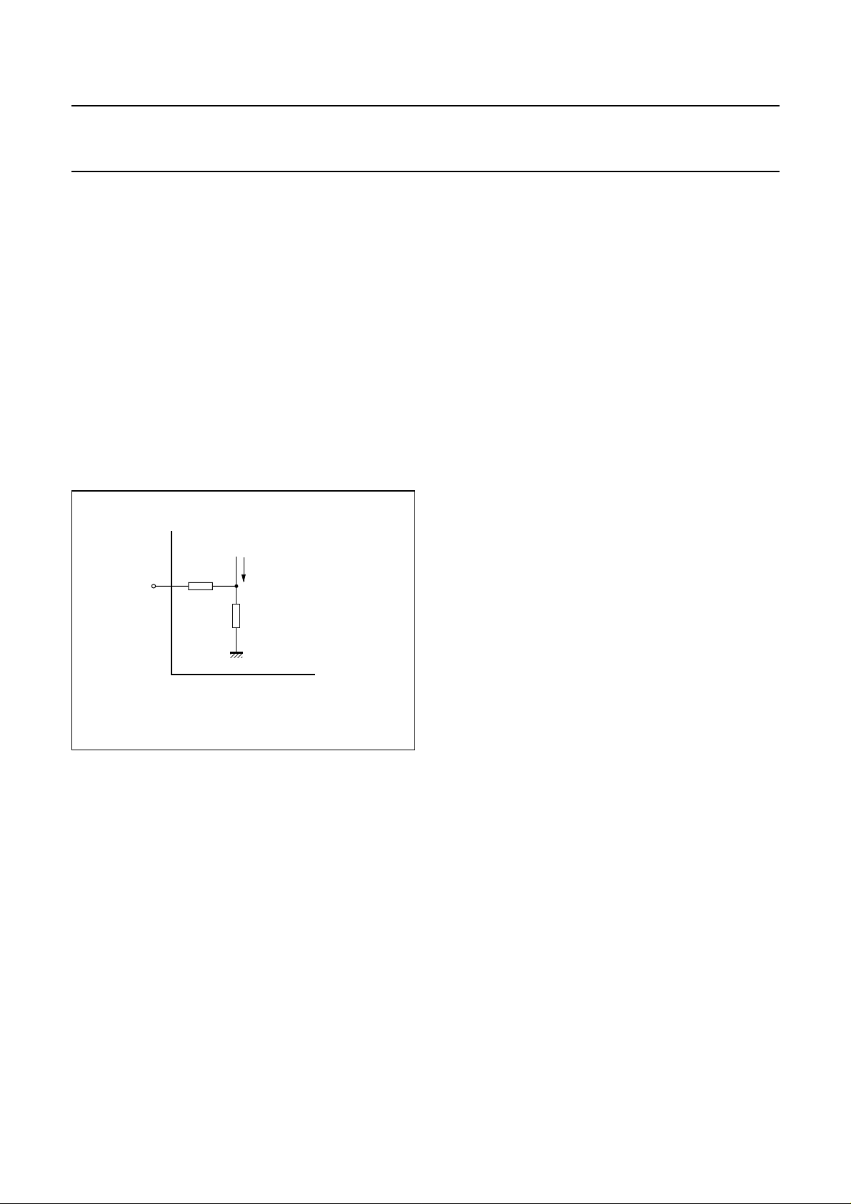
handbook, halfpage
photo
Pin 1
10 kΩ
current
= 1 mW (total).
opt
= 1 mW (total).
opt
BGO847; BGO847/FC0;
BGO847/SC0
1 kΩ
MLB151
Fig.4 Monitor current pin.
2000 Apr 12 4
 Loading...