

Philips BGD802MI, BGD802 Datasheet
DISCRETE SEMICONDUCTORS
DATA SH EET
ook, halfpage
M3D252
BGD802; BGD802MI
CATV amplifier modules
Product specification
Supersedes data of 1998 Mar 13
1999 Mar 26
Philips Semiconductors Product specification
CATV amplifier modules BGD802; BGD802MI
FEATURES
• Excellent linearity
• Extremely low noise
• Excellent return loss properties
• Silicon nitride passivation
• Rugged construction
• Gold metallization ensures excellent reliability.
APPLICATIONS
• CATV systems operating in the 40 to 860 MHz
frequency range.
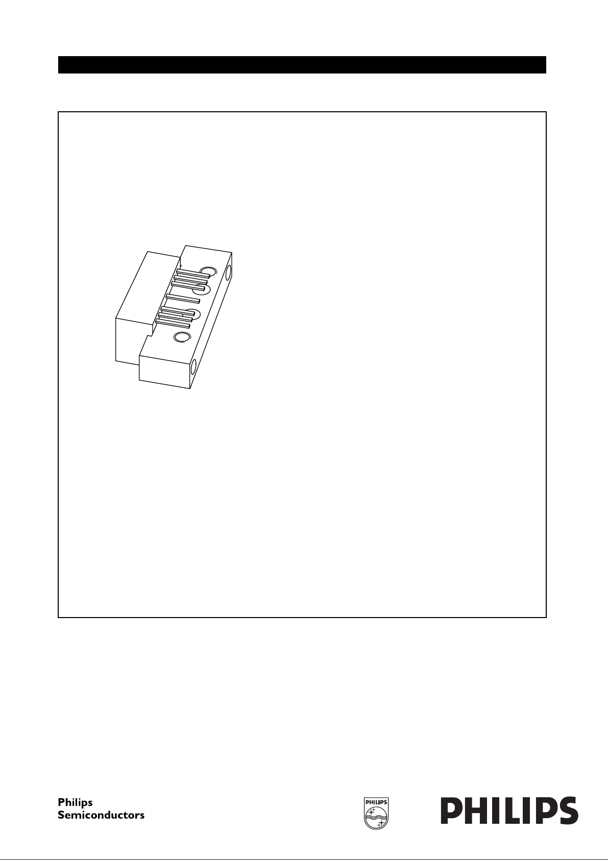
DESCRIPTION
Hybrid amplifier modules in a SOT115J package operating
with a voltage supply of 24 V (DC).
Both modules are electrically identical, only the pinning is
different.
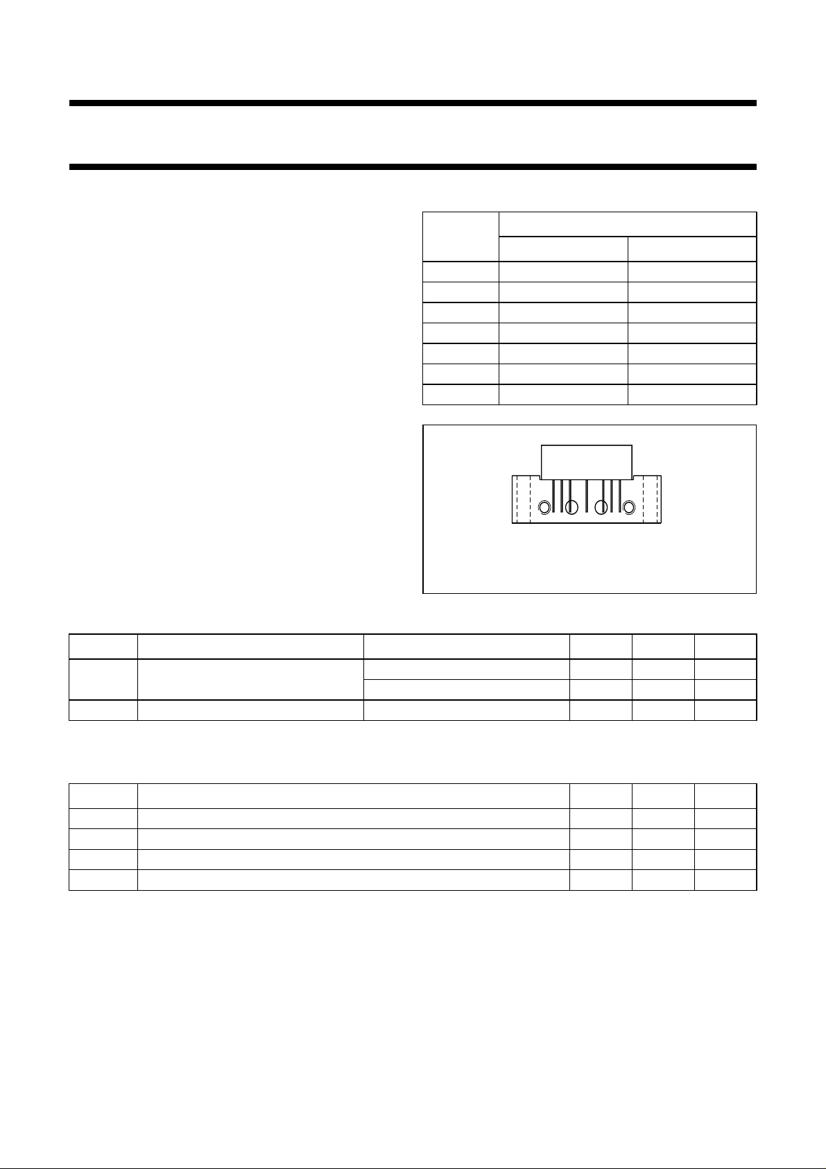
PINNING - SOT115J
DESCRIPTION
PIN
BGD802 BGD802MI
1 input output
2 common common
3 common common
5+V
B
7 common common
8 common common
9 output input
handbook, halfpage
2
Side view
789
351
Fig.1 Simplified outline.
+V
B
MSA319
QUICK REFERENCE DATA
SYMBOL PARAMETER CONDITIONS MIN. MAX. UNIT
G
p
power gain f = 50 MHz 18 19 dB
f = 860 MHz 18.5 − dB
I
tot
total current consumption (DC) VB=24V − 410 mA
LIMITING VALUES
In accordance with the Absolute Maximum Rating System (IEC 134).
SYMBOL PARAMETER MIN. MAX. UNIT
V
B
V
i
T
stg
T
mb
supply voltage − 25 V
RF input voltage − 65 dBmV
storage temperature −40 +100 °C
operating mounting base temperature −20 +100 °C
1999 Mar 26 2
Philips Semiconductors Product specification
CATV amplifier modules BGD802; BGD802MI
CHARACTERISTICS
Table 1 Bandwidth 40 to 860 MHz; V
= 24 V; T
B
=35°C; ZS=ZL=75Ω
case
SYMBOL PARAMETER CONDITIONS MIN. TYP. MAX. UNIT
G
p
power gain f = 50 MHz 18 18.5 19 dB
f = 860 MHz 18.5 19.5 − dB
SL slope cable equivalent f = 40 to 860 MHz 0.2 1.1 2 dB
FL flatness of frequency response f = 40 to 860 MHz −±0.2 ±0.5 dB
S
11
input return losses f = 40 to 80 MHz 20 35 − dB
f = 80 to 160 MHz 18.5 31 − dB
f = 160 to 320 MHz 17 27 − dB
f = 320 to 640 MHz 15.5 22 − dB
f = 640 to 860 MHz 14 20 − dB
S
22
output return losses f = 40 to 80 MHz 20 29.5 − dB
f = 80 to 160 MHz 18.5 29 − dB
f = 160 to 320 MHz 17 25.5 − dB
f = 320 to 640 MHz 15.5 23 − dB
f = 640 to 860 MHz 14 22 − dB
S
21
CTB composite triple beat 49 channels flat; V
phase response f = 50 MHz −45 − +45 deg
= 47 dBmV;
o
−−66 −63 dB
measured at 859.25 MHz
X
mod
cross modulation 49 channels flat; Vo= 47 dBmV;
−−65 −62 dB
measured at 55.25 MHz
CSO composite second order distortion 49 channels flat; V
= 47 dBmV;
o
−−67.5 −60 dB
measured at 860.5 MHz
d
2
V
o
second order distortion note 1 −−75 −69 dB
output voltage dim= −60 dB; note 2 61.5 63.5 − dBmV
F noise figure f = 50 MHz − 4.5 5.5 dB
f = 550 MHz −−6dB
f = 650 MHz −−7dB
f = 750 MHz −−7.5 dB
f = 860 MHz − 6.5 9 dB
I
tot
total current consumption (DC) note 3 − 395 410 mA
Notes
= 55.25 MHz; Vp= 44 dBmV;
1. f
p
fq= 805.25 MHz; Vq= 44 dBmV;
measured at fp+fq= 860.5 MHz.
2. Measured according to DIN45004B:
fp= 851.25 MHz; Vp=Vo;
fq= 858.25 MHz; Vq=Vo−6 dB;
fr= 860.25 MHz; Vr=Vo−6 dB;
measured at fp+fq−fr= 849.25 MHz.
3. The module normally operates at VB= 24 V, but is able to withstand supply transients up to 30 V.
1999 Mar 26 3
Philips Semiconductors Product specification
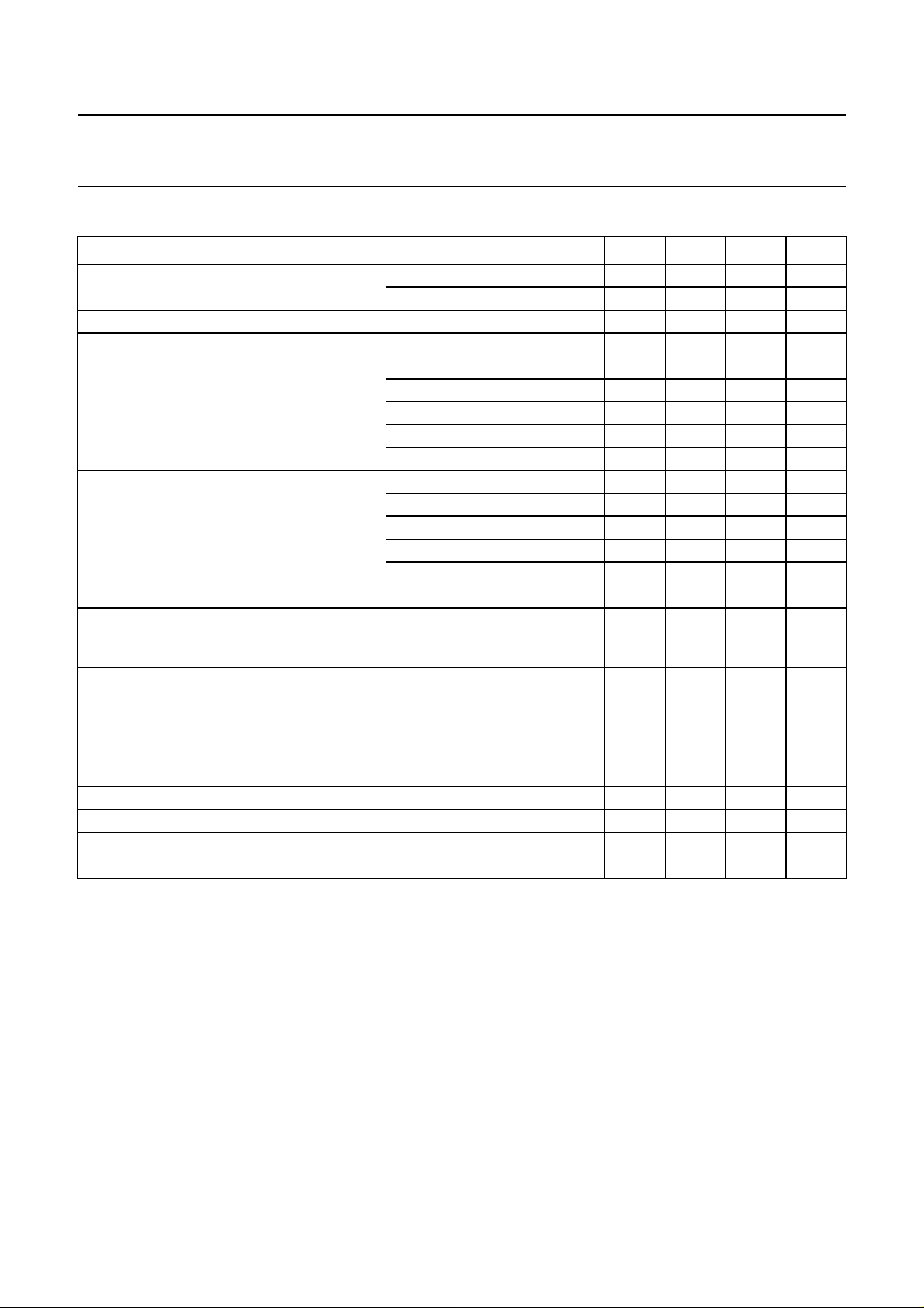
CATV amplifier modules BGD802; BGD802MI
Table 2 Bandwidth 40 to 860 MHz; VB= 24 V; T
=30°C; ZS=ZL=75Ω
case
SYMBOL PARAMETER CONDITIONS MIN. TYP. MAX. UNIT
G
p
power gain f = 50 MHz 18 18.5 19 dB
f = 860 MHz 18.5 19.5 − dB
SL slope cable equivalent f = 40 to 860 MHz 0.2 1.1 2 dB
FL flatness of frequency response f = 40 to 860 MHz −±0.2 ±0.5 dB
S
11
input return losses f = 40 to 80 MHz 20 35 − dB
f = 80 to 160 MHz 18.5 31 − dB
f = 160 to 320 MHz 17 27 − dB
f = 320 to 640 MHz 15.5 22 − dB
f = 640 to 860 MHz 14 20 − dB
S
22
output return losses f = 40 to 80 MHz 20 29.5 − dB
f = 80 to 160 MHz 18.5 29 − dB
f = 160 to 320 MHz 17 25.5 − dB
f = 320 to 640 MHz 15.5 23 − dB
f = 640 to 860 MHz 14 22 − dB
S
21
CTB composite triple beat 129 channels flat;
phase response f = 50 MHz −45 − +45 deg
−−56.5 −54 dB
V
= 44 dBmV;
o
measured at 859.25 MHz
X
mod
cross modulation 129 channels flat;
−−61 −59 dB
Vo= 44 dBmV;
measured at 55.25 MHz
CSO composite second order distortion 129 channels flat;
V
= 44 dBmV;
o
−−64.5 −56 dB
measured at 860.5 MHz
d
2
V
o
second order distortion note 1 −−75 −69 dB
output voltage dim= −60 dB; note 2 61.5 63 − dBmV
F noise figure see Table 1 −−−dB
I
tot
total current consumption (DC) note 3 − 395 410 mA
Notes
1. f
= 55.25 MHz; Vp= 44 dBmV;
p
fq= 805.25 MHz; Vq= 44 dBmV;
measured at fp+fq= 860.5 MHz.
2. Measured according to DIN45004B:
fp= 851.25 MHz; Vp=Vo;
fq= 858.25 MHz; Vq=Vo−6 dB;
fr= 860.25 MHz; Vr=Vo−6 dB;
measured at fp+fq−fr= 849.25 MHz.
3. The module normally operates at VB= 24 V, but is able to withstand supply transients up to 30 V.
1999 Mar 26 4
 Loading...