

Philips BGD704 Datasheet
DISCRETE SEMICONDUCTORS
DATA SH EET
ook, halfpage
M3D252
BGD704
CATV amplifier module
Product specification
Supersedes data of 1997 Apr 02
1999 Mar 22
Philips Semiconductors Product specification
CATV amplifier module BGD704
FEATURES
• Excellent linearity
• Extremely low noise
• Silicon nitride passivation
• Rugged construction
• Gold metallization ensures
excellent reliability.
APPLICATIONS
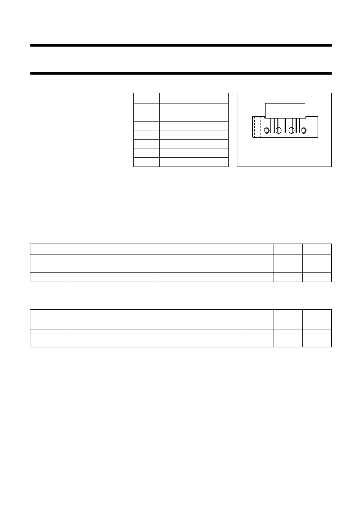
PINNING - SOT115J
PIN DESCRIPTION
1 input
2 common
3 common
5+V
B
7 common
8 common
9 output
lfpage
2
351
Side view
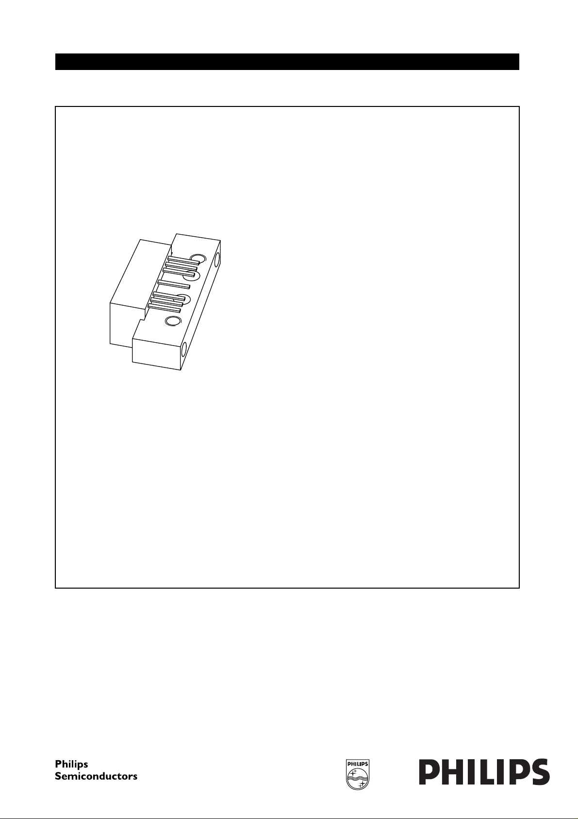
Fig.1 Simplified outline.
789
• CATV systems in the frequency
range of 40 to 750 MHz.
DESCRIPTION
Hybrid amplifier module operating at
a voltage supply of 24 V (DC)
encapsulated in a SOT115J package.
QUICK REFERENCE DATA
SYMBOL PARAMETER CONDITIONS MIN. MAX. UNIT
G
p
power gain f = 50 MHz 19.5 20.5 dB
f = 750 MHz 20 − dB
I
tot
total current consumption (DC) VB=24V − 435 mA
MSA319
LIMITING VALUES
In accordance with the Absolute Maximum Rating System (IEC 134).
SYMBOL PARAMETER MIN. MAX. UNIT
V
i
T
stg
T
mb
RF input voltage − 65 dBmV
storage temperature −40 +100 °C
operating mounting base temperature −20 +100 °C
1999 Mar 22 2
Philips Semiconductors Product specification
CATV amplifier module BGD704
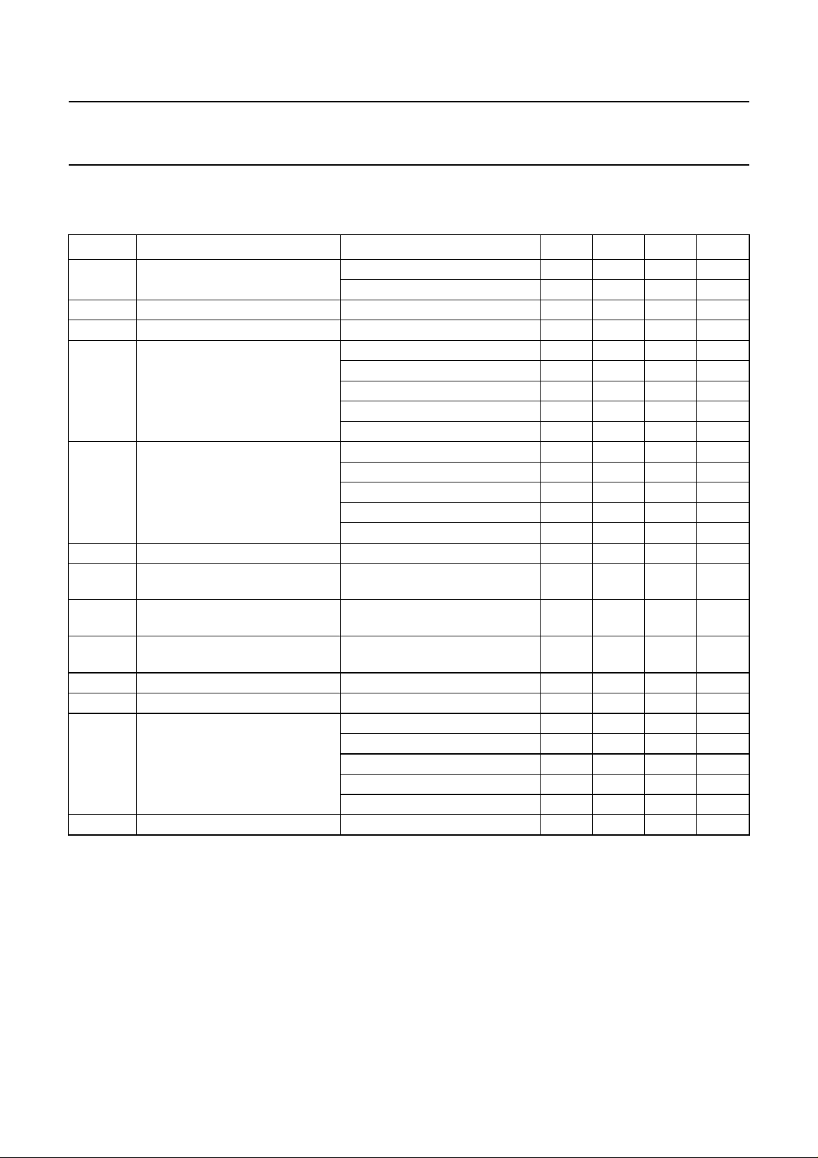
CHARACTERISTICS
Table 1 Bandwidth 40 to 750 MHz; V
= 24 V; Tmb=35°C; ZS=ZL=75Ω
B
SYMBOL PARAMETER CONDITIONS MIN. TYP. MAX. UNIT
G
p
power gain f = 50 MHz 19.5 20 20.5 dB
f = 750 MHz 20 21 − dB
SL slope cable equivalent f = 40 to 750 MHz 012dB
FL flatness of frequency response f = 40 to 750 MHz −±0.2 ±0.5 dB
S
11
input return losses f = 40 to 80 MHz 20 31 − dB
f = 80 to 160 MHz 19 29 − dB
f = 160 to 320 MHz 18 25 − dB
f = 320 to 640 MHz 17 21 − dB
f = 640 to 750 MHz 16 21 − dB
S
22
output return losses f = 40 to 80 MHz 20 26 − dB
f = 80 to 160 MHz 19 27 − dB
f = 160 to 320 MHz 18 26 − dB
f = 320 to 640 MHz 17 24 − dB
f = 640 to 750 MHz 16 23 − dB
S
21
CTB composite triple beat 110 channels flat; V
phase response f = 50 MHz −45 − +45 deg
= 44 dBmV;
o
−−58 −57 dB
measured at 745.25 MHz
X
mod
cross modulation 1 10 channels flat; Vo= 44 dBmV;
−−63 −61 dB
measured at 55.25 MHz
CSO composite second order distortion 1 10 channels flat; V
= 44 dBmV;
o
−−61 −56 dB
measured at 746.5 MHz
d
2
V
o
second order distortion note 1 −−75 −66 dB
output voltage dim= −60 dB; note 2 60.5 63.5 − dBmV
F noise figure f = 50 MHz − 4.5 5 dB
f = 450 MHz −−6.5 dB
f = 550 MHz −−7dB
f = 600 MHz −−7dB
f = 750 MHz − 6.5 8.5 dB
I
tot
total current consumption (DC) note 3 − 425 435 mA
Notes
= 55.25 MHz; Vp= 44 dBmV;
1. f
p
fq= 691.25 MHz; Vq= 44 dBmV;
measured at fp+fq= 746.5 MHz.
2. Measured according to DIN45004B:
fp= 740.25 MHz; Vp=Vo;
fq= 747.25 MHz; Vq=Vo−6 dB;
fr= 749.25 MHz; Vr=Vo−6 dB;
measured at fp+fq−fr= 738.25 MHz.
3. The module normally operates at VB= 24 V, but is able to withstand supply transients up to 30 V.
1999 Mar 22 3
Philips Semiconductors Product specification
CATV amplifier module BGD704
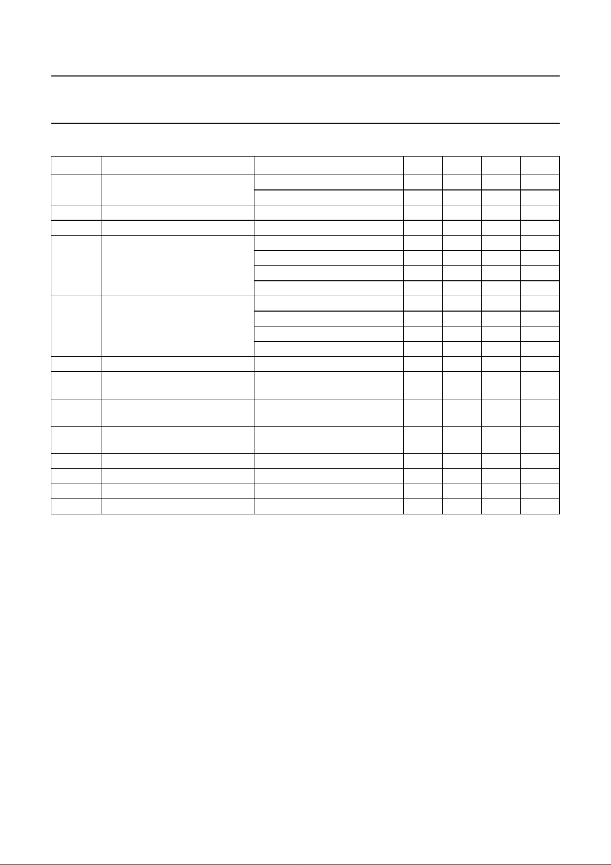
Table 2 Bandwidth 40 to 600 MHz; VB= 24 V; Tmb=35°C; ZS=ZL=75Ω
SYMBOL PARAMETER CONDITIONS MIN. TYP. MAX. UNIT
G
p
SL slope cable equivalent f = 40 to 600 MHz 0 − 2dB
FL flatness of frequency response f = 40 to 600 MHz −−±0.3 dB
S
11
S
22
S
21
CTB composite triple beat 85 channels flat; V
X
mod
CSO composite second order distortion 85 channels flat; V
d
2
V
o
F noise figure see Table 1 −−−dB
I
tot
power gain f = 50 MHz 19.5 20 20.5 dB
f = 600 MHz 20 20.7 − dB
input return losses f = 40 to 80 MHz 20 31 − dB
f = 80 to 160 MHz 19 29 − dB
f = 160 to 320 MHz 18 25 − dB
f = 320 to 600 MHz 17 21 − dB
output return losses f = 40 to 80 MHz 20 26 − dB
f = 80 to 160 MHz 19 27 − dB
f = 160 to 320 MHz 18 26 − dB
f = 320 to 600 MHz 17 24 − dB
phase response f = 50 MHz −45 − +45 deg
= 44 dBmV;
o
−−65 −64 dB
measured at 595.25 MHz
cross modulation 85 channels flat; Vo= 44 dBmV;
−−65 −64 dB
measured at 55.25 MHz
= 44 dBmV;
o
−−66 −58 dB
measured at 596.5 MHz
second order distortion note 1 −−−68 dB
output voltage dim= −60 dB; note 2 63 −−dBmV
total current consumption (DC) note 3 − 425 435 mA
Notes
1. f
= 55.25 MHz; Vp= 44 dBmV;
p
fq= 541.25 MHz; Vq= 44 dBmV;
measured at fp+fq= 596.5 MHz.
2. Measured according to DIN45004B:
fp= 590.25 MHz; Vp=Vo;
fq= 597.25 MHz; Vq=Vo−6 dB;
fr= 599.25 MHz; Vr=Vo−6 dB;
measured at fp+fq−fr= 588.25 MHz.
3. The module normally operates at VB= 24 V, but is able to withstand supply transients up to 30 V.
1999 Mar 22 4
 Loading...