

查询BGA2717供应商查询BGA2717供应商
BGA2717
MMIC wideband amplifier
Rev. 02 — 24 September 2004 Product data sheet
1. Product profile
1.1 General description
Silicon Monolithic Microwave Integrated Circuit (MMIC) wideband amplifier with internal
matching circuit in a 6-pin SOT363 SMD plastic package.
CAUTION
This device is sensitive to electrostatic discharge (ESD). Therefore care should be taken
during transport and handling.
MSC895
1.2 Features
■ Internally matched to 50 Ω
■ Wide frequency range (3.2 GHz at 3 dB bandwidth)
■ Flat 24 dB gain (±1 dB up to 2.8 GHz)
■ −2.5 dBm output power at 1 dB compression point
■ Good linearity for low current (IP3
= 10 dBm)
out
■ Low second harmonic; −38 dBc at PD = −40 dBm
■ Low noise figure; 2.3 dB at 1 GHz
■ Unconditionally stable (K ≥ 2).
1.3 Applications
■ LNB IF amplifiers
■ Cable systems
■ ISM
■ General purpose.
1.4 Quick reference data
Table 1: Quick reference data
Symbol Parameter Conditions Min Typ Max Unit
V
S
I
S
2
s
21
NF noise figure f = 1 GHz - 2.3 - dB
P
L(sat)
DC supply voltage - 5 6 V
supply current - 8 - mA
insertion power gain f = 1 GHz - 24 - dB
saturated load power f = 1 GHz - 1 - dBm
Philips Semiconductors
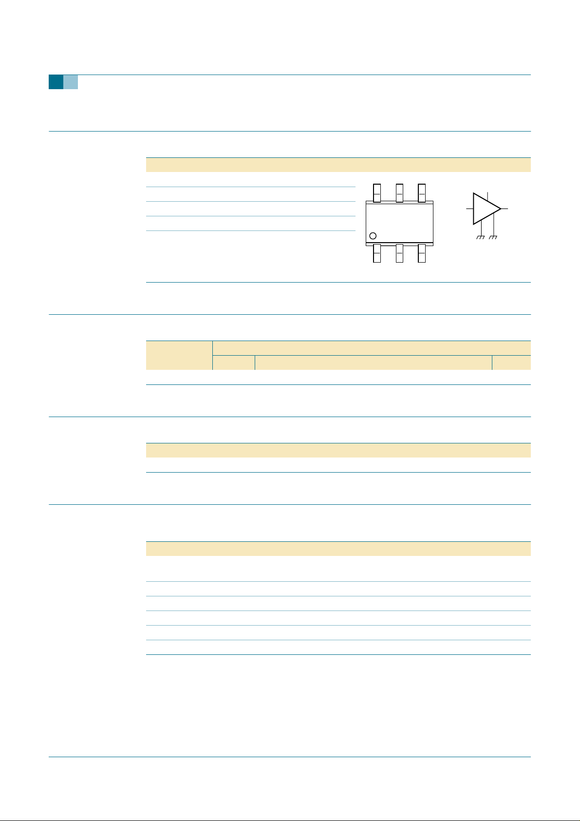
2. Pinning information
Table 2: Pinning
Pin Description Simplified outline Symbol
1V
2, 5 GND2
3 RF_OUT
4 GND1
6 RF_IN
3. Ordering information
Table 3: Ordering information
Type number Package
BGA2717 - plastic surface mounted package; 6 leads SOT363
BGA2717
MMIC wideband amplifier
S
132
56
SOT363
4
Name Description Version
1
6
4
3
2, 5
sym052
4. Marking
Table 4: Marking
Type number Marking code
BGA2717 1B-
5. Limiting values
Table 5: Limiting values
In accordance with the Absolute Maximum Rating System (IEC 60134).
Symbol Parameter Conditions Min Max Unit
V
S
I
S
P
tot
T
stg
T
j
P
D
DC supply voltage RF input AC
-6V
coupled
supply current - 15 mA
total power dissipation Tsp≤ 90 °C - 200 mW
storage temperature −65 +150 °C
junction temperature - 150 °C
maximum drive power - −10 dBm
9397 750 13293 © Koninklijke Philips Electronics N.V. 2004. All rights reserved.
Product data sheet Rev. 02 — 24 September 2004 2 of 14

Philips Semiconductors
6. Thermal characteristics
Table 6: Thermal characteristics
Symbol Parameter Conditions Typ Unit
R
th(j-sp)
thermal resistance from junction
to solder point
7. Characteristics
Table 7: Characteristics
VS = 5 V; IS = 8 mA; Tj = 25°C; measured on demo board; unless otherwise specified.
Symbol Parameter Conditions Min Typ Max Unit
I
S
s
21
s
11
s
22
s
12
NF noise figure f = 1 GHz - 2.3 2.5 dB
B bandwidth at s21
K stability factor f = 1 GHz - 13 -
P
L(sat)
P
L(1dB)
IM2 second order
IP3
in
IP3
out
supply current 6 8 10 mA
2
insertion power
gain
2
input return
losses
2
output return
losses
2
isolation f = 1.6 GHz 54 55 - dB
saturated load
power
load power at 1 dB gain compression;
intermodulation
product
input, third
order intercept
point
output, third
order intercept
point
BGA2717
MMIC wideband amplifier
P
= 200 mW;
tot
T
≤ 90 °C
sp
f = 100 MHz 18 18.6 20 dB
f = 1 GHz 23 23.9 25 dB
f = 1.8 GHz 24 25 27 dB
f = 2.2 GHz 24 25.1 27 dB
f = 2.6 GHz 22 24 26 dB
f = 3 GHz 20 22.1 24 dB
f = 1 GHz 15 19 - dB
f = 2.2 GHz 8 9.4 - dB
f = 1 GHz 8 10 - dB
f = 2.2 GHz 5 6.8 - dB
f = 2.2 GHz 38 39 - dB
f = 2.2 GHz - 2.9 3.1 dB
2
−3 dB below flat
3 3.2 - GHz
gain at 1 GHz
f = 2.2 GHz - 1.7 f = 1 GHz 0 1.4 - dBm
f = 2.2 GHz −1 +0.1 - dBm
−4 −2.6 - dBm
f = 1 GHz
at 1 dB gain compression;
−5 −3.1 - dBm
f = 2.2 GHz
= −40 dBm;
at P
D
f
= 1 GHz
0
36 38 - dBc
f = 1 GHz −15 −13.9 - dBm
f = 2.2 GHz −20 −18.8 - dBm
f = 1 GHz 9 10 - dBm
f = 2.2 GHz 4 6.3 - dBm
300 K/W
9397 750 13293 © Koninklijke Philips Electronics N.V. 2004. All rights reserved.
Product data sheet Rev. 02 — 24 September 2004 3 of 14
Philips Semiconductors
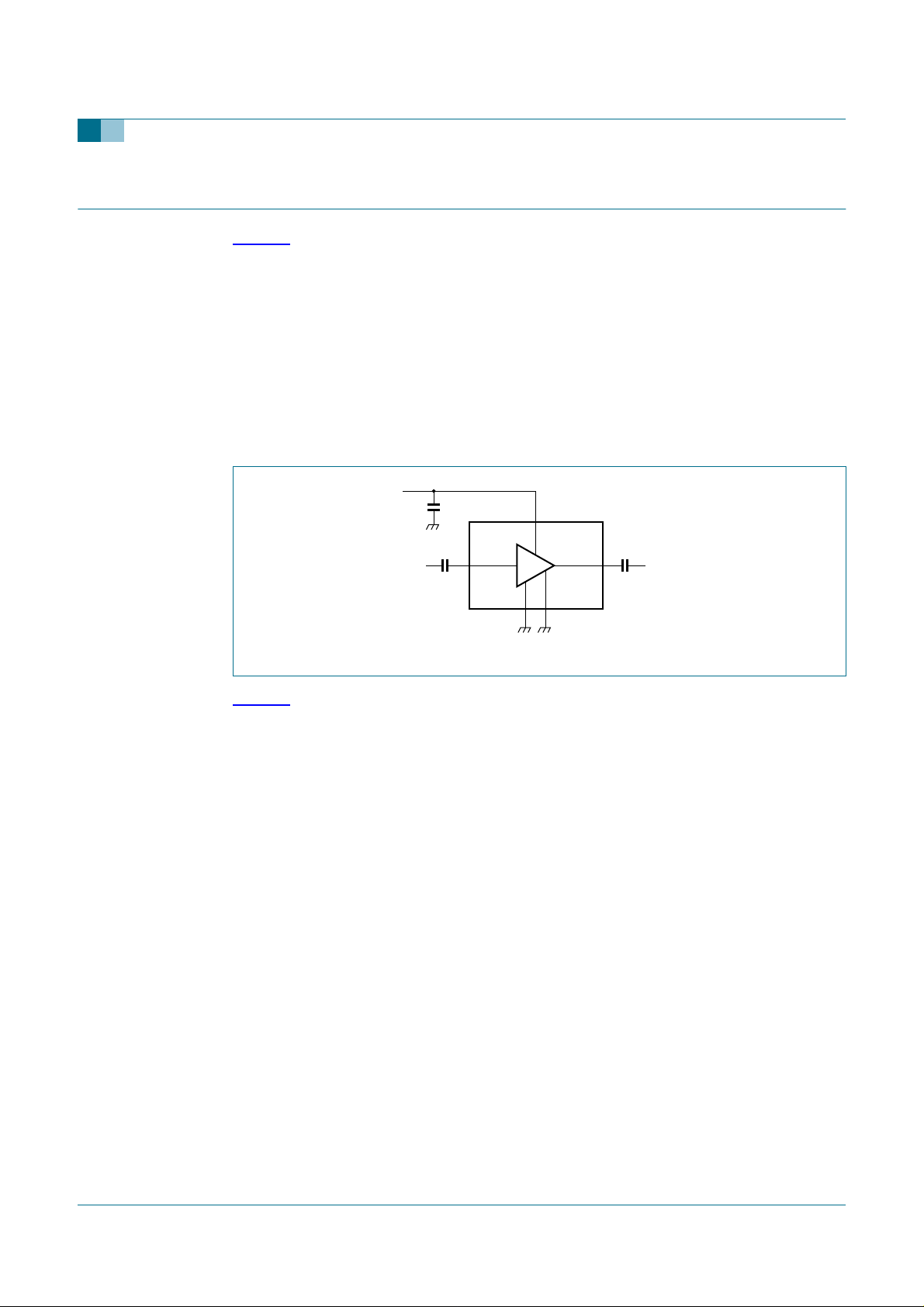
8. Application information
Figure 1 shows a typical application circuit for the BGA2717 MMIC. The device is
internally matchedto 50 Ω, and thereforedoes not need any external matching. The value
of the input and output DC blocking capacitors C2 and C3 should not be more than 100 pF
for applications above 100 MHz. However, when the device is operated below 100 MHz,
the capacitor value should be increased.
The 22 nF supply decoupling capacitor C1 should be located as close as possible to the
MMIC.
The printed-circuit board (PCB) topground plane, connectedto pins 2, 4 and 5 must beas
close as possible to the MMIC, and ideally directly beneath it. When using via holes, use
multiple via holes, located as close as possible to the MMIC.
MMIC wideband amplifier
V
S
RF input RF output
C1
C2 C3
6
1
V
S
RF_OUTRF_IN
3
BGA2717
GND2GND1
2, 5
4
mgu435
Fig 1. Typical application circuit.
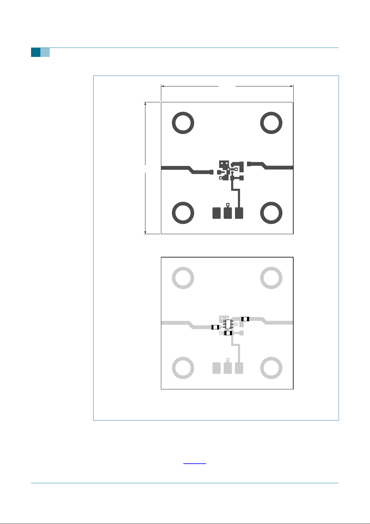
Figure 2 shows the PCB layout, used for the standard demonstration board.
9397 750 13293 © Koninklijke Philips Electronics N.V. 2004. All rights reserved.
Product data sheet Rev. 02 — 24 September 2004 4 of 14
Philips Semiconductors
BGA2717
MMIC wideband amplifier
30 mm
30 mm
PH
PH
C2
DUT
PHILIPS
OUTIN
V+
PHILIPS
C3
C1
OUTIN
V+
001aab255
Material = FR4; thickness = 0.6 mm, εr = 4.6.
Fig 2. PCB layout and demonstration board showing components.
8.1 Grounding and output impedance
If the grounding is not optimal, the gain becomes less flat and the 50 Ω output matching
becomes worse. If a better output matching to 50 Ω is required, a 12 Ω resistor (R1) can
be placed in series with C3 (see Figure 3). This will significantly improve the output
impedance, at the cost of 1 dB gain and 1 dB output power.
9397 750 13293 © Koninklijke Philips Electronics N.V. 2004. All rights reserved.
Product data sheet Rev. 02 — 24 September 2004 5 of 14
 Loading...