

Philips BFR53 Datasheet

DISCRETE SEMICONDUCTORS
DATA SH EET
BFR53
NPN 2 GHz wideband transistor
Product specification
Supersedes data of September 1995
File under Discrete Semiconductors, SC14
1997 Oct 28
Philips Semiconductors Product specification
NPN 2 GHz wideband transistor BFR53
FEATURES
• Very low intermodulation distortion
• Very high power gain.
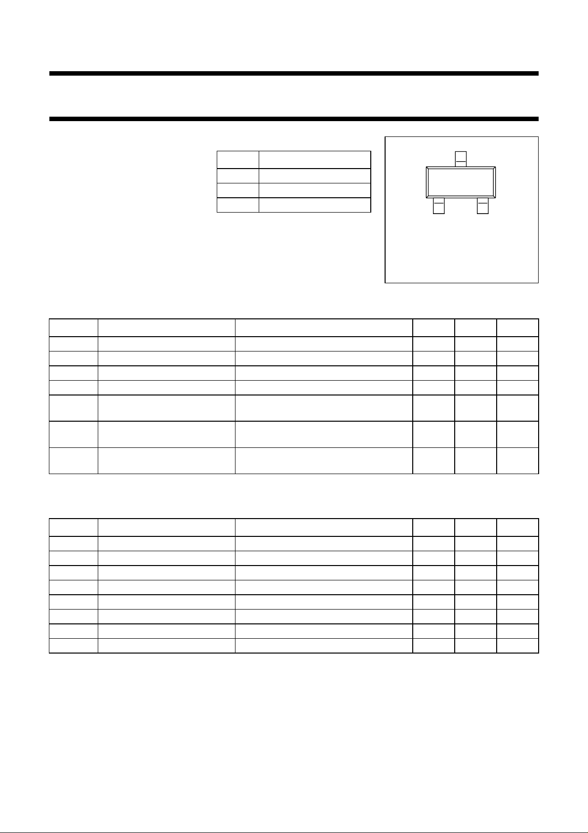
PINNING
PIN DESCRIPTION
1 base
page
3
2 emitter
APPLICATIONS
• Thick and thin-film circuits.
3 collector
12
Top view
Marking code: N1.
MSB003
DESCRIPTION
NPN wideband transistor in a plastic
Fig.1 SOT23.
SOT23 package.
QUICK REFERENCE DATA
SYMBOL PARAMETER CONDITIONS TYP. MAX. UNIT
V
V
I
P
C
f
G
CBO
CEO
CM
tot
re
T
UM
collector-base voltage open emitter − 18 V
collector-emitter voltage open base − 10 V
peak collector current f > 1 MHz − 100 mA
total power dissipation Ts≤ 85 °C − 250 mW
feedback capacitance IC= 2 mA; VCE= 5 V; f = 1 MHz;
T
=25°C
amb
transition frequency IC= 25 mA; VCE= 5 V; f = 500 MHz;
=25°C
T
j
maximum unilateral power gain IC= 30 mA; VCE= 5 V; f = 800 MHz;
T
=25°C
amb
0.9 − pF
2 − GHz
10.5 − dB
LIMITING VALUES
In accordance with the Absolute Maximum Rating System (IEC 134).
SYMBOL PARAMETER CONDITIONS TYP. MAX. UNIT
V
V
V
I
I
P
T
T
CBO
CEO
EBO
C
CM
tot
stg
j
collector-base voltage open emitter − 18 V
collector-emitter voltage open base − 10 V
emitter-base voltage open collector − 2.5 V
collector current (DC) − 50 mA
peak collector current f > 1 MHz − 100 mA
total power dissipation Ts≤ 85 °C (note 1) − 250 mW
storage temperature −65 +150 °C
junction temperature − 150 °C
Note
is the temperature at the soldering point of the collector pin.
1. T
s
1997 Oct 28 2

Philips Semiconductors Product specification
NPN 2 GHz wideband transistor BFR53
THERMAL CHARACTERISTICS
SYMBOL PARAMETER CONDITIONS VALUE UNIT
R
th j-s
Note
1. T
s
CHARACTERISTICS
=25°C unless otherwise specified.
T
j
SYMBOL PARAMETER CONDITIONS MIN. TYP. MAX. UNIT
I
CBO
h
FE
C
c
C
e
C
re
f
T
G
UM
F noise figure I
thermal resistance from junction to soldering point Ts≤ 85 °C; note 1 260 K/W
is the temperature at the soldering point of the collector pin.
collector cut-off current IE= 0; VCB=10V −−50 nA
DC current gain IC= 25 mA; VCE= 5 V; see Fig.2 25 −−
I
= 50 mA; VCE= 5 V; see Fig.2 25 −−
C
collector capacitance IE=ie= 0; VCB= 5 V; f = 1 MHz;
− 0.9 − pF
see Fig.3
emitter capacitance IC=ic= 0; VEB= 0.5 V; f = 1 MHz − 1.5 − pF
feedback capacitance IC= 2 mA; VCE= 5 V; f = 1 MHz;
T
=25°C
amb
transition frequency IC= 25 mA; VCE= 5 V; f = 500 MHz;
− 0.9 − pF
− 2 − GHz
see Fig.4
maximum unilateral power gain
(note 1)
IC= 30 mA; VCE= 5 V; f = 800 MHz;
T
=25°C; see Fig.5
amb
= 2 mA; VCE= 5 V; f = 500 MHz;
C
T
=25°C; see Fig.6
amb
− 10.5 − dB
−−5dB
Note
1. G
2
S
=
is the maximum unilateral power gain, assuming S12 is zero and .
UM
GUM10 log
--------------------------------------------------------------
1S
–
21
2
1S
–
11
22
˙
dB
2
1997 Oct 28 3
Philips Semiconductors Product specification
NPN 2 GHz wideband transistor BFR53
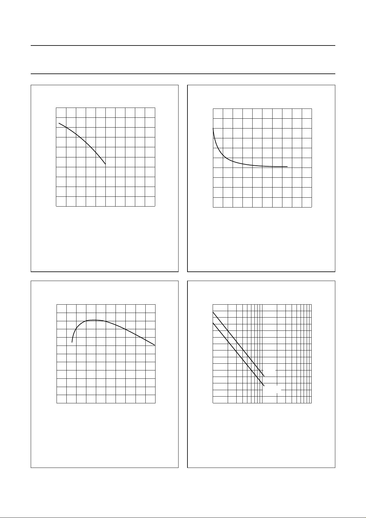
I (mA)
C
MEA458
100
handbook, halfpage
h
FE
90
80
70
60
50
0
VCE= 5V; Tj=25°C.
50 100
Fig.2 DC current gain as a function of collector
current; typical values.
2.0
handbook, halfpage
C
c
(pF)
1.6
1.2
0.8
0.4
0
016
IE=ie= 0; f = 1 MHz; Tj=25°C.
4
812
V
Fig.3 Collector capacitance as a function of
collector-base voltage; typical values.
CB
MEA457
20
(V)
2.2
handbook, halfpage
f
T
(GHz)
1.8
1.4
1.0
0
VCE= 5 V; f = 500 MHz; Tj=25°C.
25
I (mA)
C
Fig.4 Transition frequency as a function of
collector current; typical values.
MEA459
f (MHz)
MEA455
4
10
30
handbook, halfpage
gain
(dB)
20
10
=25°C.
G
UM
I S I
12
3
2
10
0
50
IC= 30 mA; VCE= 5 V; T
2
10
amb
Fig.5 Gain as a function of frequency;
typical values.
1997 Oct 28 4
 Loading...