

Philips BFQ67T Datasheet

DISCRETE SEMICONDUCTORS
M3D173
DATA SHEET
BFQ67T
NPN 8 GHz wideband transistor
Preliminary specification 1999 Oct 18
Philips Semiconductors Preliminary specification
NPN 8 GHz wideband transistor BFQ67T
FEATURES
• High power gain
• Low noise figure
• High transition frequency
• Gold metallization ensures
excellent reliability
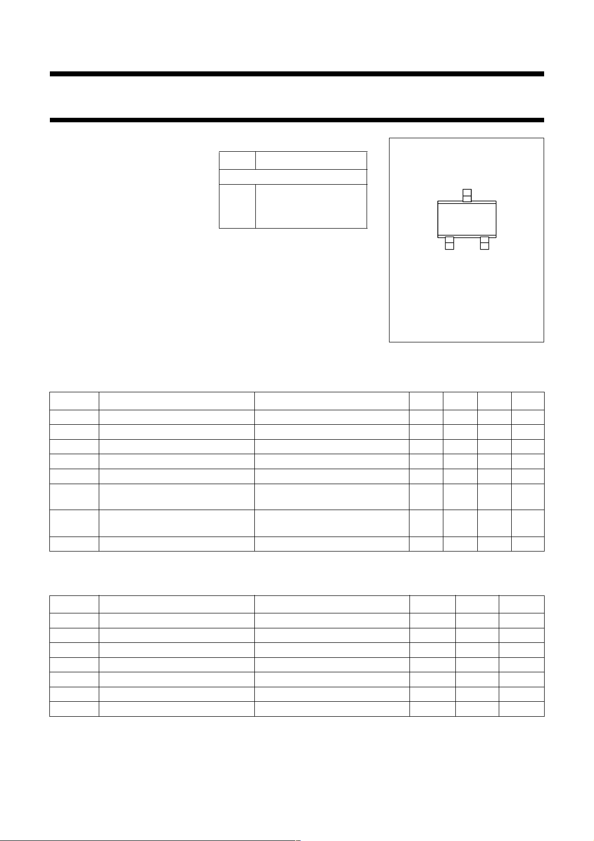
PINNING
PIN DESCRIPTION
Code: V2
1 base
2 emitter
3 collector
handbook, 2 columns
3
• SOT416 (SC75) envelope.
12
DESCRIPTION
Top view
MBC870
NPN transistor in a plastic SOT416
(SC75) envelope.
It is designed for wideband
applications such as satellite TV
tuners and RF portable
Fig.1 SOT416.
communications equipment up to
2GHz.
QUICK REFERENCE DATA
SYMBOL PARAMETER CONDITIONS MIN. TYP. MAX. UNIT
V
CBO
V
CEO
I
C
P
tot
h
FE
f
T
G
UM
F noise figure I
collector-base voltage open emitter −−20 V
collector-emitter voltage open base −−10 V
DC collector current −−50 mA
total power dissipation up to Ts= 118 °C; note 1 −−300 mW
DC current gain IC=15 mA; VCE=5 V; Tj= 25 °C 60 100 −
transition frequency IC=15 mA; VCE=8 V; f =2 GHz;
= 25 °C
T
amb
maximum unilateral power gain Ic= 15 mA; VCE=8 V; f =1 GHz;
T
= 25 °C
amb
=5 mA; VCE=8 V; f=1 GHz − 1.3 − dB
c
− 8 − GHz
− 13 − dB
LIMITING VALUES
In accordance with the Absolute Maximum System (IEC 134).
SYMBOL PARAMETER CONDITIONS MIN. MAX. UNIT
V
V
V
I
P
T
T
CBO
CEO
EBO
C
tot
stg
j
collector-base voltage open emitter − 20 V
collector-emitter voltage open base − 10 V
emitter-base voltage open collector − 2.5 V
DC collector current − 50 mA
total power dissipation up to Ts= 118 °C; note 1 − 300 mW
storage temperature −65 150 °C
junction temperature − 175 °C
Note
is the temperature at the soldering point of the collector tab.
1. T
s
1999 Oct 18 2

Philips Semiconductors Preliminary specification
NPN 8 GHz wideband transistor BFQ67T
THERMAL RESISTANCE
SYMBOL PARAMETER CONDITIONS THERMAL RESISTANCE
R
th j-s
Note
1. T
is the temperature at the soldering point of the collector tab.
s
CHARACTERISTICS
T
=25 °C, unless otherwise specified.
j
SYMBOL PARAMETER CONDITIONS MIN. TYP. MAX. UNIT
I
CBO
h
FE
C
c
C
e
C
re
f
T
G
UM
F noise figure Γ
thermal resistance from junction to
up to Ts= 118 °C; note 1 190 K/W
soldering point
collector cut-off current IE=0; VCB=5 V −−50 nA
DC current gain IC=15 mA; VCE= 5 V 60 100 −
collector capacitance IE=ie= 0; VCB=8 V; f=1 MHz − 0.7 − pF
emitter capacitance IC=ic= 0; VEB=0.5 V; f=1 MHz − 1.3 − pF
feedback capacitance IC=0; VCB=8 V; f=1 MHz − 0.5 − pF
transition frequency IC=15 mA; VCE=8 V; f=2 GHz;
= 25 °C
T
amb
maximum unilateral power gain
(note 1)
IC=15 mA; VCE=8 V; f=1 GHz
T
= 25 °C
amb
=15 mA; VCE=8 V; f=2 GHz;
I
C
T
= 25 °C
amb
= Γ
s
= 5 mA; VCE=8 V;
opt;IC
− 8 − GHz
− 13 − dB
− 8 − dB
− 1.3 − dB
f=1GHz
= Γ
Γ
s
=15 mA; VCE=8 V;
opt;IC
− 2 − dB
f=1GHz
Γ
= Γ
s
= 5 mA; VCE=8 V;
opt;IC
− 2.2 − dB
f=2GHz
= 5 mA; VCE=8 V;
I
C
f=2 GHz; Z
Γ
= Γ
s
opt;IC
= 60 Ω
s
=15 mA; VCE=8 V;
− 2.5 − dB
− 2.7 − dB
f=2GHz
= 5 mA; VCE=8 V;
I
C
f=2 GHz; Z
= 60 Ω
s
− 3 − dB
Note
1. G
is the maximum unilateral power gain, assuming S12is zero and
UM
2
S
G
UM
10 log
---------------------- ------------- -------------------- --- dB.=
1S
–()1S
21
2
11
2
–()
22
1999 Oct 18 3
Philips Semiconductors Preliminary specification
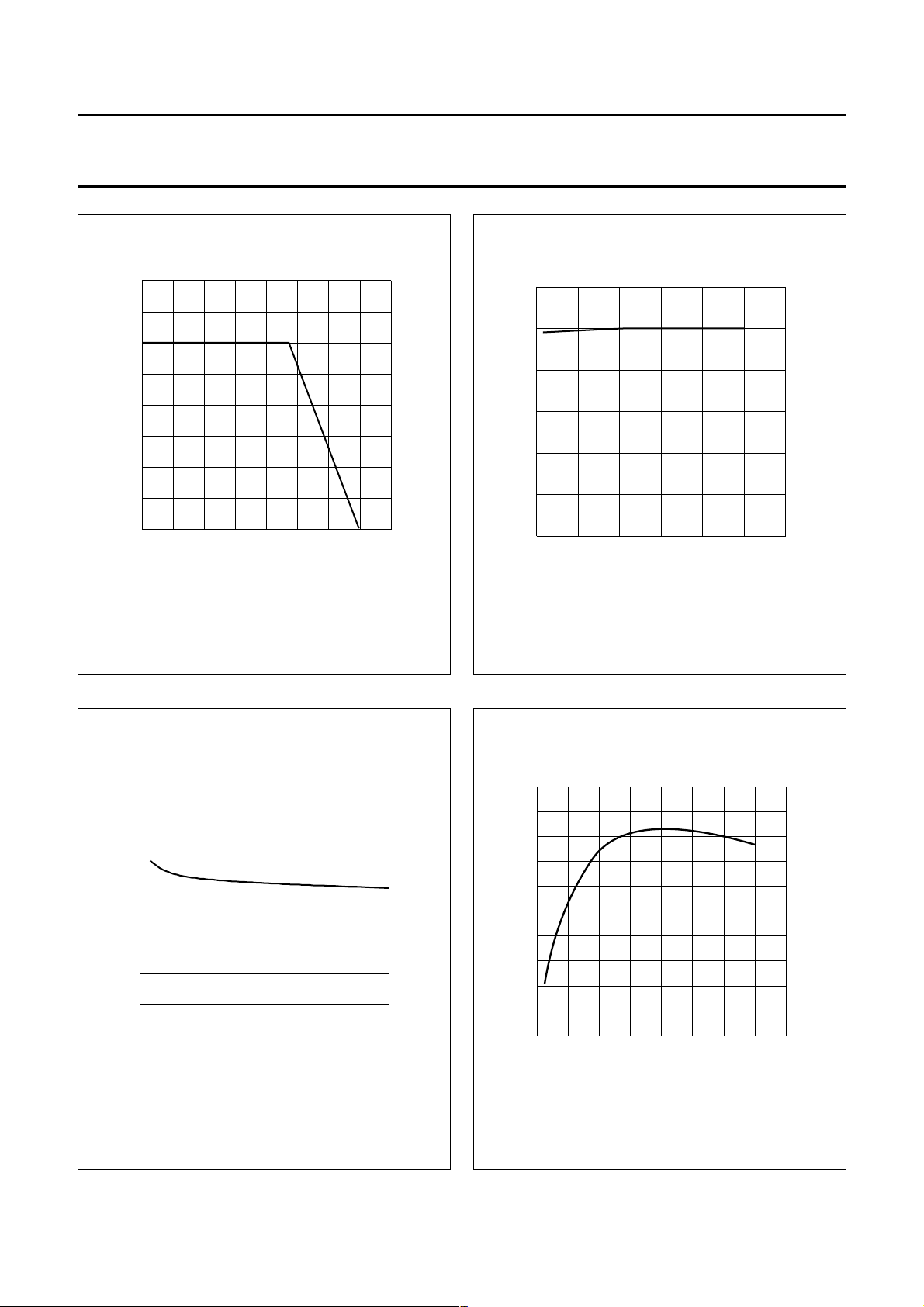
Fig.2 Power derating curve.
handbook, halfpage
0 50 100 200
400
300
100
0
200
MRC045- 1
150
P
tot
(mW)
Ts(
o
C)
Fig.4 Feedback capacitance as a function of
collector-base voltage.
IC=0; f=1 MHz.
handbook, halfpage
0
0.2
0.4
0.6
0.8
04812
MRC039
(pF)
V (V)
CB
C
re
NPN 8 GHz wideband transistor BFQ67T
120
handbook, halfpage
h
FE
80
40
0
0
VCE=5 V; Tj=25 °C.
20 40
MBB301
I (mA)
C
Fig.3 DC current gain as a function of collector
current.
60
30
MBB303
I (mA)
C
10
handbook, halfpage
f
T
(GHz)
8
6
4
2
0
01020 40
VCE= 8 V; f = 2 GHz; T
amb
= 25 °C.
Fig.5 Transition frequency as a function of
collector current.
1999 Oct 18 4
 Loading...