

DISCRETE SEMICONDUCTORS
DATA SH EET
BFQ621
NPN 7 GHz wideband transistor
Product specification
Supersedes data of 1995 Apr 11
File under Discrete Semiconductors, SC14
1995 Sep 26
Philips Semiconductors Product specification
NPN 7 GHz wideband transistor BFQ621
FEATURES
• High power gain
• High output voltage
• High maximum junction temperature
• Gold metallization ensures excellent reliability.
APPLICATIONS
It is primarily intended for use in MATV and microwave
amplifiers, such as aerial amplifiers, radar systems,
oscilloscopes, spectrum analyzers, etc.
PINNING
PIN DESCRIPTION
1 collector
2 emitter
3 base
4 emitter
QUICK REFERENCE DATA
DESCRIPTION
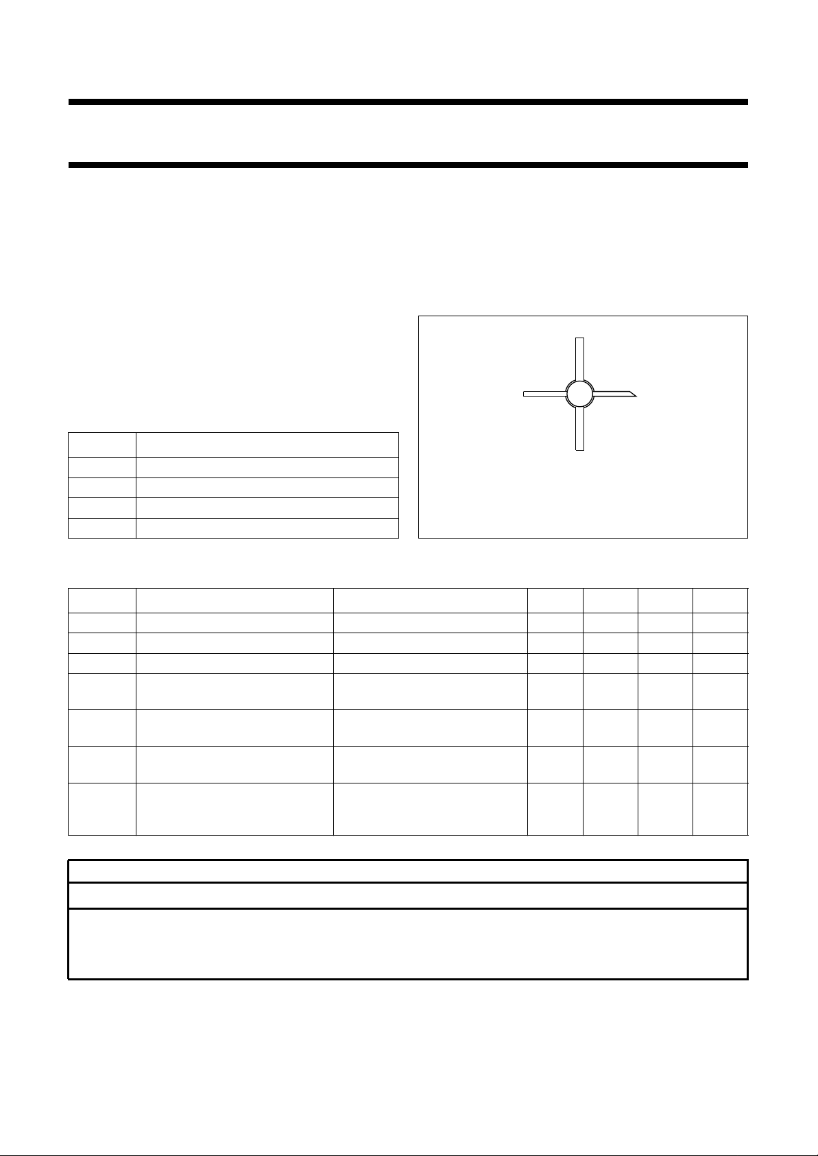
Silicon NPN transistor in a 4-lead dual-emitter SOT172A2
package with a ceramic cap. All leads are isolated from the
mounting base. Emitter ballasting resistors and application
of gold sandwich metallization ensures an optimum
temperature profile and excellent reliability properties.
handbook, halfpage
3
Top view
4
1
2
MSA457
Fig.1 SOT172A2.
SYMBOL PARAMETER CONDITIONS MIN. TYP. MAX. UNIT
V
CEO
I
C
P
tot
h
FE
f
T
G
UM
V
O
collector-emitter voltage open base −−16 V
collector current (DC) −−150 mA
total power dissipation up to Tmb=25°C −−8W
DC current gain IC= 120 mA; VCE=18V;
T
=25°C
amb
transition frequency IC= 120 mA; VCE=18V;
f = 1 GHz; T
amb
=25°C
maximum unilateral power gain IC= 120 mA; VCE=18V;
f = 500 MHz; T
amb
=25°C
output voltage IC= 120 mA; VCE=18V;
f
(p+q−r)
= 793.25 MHz;
40 −−
− 7 − GHz
− 18.5 − dB
− 1.2 − V
dim= −60 dB; RL=75Ω
WARNING
Product and environmental safety - toxic materials
This product contains beryllium oxide. The product is entirely safe provided that the BeO disc is not damaged.
All persons who handle, use or dispose of this product should be aware of its nature and of the necessary safety
precautions. After use, dispose of as chemical or special waste according to the regulations applying at the location of
the user. It must never be thrown out with the general or domestic waste.
1995 Sep 26 2
Philips Semiconductors Product specification
NPN 7 GHz wideband transistor BFQ621
LIMITING VALUES
In accordance with the Absolute Maximum Rating System (IEC 134).
SYMBOL PARAMETER CONDITIONS MIN. MAX. UNIT
V
CBO
V
CEO
V
EBO
I
C
P
tot
T
stg
T
j
THERMAL CHARACTERISTICS
SYMBOL PARAMETER CONDITIONS VALUE UNIT
R
th j-mb
collector-base voltage open emitter − 25 V
collector-emitter voltage open base − 16 V
emitter-base voltage open collector − 2V
collector current (DC) − 150 mA
total power dissipation up to Tmb=25°C − 8W
storage temperature −65 +175 °C
junction temperature − +200 °C
thermal resistance from junction to mounting base P
= 8 W; up to Tmb=25°C 21.9 K/W
tot
1995 Sep 26 3
 Loading...