

Philips BFQ540 Datasheet

DISCRETE SEMICONDUCTORS
DATA SH EET
ook, halfpage
M3D109
BFQ540
NPN wideband dual transistor
Product specification
Supersedes data of 1995 Sep 04
File under Discrete Semiconductors, SC14
1998 Aug 27
Philips Semiconductors Product specification
NPN wideband dual transistor BFQ540
FEATURES
• High gain
• High output voltage
DESCRIPTION
NPN wideband dual transistor in a
plastic SOT89 package.
age
• Low noise
• Gold metallization ensures
excellent reliability
• Low thermal resistance.
APPLICATIONS
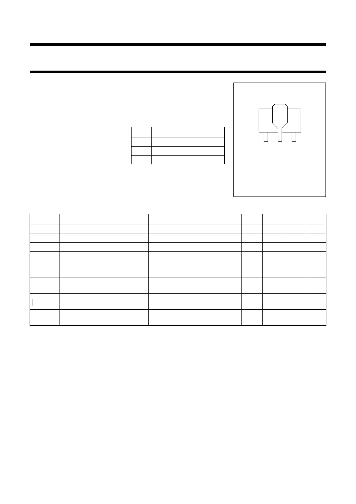
PINNING
PIN DESCRIPTION
1 emitter
2 collector
3 base
123
Bottom view
MBK514
• VHF, UHF and CATV amplifiers.
Marking code: N4.
Fig.1 SOT89.
QUICK REFERENCE DATA
SYMBOL PARAMETER CONDITIONS MIN. TYP. MAX. UNIT
V
CBO
V
CES
V
EBO
I
C
P
tot
h
FE
f
T
S
21
F noise figure I
collector-base voltage open emitter −−20 V
collector-emitter voltage RBE=0 −−15 V
collector-base voltage open collector −−2V
collector current (DC) −−120 mA
total power dissipation Ts≤ 60 °C; note 1 −−1.2 W
DC current gain IC= 40 mA; VCE=8V; Tj=25°C 60 120 250
transition frequency IC= 40 mA; VCE= 8 V; f = 1 GHz;
=25°C
T
amb
insertion power gain I
2
= 40 mA; VCE=8V;
C
f = 900 MHz; T
= 40 mA; VCE=8V;
C
amb
f = 900 MHz; ΓS= Γ
=25°C
opt
− 9 − GHz
12 13 − dB
− 1.9 2.4 dB
Note
1. T
is the temperature at the soldering point of the collector pin.
s
1998 Aug 27 2

Philips Semiconductors Product specification
NPN wideband dual transistor BFQ540
LIMITING VALUES
In accordance with the Absolute Maximum Rating System (IEC 134).
SYMBOL PARAMETER CONDITIONS MIN. MAX. UNIT
V
CBO
V
CES
V
EBO
I
C
P
tot
T
stg
T
j
THERMAL CHARACTERISTICS
SYMBOL PARAMETER CONDITIONS VALUE UNIT
R
th j-s
collector-base voltage open emitter − 20 V
collector-emitter voltage RBE=0 − 15 V
emitter-base voltage open collector − 2V
collector current (DC) − 120 mA
total power dissipation Ts≤ 60 °C − 1.2 W
storage temperature −65 +150 °C
operating junction temperature − 175 °C
thermal resistance from junction
Ts≤ 60 °C; P
= 1.2 W 95 K/W
tot
to soldering point
1.4
P
tot
(W)
1.2
1.0
0.8
0.6
0.4
0.2
0
0 50 100 200
VCE≤ 9V.
Fig.2 Power derating curve.
150
Tj (
MBG241
o
C)
3
10
handbook, halfpage
I
C
(mA)
2
10
10
1
10 10
Fig.3 SOAR.
VCE (V)
MBG244
2
1998 Aug 27 3
 Loading...