

Philips BFQ34-01 Datasheet

DATA SH EET
Product specification
File under Discrete Semiconductors, SC14
September 1995
DISCRETE SEMICONDUCTORS
BFQ34
NPN 4 GHz wideband transistor
September 1995 2
Philips Semiconductors Product specification
NPN 4 GHz wideband transistor BFQ34
DESCRIPTION
NPN transistor encapsulated in a 4
lead SOT122A envelope with a
ceramic cap. All leads are isolated
from the stud.
It is primarily intended for driver and
final stages in MATV system
amplifiers. It is also suitable for use in
low power band IV and V equipment.
Diffused emitter-ballasting resistors
and the application of gold sandwich
metallization ensure an optimum
temperature profile and excellent
reliability properties. The device also
features high output voltage
capabilities.
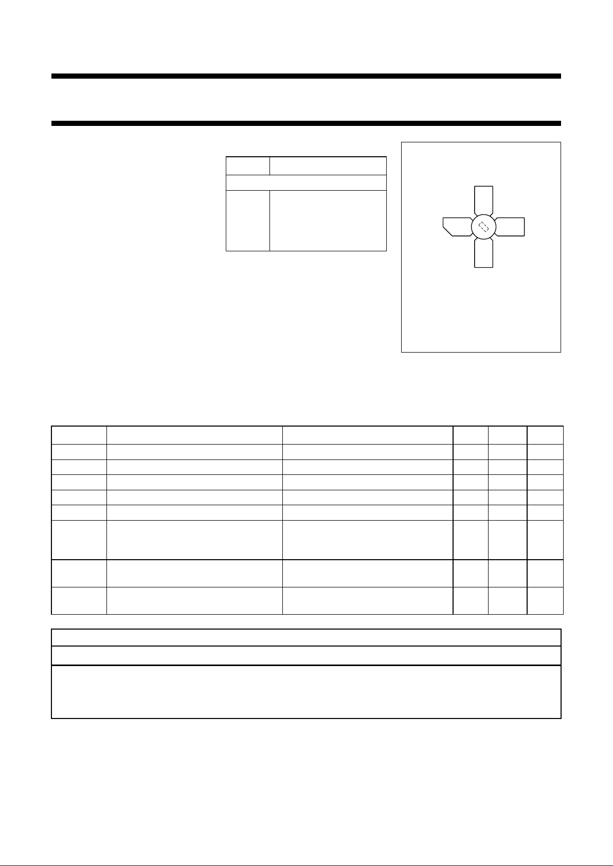
PINNING
PIN DESCRIPTION
Code: BFQ34/01
1 collector
2 emitter
3 base
4 emitter
Fig.1 SOT122A.
fpage
Top view
MBK187
31
2
4
QUICK REFERENCE DATA
SYMBOL PARAMETER CONDITIONS TYP. MAX. UNIT
V
CBO
collector-base voltage open emitter − 25 V
V
CEO
collector-emitter voltage open base − 18 V
I
C
collector current − 150 mA
P
tot
total power dissipation up to Tc = 160 °C − 2.7 W
f
T
transition frequency IC = 150 mA; VCE = 15 V; f = 500 MHz 4 − GHz
V
o
output voltage IC = 120 mA; VCE = 15 V; RL =75Ω;
T
amb
= 25 °C; dim= −60 dB
f
(p+q-r)
= 793.25 MHz
1.2 − V
P
L1
output power at 1 dB gain
compression
IC = 120 mA; VCE = 15 V; RL =75Ω;
f = 800 MHz; T
amb
= 25 °C
26 − dBm
ITO third order intercept point I
C
= 120 mA; VCE = 15 V; RL =75Ω;
T
amb
= 25 °C
45 − dBm
WARNING
Product and environmental safety - toxic materials
This product contains beryllium oxide. The product is entirely safe provided that the BeO disc is not damaged. All
persons who handle, use or dispose of this product should be aware of its nature and of the necessary safety
precautions. After use, dispose of as chemical or special waste according to the regulations applying at the location of
the user. It must never be thrown out with the general or domestic waste.
September 1995 3
Philips Semiconductors Product specification
NPN 4 GHz wideband transistor BFQ34
LIMITING VALUES
In accordance with the Absolute Maximum System (IEC 134).
THERMAL RESISTANCE
SYMBOL PARAMETER CONDITIONS MIN. MAX. UNIT
V
CBO
collector-base voltage open emitter − 25 V
V
CEO
collector-emitter voltage open base − 18 V
V
EBO
emitter-base voltage open collector − 2V
I
C
DC collector current − 150 mA
P
tot
total power dissipation up to Tc = 160 °C − 2.7 W
T
stg
storage temperature −65 150 °C
T
j
junction temperature − 200 °C
SYMBOL PARAMETER THERMAL RESISTANCE
R
th j-c
thermal resistance from junction to case 15 K/W
 Loading...