

Page 1

ChungHwa Picture tubes ,Ltd
OE Business Unit
P D P
Service Menu
Polished by After Service Section
APP Dept. Product Planning Division
First Edition Copyright : Ver_001.
All Rights Reversed
0
Page 2

Content :
0. Safety measures / Attention…………………….…………………………………
1. Summary …………………………………………………
2. Introduction to PDP circuit boards………………….……………………………
2.1 VIF board ………………………………………………………………………
2.1.1 VIF basic framework………………………………………………………
2.1.2 Photos of VIF Board……………………………………………………….
2.1.3 Pin assignments of connectors ……………………………………………..
2.1.4 VIF (Video interface)……………………………………………………….
2.1.5 System Block diagram………………………………………………………
2.1.6 Some Waveforms…………………………………………………………….
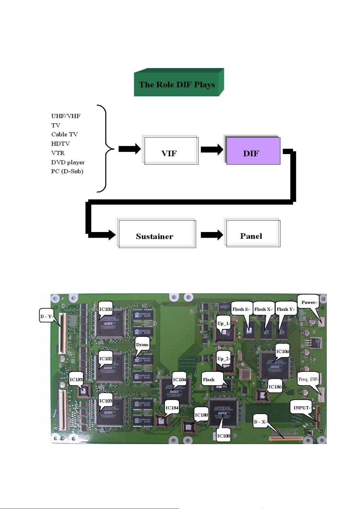
2.2 DIF board ………………………………………………………………………
2.2.1 DIF 2.95 board……………………………………..………………………
2.2.2 Equipments…………………………………………………………………
2.2.3 Simple electric circuit test………………………….………………………
2.2.4 Advanced electric circuit test………………………………………………
2.2.5 IC100 - IC106 :main signal waveform measuring….………………………
2.2.6 Waveform …………………………………………………………………
2.3 POWER board …………………………………………………………………
2.3.1 Introduction ………………………………………….……………………
2.3.2 The output power………………………………………..…………………
2.3.3 pin assignments of connectors…………………………………………….
2.3.4. Troubleshooting…………………………………………………………..
2.4 X-Sustainer board ………………………………………………..……………
2.4.1 X-Sustainer board’s pin alignments ………………………………………
2.4.2 X-side function explanation :………………………………………………
2.5 Y-Sustainer board ………………………………………………………………
2.5.1 Y-Sustainer board’s pin alignments…………………………………………
2.5.2 Y-side function explanation…………………………………………………
3. PDP repairing flow-chart …………………………………………………………
3.1 Main flow-chart………………………………………………………………
3.2 No picture repairing flow-chart………………………………………………
3.3 X sustainer malfunction repairing flow-chart…………………………………
3.4 Y sustainer malfunction repairing flow-chart…………………………………
4. Generally common defective checking and testing…………………………………
4.1 Phenomenon 1 : Dark screen and flickering…………………………………..
4.2 Phenomenon 2 : 170v limit current……………………………………………
1
Page 3

4.3 Some phenomenon of failure PCB boards……………………………………..
5. Debug / Inspection…………………………………………………………………….
5.1 Debug………………………………………………………………………….
5.2 Inspection………………………………………………………………………
6. Common use of BOM lists …………………………………………………………
7. Repair record: …………………………………………………………………………
2
Page 4

0. Safety measures and Attentions:
1. Observation and measures carefully:
When in repair service , should pay attention to these safety measures and the description
Of the service menu.。
2.Preparation:
The preparation for repair in a defective PDP is necessary , ex:stable working table , repair
Tools , measuring equipments , replace parts………etc。
3.Pay attention to electrical shock:
Because the PDP is using the AC power source , and the power board contents high voltage ,
so to preventing the high voltage shock is necessary . Such as , using a isolated transformer ,
plastic glove , charged components should be discharged first . The high voltage is supplied
to inferior components , so when repair the PDP should pay more attentions.
4.Using the specified components:
Some components provide fire-resist and endure high-voltage. So when replace these parts
, should use the same characteristic components. So when replace a component should according
to the BOM form for a assigned component.
5.Stable the components and recovery the wiring :
Some components are using isolated sleeve or adhesive tape to isolate from the electric
board . Moreover the interior wiring should be arranged again to prevent the interference
from given out heat components and high voltage components .So after repairing , should
recover the same layout of the PDP.
6.Integrity of the electric circuit :
Use the specified components to replace the defective parts . Under any circumstance,do
not try to modified the electric circuit .
7.Safety check after repairing:
After repairing , should check the screws and the wiring condition .Checking the quality
of repairing components . The insulation test of the metal component , power cord to make
sure the safety of repairing.
3
Page 5
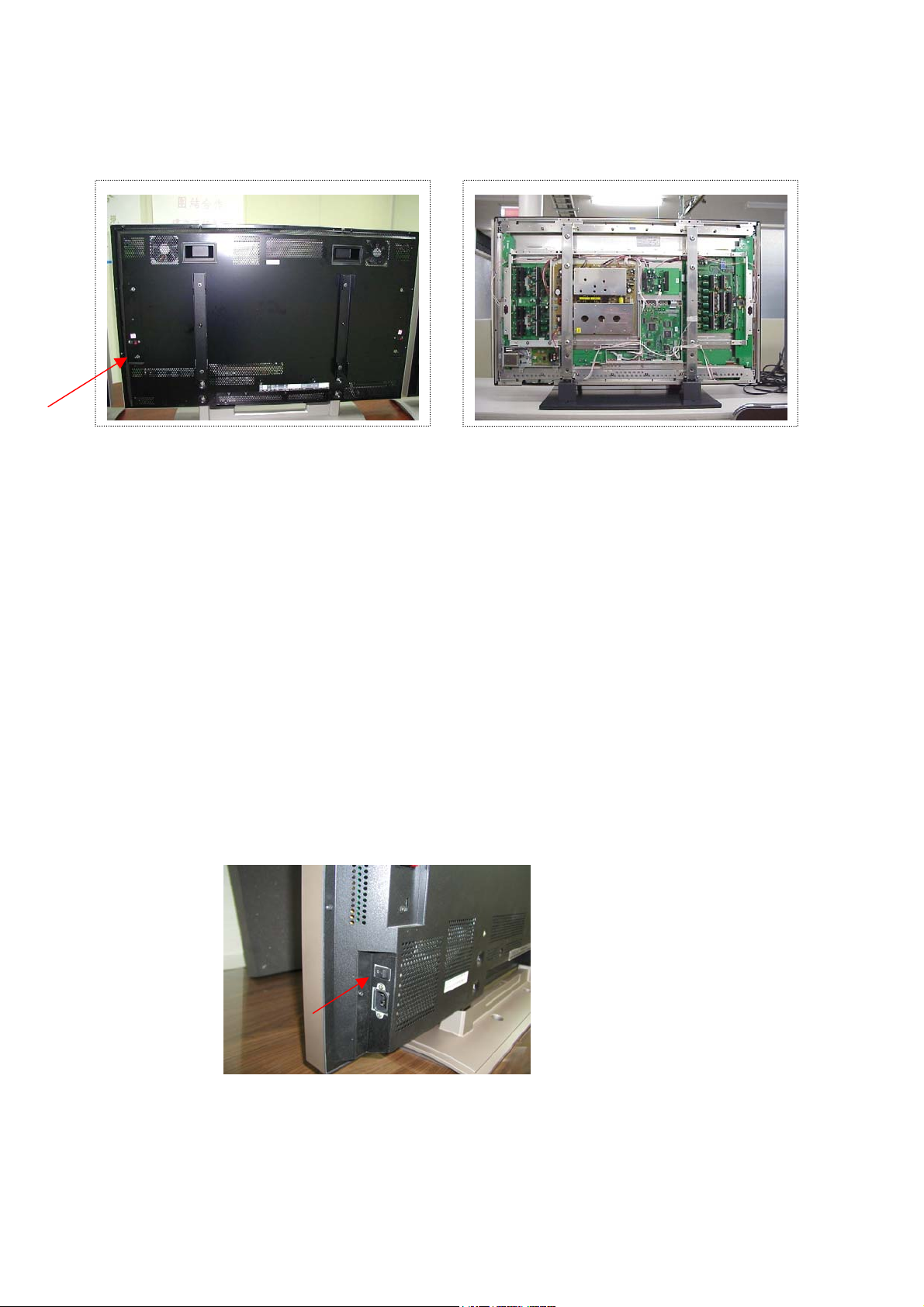
1 . Summary :
N
1.1 Photos of disassembly:
ote.3
Fig. 1 Fig. 2
1.2 Procedure:
1.First put on the PDP on a stable working table and power off the PDP which is going to repair ,
then using a screwdriver to unfasten the screws which fasten the back cover .
2.Befor taking apart as Fig.1 shown , after taking apart as Fig. 2 shown .
3.The screws of back cover:
a. pan-headed screw M4 *13 pcs。
b. screw TB-12 *18 pcs。
c. stand screw M5-16 * 4pcs。
1.3 Note:
2.After taking apart , put the screws at a safe place to avoid losing
1.Make sure that the power is off before taking apart .
3.Taking apart and installing the back cover , be careful not to pull out the switch of AC power
switch .(Fig.3)
Fig.3
4
Page 6
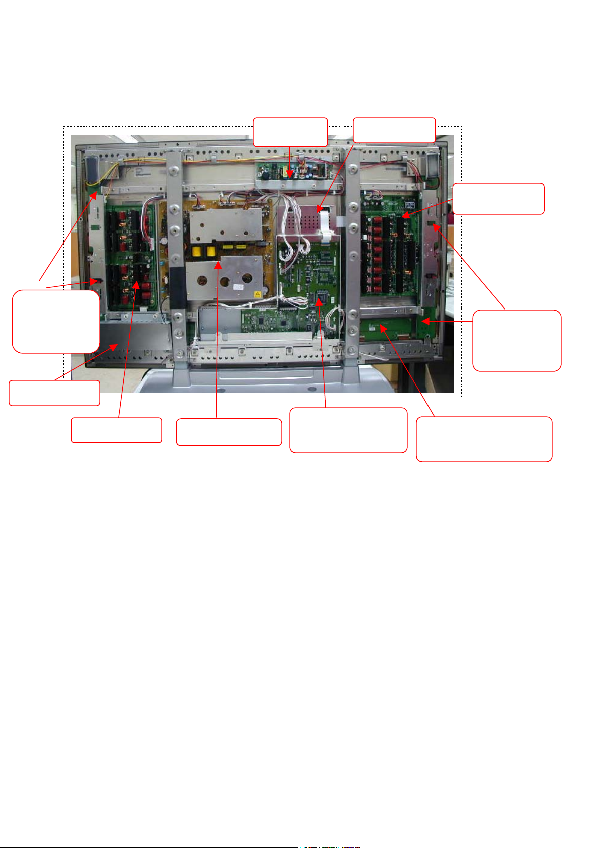
1.4 Introduction to PDP circuit board:
d
)
)
1.4.1The introduction of circuit board at Back board:
Y-Extension
board (upper
and lower
AC Line Filter
Y-SUSTAINER
1.4.2 Explanation:(Function / Characteristic)
POWER SUPPLY
Audio Board
VIF(PC Module &
Video Module)
DIF Boar
X-SUSTAINER
X-Extension
board (upper
and lower
W-Extension board (left
and right)
a. POWER:(1).Input Voltage (AC 110V〜240V、47HZ〜63HZ),Max. range 90V〜265V.
(2).Providing electrical power to all the PCB.
b. VIF:Transfer S-video , Video , PC(D-sub& DVI) , HDTV signal to digital signal to the DIF
board.
c. DIF:Dealing with the digital signal for output to panel.
d. X-Sustainer / Y-Sustainer:(1).Receiving the signal from DIF.
(2). Output scanning waveform.
e. X / Y-Extension board: Receive signal from X / Y sustainer , output horizontal scanning waveform
to the panel.
f. W-Extension board: Receive signal from DIF , output the vertical scanning waveform , addressing
data.
g. Audio Board:Amplifying the audio signal to the internal or external speakers of which select.
h. AC Line Filter:AC power line filter。
5
Page 7
1.4.3. PDP 46” block diagram:
pp
W
d
W
Y
Lower
Uppe
Y-
PY
r
Y- S us t ai n er
-
PY PX1 PX2 PW
Key PAD
AC Filter
AC 90~240 V
Panel
POWER
-Board
Audio-AMP
J17
J12
Power CN1
J15 J16 CV1
DIF
V I F
DW1 DW2
J11
DW1 DW2
DX1
-Boar
PX1 PX2
DX1
X-Sustainer
X-U
er
X-Lower
Front Receiver
1.4.4 Function:
a. The input voltage AC 90 ~ 240 through line filter to the power board , after main switch is on
then power board generate 5 volts to VIF board. The VIF board after receiving 5 volts then
from CN connector send signal(5 volts) to power board .Power board generates 5 volts to DIF
and VIF .When VIF receives the 5 volts ,then generates 5 volts to power board through CN
connector(pin1 ,pin6) , and it means that DIF has received 5 volts already.
b. When power on(key-pad or receiver),the VIF send VCC_ON signal to power to start Vcc and
Vf voltage through CN connector(pin2).
c. The VIF sends HV_ON signal to power board to start high voltage Vs , Vxg , Vw through CN
connector(pin4).
d. At the same time the signal from VIF to DIF for signal processing , then through X / Y / W
board to start the screen.
6
Page 8
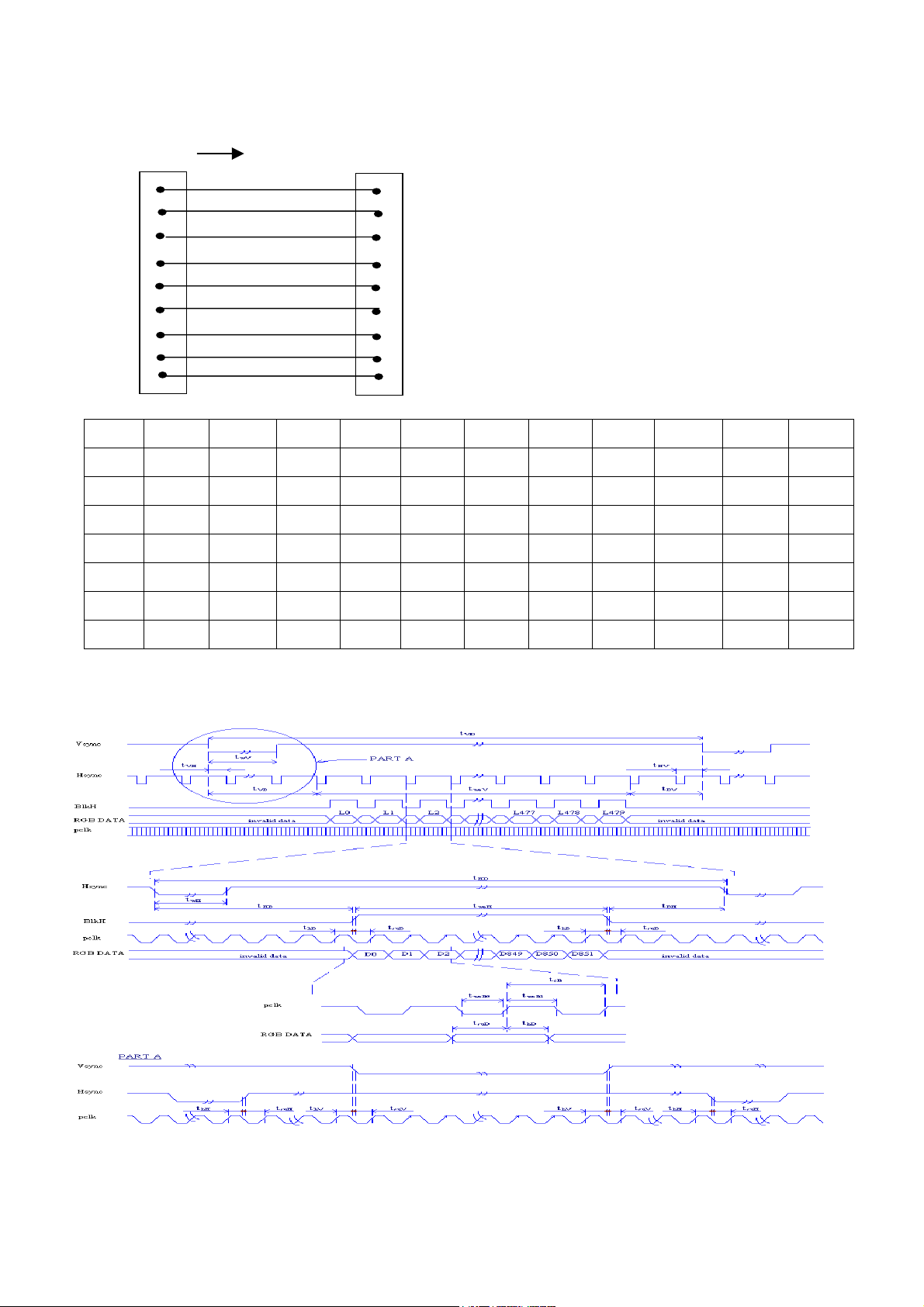
1.4.5 The waveform of connector:
a. CN1-V CN1-D:
8bit R [7:0]
8bit G [7:0]
8bit B [7:0]
clock
Hsync
Vsync
Blank (Blank H)
I*2C
a-1. PIN assignment :
PIN No.
Output
1 2 3 4 5 6 7 8 9 10 11
CLK0 CKL1 Gnd BLK Gnd VD Gnd HD Gnd Gnd B7
12 13 14 15 16 17 18 19 20 21 22 23
B6 B5 B4 Gnd B3 B2 B1 B0 Gnd G7 G6 G5
24 25 26 27 28 29 30 31 32 33 34 35
G4 Gnd G3 G2 G1 G0 Gnd R7 R6 R5 R4 Gnd
36 37 38 39 40 41 42 43 44 45
R3 R2 R1 R0 Gnd None TP66 none
Sda/TP5 Scl/TP2
a-2. Signal explanation:
7
Page 9
b. DX1 to DXS:
b-1 PIN assignment :
PIN No.
Output
1 2 3 4 5 6 7 8 9 10
Gnd
XDD2/TP1
40
XDD1/TP1
39
Gnd
XP2L/TP1
38
XG2L/TP1
37
XG3L/TP1
36
XG1L/TP1
35
Gnd
XG1H/TP
134
11 12 13 14 15 16 17 18 19 20 21
XSU/TP133 XAEL/TP1
52
XEAH/TP
151
Gnd
XELL/TB1
50
XEFH/TP1
49
Gnd
XNEL/TP1
48
XNEH/TP
147
Gnd
XCLK/TP1
46
22 23 24 25 26 27 28 29 30
Gnd
XSI2/TP14
5
Gnd
XLE/TB144 XSTB/TP1
42
XTSC/TP1
41
Gnd
XSI1/TP14
3
Gnd
c. DW1 to DW1(DIF to W board)
Signal:DDR(27.0)、DDG(27.0)、DDB(27.0)、DLE(2.0)、DBL(2.0)、DBH(2.0)、DHZ(2.0)。
PIN No.
Output
1 2 3 4 5 6 7 8 9 10 11
GED YSC2A YSC1A GED YEELA YEEHA GED YEFLA YEFHA GED YCA2B
12 13 14 15 16 17 18 19 20 21 22 23
YSC1B GED YNELB YNEHB GED YEFLB YEFHB GED DDB27 DDG27 DDR27 GED
24 25 26 27 28 29 30 31 32 33 34 35
DDB26 DDG26 DDR26 GED DDB25 DDG25 DDR25 GED DDB24 DDG24 DDR24 GED
36 37 38 39 40 41 42 43 44 45 46 47
DDB23 DDG23 DDR23 GED DDB22 DDG22 DDR22 GED DDB21 DDG21 DDR21 GED
48 49 50 51 52 53 54 55 56 57 58 59
DDB20 DDG20 DDR20 GED DDB19 DDG19 DDR19 GED DDB18 DDG18 DDR18 GED
60 61 62 63 64 65 66 67 68 69 70 71
DDB17 DDG17 DDR17 GED DDB16 DDG16 DDR16 GED DHZ2 DBH2 DBL2 DLE2
72 73 74 75 76 77 78 79 80
GED RAKa GED RAKb GED V50 V50 V50 V50
d. DW2 to DW2 (DIF to W board)
signal:DDR(27.0)、DDG(27.0)、DDB(27.0)、DLE(2.0)、DBL(2.0)、DBH(2.0)、DHZ(2.0)。
PIN N.
Output
1 2 3 4 5 6 7 8 9 10 11
V50 V50 V50 GED DDB15 DDG15 DDR15 DDB14 GED DDG14 DDR14
12 13 14 15 16 17 18 19 20 21 22 23
DDB13 DDG13 GED DDR13 DDB12 DDG12 DDR12 GED DDB11 DDG11 DDR11 DDB10
24 25 26 27 28 29 30 31 32 33 34 35
8
Page 10

GED DDG10 DDR10 DDB9 DDG9 GED DDR9 DDB8 DDG8 DDR8 GED DHZ1
36 37 38 39 40 41 42 43 44 45 46 47
DBH1 GED DBL1 DLE1 GED GAKa GED DHZ0 DBH0 GED DBL0 DLE0
48 49 50 51 52 53 54 55 56 57 58 59
GED GAKb GED DDB7 DDG7 DDR7 DDB6 GED DDG6 DDR6 DDB5 DDG5
60 61 62 63 64 65 66 67 68 69 70 71
GED DDR5 DDB4 DDG4 DDR4 GED DDB3 DDG3 DDR3 DDB2 GED DDG2
72 73 74 75 76 77 78 79 80
DDR2 DDB1 DDG1 GED DDR1 DDB0 DDG0 DDR0 GED
e. W-COF to Y-Sustainer:
PIN No
Output
PIN No
Output
1 2 3 4 5 6 7 8 9 10
LGED YSC2A YSC1A LGND YNELA YNEHA LGND YEFLA YEFHA LGND
11 12 13 14 15 16 17 18 19 20
LGND YSC2B YSC1B LGND YNELA YNEHA LGND YEFLB YEFHB LGND
9
Page 11

3
4.
1
3.
3
8.
1
3.
6
21.
0
1.
5
4.
4.5
6
0.
5
4.
0.6
5
4.
I,1 I,2 ............... I,484
Xv
X484
圖 4. 2
X1 X2 ...................
g
W
Y
Ya
Yb
XVDD
LOG2
XSI1
XLE
XSI2
XCLK
XTSC
XSTB
10
Page 12
3
4.
1
3.
3
8.
1
3.
6
21.
0
1.
4.5
4.5
0.6
4.5
0.6
4.5
X484
X1 X2 ...................
I,1 I,2 ............... I,484
g
Xv
W
Y
*
Yb
Ya
XLFH
XEFL
XNEL
XG1H
XNEH
XG1L*
XG2L
*
XP2L
*
XS
H
U
XAE
XAEL
XDD1
XDD2*
XTSC
圖 4. 1
XSTB
11
Page 13
12
Page 14
f. Power signal:Power to Y-Sustainer (PY):
PIN No.
Symbol Vcc-G Vcc Vf-G Vf Vw Vw-G Vs-G None Vs
Output 5V 5V 15v 15v 65V 65V 170V None 170v
g. Power signal : Power to X-Sustainer (PX1):
PIN No. 1 2 3 4 5 6 7
Symbol Vf-G Vf Vw Vw-G Vs-G None Vs
Output 15v 15v 65V 65V 170V None 170v
h. Power signal:Power to X-Sustainer (PX2):
PIN No. 1 2 3 4 5
Symbol Vxg None Vxg-G Vcc Vcc
Output -160V None 15v 15v 65V
1 2 3 4 5 6 7 8 9
2.1 VIF Board:
Summary:
General digital video signals include Vsync、Hsync、R(8Bit)、G(8Bit)、B(8Bit) and Data
Enable(Blank);the VIF of PDP is making for processing these digital signal.
Because PDP belonging a high end product , so its application should include the functions of
monitor(analog VGA , digital DVI signal input). And for consumer’s sake , the VIF should have the
functions of video , like audio , composite , s-video , component signal processing.
Below is the explanation of VIF system:
The role of VIF:
UHF/VHF TV
Cable TV
HDTV
VTR
DVD Player
PC
Home Video Game
DIFVIF
13
Page 15
Currently the video signal sources are video cassette recorder , DVD player , CATV , RF tuner , VGA
card(PC). In order that all the video signal sources can be displayed on PDP , so we need a interface to
transfer these signals to a specified signals for PDP to display , and this is the function of VIF(Video
Interface).
2.1.1 Basic framework of VIF board
For dealing with the signals of CVBS , S-video and Component, it requires a video decoder IC .
And the output of video decoder will input to a de-interlace chip IC for a stable image quality .
Because the TV system uses interlace scanning , it causes flickers on the screen . To improve this
situation so we use a de-interlace chip IC . The ADC(Analog to Digital Converter) IC converts
the analog RGB signal to digital RGB signal. The TMDS(
decoder IC transmits digital RGB signal. All the output of ICs’ signal send to scalar IC. The
relationship is shown as below , and make a brief explanation of the system.
Transition Minimized Differential Signaling)
D-SUB
ADC
Converter
Scalar
Chip
Out to DIF
DVI
TMDS
Receiver
Y/Cb/Cr
De_
Interlace
S-Video
Composite
Video
Decoder
Micro_
Controller
a. ADC Converter:AD9888 KS
RGB graphics signals. Its 205 MSPS encode rate capability and full-power analog bandwidth of
500 MHz supports resolutions up to UXGA(1600 x1200 @ 75 Hz).
The AD9888 is a complete 8 bit , 205 MSPS monolithic analog interface optimized for capturing
b. TMDS Receiver: SIL153BCT100
The Sil153BCT100 receiver uses PanelLink Digital technology to support high resolution displays up
to SXGA(25MHz~112MHz) . The Sil153B receiver supports up to true color panels (24 bit/pixel,
16.7M colors) in 1 or 2 pixels/clock mode. In addition , the receiver data output is time staggered to
14
Page 16
reduce ground bounce that affects EMI.
c. VIDEO Decoder:SAA7118E
The SAA7118E decoder is a ADC too , but it can deal with the ordinary TV signals. The
SAA7118E can input Composite (fig.A)、S-video (fig.B)、Component (fig.C) and its outputs
Are digital Y(Luminance) , C(Chromacity) signals. And also can adjust brightness , contrast ,
Saturation , hue .
Fig.A : Composite 信號 for COLOR BAR
Fig.B-1 YY ssiiggnnaall ooff SS--vviiddeeoo
15
Page 17
g
g
g
g
d
d
i
FFi
..BB--22CCssi
i
nnaallooffSS--vvi
i
o
eeo
FFiigg..CC--11 YY--ssiiggnnaall ooff CCoommppoonneenntt
FFiigg..CC--22 CCbb--ssiiggnnaall ooff CCoommppoonneenntt
16
Page 18
d. De-interlace:SIL504CM208
FFiigg..CC--33 CCrr--ssiiggnnaall ooff CCoommppoonneenntt
The Sil504 transfer interlacing signals to progressive signals. The advantage of progressive
signals is that the scanning rate doubling to let the screen more stable and non-flickering. Besides, the
sources of input may have 24 0r 30 or 25 frames per sec, so the de-interlaced chip shall tell from the
differences and processing the signals. The basic principle of de-interlaced IC is combined the odd and
even fields to a frame , and the processing needs a memory IC(SDRAM) to store these signals for
processing . For the improving the quality of image sake , more and more TVs or DVD players all
have the functions of progressive scanning.
e. Image Processor chip:PW171-20U(system on chip)
◎ Scaling function :
The Image scalars provide high quality up and down image scaling . For the applications of VIF , the
input signals could be VGA , SVGA , XGA formats , and its output fixed at 852 x 480 @60 HZ . For
example , SVGA format:800 x 600 @75Hz , first scaling down : Horizontal 800Î640、Vertical
600Î480 , 75 frames / sec after frame rate conversion become 60 frames per sec. Then scaling up
640Î852 , to accomplish the scaling function.
◎ Micro Processor Function :
This chip includes microprocessor(on-chip 80x86) ; selectable function and I/O interface control .
With 3 groups of 8-bit programmable I/O , 1 group of RS-232 communication port , IR
decoder ,timer and a PWM generator
17
Page 19
◎ OSD Function :
3
o/Video
S-VideoY/Cb/Cr
Video Decoder
Switc
V
The on-screen-display(OSD) can be used for startup screens , menus , and scribble functions.
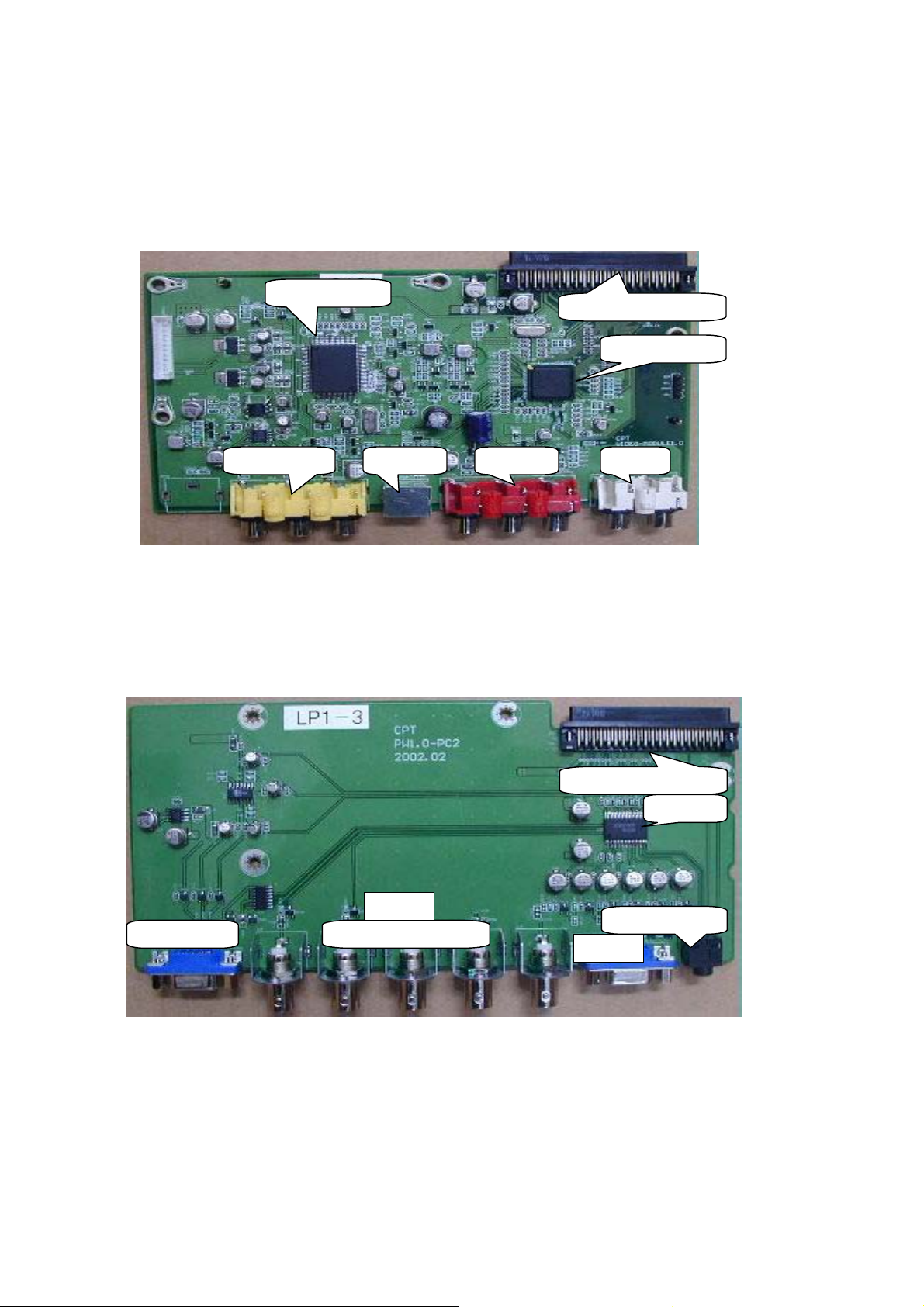
2.1.2 Photos of VIF Board :
a. Video Module:
Audi
b 2nd PC Module:
D Y/C SEP
To VIF Main Board
Audio
To VIF Main Board
h
PC OUT
H B G R
PC Audio IN
18
Page 20
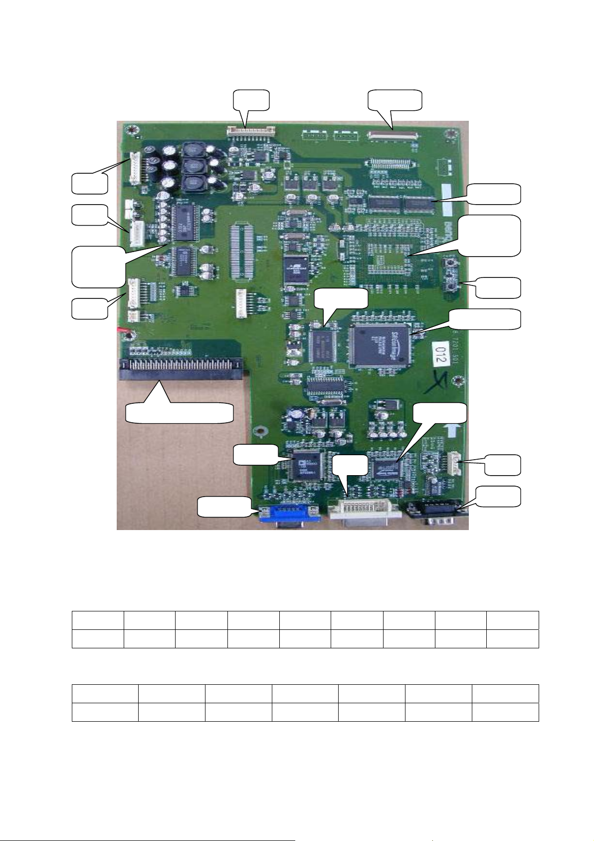
c. VIF Main Board:
J16
To DIF
J15
SDRAM
J17
Image
Processor
Tone
Control
Reset
SDRAM
J12
De_interlace
To Video/PC Module TMDS
ADC
D-SUB
DVI
2.1.3 Pin assignments of connectors :
a. J12 : Key Pad Signal
NO
ITEM Power Right Left Up Down Menu Input Gnd
b. J11 : Receiver/Indicator Signal
1 2 3 4 5 6 7 8
J11
RS232
NO
ITEM NC Red LED Green LED Gnd Ir_Rcv +5V
1 2 3 4 5 6
19
Page 21
c. J17 : Audio Signal
NO 1 2 3 4 5 6
ITEM Mute L_Out L_Gnd R_Out R_Gnd
SPK
Int/Ext
d. J16 : Power –Control Signal
NO 1 2 3 4 5 6 7 8 9 10
+5V
ITEM
LV ON NC HV ON NC Gnd Fault Pwloss Fan Gnd
Standby
e. J15 : Power –Supply Voltage
NO 1 2 3 4 5 6 7 8 9
ITEM
+9V
Audio
+9V
Audio
GND GND
+5V
VCC
+5V
GND GND
VCC
f. J9:Output – Out to DIF
1/
SCL
2/
SDA
3/
NC
4/
NC
5/
Status
6/
GND
7/
R-00
8/
R-01
+5V
Standby
9/
R-02
10/
R-03
19/
G-02
28/
B-01
37/
GND
11/
GND
20/
G-03
29/
B-02
38/
H-sync
12/
R-04
21/
GND
30/
B-03
39/
GND
13/
R-05
22/
G-04
31/
GND
40/
V-sync
14/
R-06
23/
G-05
32/
B-04
41/
GND
15/
R-07
24/
G-06
33/
B-05
42/
Blanking
16/
GND
25/
G-07
34/
B-06
43/
GND
17/
G-00
26/
GND
35/
B-07
44/
PixelCLK
18/
G-01
27/
B-00
36/
GND
45/
GND
2.1.4 VIF (Video interface) :
a. When main switch is ON , the power board generates Vsby 5 volts to VIF board. The IC of
microprocessor become standby status waiting for a startup signal from key-pad or receiver.
b. When a startup signal is detected then microprocessor sending a ON signal to the power board
through CN connector , and the power board begins generating all voltage to PCB board(Vs ,
Vxg , Vw , Vf , Vdd , Vcc , 9volts) . At the same time VIF will generate background light and
OSD menu as select .After searching a input source , then will display on the PDP screen , if
there are audio signals , it will amplify and send to speakers through audio board.
c. If there are abnormal signals are detected(such as over voltage , over current , low voltage ..) , the
power board will send abnormal detective signal to shut down all the system.
20
Page 22
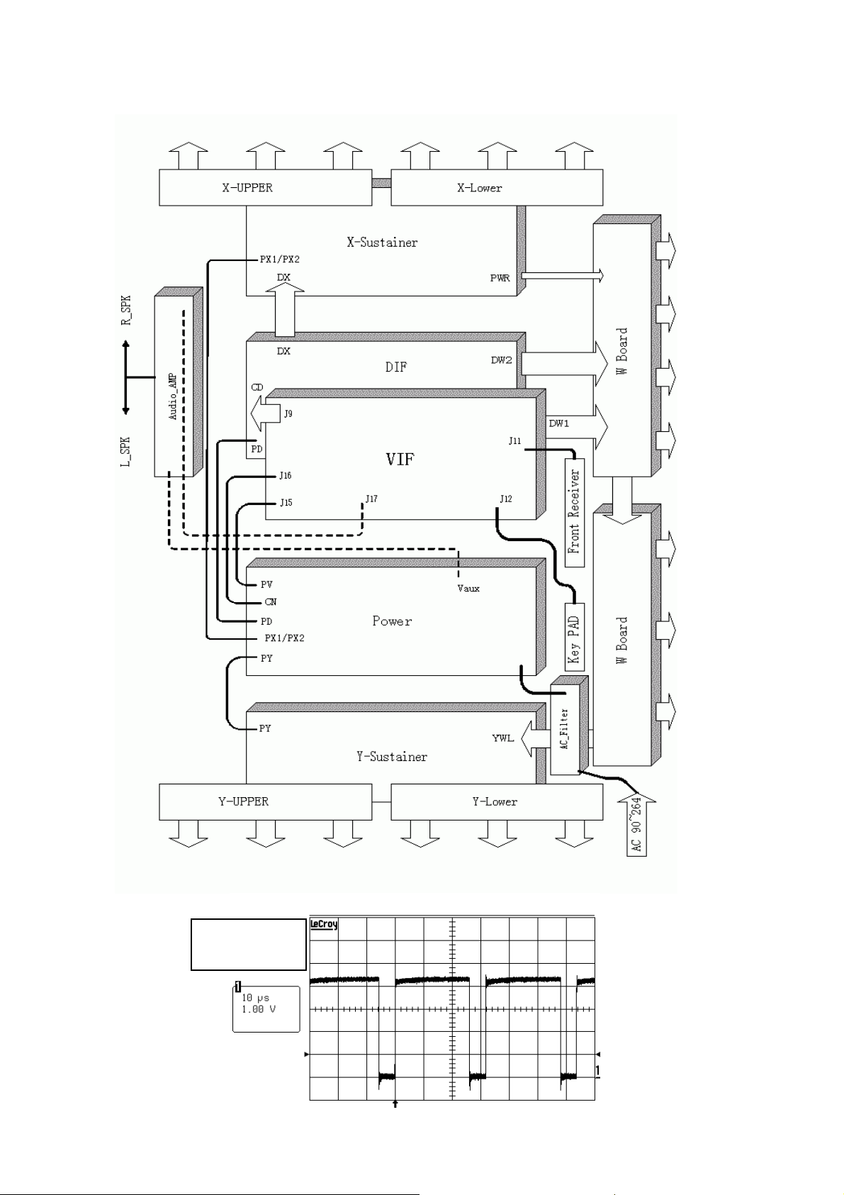
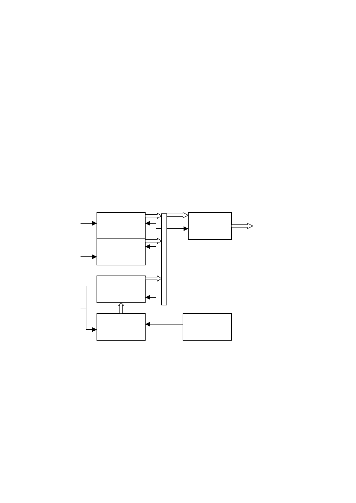
2.1.5 System Block diagram :
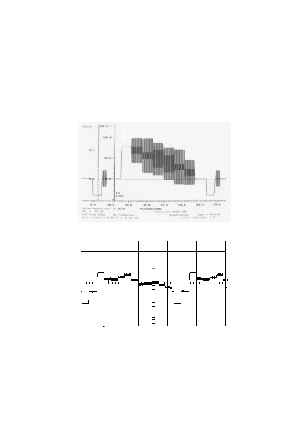
2.1.6 Some Waveforms:
J9_42 TP155
Blanking
21
Page 23
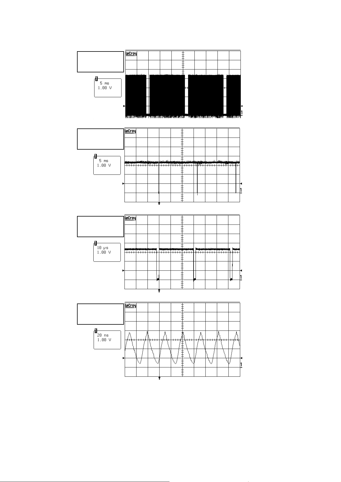
J9_42 TP155
Blanking
J9_40 TP154
Vsync
J9_38 TP152
Hsync
J9_44 TP156
PixelClock
22
Page 24
2.2. DIF board:
2.2.1 DIF 2.95 board:
DIF 2.95 board :
Fig. 1 The role of DIF board
Fig.2 The photo of a DIF board
23
Page 25
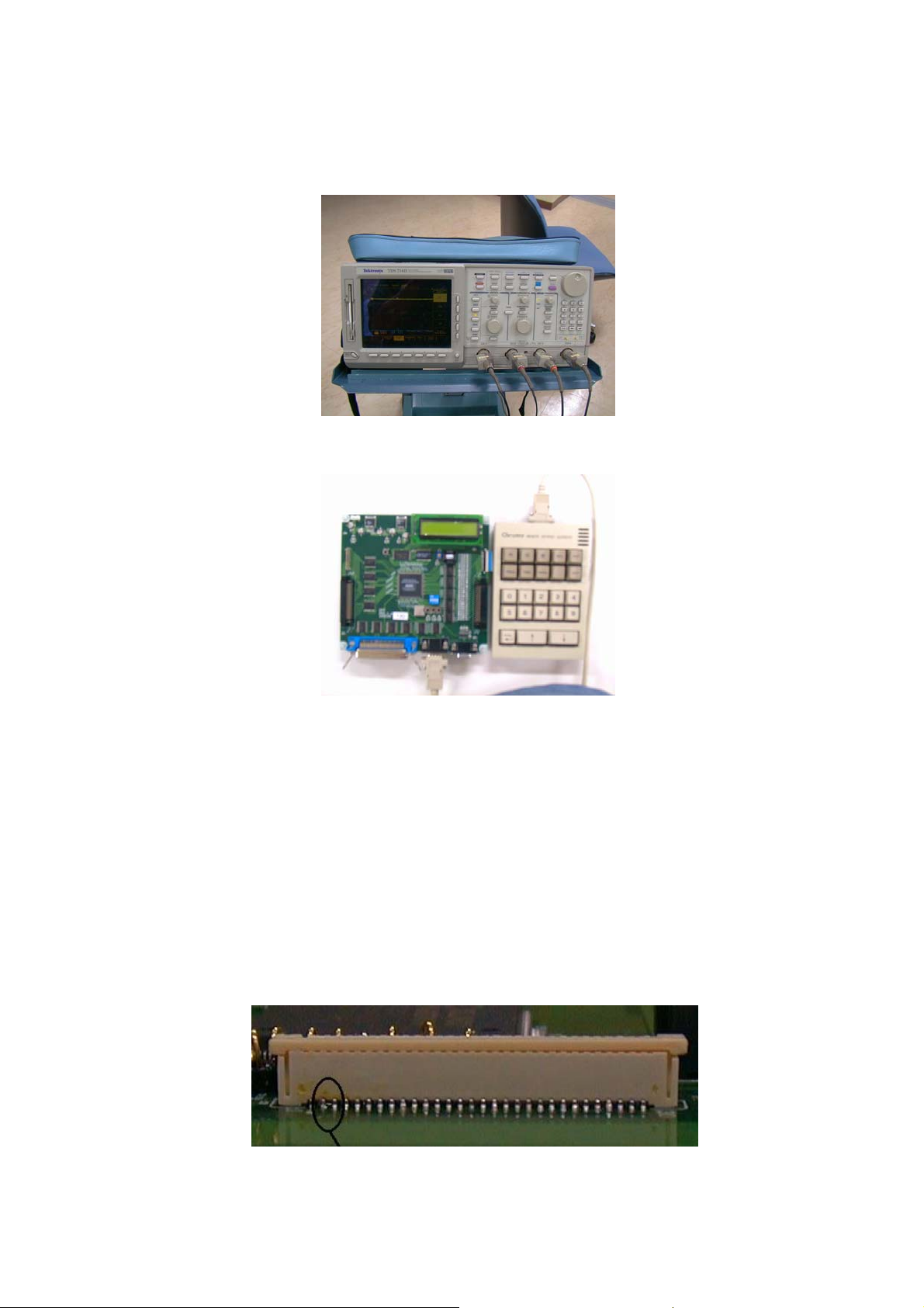
2.2.2 Equipments:
a. Power : 5V 3A power supply * 1
b Tools:
b-1 Oscilloscope
b-2 PMC
Fig. 3 Oscilloscope with 4 channels
b-3 45 pin FFC connector * 1
b-4 Multi-meter * 1
c. Test flow
c-1 Overall check:
To inspect the DIF board whether broken board occurred , components broken or short
circuit…. etc .
Ex:
(1)
Fig.4 PMC * 1
Fig. 5 Connector short circuit
24
Page 26
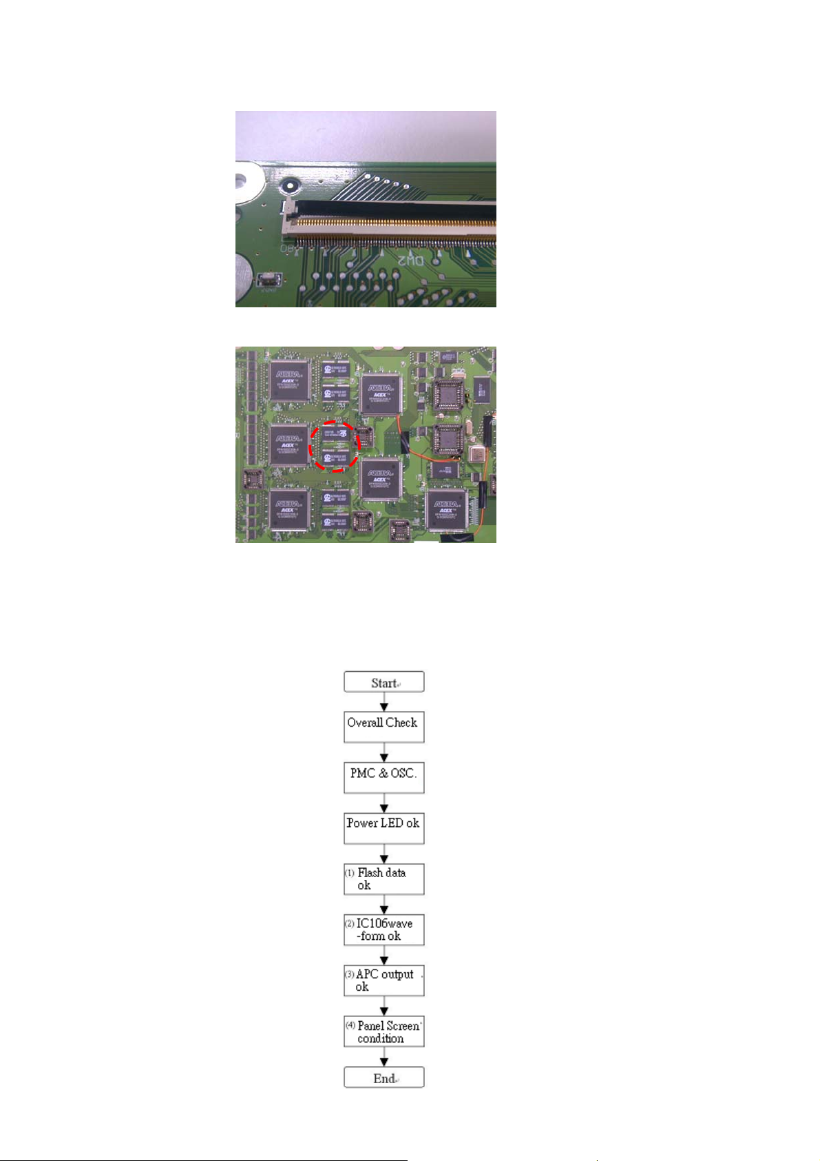
(2)
Fig.5 D to W connector broken
(3)
c-2 Power test:
Make sure that the power is normal without any short circuit happening.
2.2.3 Simple electric circuit test:
Checking all functions of the board is normal.
Test flow as Fig.7 shown.
Fig.6 Wrong DRAM
Fig.7 Test flow
25
Page 27
** LED : When DIF power on , the LED light on means that the FPGA download OK , at this time the
p
current will be about 1.3A .
a. Waveform testing :
a-1 Make sure that the waveforms of S , X , Y are normal . Repeat reading the data from IC to
make sure the downloading data is normal.
a-2 The Waveform of IC106 : If the waveforms of S , X , Y are normal. Then we can check
the functions of controlling waveforms of IC106.
a-3 Next procedure is going to check the waveform of V、Start、Wp、Wn、SF0~SF3、Esq.
Check Vf , Vf is signal after processing from V. SF0~SF3 , Esq is the setting time and
ending time of the sub-field .
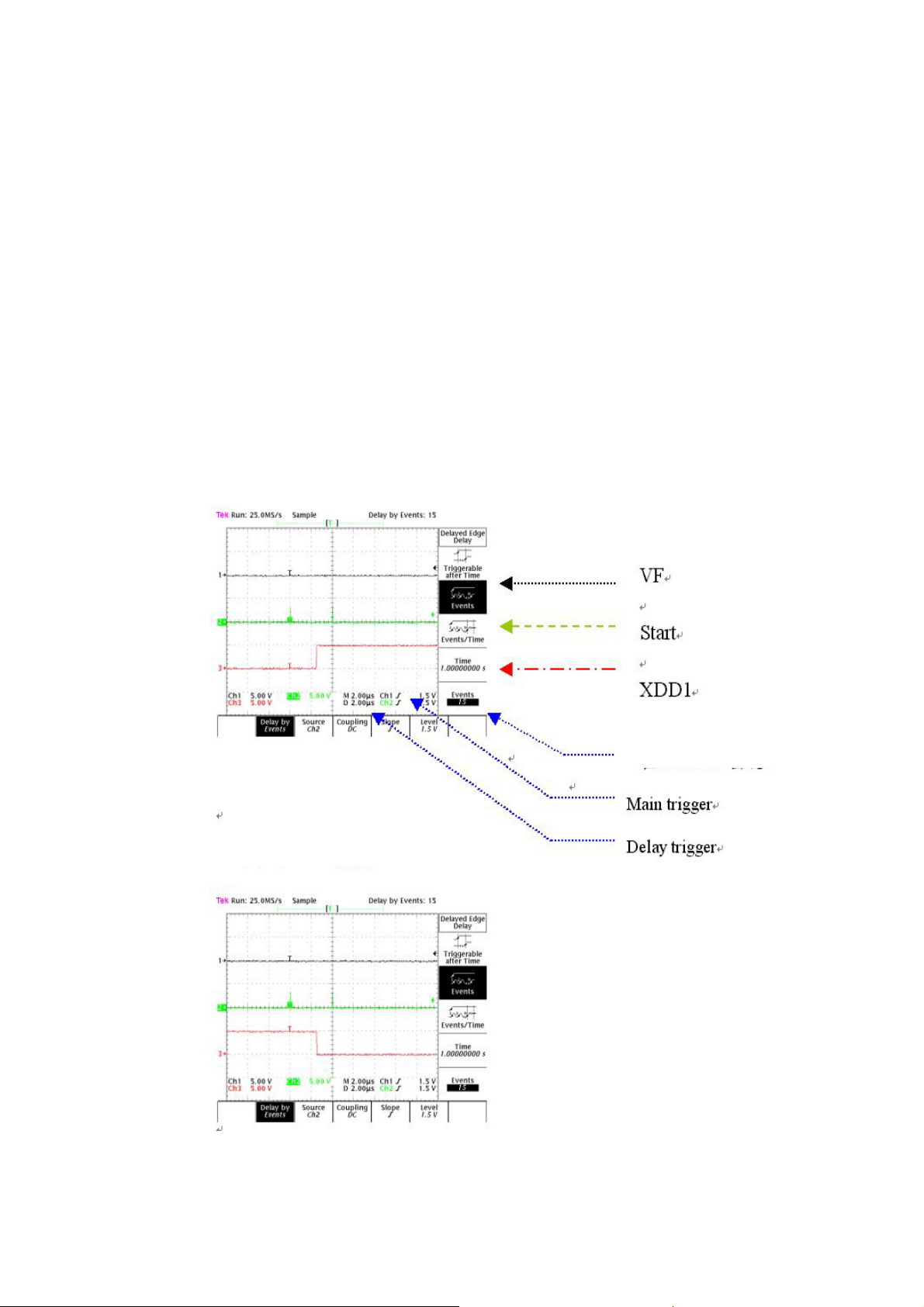
a-4 Check the output of X and Y :
As Fig. 8 shown. Confirm that the waveform is normal.
X : DD1 Waveform
X : DD2 Waveform
Event =15 ,means that
ulse shown at block15
Fig.8 X : DD1 and DD2 output waveform
26
Page 28
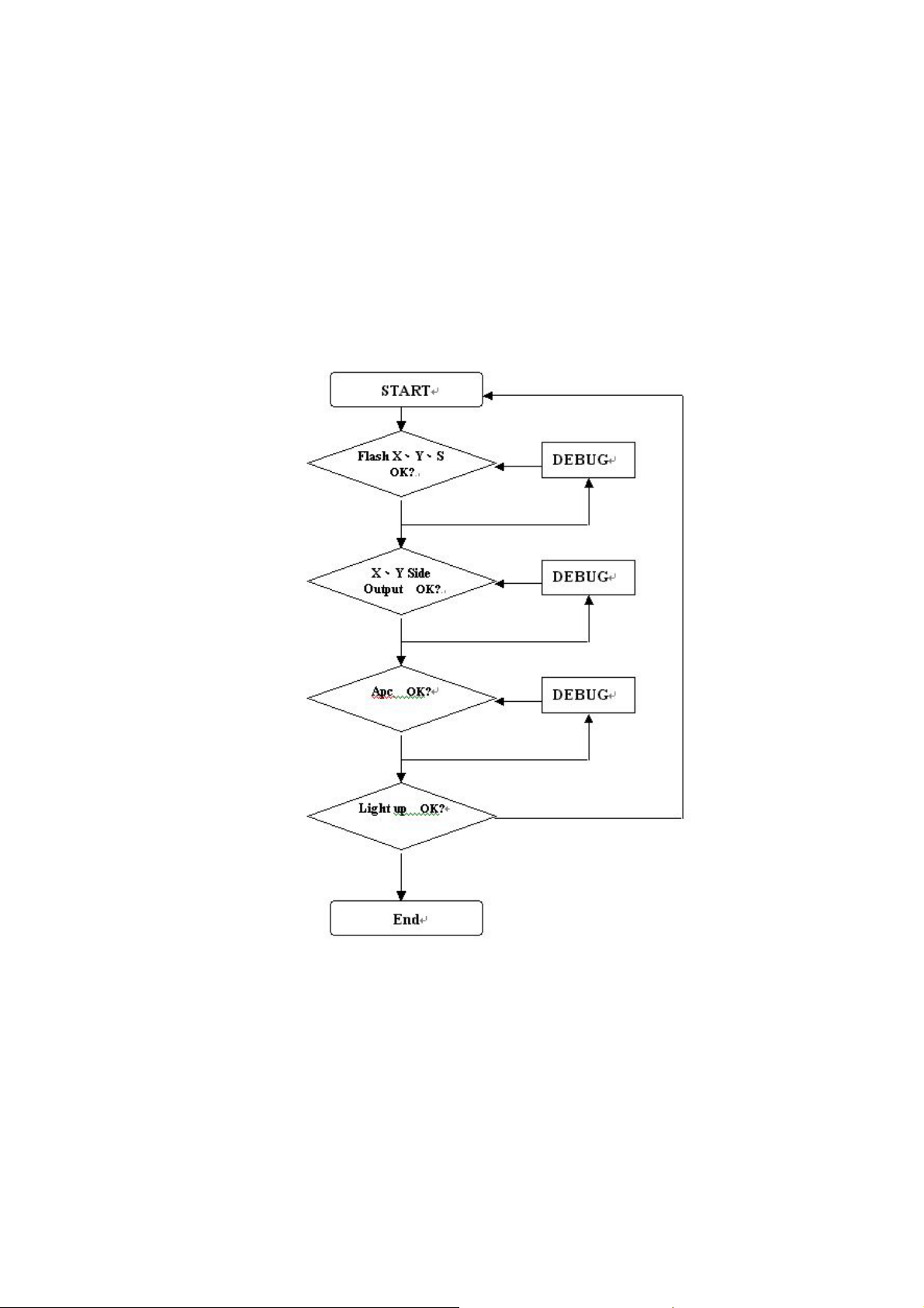
b. Checking the function of APC:
b-1 The data of Adat are normal. Compared with look up table(LUT).
b-2 Checking the power of WAPC , Check the signal of SM and SF0 to make sure the power
WAPC functions OK.
b-3 Check the screen of PDP :
From the screen to check the functions of DIF’s performance is good or not.
c The debug flow chart as Fig.9 shown.
Fig.9 The debug flow chart
2.2.4 Advanced testing and checking:
The DIF board has three major functions.
a. Image signal process:
a-1 Purpose: To check the functions of image signal process are correct.
As Fig.10 shown ,
27
Page 29
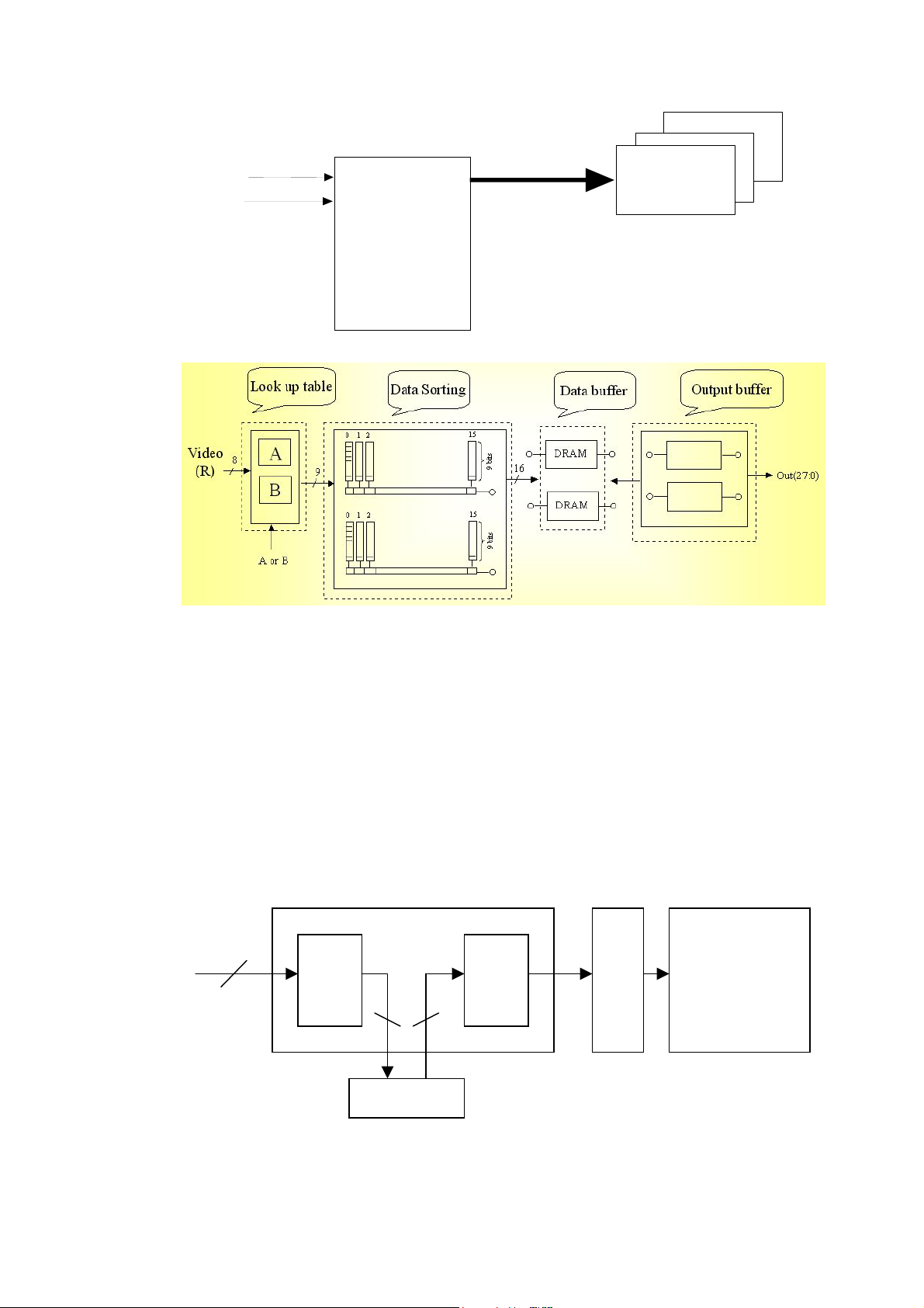
data
buffe
age
source
a
ce
compute
deo
r
vi
Antenna
r
RAM
im
interf
Fig.10 Image signal process
a-2 As Fig.11 Shown , the image signals separated into R , G , B for processing.
Fig.11 Image signal process
a-3 Here we check the input / output signals is correct or not. Compared with the output
and input waveforms of Rx7-Rx0 , Gx7-Gx0 , Bx7-Bx0 are the same or not , and check
the waveforms of Vx , Hx , Blkx , BlkVx , Clkx are normal or not .
a-4 For IC101-103 , IC106 is passing a Wp signal to IC101-103 , as fig.11 image signal
process , IC101-IC103 output signals to panel , so the buffer and extension board ,
connector are checking points too.
a-5 Image process
EX : IC101 –> PANEL Output
IC101
LUT
7-9
8-9
Driver IC
Panel
In IC101 , There are 7 blocks for processing , from system trigging to output signal.
DRAM
28
Page 30
For example ,the process of VF signal as below shown:
V
The real waveform is as below , the length is 60μS.
VF
V
Fig.12 Real waveform
Ex : IC100 –> IC106
μ-com
VF
SRAM IC104 IC100 PMC
IC106
29
Page 31

Ex : Dividing panel into 30*28 , store the data into SRAM.
IC104 not only calculate the block sum , scan sum , total sum but also deal with the
Pattern A , pattern B , pattern judgment of the pattern check. The value of calculation
will be sent to up1 for operation . In the checking of buffer , we only compare the
waveforms between input and output.
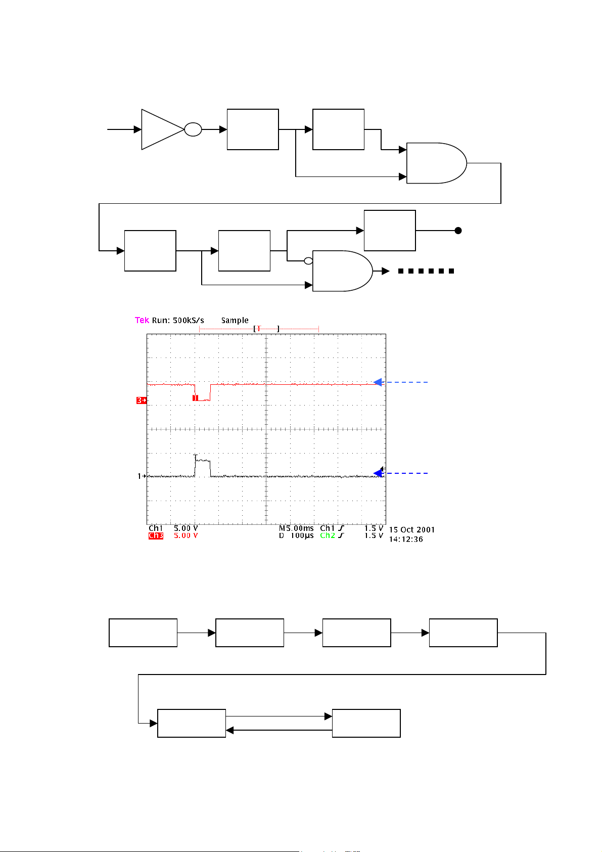
b. Waveform controlling :
SRAM
b-1 Purpose : To check the waveform of X , Y is normal or not.
These parts of functions are accomplished by IC 106 to control the sustainer of
Fig.13 Driving signal (Sub-fielb period T Sfi)
X and Y. The controlling waveform is stored in IC170 and IC171 , that’s FlashX
and FlahY , the waveform is as Fig.13 shown.
30
Page 32

b-2 List of signal input
R Red Data Pixel_Red Data
G Green Data Pixel_Green Data
B Blue Data Pixel_Blue Data
CLK Clock dot clock
HD H_sync Horizontal synchronous
VD V_sync Vertical synchronous
BLK Blank blanking-invalid data period
EN Enable display enable
31
Page 33

b-3 Timing spec. – see with video signal input time chart
b-4 Sub-field:
Start End
The real information is:
1-SF 2-SF 3-SF 4-SF 5-SF 6-SF 7-SF 8SF 9-SF
SF0
SF1
SF1
SF2
c. Auto Power Control (APC):
c-1 Purpose : To check the functions of APC are normal or not.
The functions of APC are important to panel ; it may cause power failure or even
panel broken . The processing is as Fig.14 shown:
Fig.14 APC block diagram
32
Page 34

c-2 When signal data send to APC , the Calculate Display Ratio begins to calculate the ratio
of pattern .After checking and calculating pattern(A ,B , C) , the numbers of pattern , then
sending the data of display and switching count to the window memory .
Fig.15 Pattern A , Pattern B , Pattern C (CPT thousand-birds’ pattern)
c-3 The APC is performing mathematical calculations , by reducing the sustain frequency and
closing some sub-fields to accomplish. There is reference for judgment , as Fig.16 and Fig.17
shown . The parameters has been tested by experiments to determine , so if the parameters of
APC are not the optimal parameter , it may cause panel broken , scan IC burned , power supply
failure.
Fig.16 The curve of APC
33
Page 35

Fig.17 The limit of power vs. sustain frequency
c-4 The debug flow chart is as Fig.18 shown.
Fig.18 APC debug flow chart
34
Page 36

c-5 According to the past experiences , most of the errors of APC happened at SRAM and
buffer IC , so these parts will be the checking points.
2.2.5 IC100 - IC106 : Main signals measurement
Purpose : To check the action of FPGA from IC100 to IC106
The waveform is shown as below.
a. Take the Wp waveform as examples:
2. Observe
ch2 signal
1. Trigger
ch3 signal
a-1 Explanation of waveform :
1. Trigger
ch1 signals
2. Observe
ch2 signals
3. trigger
level
4.ch2 waveform
The scanning waveforms look correctly.
35
Page 37

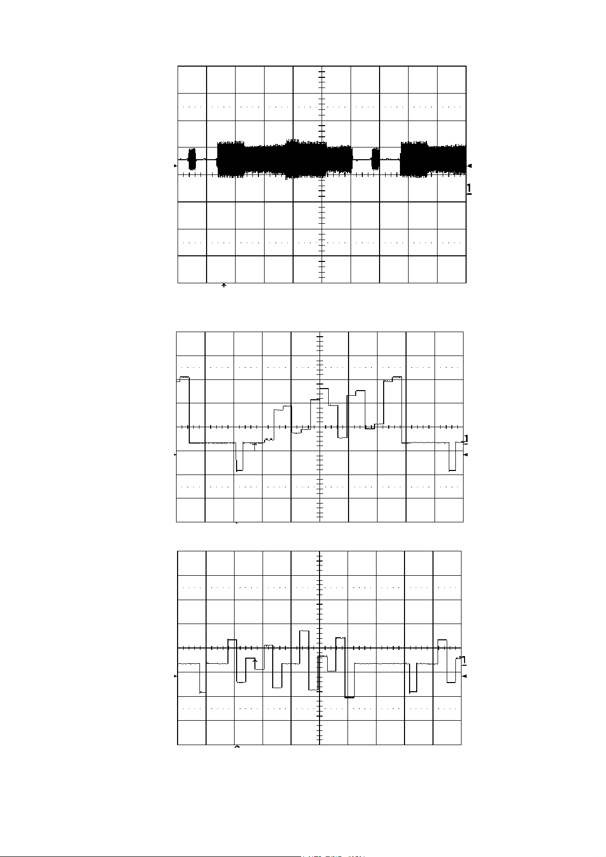
b. The controlling waveforms of IC106 are checking below signals(CH3 trigger V signals):
V、Start、Wp、Wn、SF0~SF3、Esq
Test Pattern=Random
Main
signal
1
Singal
Name
V
P41(V
Remark
)
D
Make sure the DIF input signal of V signal is correct , and is the
trigger signals.
2
Wp
TP121
(Wp)
36
Page 38

3
Wn
TP123
(Wn)
4
5
SF0
SF1
TP126
(SF0)
TP127
(SF1)
37
Page 39

6
SF2
TP128
(SF2)
7
8
SF3
Esq
TP129
(SF3)
TP125
(ESQ)
38
Page 40

c. Checking the outputs of X and Y sustainer board
Make sure the waveform of X/Y are correct , the reference waveforms as below
( CH3 trigger V signals)
Test Pattern=random
IC106_Signal List
X
-side
1
Signal
Name
XSI1
Pin No
TP143
2
XTSC
TP141
39
Page 41

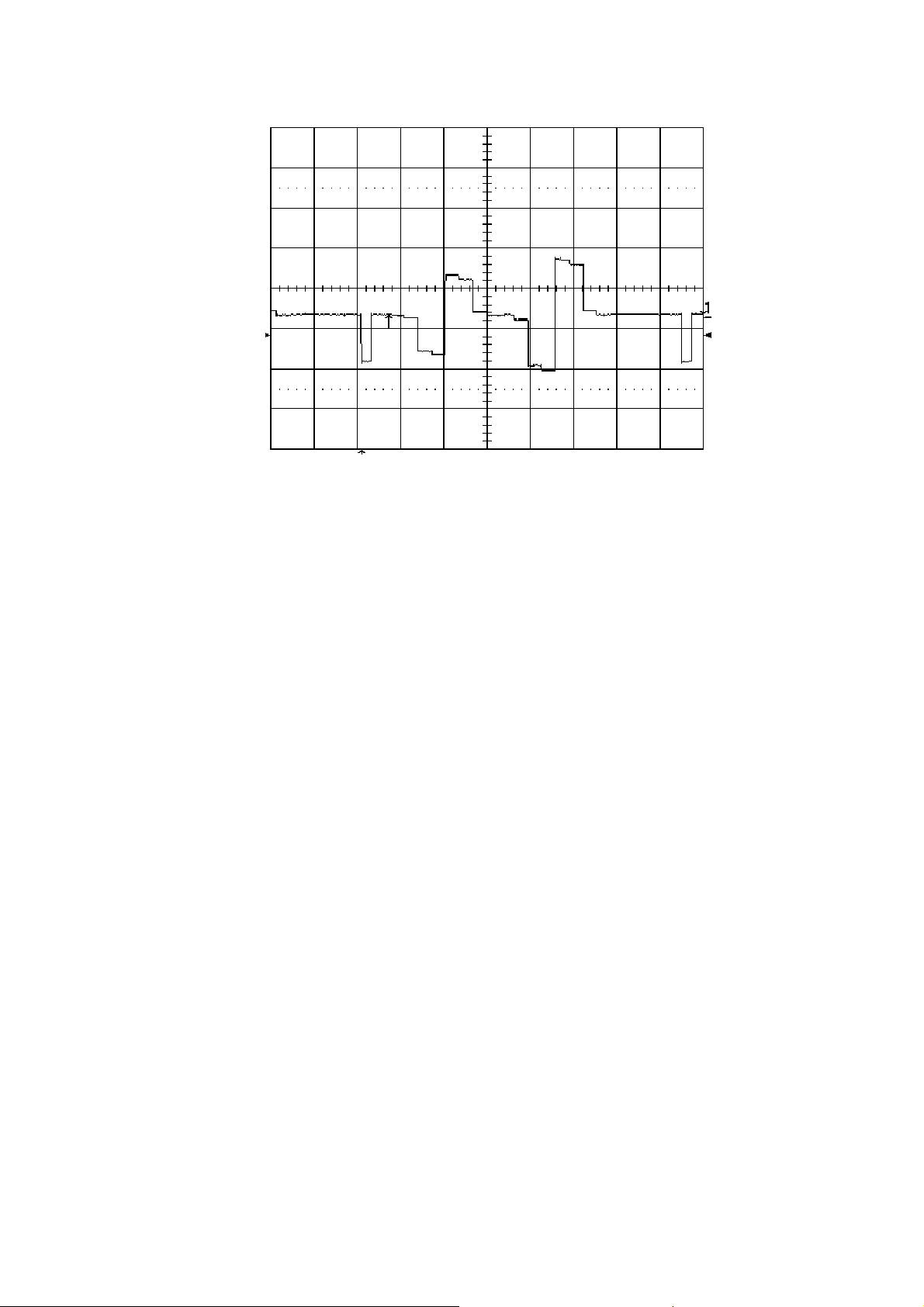
3
XSTB
TP142
4
5
XLE
XSI2
TP144
TP145
40
Page 42

6
XCLK
TP146
7
8
XNEH
XNEL
TP147
TP148
41
Page 43

9
XEFH
TP149
10
11
XEFL
XAEH
TP150
TP151
42
Page 44

12
XAEL
TP152
13
14
XSU
XG1H
TP133
TP134
43
Page 45

15
XG1L
TP135
16
17
XG3L
XG2L
TP136
TP137
44
Page 46

18
XP2L
TP138
19
20
XDD1
XDD2
TP139
TP140
45
Page 47

Y
-side
1
YSC2A J7-PIN2
YSC1A J7-PIN3
2
YNELA J7-PIN5
3
46
Page 48

YNEHA J7-PIN6
4
YEFLA J7-PIN8
5
6
YEFHA
J7-PIN9
47
Page 49

YSC2B J7-PIN11
7
YSC1B J7-PIN12
8
YNELB J7-PIN14
9
48
Page 50

YNEHB J7-PIN15
10
YEFLB J7-PIN17
11
YEFHB
12
J7-PIN18
49
Page 51

d. The function of APC checking, reference waveform as below (Aclk is trigger signals,Adata is
checking signals)
Test Pattern=Pattern A
Pin
Signal Name
Adata&
1
Aclk
No
TP21
&
TP24
( Complete thousands_birds )
Checking point
1-a
50
Page 52

1-b
1-c
2 SM&W
P
TP130
&
TP121
51
Page 53

e. IC100
Make sure the waveforms of IC100 is normal or not.(CH1 trigger V signal)
IC100_Signal List
Test Pattern=Pattern A ( Complete thousands_birds )
1
Singal
Name
Rx7-
Rx0
Pin No
P7-14
Remark
2 Gx7-Gx0
P15-19、
24-26
52
Page 54

3 Bx7
P27-31、
26-38
4 Vx P39
5 Hx P40
53
Page 55

6 BLKx P41
7 CLK 321 P46
8 CLK 324 P47
54
Page 56

9 R7-R0
P111-116、
119-120、
P122、
10 G7-G0
P135-136、
11 B7
125-128、
131-133
139-144
55
Page 57

12 HD P148
13 VD P149
14 BLK c P150
56
Page 58

f. IC101
Make sure the waveforms of IC101 is normal or not.(CH1 trigger V signal)
IC101_Signal List
Test Pattern=Pattern A ( Complete thousands_birds )
Singal
Name
RAD27 P7
1
Pin No Checking point
RACLKa P45
2
RACLKb P46
3
57
Page 59

SF0-SF3 P53-56 Same as (a)
4
5
6
7
WN P57 Same as (a)
WP P58 Same as (a)
BLHR P60
58
Page 60

VFR P62
8
HPR P63
9
10
VPR P64
59
Page 61

11
Rx7 P75
12
13
SM P86
RMBD0 P87
60
Page 62

RMBOE P111
14
RMBWE P112
15
RMBCS1 P113
16
61
Page 63

RMBRS P115
17
RMBA0 P116
18
RMAD0 P132
19
62
Page 64

RMAOE P158
20
RMAWE P159
21
RMACS1 P160
22
63
Page 65

RMARS P162
23
RMAA0 P174
24
25
RFI8 P192
64
Page 66

26
Vx P205
27
BLKx P207
g. IC104
Make sure the waveforms of IC104 is normal or not.(CH1 trigger V signal)
IC104_Signal List
Test Pattern=Pattern A
Singal
Name
( Complete thousands_birds )
Pin No
65
Page 67

1
EW P144
2 CLK324 P183
h. gamma flash and up2
The gamma functions can check with VIF , select the low , medium , high color temperature to see the
changes.
66
Page 68

2.3 POWER Board:
2.3.1 Introduction:
VXG
VF VCCVS
VSB
VW
Explanation :
Input voltage is from AC100V to 240V , frequency 47HZ~63HZ is available.
The maximum input AC voltage range is from 90V to 265V .
2.3.2 Output Power rating :
Voltage Adjustment
Danger ! High Voltage
VAU
Name Peak load
Vsb 5V 0.4A
Vdd 5V 2.0A
Ccc 5V 3.0A
Vau 9V 1.7A
Vfan 12V 0.5A
Vf 15V 0.6A
Vs 170V 290W 50A
Vw 65V 80W 6A
Vxg -160V 0.1A 1A
Vaux 310~380V 65W
Output Max Load
2.3.3 pin assignments of connectors
67
Page 69

a. Connector ; AC IN
Pin-No Name Voltage
1 AC 100~240V AC
2
3 AC 100~240V AC
b. Connector ; PD
Pin-No Name Voltage REMARK
1 Vcc 5V
2 Vcc 5V
3 VccG ( Vcc GND ) LV Ground
4 VccG ( Vcc GND ) LV Ground
c. Connector ; PX1
Pin-No Name Voltage REMARK
1 Vs 175V
2 NC
3 VsG Vs GND HV Ground
4 VwG Vw GND HV Ground
5 Vw 65V
6 Vf 15V
7 VfG (Vf GND) HV Ground
d. Connector ; PX2
Pin-No Name Voltage REMARK
1 Vcc 5V
2 VccG ( Vcc GND ) LV Ground
3 VxgG ( Vxg GND ) HV Ground
4 NC
5 Vxg -160V
e. Connector ; PY
Pin-No Name Voltage REMARK
1 Vs 175V
2 NC
3 VsG (Vs GND) HV Ground
4 VwG (Vw GND) HV Ground
68
Page 70

5 Vw 65V
6 Vf 15V
7 VfG (Vf GND) LV Ground
8 Vcc 5V
9 VccG (Vcc VGND) LV Ground
f. Connector ; Vaux
Pin-No Name Voltage
1 Vaux DC( + ) 300~380V ( primary)
2
3
VauxG DC( 一 )
Vaux G ( primary )
g. Connector ; PW
Pin-No Name Voltage REMARK
1 Vw 65V
2 Vw 65V
3 NC
4 VwG ( Vw GND) HV Ground
5 VwG (Vw GND) HV Ground
6 Vcc 5V
7 VccG (Vcc GND) LV Ground
h. Connector ; PV
Pin-No Name Voltage REMARK
1 Vau 9V
2 Vau 9V
3 VauG VIF GND VIF Ground
4 VauG VIF GND VIF Ground
5 Vdd 5V
6 Vdd 5V
7 VddG VIF GND VIF Ground
8 VsbG VIF GND VIF Ground
9 Vsb 5V 0.4A
i. Connector ; OH
Pin-No Name Voltage REMARK
1 OH Dry Contact
2 COM OH GND Connect to VccG
69
Page 71

j. Connector ; FAN1 FAN2
Pin-No Name Voltage REMARK
1 Vfan 12V
2 Fan_STS Fan Status
3 VfanG 12V GND FAN Ground
k. Connector ; CN
Pin-No Name Voltage REMARK
1 Vsb +5V Input Signal Voltage
2 VCC__ON 0V/OPEN Input Signal (O.C.)
3 Reserved
4 HV_ON 0V/OPEN Input Signal (O.C.)
5 Reserved
6 Vsb GND VGND VIF Ground
7 FLT 0V/OPEN Output Signal (O.C.)
8 PWRLOSS 0V/OPEN Output Signal (O.C.)
9 FAN _OK 0V/OPEN Output Signal (O.C.)
10 Vsb GND Vsb GND VIF Ground
2.3.4. Troubleshooting
a. Plug out CN connector but no Vsb voltage : Replace IC101 0254(TNY264P).
b. Vaux not enough 300~380 voltage : Replace IC001 FA5332 ; Q003 K2698 ; Q004 K2698 ;
R028 100Ω ; R030 100Ω.
c. Vcc , Vdd no 5 voltages : Replace IC201 M51995 ; Q201 K2717 ; R201 0.22Ω
3W.
d. Vw no 65 voltage : Replace IC301 M51995 ; Q301 K2717 ; R301 0.18Ω 3W.
e. Vs no 175 voltage : Replace IC501 M51995 ; Q501 K2607 ; Q502 K2607 ;
R511 0.22Ω 3W ; R512 0.22Ω 3W.
f.Vxg no –165 voltage : Replace Q703 K2638 ( Under Vs is normal )
g. The adjustment of all voltage : VR
5V…..…….1A…….….VR151 5V……..…5A…….…...VR253
15V…..…0.5A…..……VR251 9V……...1.7A…………VR252
65V……..1.7A………..VR351 175V……...2.5A…………VR551
160V…….0.1A……….VR751
70
Page 72

2.4 X-Sustainer board:
2.4.1 X-Sustainer board’s pin alignment :
a. Input Vlotage
Name Input Voltage Current(mA) Remark
Vcc 5 240
Vf 15
Vs 170 1.2A Normal 1.0~1.5A
Vxg -160 40
Vw 65 40
Vs 170 1.2A Normal 1.0~1.5A
Vxg -160 40
Vw 65 40
b. Photo of X sustainer :
J7:(VXDD-VXG)70
J3: W-side
70(全白)
R407: J7 VR
Normal 40~150mA
J6:(VXE-GND)60V
R417: J6 VR
J1:X-side
PX2:VXG,VCC input
J302:X-side
PX1:VF,VW,VS input
J301:X-side
output
c. Input signals: DIF-X sustainer 30 lead 5V TTL signal
71
Page 73

d. Output signal :
d-1 Output to PDP
Above figure shows the waveform from X and Y extension board(TP301~TP308)
; Green line is the X-side output and Red line is the Y-side output.
d-2 Output to W-extension board :
Vw 65V DC
2.4.2 X-side function explanation :
Low voltage and High voltage
There are two kinds of low voltages : 5V and 15V . They are used to provide the input
signals of driving waveform .
5V signal : Providing the power of ICs . The TC4426 and IR2113S(Driver IC) are for
driving MOS FET. IC :MC74244 and HCPL-M611 , provide signals to scan IC.
So the 5V of X sustainer includes the power of driver IC and input signals and DC
5V adapter.
15V signal : Providing the power of TC4426 and IR2113S , the input signals of 5V
switching to 15V to drive the signal of MOS. So we can check the 15V
only at the output of driver IC and the input of MOSFET(VG).
65 Voltage : The voltage of Vxe(Vw) at X-side is 65 voltage .There are two groups of
circuit: one generates 65V to get the waveform of NAMARI , the other
provide 65V for COF of W-side .
The 65V of Vysc of Y-side generates 35V at the address period of bulk-side.
High voltage:170V and -160V belong PDP high drive voltage.
170 Voltage: The control signals of EFH , EFL , NEH , NEL , XSU (170V)are generated
by the MOSFET after MOSFET got a control signal from GATE pin.
72
Page 74

Resister : 820Ω / 3W x 6 pcs . For generating the positive exponential
waveform.
High-speed diode: C16T40F; D104 , D106 , D204 , D206 , D123 , D124
, D125 , D126 , D127….. etc。
-160 Voltage : Using for generating two negative exponential waveforms , the control
signals of XG1L , XG2L , XP2L , XG3L to drive –160V let the MOSFET
to generate waveforms.
Resister : 390Ω / 3W , 820Ω / 3W . For generating the negative
exponential waveforms.
2.5 Y-Sustainer board:
2.5.1Y-Sustainer pin alignments :
a.Input voltage ::
Name Input Voltage(VDC) Current(mA) Remark
Vcc 5 240
Vf 15 70(Full white) Normal 40~150Ma
Vs 170 1.2A Normal 1.0~1.5A
Vysc 65 8
Vw 65 40
b. Photo of Y sustainer :
J301:Y-side output
to Y- upper
extension board
J1:Y-side input
voltage :Vcc , Vf ,
Vs , Vysc ,Vw
R417: VR
J302: Y-side
output to Y- lower
extension board
J3:W-side 20PIN
signals input
73
Page 75

c. Input signals : DIF-Y sustainer 20 lead 5V TTL signa
d.Output signal :
d-1 Output to PDP
C414:40
V 輸出接
Above figure shows the waveform from X and Y extension board(TP301~TP308)
; Green line is the X-side output and Red line is the Y-side output.
2.5.2 Y-side function explanation :
The driving methods are the same of X and Y . The 5V signals from DIF board through
IR2113 and TC4426 transfer to 15 V to drive MOSFET to generate waveforms.
There are two kinds of low voltages : 5V and 15V . They are used to provide the input
Signals of driving waveform .
5V signal : Providing the power of ICs . The IR2113S(Driver IC) are for driving the
MOS FET of Y-side.
15V signal : Providing the power of TC4426 and IR2113S , the input signals of 5V
switching to 15V to drive the signal of MOS. So we can check the 15V
only at the output of driver IC and the input of MOSFET(VG).
65 Voltage :The 65V of Vysc of Y-side generates 35V at the address period of bulk-side.
170 Voltage: The control signals of EFH , EFL , NEH , NEL , XSU (170V)are generated
by the MOSFET after MOSFET got a control signal from GATE pin.
High-speed diode: C16T40F; D104AB , D106AB , D204AB , D206AB
74
Page 76

3. PDP repairing flow-chart
Q
N
N
N
N
k
3.1 Main flow-chart :
on-warranty
Repair
CPT responsibility
Defective PDP
Judgment
Can not repair
Customer responsibility
Can repair
Repair ?
Warranty ?
What’s wrong
on-warranty
ot repair
Panel screen
defect
Replace Module
Power failure
Disassemble and
Check
Replace PCB
Adjustment
A Test
Repair Center
ext flow
chart
Signal failure
Disassemble and
Chec
Check debug
flow chart
Customer
75
Page 77

3.2 Debug Flow chart : 1 No screen
N
N
N
N
N
N N N N N
N
N
Plug out connector
PV/ CN , Check
CN connector= 5
volts(1+ , 6 - ) ?
Y
Power OK ?
Y
PDP switch ON ?
Y
Stand-By Red light OK
N
AC inlet Fuse burned ?
Open back cover
Power board Fuse burned ?
Y
Replace Fuse
CFM Power cord OK
Turn on power switch
Y
Replace Fuse
Y
Y
Replace VIF board
Replace power board
Plug out PX1,PX2,PY one by
one to check X /Y board OK?
Check the signals from
DIF to X,Y,W board ?
Check CN connector= 5 volts(1+ , 6 - ) ?
Y
Voltage = 4.9V ~5.3V ?
Y
Check PD connector= 5 volts(1+ , 4 - ) ,Power on
to check voltage = 4.9V~5.3V ?
Y
PD voltage from 5V drops to 0V ?
Y
Plug out the PY,PX1,PX2 one by one and
After power on can not start PD voltage ?
Y
Adj. VR151 make
Voltage = 4.9V ~5.3V
Adj. VR253 make
Voltage = 4.9V ~5.3V
Y
Replace DIF board
76
Page 78

3.3 X sustainer malfunction repairing flow-chart
77
Page 79

78
Page 80

79
Page 81

80
Page 82

81
Page 83

3.4 Y sustainer malfunction repairing flow-chart
82
Page 84

83
Page 85

84
Page 86

85
Page 87

4. Common defect debug:
4.1 Screen dark and flickering :
a. Phenomenon :
b. explanation :
b-1 At first figure shown , the second “namari” waveform is dropped under 170 volts , but the
first “ namari “ waveform is normal . It is related to the sequences of switching operations:
AEH , AEL , XSU .
b-2 Checking above waveforms , found that the waveform of XSU from MOSFET is abnormal.
b-3 As the second figure shown , blue curve is the control signal from the input of XSU driver
86
Page 88

IC , green curve is output of 15V driving MOSFET , we have seen that the voltage had
dropped causing the second “namari” waveform don’t work.
b-4 Correction : Replace the IR2113S DRIVER IC .
4.2 170v Limit current
a. Phenomenon :
The voltage can not adjust to 170V .Checking all the input signals are normal , driving Ics
normal , but the MOSFET Q123 has no output , it maybe the failure from XEFH circuits.
b. Explanation :
b-1 The voltage can not adjust above 170 volts , but the negative waveform is normal after
applying the –160 voltage.
b-2 It should be wrong with the sustain pulse generator circuits , from the outputs of MOS ,
found that the Q123 had no output by the IC121 controlling .
b-3 There is signal from driver IC IR2113 , but no Vsg.
b-4 Shut down the power , measuring the D/S pin of Q123 through multi-meter the resister
is only 22 ohms , normal is open , so it was breakdown .(type MOSFET IRFP460A)
b-5 Replace a new MOSFET Q123 ,then OK.
4.3 Some phenomenon of failure PCB boards :
a. DIF: Noise on the screen , no screen。
b. VIF: Missing color , poor color steps , no sound , no screen (OSD OK)
c. POWER: No screen , PCB no power.
d. X-Sustainer: No screen , Color not enough , Screen flickering , When connect to PMC ,
Can not change pattern.
e. Y-Sustainer: Screen dark , but video OK
(DIF+VIF+POW+X-Sus = “screen dark” means DIF+VIF+POW+X-Sus OK)
f. Audio Bard: No sound , power input : DC :300〜380V
g. X-sustainer : No screen .
h. Y-Sustainer : Screen dark .
i. X-extension board abnormal :
dark screen
Bright screen
Bright screen
87
Page 89

j.Y-extension board abnormal:
dark screen Bright screen
5. Debug / Inspection :
5.1 Debug :
5.1.1 X-sustainer board:
a. According to the X-sustainer board debug flow chart , applied the electrical power to check
the condition is normal or not.
b. Using multi-meter to check the J6 connector DC output(Gnd-VXE) is 60 volts or not, if not
then adjust the VR147 to 60 volts.
c. Using multi-meter to check the J7 connector DC output(VXG-VXDD) is 70 volts or not, if not
then adjust the VR407 to 70 volts.
d. Check the screen is normal or not; Change pattern to full white and thousands_birds to check
the power is normal or not.
e. After screen lighting for 5 minutes, Check the heat-sink of the MOSFET at the X-sustainer board
, the temperature should be around 50 degree C.
5.1.2 Y-sustainer board:
a. According to the Y-sustainer board debug flow chart , applied the electrical power to check
the condition is normal or not.
b. Using multi-meter to check the J5 connector DC output(VYSC-GND) is 40 volts or not, if not
then adjust the VR147 to 40 volts.
c. Check the screen is normal or not; Change pattern to full white and thousands_birds to check
the power is normal or not.
d. After screen lighting for 5 minutes, Check the heat-sink of the MOSFET at the X-sustainer board
, the temperature should be around 50 degree C.
5.2 Inspection :
PDP SET inspection items after finishing repair :
Item Classified Inspection item Method Remark
1
2
Appearance Back cover screw shortage Eye view
Appearance Screen Filter scratch Eye view
3
4
5
6
7
Appearance Terminal loosing Eye view
Reliability voltage / frequency variation POWER SUPPLY
Reliability Hi-pot test Hi-pot tester
Reliability AC-INLET hi-pot test Hi-pot tester
Screen Position /Width Eye view
88
Page 90

8
Screen H/V resolution / saturation Eye view
9
10
11
12
13
14
15
16
17
18
19
20
21
22
23
24
Screen H/V stability Eye view
Screen Hue / Color Eye view
OSD AUDIO-Mute/ Balance Eye view/remote
OSD INPUT-PC1 / HDTV / AV1 / AV2 Eye view/remote
OSD VIDEO-Color Temp / Gamma Eye view/remote
OSD VIDEO-Brightness / Contrast Eye view/remote
OSD FUNCTION-Information / Default Eye view/remote
OSD DISPLAY-Aspect Ratio / Zoom Eye view/remote
Signal/terminal Factory default / key-pad function Eye view
Signal/terminal PC TIMING/ TUNNER Eye view
Signal/terminal D-sub / DVI Eye view
Signal/terminal AV / S-video Eye view
Signal/terminal VIDEO / Component / PC AUDIO Eye view
Signal/terminal D-SUB/ DVI-I / RS-232 Eye view
characteristic
characteristic
White balance(△x) / (△y) / (△Y) / contrast
Power consumption Power meter
CA-100
89
Page 91

6.BOM list:
6.1 PDP PCB board BOM list :
NO. Item no. Description/specification Remark
1 4359011400 X-SCAN SU ASSY PCB 46"WVGA V00
2 4359021400 X-EXT. U ASSY PCB 46"WVGA V00
3 4359041400 X-EXT. L ASSY PCB 46"WVGA V00
4 4359111400 Y-BULK SU ASSY PCB 46"WVGA V00
5 4359121400 Y-EXT. U ASSY PCB 46"WVGA V00
6 4359141400 Y-EXT. L ASSY PCB 46"WVGA V00
7 4359211400 W-EXT. L ASSY PCB 46"WVGA V00
8 4359221400 W-EXT. R ASSY PCB 46"WVGA V00
9 4359301400 DIF ASSY PCB 46"WVGA V00
10 4322500001 FFC CABLE X-DIF 30L 46"WV-V00
11 4322500002 FFC CABLE Y-WEL 20L 46"WV-V00
12 4322500003 FFC CABLE DIF-WER
13 4322500004 FFC CABLE WEL-WER
14 4313514001 POWER SUPPLY MPF7701
15 4359401401 ASSY PCB PC1 V00
16 4359401402 ASSY PCB PC2 V00
17 4359491401 ASSY PCB VIDEO PW2.5-VD
18 4359441401 ASSY PCB AUDIO
19 4359421401 ASSY PCB REMOTE FRONT PAD
20 4359431101 ASSY PCB KEY PAD
21 4359411401 LINE FILTER ASSY PCB
6.2 BOM: DIF
NO Item No. Part No Assignment Remark
1 4322000007 MC74ACT541DTR2 IC8-IC21 buffer
2 4322403004 FF038OSA1-2000 J3&J5 Connector
3 4322401001 52610-3090 J7 Connector
4 4322403002 FH12-45S-0.5SV J8 Connector
6.3 BOM :Video Module
90
Page 92

NO Item No. Part No Assignment Remark
1 UPD64083GF-3BA 4322090012 U3C
2 49US/20PF/40/+-30ppm 4321500010 Y1B(24.576MHz)
3
4 H354LAI8113 4323201001 FIL1C FIL2C
5 LM1117MPX-2.5V 4322100006 U1C
6 LM1117MPX-3.3V 4322100004 U2C
7 NJM2244M 4322090013 U2D
8 NJM2267M 4322090014 U1D
9 MMBT3904 4321490001
10 MMBT3906 4321490002 Q1C Q3C Q4C Q5C Q7C Q8C Q10C Q12C Q15C
11 SAA7118E/V1 4322200001 U1B
12 49US/20PF/40/+-30ppm 4321500005 Y1C(20MHz)
13 RJ-1078 white stand 4322404004 JP4A
14 RJ-1086 red stand 4322404005 JP3A
15 RJ-1086 yellow stand 4322404006 JP1A
Q1A Q1B Q1D Q2A Q2C Q2D Q3A Q4A Q5A Q6A
Q6C Q7A Q8A Q9A Q9C Q11C Q13C Q14C
16 JY-5042 4322404003 JP2A
6.4 BOM : VIF Main Board
91
Page 93

NO Item No. Part No Assignment Remark
1 MMBT3904 4321490001 Q3 Q7 Q15 Q8 Q10 Q12
2 MMBT3906 4321490002 Q6
3 49USM/20PF/40/+-30ppm 4321500009 Y2,Y3(16.257MHz)
4 49USM/20PF/40/+-30ppm 4321500005 Y1(20MHz)
5 74LCX16374MEAX 4322000013 U22,U24
6 74LCX244MTCX 4322000014 U21,U23
7 74VHC123AMTCX 4322000015 U6
8 NC7SZ126P5X 4322000016 U7 U8
9 74LVX273MTCX 4322000017 U25
10 AD9888KS-140 S-128 4322005005 U3
11 NM24C02M8X 4322007022 U1
12 NM24C16M8X 4322007023 U18
13 SII504CM208 4322090007 U11
14 HY57V64322CT-7 4322800003 U12
15 LM1117-1.8V 4322100005 U13
16 LM1117DTX-3.3 4322100004 U10 U29 U4 U28 U4001 U5 U27
17 LM317M
18 AT49BV8192AT-12TC 4322007024 U15
19 ICS501
20 NJM2700G SOP40 4322090011 U32
21 PIC16C63A-20 4322090010 U33
22 PW171-20U 4322090009 U19
23 LT1381A
24 SII153BCT100 4322090006 U9
25 TEA6320T/V1 4322090008 U31
26 V6300L 4322090003 U20
U16 U17
U30
U2
6.5 BOM:POWER SUPPLY
92
Page 94

NO Item No. Part No Assignment Remark
1 IC 0254 IC 101 TNY264P
2 IC FA5332 IC 001
3 IC M51995 IC 201
4 IC M51995 IC 501
5 2SK 2698 Q003
6 2SK 2717 Q201
7 2SK 2607 Q502
8 2SK 2638 Q703
9 2SK 2607 Q501
10 2SK 2717 Q301
11 0.22-3W R201
12 0.18-3W R301
13 0.22-3W R511
14 0.22-3W R512
15 10-5W R004
16 10-5W R005
17 10-5W R070
18 10-5W R551
19 10-5W R552
20 10-5W R553
21 0.18-3W R024
22 0.183W R025
23 0.18-3W R026
24 PQ30RV11 IC252
25 PQ30RV31 IC253
26 PQ12RD11 IC151
27 TA76431S IC551
28 PC123FY8 PC004………… PC502
29 ICP-N15 ICP201
30 PC017 PC254……… PC735
31 600V.10A YG912S6 D017 D018
6.6 BOM:X sustainer board
93
Page 95

NO Item No. Part No Assignment Remark
1 IR2113S 4322005002 IC121A
2 IR2113S 4322005002 IC121B
3 IR2113S 4322005002 IC231
4 IR2113S 4322005002 IC241
5 TC4426 4321405004 IC101A
6 TC4426 4321405004 IC101B
7 TC4426 4321405004 IC141
8 TC4426 4321405004 IC151
9 TC4426 4321405004 IC171
10 TC4426 4321405004 IC181
11 TC4426 4321405004 IC201A
12 TC4426 4321405004 IC201B
13 HCPL-M611 4322004001 PC31
14 HCPL-M611 4322004001 PC32
15 HCPL-M611 4322004001 PC33
16 HCPL-M611 4322004001 PC34
Low Volts
Low Volts
Low Volts
Low Volts
Low Volts
Low Volts
Low Volts
Low Volts
Low Volts
Low Volts
Low Volts
Low Volts
Low Volts
Low Volts
Low Volts
Low Volts
17 HCPL-M611 4322004001 PC35
18 HCPL-M611 4322004001 PC36
19 DC-302R 4322100002 P451
20 HC244 4322003002 IC21
21 HC244 4322003002 IC41
22 2SC2482 4321400002 Q402
23 2SC2482 4321400002 Q403 65V
24 2SC2482 4321400002 Q404 65V
25 2SC2482 4321400002 Q412 65V
26 2SC2482 4321400002 Q413 65V
27 2SC2482 4321400002 Q414 65V
28 2SC4161N 4321400001 Q401 65V
29 2SC4161N 4321400001 Q411 65V
30 2SJ449 4321404001 Q101A 170V
31 2SJ449 4321404001 Q101B 170V
32 2SJ449 4321404001 Q102A 170V
Low Volts
Low Volts
Low Volts
Low Volts
Low Volts
65V 元件
33 2SJ449 4321404001 Q102B 170V
34 2SJ449 4321404001 Q151 170V
35 2SJ449 4321404001 Q171 170V
36 2SJ449 4321404001 Q201A 170V
94
Page 96

37 2SJ449 4321404001 Q201B 170V
38 2SJ449 4321404001 Q202A 170V
39 2SJ449 4321404001 Q202B 170V
40 2SK2508 4321405002 Q103A 170V
41 2SK2508 4321405002 Q103B 170V
42 2SK2508 4321405002 Q203A 170V
43 2SK2508 4321405002 Q203B 170V
44 2SK2508 4321405002 Q231 170V
45 2SK2508 4321405002 Q232 170V
46 2SK2508 4321405002 Q234 170V
47 2SK2508 4321405002 Q241 170V
48 CON64-2 4322402001 J301 170V
49 CON64-2 4322402001 J302 170V
50 IRFP460A 4321405004 Q121A 170V
51 IRFP460A 4321405004 Q121B 170V
52 IRFP460A 4321405004 Q122A 170V
53 IRFP460A 4321405004 Q122B 170V
54 IRFP460A 4321405004 Q123A 170V
55 IRFP460A 4321405004 Q123B 170V
56 IRFP460A 4321405004 Q124A 170V
57 IRFP460A 4321405004 Q124B 170V
58 2SK2543 4321405003 Q141 -160V
59 2SK2543 4321405003 Q142 -160V
60 2SK2543 4321405003 Q152 -160V
61 2SK2543 4321405003 Q172 -160V
62 2SK2543 4321405003 Q181 -160V
63 390,3W 4321405003 R148A -160V
64 390,3W 4321405003 R149A -160V
65 820,3W 4320882401 R148B -160V
66 820,3W 4320882401 R149B -160V
67 820,3W 4320882401 R246A -160V
68 820,3W 4320882401 R246B -160V
69 820,3W 4320882401 R247A -160V
70 820,3W 4320882401 R248B -160V
71 820,3W 4320882401 R249A -160V
72 820,3W 4320882401 R248B -160V
95
Page 97

73 39,2W 4320839301 R158 -160V
74 39,2W 4320839301 R159 -160V
75 4.7K,3W 4320839301 R188 -160V
76 4.7K,3W 4320847501 R189 -160V
77 27,1/2W 4320827301 R157 -160V
6.7 BOM:Y sustainer board
NO Item No. Part No Assignment Remark
1 IR2113S 4322005002 IC121A
2 IR2113S 4322005002 IC121B
3 IR2113S 4322005002 IC231
4 IR2113S 4322005002 IC241
5 TC4426 4321405004 IC101A
6 TC4426 4321405004 IC101B
7 TC4426 4321405004 IC141
8 TC4426 4321405004 IC151
9 TC4426 4321405004 IC171
10 TC4426 4321405004 IC181
11 TC4426 IC201A
12 TC4426 4321405004 IC201B
13 2SC2482 4321400002 Q402 65V
14 2SC2482 4321400002 Q403 65V
4321405004
Low Volts
Low Volts
Low Volts
Low Volts
Low Volts
Low Volts
Low Volts
Low Volts
Low Volts
Low Volts
Low Volts
Low Volts
15 2SC2482 4321400002 Q404 65V
16 2SC2482 4321400002 Q412 65V
17 2SC2482 4321400002 Q413 65V
18 2SC2482 4321400002 Q414 65V
19 2SC4161N 4321400001 Q401 65V
20 2SC4161N 4321400001 Q411 65V
21 2SJ449 4321404001 Q101A 170V
22 2SJ449 4321404001 Q101B 170V
23 2SJ449 4321404001 Q102A 170V
24 2SJ449 4321404001 Q102B 170V
25 2SJ449 4321404001 Q151 170V
26 2SJ449 4321404001 Q171 170V
27 2SJ449 4321404001 Q201A 170V
28 2SJ449 4321404001 Q201B 170V
29 2SJ449 4321404001 Q202A 170V
96
Page 98

30 2SK2508 4321405002 Q103A 170V
31 2SK2508 4321405002 Q103B 170V
32 2SK2508 4321405002 Q203A 170V
33 2SK2508 4321405002 Q203B 170V
34 2SK2508 4321405002 Q231 170V
35 2SK2508 4321405002 Q232 170V
36 2SK2508 4321405002 Q234 170V
37 2SK2508 4321405002 Q241 170V
38 CON64-2 4322402001 J301 170V
39 CON64-2 4322402001 J302 170V
40 IRFP460A 4321405004 Q121A 170V
41 IRFP460A 4321405004 Q121B 170V
42 IRFP460A 4321405004 Q122A 170V
43 IRFP460A 4321405004 Q122B 170V
44 IRFP460A 4321405004 Q123A 170V
45 IRFP460A 4321405004 Q123B 170V
46 IRFP460A 4321405004 Q124A 170V
47 IRFP460A 4321405004 Q124B 170V
97
Page 99

7.Repair record:
7.1 Record sheet:
Item Repair
date
Defective
description
Repair condition Replace parts Finished
date
1
2
3
4
5
6
7
8
9
10
11
12
13
14
Signature
15
16
17
18
19
20
21
22
23
24
98
 Loading...