

Page 1

Blue-Ray Disc Player
BDP9600/12/51/93/98
Contents
1 Repair Scenario Matrix..................................... 1-1
2 Technical Specification and Connection Facilities
3 Laser Beam Safety Precautions.................................3-1
4 Important Safety Precautions ..........................4-1 to 4-2
5 Safety Check After Servicing .................................... 5-1
6 Safety Information General Notes & Lead Free
Requirements ............................................................6-1
7 Standard Notes For Servicing,Lead Free Requirements
& Handling Flat Pack IC ..................................7-1 to 7-4
8 Direction of Use ...............................................8-1 to 8-5
9 Cabinet Disassembly Instructions ................... 9-1 to 9-3
10 Troubleshooting ....................................................... 10-1
11 Software Version Check &Upgrad..............11-1 to 11-2
12 Repair Service Flow....................................12-1 to 12-5
13 Block Diagram ........................................................13-1
14 Wiring Diagram ...................................................... 14-1
15 Touch Key Board
©
Copyright 2010 Philips Consumer Electronics B.V. Eindhoven, The Netherlands.
All rights reserved. No part of this publication may be reproduced, stored in a
retrieval system or transmitted, in any form or by any means, electronic,
mechanical, photocopying, or otherwise without the prior permission of Philips.
...................................................2-1 to 2-2
Circuit Diagram .................................15-1
Layout Diagram ................................15-1
Page
/93/51
Page
/98
Contents
16 Output Board
Circuit Diagram .................................15-2
Layout Diagram ................................15-3
17 Power Socket and LED Board
Circuit Diagram .................................15-4
Layout Diagram ................................15-4
18 VFD Display Board
19 MCU Board
20 Decoder Board
21 Power Board
22 Exploded View......................................................16-1 to 16-2
23 Revision List .........................................................17-1
Circuit Diagram ...............................15-5
Layout Diagram ...............................15-6
Circuit Diagram ..............................15-7
Layout Diagram .............................15-8
Block Diagram ................................15-9
Layout Diagram ..............................15-10
Circuit Diagram ..............................15-11
Layout Diagram .............................15-12
Feature
Features
RDS
Voltage Selector
ECO Standby
DTS
Different
/12
Published by RY-KM 1046 AVM Printed in the Netherlands
Version 1.1
Subject to modi cation EN
3139 785 35511
Page 2
Rapir Scenario Matrix
Type Versions
BDP9600
Boards in Used /12 /51 /93 /98
Touch Key Board C C C C
Power Socket Board C C C C
VFD Display Board C C C C
MCU Board C C C C
LED Board C C C C
Power Board BD BD BD BD
Output Board BD BD BD BD
Decoder Board BD BD BD BD
*C=Component Level Repair
*BD=Board Level Replacement
1-1
Page 3
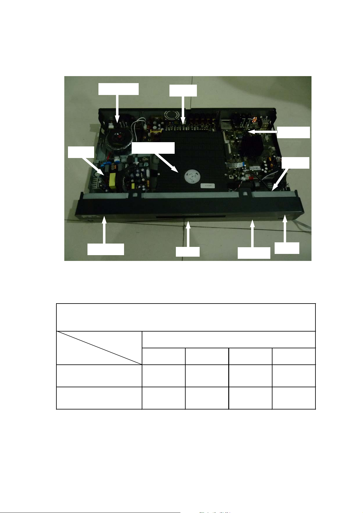
Technical Specification and Connection Facilities
1. Technical Specification and Connection Facilities
1.1 PCB Locations
Power Board
VFD Display Board
Power Socket Board
Bly-Ray Loader Driver
Output Board
LED Board
Touch Key Board
Decoder Board
WIFI Module
MCU Board
Specifications differences
Type/Versions
Specifications /12 /51 /93 /98
Voltage 230V 230V 110V-240V 110V-240V
Frequency 50Hz 50Hz 50Hz-60Hz 50Hz-60Hz
2-1
BDP9600
Page 4

Technical Specifications and Connection Facilities
1.2 General
Power supply : 110-240V, 50Hz~60Hz
Power consumption : 30W
Standby power consumption : <0.2 W
1.3 Connectivity
CD-DA(PCM)/VideoCD(MPEG-1)
Output Voltage : 2V ± 0.5dB
Signal to Noise Ratio
8QZHLJKWHG G%
$ZHLJKWHG G%
:LWK$XWRPXWH G%
2XWEDQG$WWHQXDWLRQ$ERYHN+]G%
DVD(LPCM / MPEG-2 /Dobly AC-3)
Output Voltage : 2V ± 0.5dB
6LJQDOWR1RLVH5DWLRG%
Outband Attenuation(Above25kHz) :
Digital Audio Outputs
LPCM : accordingIEC 60958-3
MPEG 1, MPEG 2, AC3 : according IEC 61937
DTS : according IEC 61937+
addendum
Coaxial & Optical output
2XWSXWVLJQDO$PSOLWXGHȍWHUPLQDWHU9SS
2XWSXWLPSHGDQFHȍ
DC Output voltageȍWHUPLQDWHU9
Video Supporting Format
Signal system : PAL/NTSC
HDMI output : 480p,576p,720p,1080i,
Video output : 480/576i,480/576p,
CVBS Output Component
Amplitude Output : 1000mVpp ± 10%
White Bar : 714mVpp ± 10%
Sync.Amplitude : 286mVpp ± 10%
S/N Luminunce G%
Chroma/Luminunce Delay(2T pulse) :
DC Level :
Video Output Component
Amplitude Output : 1000mVpp ± 10%
White Bar : 714mVpp ± 10%
Sync.Amplitude : 286mVpp ± 10%
S/N Luminunce G%
DC Level :
USB
Compatibility : USB2.0
Type of connector : Series A Connector
Class support : UMS(USB Mass Storage Class)
File System : FAT12,FAT16,FAT32
HDMI Output
Compatibility : HDMI Version 1.4
Type of connector : Type A Connector(19pins)
-50dB
1080p,1080p24
720p,1080i
20nS
1V
1V
1.4 Dimension and Weight
Set Dimension WxHxD : 435x70x260(mm)
Net Weight : 5.0kg
1.5 Laser Output Power & Wavelength
DVD
Output power : 6mW
Wavelength : 655 +10nm/-10nm
CD
Output power : 7mW
Wavelength : 790 +10nm/-20nm
1.6 Playability
Video Playback
1. Playback Media:
CD-R/CD-RW, DVD+R/+RW,
DVD-R/-RW, DVD-Video, Video
CD/SVCD, DVD+R DL, DVD-R
DL,USB flash drive
2. Compression Formats:
MPEG2, MPEG1, DivX 3.11, DivX
4.x, DivX 5.x, DivX 6.0, MPEG4
Audio Playback
1. Playback Media:
Audio CD, CD-R/RW, DVD+R DL,
DVD+R/+RW, DVD-R/-RW, MP3CD,MP3-DVD,USB flash drive,
WMA-CD
2. Compression Format:
Dolby Digital, MP3, MPEG2
Multichannel, PCM, WMA
3. MPEG1 bit rates: 64-384 kbps
and VBR
Still Picture Playback
1. Playback Media: CD-R/RW,
DVD+R DL, DVD+R/+RW, DVDR/-RW, Picture CD, USB Digital
Camera(PTP),USB flash drive
2. Picture Compression Format:
JPEG, JPEG digital camera
photos
3. Picture enhancement: Slideshow
with MP3 playback, Create
albums, Rotate, Slideshow with
music playback, Zoom
x
x
x
x
x
x
x
x
2-2
Page 5
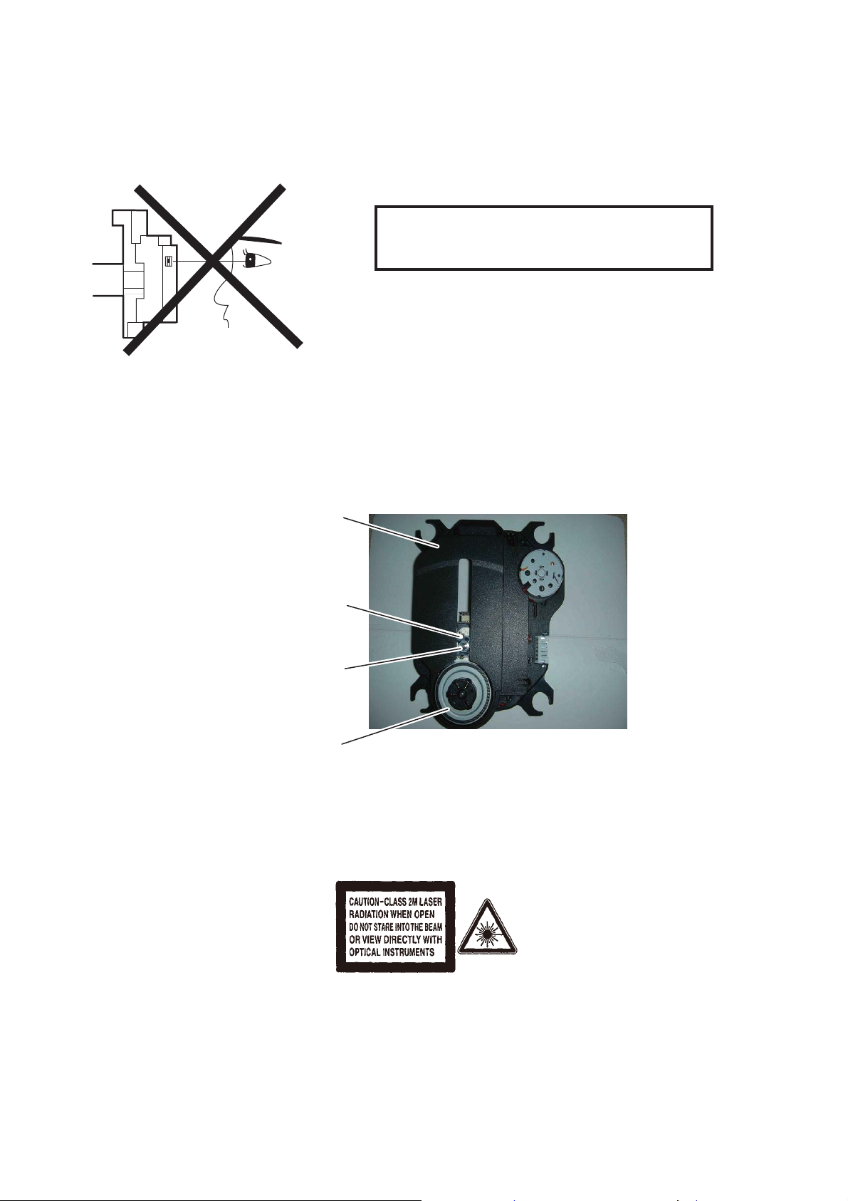
Laser Beam Safety Precautions
This Blu-Ray player uses a pickup that emits a laser beam.
Do not look directly at the laser beam coming
from the pickup or allow it to strike against your
skin.
The laser beam is emitted from the location shown in the figure. When checking the laser diode, be sure to keep
your eyes at least 30 cm away from the pickup lens when the diode is turned on. Do not look directly at the laser
beam.
CAUTION: Use of controls and adjustments, or doing procedures other than those specified herein, may result in
hazardous radiation exposure.
Drive Mechanism Assembly
Laser Beam Radiation
Laser Pickup
Turntable
Location: Inside Top of Blu-Ray mechanism.
3-1
Page 6

Important Safety Precautions
Important
Read and understand all instructions before you use
your home theater. If damage is caused by failure to
follow instructions, the warranty does not apply.
Safety
Riskof electricshockor re!
Neverexposetheproductand
accessories to rain or water. Never place
liquid containers, such as vases, near the
product. If liquids are spilt on or into the
product, disconnect it from the power
outlet immediately. Contact Philips
Consumer Care to have the product
checked before use.
Never place the product and accessories
near naked
including direct sunlight.
Neverinsertobjectsintotheventilation
slots
or other openings on the product.
Wherethemainsplugoranappliance
coupler is used as the disconnect device,
the disconnect device shall remain readily
operable.
Disconnect the product from the power
outlet before lightning storms.
Whenyoudisconnectthepowercord,
always pull the plug, never the cable.
Riskof short circuit or
Before you connect the product to the
poweroutlet,ensurethatthepower
voltage matches the value printed on the
back or bottom of the product. Never
connec
if the voltage is different.
Risk of injury or damage to the home theater!
For wall-mountable products, use only
the supplied wall mount bracket. Secure
the wall mount to a wall that can support
the combined weight of the product
and the wall mount. Koninklijke Philips
Electronics N.V. bears no responsibility
for improper wall mounting that results in
accident,injuryordamage.
ames or other heat sources,
re!
ttheproducttothepoweroutlet
For speakers with stands, use only the
supplied stands. Secure the stands to
the speakers tightly. Place the assembled
stands on
support the combined weight of the
speaker and stand.
Never place the product or any objects
on power cords or on other electrical
equipment.
If the product is transported in
temperatures below 5°C, unpack the
product and wait u
matches room temperature before
connecting it to the power outlet.
Visible and invisible laser radiation when
open. Avoid exposure to beam.
Do not touch the disc optical lens inside
the disc compartment.
Risk of overheating!
Never install this product in a con
space. Always leave a space of at least
four inches around the product for
ventilation. Ensure curtains or other
objects never cover the ventilation slots
on the product.
Risk of contamination!
Do not mix batteries (old and new or
carbon and alkaline,
Remove batteries if they are exhausted
oriftheremotecontrolisnottobeused
for a long time.
Batteries contain chemical substances,
they should be disposed of properly.
t,levelsurfacesthatcan
ntil its temperature
etc.).
Product care
Do not insert any objects other than discs
into the disc compartment.
Donotinsertwarpedorcrackeddiscs
intothedisccompartme
Remove discs from the disc compartment
ifyouarenotusingtheproductforan
extended period of time.
Only use microfiber cloth to clean the
product.
nt.
ned
4-1
Page 7

Important Safety Precautions
Disposal of your old product and
batteries
Your product is designed and manufactured
with high quality materials and components,
which can be recycled and reused.
When this crossed-out wheeled bin symbol
is attached to a product it means that the
product is covered by the European Directive
2002/96/EC.Pleaseinformyourselfaboutthe
local separate collection system for electrical
and electronic products.
Please act according to your local rules and
do not dispose of your old products with your
normal household waste.
Corr
ect disposal of your old product helps to
prevent pote
the environment and human health.
ntial negative consequences for
Your product contains batteries covered by
the European Directive 2006/66/EC, which
cannot be disposed with normal household
waste.
Please inform yourself about the local rules
on separate collection of batteries because
correct disposal helps to prevent negative
consequences for the environmental and
human health.
4-2
Page 8
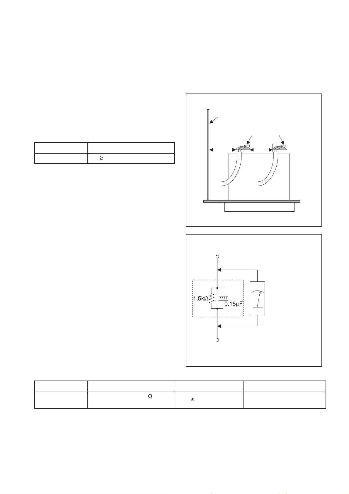
Safety Check after Servicing
Examine the area surrounding the repaired location for damage or deterioration. Observe that screws, parts, and
wires have been returned to their original positions. Afterwards, do the following tests and confirm the specified
values to verify compliance with safety standards.
1. Clearance Distance
When replacing primary circuit components, confirm
specified clearance distance (d) and (d’) between
soldered terminals, and between term
surrounding metallic parts. (See Fig. 1)
Table 1: Rating
s for selected area
inals and
Chassis or Secondary Conductor
Primary Circuit
AC Line Voltage Clearance Distance (d), (d
110V~220V
Note: This table is unofficial and for reference only. Be
sure to confirm the precise values.
3.2 mm (0.126 inches)
’)
2. Leakage Current Test
Confirm the specified (or lower) leakage current
between B (earth ground, power cord plug prongs) and
externally exposed accessible parts (RF terminals,
antenna terminals, video and audio input and output
terminals, microphone jacks, earphone jacks, etc.) is
than or equal to the specified value in the table
lower
below.
Measuring Method (Power ON):
Insert load Z between B (earth ground, power cord plug
prongs) and exposed accessible parts. Use an AC
voltmeter to measure across the terminals of load Z.
See Fig. 2 and the following table.
d' d
Fig. 1
Exposed Accessible Part
Z
AC Voltmeter
(High Impedance)
Earth Ground
B
Power Cord Plug Prongs
Table 2: Leakage current ratings for selected areas
AC Line Voltage Load Z Leakage Current (i) Earth Ground (B) to:
110V~220V
Note: This table is unofficial and for reference only. Be sure to confirm the precise values.
0.15 μF CAP. & 1.5 k
Connected in parallel
RES.
i
0.5 mA Peak Exposed accessible parts
5-1
Fig. 2
Page 9
Safety Information, General Notes & Lead Free Requirements
1 Safety Instructions
1.1 General Safety
Safety regulations require that during a repair:
Connect the unit to the mains via an isolation transformer.
Replace safety components, indicated by the symbol
only by components identical to the original ones. Any
other component substitution (other than original type)
Safety regulations require that after a repair, you must return
the unit in its original condition. Pay, in particular, attention to
the following points:
Route the wires/cables correctly
mounted cable clamps.
damage.
Check the electrical DC resistance between the mains
plug and the secondary side:
1. Unplug the mains cord, and connect a wire between
the two pins of the mains plug.
2. Set the mains switch to the ‘on’ position (keep the
mains cord unplugged!).
3. Measure the resistance value between the mains
plug and the front panel, controls, and chassis
bottom.
4. Repair or correct unit when the resistance
5. Verify this, before you return the unit to the customer/
user (ref. UL-standard no. 1492).
6. Switch the unit ‘off’, and remove the wire between the
two pins of the mains plug.
1.2 Laser Safety
This unit employs a laser
may remove the cover, or attempt to service this device (due
to possible eye injury).
2 Warnings
2.1 General
All ICs and many other semiconductors are susceptible to
electrostatic discharges (ESD,
,
during repair can reduce life drastically. Make sure that,
during repair, you are at the same potential as the mass
of the set by a wristband with resistance. Keep
components and tools at this same potential.
Available ESD protection equipment:
– Complete kit ESD3 (small tablemat, wristband,
4822 310 10671.
– Wristband tester 4822 344 13999.
Be careful during measurements in the live voltage
section. The primary side of the power supply, including
the heatsink, carries live mains voltage when you
connect the player to the mains (even when the
player is ‘off’!). It is possible to touch copper tracks and/
or components in this unshielded primary area, when
you service the player. Service personnel must take
precautions to prevent touching this area or components
in this area. A ‘lightning stroke’ and a stripe-marked
printing on the printed wiring board, indicate the primary
side of the power supply.
Never replace modules, or components, while the unit is
‘on’.
2.2 Laser
The use of optical instruments with this product, will
Only quali ed service personnel may remove the cover or
attempt to service this device, due to possible eye injury.
Repair handling should take place as much as possible
with a disc loaded inside the player.
T
shield:
). Careless handling
Laser Device Unit
epyT
:AIGalnN(BD)
:AIGalnP(DVD)
: AIGalnP(CD)
Wavelength : 650 nm (DVD)
)DC/DCV(mn087:
405nm(BD):
Output Power : 20 mW
)gnitirwWR+DVD(
Wm8.0:
)gnidaerDVD(
Wm3.0:
)gnidaerDC/DCV(
Beam divergence : 60 degree
CLASS 1
LASER PRODUCT
1-2erugiF
Note: Use of controls or adjustments or performance of
procedure other than those speci
ed herein, may result in
A
CAUTION VISIBLE AND INVISIBLE LASER RADIATION WHEN OPENAVOID EXPOSURE TO BEAM
ADVARSEL SYNLIG OG USYNLIG LASERSTRÅLING VED ÅBNING UNDGÅ UDSÆTTELSE FOR STRÅLING
ADVARSEL SYNLIG OG USYNLIG LASERSTRÅLING NÅR DEKSEL ÅPNES UNNGÅ EKSPONERING FOR STRÅLEN
VARNING SYNLIG OCH OSYNLIG LASERSTRÅLNING NÄR DENNA DEL ÄR ÖPPNAD BETRAKTA EJ STRÅLEN
VARO ! AVAT TAESSA OLETALTTIINA NÄKYVÄLLE JA NÄKYMÄTTÖMÄLLE LASER SÄTEILYLLE. ÄLÄ KATSO SÄTEESEEN
VORSICHT SICHTBARE UND UNSICHTBARE LASERSTRAHLUNG WENN ABDECKUNG GEÖFFNETNICHT DEM STRAHL AUSSETSEN
DANGER VISIBLE AND INVISIBLE LASER RADIATION WHEN OPENAVOID DIRECT EXPOSURE TO BEAM
ATTENTION RAYONNEMENT LASER VISIBLE ET INVISIBLE EN CAS D’OUVERTURE EXPOSITION DANGEREUSE AU FAISCEAU
Figure 2-2
6-1
Page 10
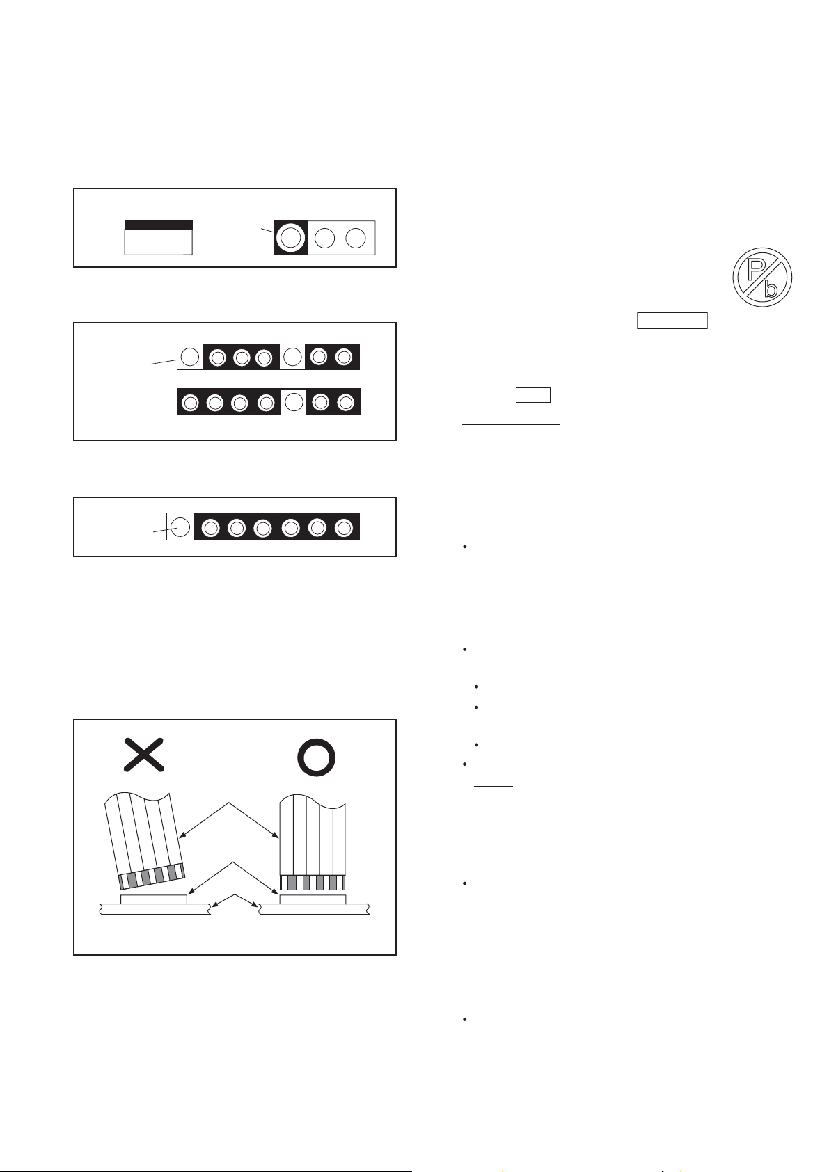
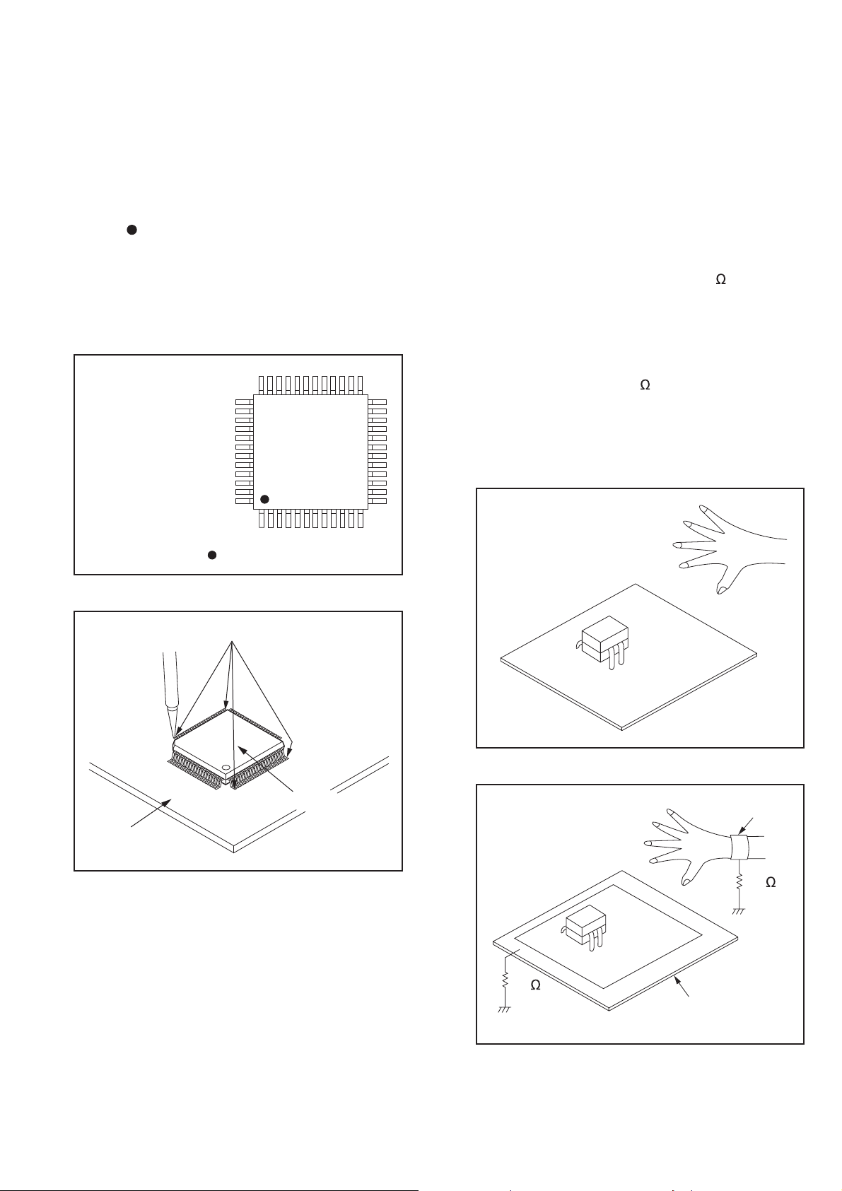
Standard Notes for Servicing, Lead Free Requirements & Handling Flat Pack IC
Circuit Board Indications
1. The output pin of the 3 pin Regulator ICs is
indicated as shown.
Top View
Out
2. For other ICs, pin 1 and every fifth pin are
indicated as shown.
Pin 1
3. The 1st pin of every male connector is indicated as
shown.
Pin 1
Input
In
Bottom View
5
10
Instructions for Connectors
1. When you connect or disconnect the FFC (Flexible
Foil Connector) cable, be sure to first disconnect
the AC cord.
2. FFC (Flexible Foil Connector) cable should be
inserted parallel into the connector, not at an
angle.
FFC Cable
Connector
CBA
* Be careful to avoid a short circuit.
Pb (Lead) Free Solder
When soldering, be sure to use the Pb free solder.
Information about lead-free soldering
Philips CE is producing lead-free sets from 1.1.2005
onwards.
IDENTIFICATION
Regardless of special logo (not always
indicated)
One must treat all sets from
onwards, according to the next rule:
Serial Number gives a 14-digit. Digit 5&6 shows the
YEAR, and digit 7&8 shows the WEEK.
So from onwards=from 1 Jan 2005 onwards
0501
Important note : In fact also products of year 2004
must be treated in this way as long as you avoid
mixing solder-alloys (leaded/ lead-free). So best to
always use SAC305 and the higher temperatures
belong to this.
Due to lead-free technology some rules have to be
respected by the workshop during a repair:
Use only lead-free solder alloy Philips SAC305 with
order code 0622 149 00106. If lead-free solderpaste is required, please contact the manufacturer
of your sol
paste within workshops should be avoided because
paste is not easy to store and to handle.
Use only adequate solder tools applicable for leadfree solder alloy. The solder tool must be able
To reach at least a solder-temperature of 400°C,
To stabilize the adjusted temperature at the solder-
tip
To exchange solder-tips for different applications.
Adjust your solder tool so that a temperature around
360°C
solder joint. Heating-time of the solder-joint should
not exceed ~ 4 sec. Avoid temperatures above
400°C otherwise wear-out of tips will rise drastically
and flux-fluid will be destroyed. To avoid wear-out of
tips switch off un-used equipment, or reduce heat.
Mix of lead-free solder alloy / parts with leaded
solder alloy / parts is possible but PHILIPS
recommends strongly to avoid mixed solder alloy
types (leaded
If one cannot avoid or does not know whether
product is lead-free, clean carefully the solder-joint
from old solder alloy and re-solder with new solder
alloy (SAC305).
Use only original spare-parts listed in the ServiceManuals. Not listed standard-material (commodities)
has to be purchased at external companies.
der-equipment. In general use of solder-
- 380°C is reached and stabilized at the
and lead-free).
1 Jan 2005
7-1
Page 11
Standard Notes for Servicing, Lead Free Requirements & Handling Flat Pack IC
Special information for BGA-ICs:
- always use the 12nc-recognizable soldering
temperature profile of the specific BGA (for desoldering always use the lead-free temperature
profile, in case of doubt)
- lead free BGA-ICs will be delivered in so-called
'dry-packaging' (sealed pack including a silica gel
pack) to protect the IC against moisture. After
opening, dependent of MSL-level seen on indicatorlabel in the bag, the BGA-IC possibly still has to be
baked dry. (MSL=Moisture Sensit
will be communicated via AYS-website.
Do not re-use BGAs at all.
For sets produced before 1.1.2005 (except products
of 2004), containing leaded solder-alloy and
components, all needed spare-parts will be available
till the end of the service-period. For repair of such
sets nothing changes.
On our website
www.atyourservice.ce.Philips.com
information to:
BGA-de-/soldering (+ baking instructions)
Heating-profiles of BGAs and other ICs used in
Philips-sets
You will find this and more technical information within
the “magazine”, chapter “workshop news”.
For additional questions please contact your local
repair-helpdesk.
ivity Level). This
you find more
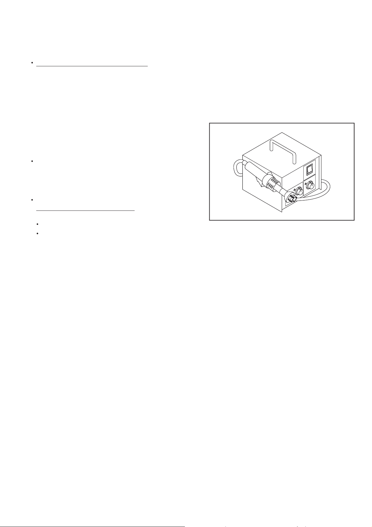
How to Remove / Install Flat Pack-IC
1. Removal
With Hot-Air Flat Pack-IC Desoldering Machine:
1. Prepare the hot-air flat pack-IC desoldering
machine, then apply hot air to the Flat Pack-IC
(about 5 to 6 seconds). (Fig. S-1-1)
Fig. S-1-1
2. Remove the flat pack-IC with tweezers while
applying the hot air.
3. Bottom of the flat pack-IC is fixed with glue
CBA; when removing entire flat pack-IC, first apply
soldering iron to center of the flat pack-IC and heat
up. Then remove (glue will be melted). (Fig. S-1-6)
4. Release the flat pack-IC from the CBA using
tweezers. (Fig. S-1-6)
to the
CAUTION:
1. The Flat Pack-IC shape may differ by models. Use
an appr
machine, whose shape matches that of the Flat
Pack-IC.
2. Do not supply hot air to the chip parts around the
flat pack-IC for over 6 seconds because damage
to the chip parts may occur. Put masking tape
around the flat pack-IC to protect other parts from
damage. (Fig. S-1-2)
opriate hot-air flat pack-IC desoldering
7-2
Page 12
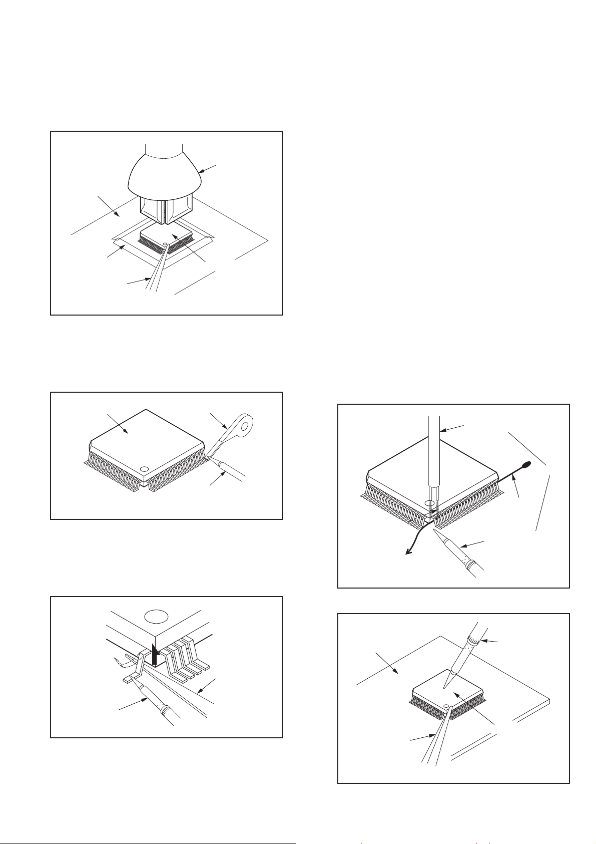
Standard Notes for Servicing, Lead Free Requirements & Handling Flat Pack IC
3. The flat pack-IC on the CBA is affixed with glue, so
be careful not to break or damage the foil of each
pin or the solder lands under the IC when
removing it.
Hot-air
Flat Pack-IC
Desoldering
CBA
Masking
Tape
Tweezers
With Soldering Iron:
1. Using desoldering braid, remove the solder from
all pins of the flat pack-IC. When you use solder
flux which is applied to all pins of the flat pack-IC,
you can remove it easily. (Fig. S-1-3)
Flat Pack-IC
Desoldering Braid
Machine
Flat Pack-IC
Fig. S-1-2
4. Release the flat pack-IC from the CBA using
tweezers. (Fig. S-1-6)
With Iron Wire:
1. Using desoldering braid, remove
all pins of the flat pack-IC. When you use solder
flux which is applied to all pins of the flat pack-IC,
you can remove it easily. (Fig. S-1-3)
2. Affix the wire to a workbench or s
point, as shown in Fig. S-1-5.
3. While heating the pins using a fine tip soldering
iron or hot air blower, pull up the wire as the solder
melts so as to lift the IC leads from the CBA
contact pads as shown in Fig. S-1-5.
4. Bottom of the
CBA; when removing entire flat pack-IC, first apply
soldering iron to center of the flat pack-IC and heat
up. Then remove (glue will be melted). (Fig. S-1-6)
5. Release the flat pack-IC from the CBA using
tweezers. (Fig. S-1-6)
Note: When using a soldering iron, care must be
taken to
being held by glue. When the flat pack-IC is
removed from the CBA, handle it gently
because it may be dama
flat pack-IC is fixed with glue to the
ensure that the flat pack-IC is not
the solder from
olid mounting
ged if force is applied.
Soldering Iron
Fig. S-1-3
2. Lift each lead of the flat pack-IC upward one by
one, using a sharp pin or wire to whic
not adhere (iron wire). When heating the pins, use
a fine tip soldering iron or a hot air de
machine. (Fig. S-1-4)
Fine Tip
Soldering Iron
3. Bottom of the flat pack-IC is fixed with glue to the
CBA; when removing entire flat pack-IC, first apply
soldering iron to center of the flat pack-IC and heat
up. Then remove (glue will be melted). (Fig. S-1-6)
h solder will
soldering
Sharp
Pin
Fig. S-1-4
7-3
To Solid
Mounting Point
CBA
Tweezers
Hot Air Blower
or
Iron Wire
Soldering Iron
Fig. S-1-5
Fine Tip
Soldering Iron
Flat Pack-IC
Fig. S-1-6
Page 13
Standard Notes for Servicing, Lead Free Requirements & Handling Flat Pack IC
2. Installation
1. Using desoldering braid, remove the solder from
the foil of each pin of the flat pack-IC on the CBA
so you can install a replacement flat pack-IC more
easily.
2. The “
(See Fig. S-1-7.) Be sure this mark matches the 1
on the PCB when positioning for installation. Then
presolder the four corners of the flat pack-IC. (See
Fig. S-1-8.)
3. Solder all pins of the flat pack-IC. Be sure that
none of the pins have solder bridges.
” mark on the flat pack-IC indicates pin 1.
Example :
Pin 1 of the Flat Pack-IC
is indicated by a " " mark.
Fig. S-1-7
Instructions for Handling Semiconductors
Electrostatic breakdown of the semi-conductors may
occur due to a potential difference caused by
electrostatic charge during unpacking or repair work.
1. Ground for Human Body
Be sure to wear a grounding band (1 M ) that is
properly grounded to remove any static electricity that
may be charged on the body.
2. Ground for Workbench
Be sure to place a conductive sheet or copper plate
with proper grounding (1 M
other surface, where the semi-conductors are to be
placed. Because the static electricity charge on
clothing will not escape through the body grounding
band, be
with your clothing.
careful to avoid contacting semi-conductors
<Incorrect>
) on the workbench or
CBA
Presolder
Flat Pack-IC
Fig. S-1-8
<Correct>
1M
CBA
Grounding Band
1M
CBA
Conductive Sheet or
Copper Plate
7-4
Page 14
Direction of Use
j
*The following excerpt of the DFU/QSG serves as an introduction to the set.
The Complete Direction for Use can be download in different languages from
the internet site of Philips Customer care Center : www.support.philips.com
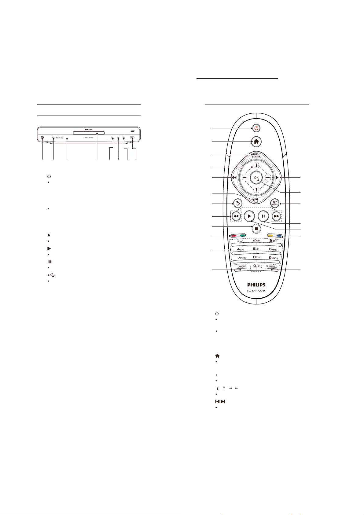
Product overview
Main unit
c
b
a
a
bDisplaypanel
cIRsensor
d Disc compartment
e
f
g
h
Turn on this player or switch to standby
mode.
Detect signals from the remote control.
Always point the remote control at the
IR sensor.
Open or close the disc compartment .
Startorresumeplay.
Pause play.
jack
Connect a USB device.
Remote control
a
b
c
g
e
d
h
f
d
e
f
g
e
q
p
h
i
o
n
j
k
l m
a
b
cDISC/POP-UP
d
e
Turn on this player or switch to standby
mode.
When EasyLink is enabled, press and
hold for at least three seconds to turn all
connected HDMI CEC compliant devices
to standby.
Accessthehomemenuofthisplayer.
BD:Accessorexitthepop-upmenu.
DVD: Access or exit the disc menu.
/ / /
Navigate through the menus.
/
Skip to the previous or next title, chapter,
or track.
8-1
Page 15

Direction of Use
Remote Control
f
g
h
i
j Color buttons
k Alphanumeric buttons
lAUDIO
m SUBTITLE
n
o
pTOPMENU
qOK
Access options for the current activity or
selection.
Return to a previous display menu.
/
Search backward or forward.
Stop play.
Press and hold to open/close the disc
compartment.
BD: Select tasks or options.
Selectanitemtoplay.
Enter values.
Enter letters via SMS style entry.
Select an audio language or channel on
adisc.
Select a subtitle language on a disc.
Start or resume play.
Pause play.
Move the paused picture forward frame
by frame .
BD: Display the top menu.
DVD: Display the title menu.
rm an entry or selection.
Con
3 Connect
Make the following connections to use this player.
Basic connections:
Video
Audio
Power
Optional connections:
Route audio to other devices
HDMI-compliant AV receiver/ampli er
Multi-channel AV ampli er/receiver
DigitalAVampli er/receiver
Analog stereo system
USB device
Wired/Wireless network
Note
Refer to the type plate at the back or bottom of the
product for identi cation and supply ratings.
Before you make or change any connections, ensure that
all the devices are disconnected from the power outlet.
Connect video/audio cables
Select the best video connection that theTV can support.
Option 1:Connect to the HDMI jack (for a
HDMI, DVI or HDCP-compliant TV).
Option 2:Connect to the component video
jacks (for a standard TV or Progressive Scan TV).
Option 3:Connect to the composite video
jack (for a standard TV).
Option 1: Connect to the HDMI jack
8-2
HDMI IN
Connect an HDMI cable (not supplied) to:
1
the
HDMI jack on this player.
the HDMI input jack on the TV.
Page 16

Direction of Use
Tip
If the TV has a DVI connector only, connect via an
HDMI/DVI adaptor. Connect an audio cable for sound
output.
If there is a blank TV screen under HDMI connection,
ontheremotecontrolpress and then press “731”
(numeric buttons) to recover picture display.
If this player connects to a TV compatible with 1080p
or 1080p/24Hz, Philips recommends HDMI category 2
cable, also known as High Speed HDMI cable, for optimal
video and audio output.
To play the digital video images of a BD-video or DVDvideo via anHDMI connection, it is necessary that both this
player and the display device(or an AV receiver/ampl
support a copyright protection system called HDCP (highbandwidth digital content protection system).
This connection provides the best picture quality.
Option 2: Connect to the component
video jacks
Y
Pb
Pr
AUDIO IN
Option 3: Connect to the composite
video jack
AUDIO IN
VIDEO IN
er)
1
Connect a composite video cable (not
supplied) to:
the
VIDEOjack on this player.
the VIDEO input jack on the TV.
2 Connect the audio cables (not supplied) to:
the
Audio LINE OUT- L/Rjacks on this
player.
the AUDIO input jacks on the TV.
Tip
ThevideoinputjackontheTVmightbelabeledasA/V
IN, VIDEO IN, COMPOSITE or BASEBAND.
1
Connect the component video cables (not
supplied) to:
the
Y Pb/Cb Pr/Crjacks on this player.
the COMPONENT VIDEO input jacks
on the TV.
2 Connect the audio cables (not supplied) to:
the
Audio LINE OUT-L/Rjacks on this
player.
the AUDIO input jacks on the TV.
Tip
The component video input jack on the TV might be
labeled as Y Pb Pr or YUV.
Route audio to other devices
You can route the audio from this player to other
devices.
Connect to an HDMI-compliant AV
receiv
HDMI IN
1 Connect an HDMI cable (not supplied) to:
the
HDMI jack on this player.
the HDMI jack input jack on the device.
8-3
Page 17

Direction of Use
Tip
The HDMI connection provides the best audio quality.
Connect to a multi-channel AV receiver/
7.1 CH AUD IO INP UT
1 Connect a coaxial cable (not supplied) to:
COAXIAL jack on this player.
the
the COAXIAL/DIGITAL input jack on
the device.
Connect to optical jack
OPTICAL
1 Connect an optical cable (not supplied) to:
the
OPTICALjackonthisplayer.
the OPTICAL/DIGITAL input jack on the
device.
Connect an analogue stereo system
AV IN
1 Connect the 7.1-channel audio cables (not
supplied) to:
7.1 CH AUDI O OUTPUT
the
jacks on
this player.
the corresponding AUDIO input jacks
on the device.
Tip
To connect 5.1-channel AV receiver/ampli er, connect
the 7.1-channel audio jacks except theSL/SR jacks.
You can optimize the speaker output (see “Adjust
settings” >[Audio]>[Speaker Setup]).
Connect to a digital A receiver
Connect to coaxial jack
COAXIAL
1
Connect the audio cables (not supplied) to:
Audio LINE OUT-L/R jacks on this
the
player.
the AUDIO input jacks on the device.
Connect a USB device
1 Connect a USB device to the
on the front panel of this player.
Note
Press , and select [Browse USB] in the menu
to access the content and play the
Connect a USB device only to the
this player.
Philips does not guarantee compatibility with all
USB devices.
les.
jack on
(USB) jack
8-4
Page 18

Connect a network
With a wired or wireless connection (see “Get
started” > “Set up a network”), you can connect
this player to:
theInternet(forsoftwareupdate/BD
Live/Net TV service).
or a home network (to access media
from a DLNA media server, e.g. PC).
Note
Internet access to Philips website for software update
maynotbeallowed,dependingontherouteryouuse
or the Internet Service Provider’s policy. Contact your
Internet Service Provider for more information.
Connect power
Caution
Riskofplayerdamage!Ensurethatthepowersupply
voltage corresponds to the voltage printed on the back
of the unit.
Before connecting the AC power cord, ensure you have
completed all other connections.
Direction of Use
es
Note
The type plate is located on the back of the player.
1 Connect the AC power cable to:
this player.
thewallsocket.
This player is ready to be set up for use.»
8-5
Page 19

Cabinet Disassembly Instructions
1. Disassembly Flowchart
This flowchart indicates the disassembly steps to gain
access to item(s) to be serviced. When reassembling,
follow the steps in reverse order. Bend, route, and
dress the cables as they were originally.
[1] Aluminum decorative floor,
Machine bracket
[2] TOP Cover
[3] Machine shield
[4] DVDDoor
[5] Bly-Ray Driver
[6] Top Loader Driver
[7] Transformer
[8] Power socket board,
Decoder board,
output board,Power
board
[9] USB Terminal board
Note:
(1) Identification (location) No. of parts in the figures
(2) Name of the part
(3) Figure Number for reference
(4) Identification of parts to be removed, unhooked,
unlocked, released, unplugged, unclamped, or
desoldered.
0x = Screw, CNxx/Jxx/CONxx = Connector
D3.5X12BA is specification of screw.
* = Unhook, Unlock, Release, Unplu
g, or Desolder
e.g. 7(01) = seven Screws
[10] Front panel
[11]Touch Key Board
VFD Display Board
[12] Transparent PMMA,Tou -
ch pad,Power button spport,LED lens
[13] USB door,Decorative Lenses,
Touch pad
2. Disassembly Method
ID/
Loc.
No.
[1]
[2]
[3]
[4]
[4]
Part
Aluminum decorative floor, Machine bracket
Machine shield
Bly-Ray Loader
Driver
Top Loader Cover
Transformer
Fig.
No.
4(01) D3x6BMTT
D1
D3
3(02) D3x8BT
4(03) D3x8BT
D5
D6
2(08) D3x5BMTT
1(04) D4x6KMTT,4x6KT
D7
Removal
Remove/*Unhook/
Unlock/Release/
Unplug/Desolder
01
Fig. D1
Note
Fig. D2
Power socket bo-
ard, Decoder boa-
[5]
rd, Output board
Power board
Touch Key board
[6]
VFD display board
7(06) D3x4BMTT
D8
18(05) D3x8BT
D11
10(07) D2.6x8BT
9-1
Page 20

Cabinet Disassembly Instructions
Fig. D3
02
08
Fig.D6
04
Fig. D4
Fig. D5
03
Fig. D7
06
05
05
05
Fig. D8
9-2
Page 21

Fig. D9
Cabinet Disassembly Instructions
Fig. D12
Fig. D10
Fig. D11
Fig. D13
07
9-3
Page 22

Troubleshooting
No power
Check the Power Cord
is connected
Y
Check whether the
Power Transfer Board has
provided voltage output—
(AC220V)
Y
Check the FUSE is ok or
not?
Y
Check whether the
PowerBoard has provided
voltage output
Y
Check the FUSE is ok or
not?
Replace a new
N
Power Transfer
Board
Replace a new
N
one
Replace a new
N
Board
Replace a new
N
one
No sound
Y
Adjust the volume
Y
Check the connect cable is
OK or NOT
Y
Check whether provide 18V
voltage for Digital Output
Board jack(J3)
Y
Check Digital output board(J2)
& decoder board(xp8)between
the flat connect wire is OK or
NOT and Re-planted
Y
Test the decoder board jack(xp8)
pin no.22#(+12vA)、23#(-12V)
has provided voltage
Y
Confirm decoder board jack(xp8)
location pin no.16#(mute) low level
N
Replace a
N
new one
Check&replace
the transformer
Replace a
N
new one
Check&replace the
N
digital output board
Check related MUTE
N
circuit decoder board
Can’t Loading
Y
Confirmed machine
tray in and out
action normal
Confirmed the disc piece
revolving movement is
whether normal
Y
Check the flat connect wire is
OK or NOT and Re-planted
Check&replace the Loader
N
Y
Y
check decoder board
location XP4 jack pin
no.3#~4# has 3.6v provide voltage
Test decoder board jack
(XP4)pin no.1#~2# impedance 0ohm
N
Test decoder board jack
(XP3) W\U\V between
wheter has12V provide
voltage
Replace a
N
new one
No display
Check the power pcb “CON1”
connection to display board
cable normal
Y
Check location CON1 in power
board has normal voltage:+5v、
-27v、VF(-12V)、S5V(5V)、
and has STB provide voltage
Y
Check location U201 in display
board pin No15#、37# has 5V
provide voltage,check 27# pin
has -30v provide voltage
Y
Use Oscillograph to checkVFD
data cable if has normal nignal or
not ,the check location is U201 pin
No 5#(VFD DATA)、8#(CLK)and
STB provide voltage
Y
replace display board IC
U201
N
Re- insert
N
replace the
power board
N
check&replace the
N
decoder board
No picture on HDMI connection
Check if the HDMI cable
is usable
Y
Check a television
change to HDMI mode
Y
Use Oscillograph to check jack
(J300)pin No 15#(HDMI_SCL)、
16#(HDM_SDA)wave if normal
check J300 cable pin No 1#、
3#、4#、6#、7#、9#、10# TX
signal normal or no
Y
Check &replaec the J300
jack
Replace a new
N
HDMI cable
Change to HD-
N
MI mode
N
Replace the
decoder board
Y
use oscillograph to check decoder
board jack(xp8)pin no.6#(MCLK)、
8#(BCK)data whether normal
Y
replace digital output board
N
replace decoder board
10-1 10-1
Page 23

Software Upgrading Procedure
1. Download the Software from Philips support
Website:
http://www.philips.com/support.
2. Copy the Software upgrade file into USB device.
A. Connect to TV and Turn on Main Unit,
Select Upgrad from USB,TV Screen Display:
Press OK on Remote Control,
TV Screen Display:
C. Software Upgrading
D. When Software Upgrading finish,TV screen
display
B. Press OK on Remote Control,
TV Screen Display:
Software Upgrade finish.
11-1
Page 24

Software Version Check
1. Select the “ ”, like below show:
2. TV Screen Display,select Version Info.
4.Press “ ” on Remote Control:
VFD display:
3. Select OK to get the Version information :
5. Press 8-5-2-0 on Remote Control,can find
Software Version:
11-2
Page 25

Repair Service Flow
How to replace the defective Blu-ray Loader
1.Remove the defective Blu-ray Loader.
2.Remove the shield cover at the top of Blu-ray Loader as shown below:
3.Assembly Blu-ray Loader to “HA1,HA2,HA3” on the top of BD Board as shown below:
4. Remove soldered joint on the ESD protection points.
The ESD protection
points on the top of board.
The ESD protection points
on the bottom of board.
Top Side
Bottom Side
HA3
HA1
HA2
Note:The ESD protection points on any one side must be soldered if
a.The Blu-ray Loader needs to be disconnected from connector HA1,HA2 and HA3 of
the BD Board.
b.The defective Blu-ray Loader is needed to be send back to supplier for failure analysis and
to support backcharging evidence.
12-1
Page 26

Repair Service Flow
BD board and Blu-ray Loader OPU matching procedure
Step1
1.Assemble loader to 8530 PCB
2.Remove laser protection point
3.Power on,Press“ ”<Home> button and input 85177 on R/C
4.Select item[5],then press<OK>,as shown below:
Step2
Insert USB device of MSC type and press<OK>button
on R/C as shown below:
12-3
Page 27

Repair Service Flow
Step3
Using Navigate buttons on R/C input the 6 digit @ Sanyo OPU
Input 1D info from left to right
Press<OK> button to save
Sanyo
12-4
Page 28

Repair Service Flow
Step4
Goto to Top manual and select
item[6]laser check press <OK>,as shown below:
Step5
Wait laser check pass to verify the
status of the assemble.
12-5
Page 29

Block Diagram
FAN
TRV412VH5
BD ROM ASA
UVWCOM
A+A-B+B-
WIFI DONGLE MODULE
VFD Display
KEY
SD(VOD)
USB
IR
UVWCOM
A+A-B+B-
WIFI DONGLE
VFD Driver
PT16312
IR
MCU
R5F21266
Display
MCU5V
IIC_MCU
CEC
AABBUVWC
LOAD+-
TRAY IN/OUT
Collimator II
TPC1391G4
Motor Driver
R2A30209SP
Ethernet
Ethernet
SMSC8710
WIFI DONGLE
VFD_BUS
DDR2
256M
SD_BUS
USB
IR
IIC_MCU
QDEO
Scalar
Kyoto 2750
IIC_QDEO
MPEG
MT8530KEFG
(Divx PlusHD)
Digital video out
Digital video in
NAND-FLASH
16G
DDRII
DDRII
DDRII
DDRII
HDMI_OUT
CEC
1G
1G
1G
1G
Buffer
FMS6363CS
ESD
REJECTOR
FAN
IIS_BUS
S/Pdif
CVBS
YUV
CEC
OPTION
OPTICAL
COAXIAL
CVBS
YUV
HDMI
12V
-12V
MPEG5V
Loader
SC5V
MPEG
Display
MCU5V
Transformer2
Transformer1
DAC
PCM1789
DAC
PCM1754
DAC
PCM1754
DAC
PCM1754
DAC
PCM1754
OP
OP
OP
OP
OP
POW318A
Regulator
4558
4558
4558
4558
4558
12V
7.1CH Audio OUT
12V
Regulator
7812
Regulator
OPTION
REL?
1 5
2
RELAY2
AC
2CHLt/Rt
-12V
Regulator
7912
4
3
Touched key
WT5700
Touch key x N
13-1 13-1
Page 30

Wiring Diagram
VFD DISPLAY BOARD
LED+
LED-
LED BOARD
GND
CLK
STB
ECO_POWER
GND
A5V
K0K1K2
MCU5V
DATA
KEY_STBY
LED_STBY
GND
GND
ANT1
K3
GND
IR
-30V
VF1
VF2
MCU5V
ECO_POWER
GND
~220V
~0V
POWER BOARD
Cable Location
No.:C103
AC220
0
AC220
D12V
+5V
+5V
GND
GND
+12V
GND
-12V
POWER SOCKET BOARD
AC21
0
AC21
D5V
GND
No.:ACC2
Cable Location
AC INPUT 100--240V/50-60HZ
POWER LINE
OUTPUT BOARD
Cable Location
No.:C102
Cable Location
No.:C100
GND
CLK
3.3V
GND
DATA
TOUCH KEY BOARD
MCU BOARD
GND
GND
D+
STB
CLK
HDMI5V
GND
MUTE
RST
CEC
SDA
SCL
14-1
LOAD+
LOADGND
TRAY+
TRAY-
VCC
D-
VCC2
D-2
D+2
GND
WIFI MODULE
HPD
DATA
GND
IR
ANT2
Cable Location
No.:C101
A+
A-B+B-
VWCDM
U
DECODER BOARD
Cable Location
NO.:W01
GND
I/O
D-12V
ADLRCK
A_MUTE
GND
GND
ADSDATA3
ADMCLK
ADSDATA4
GND
NC
GND
SDA
SCL
ADSDATA0
ACBCK
ADSDATA2
ADSDATA1
GND
GND
VCC5VNCD+12V
14-1
Page 31

Touch Key Board -- Circuit and Layout Diagram
K1
OPEN/CLOSE
K2
PLAY
K3
PAUSE
KEY1
KEY2
KEY3
C801
NC/5P
C802
NC/5P
C803
NC/5P
J801
1.0/5P
TKEY+3.3V
R801
2M
5
4
3
2
1
C804
104
TKEY+3.3V
GND
KEY_CLK
GND
KEY_DATA
C805
103
1
VDD
2
SI[0]
3
SI[1]
4
SI[3]
5
SI[8]
6
SI[10]
7
SI[11]
VSS8OUT11
IC-WT5700-S160
U801
OUT0
OUT1
OUT3
SCL
SDA
OUT8
OUT10
TKEY+3.3V
16
15
14
13
12
11
10
C806
9
10P
C807
10P
R802
R803
470
470
R804
10K
R805
47K
KEY_CLK
KEY_DATA
15-1 15-1
Page 32

Output Board -- Circuit Diagram
AOBCK
AOSDATA0
AOLRCK
A5V
L1 FB
+
CE3
CD11X/22UF16V/D4H7
A
AOBCK
AOSDATA1
AOLRCK
A5V
L3 FB
CE15
CD11X/22UF16V/D4H7
MUTE_0
+3.3VVDDA
R137 4.7R
+
CE59
CD11X/22UF16V/D4H7
L11 FB
L8 FB
L9 FB
L10 FB
A
AV6-8.4-13D
MK1
MK2
MK3
MK4
18V1
1
2
18V2
J3
3
CON2.54-3
A
R3 33
R10 33
R8 33
CB1
0.1uF
R39 33
R46 33
R55 33
CB3
+
0.1uF
A
R156
AOLRCK
AOBCK
AOSDATA4
I/O
AOMCLK
CB15
0.1uF
CB16
0.1uF
CD11X/10UF16V/D4H7
P1
9
8
7
6
5
4
3
2
1
PP1
9
9
8
8
7
7
6
6
10K
2
CB24 102/1uF
R141 NC/10K
R133 33
R134 33
R136 33
R147 33/NC
R142 33
PIN4/12
CE60
2CEN
2SUB
3SBL
3SBR
1SL
1SR
A
2
3
4
5
1
1
PCM1754
1
BCK
2
DATA
3
LRCK
4
DGND
5
NC
6
VCC
7 10
VoutL VCOM
8 9
VoutR AGND
CD11X/10UF16V/D4H7
CE9
+
+
CE11
CD11X/10UF16V/D4H7
PCM1754
1
BCK
2
DATA
3
LRCK
4
DGND
5
NC
6
VCC
7 10
VoutL VCOM
8 9
VoutR AGND
CD11X/10UF16V/D4H7
CE21
CE24
CD11X/10UF16V/D4H7
R155
Q12
2N3904
1 3
A
0.1uF
+
CB13
A
TP5
TP6
TP20
2
3
4
5
U1
16
SCK
15
FMT
14
MUTE
13
DEMP
12
TEST
11
ZEROA
U5
SCK
FMT
MUTE
DEMP
TEST
ZEROA
+
+
A5V
R161
0
13
4.7K
2
R157
10K
-9V
A_MUTE
1 2
PCM1789
1
LRCK
2
BCK
3
DIN
4
RST
5
SCKI
6
VDD
7
DGND
8
VCC1
9
VCOM
10
AGND1
11
VOUTL-
12 13
VOUTL+ VOUTR+
TP14
TP9
TP17
TP18
9
8
7
6
R0_OUT
L0_OUT
16
15
14
13
12
11
R1_OUT
L1_OUT
Q11
2N3906
D11
1N4148
U17
ADR5/ADR1/RSV
MS/ADR0/RSV
MD/SDA/DEMP
AV4-8.4-13D
PP2
9
8
7
6
C1 NC/10pF/J
R4 33
R11 33
R19 NC/33
R23 33
R26 33
R40 33
R49 33
R56 NC/33
R59 33
R62 33
MUTE_00
MC/SCL/FMT
MODE
ZERO1
ZERO2
AMUTE1
VCC2
AGND2
VOUTR-
P2
1
1
+
CE4
CD11X/10UF16V/D4H7
A
C18NC/10pF/J
+
A
R160
4.7K
A
24
23
22
21
20
19
18
17
16
15
14
6
5
4
3
2
1
2
2
3
3
4
4
5
5
AOMCLK
A_MUTE
MUTE_0
AOMCLK
A_MUTE
MUTE_1
CE17
CD11X/10UF16V/D4H7
R138 47/NC
R131 47/NC
R139 NC/0
R140 NC/0
R143 0/22K
R159 33
R158 33
R146 33
0FL
0FR
4TL
4TR
TP13
A
R1
12k
C2
-9V
120p/J
R5
8.2k
390
L0_OUT
R0_OUT
R6
C5
2200p/J
A
12k
R25
8.2k
R29
R30
390
C11
2200p/J
A
R37
12k
R42
390
R41
8.2K
L1_OUT
C19
2200p/J
AA
R61
R66
8.2K
R65
R1_OUT
C25
2200p/J
A
R166
MUTE_1
10K
2
SCL
SDA
A5V
MUTE_5
MUTE_4
R145
1789_MUTE
PIN4/12
4.7R
+
CB17
CE58
0.1uF
DAC4_R_M
DAC4_R_P
DAC4_L_P
DAC4_L_M
CD11X/22UF16V/D4H7
A
A5V
TP7
TP8
TP15
TP11
R178
10K
1789_MUTE
Q19
A_MUTE
2
2N3904
R177
4.7K
1 3
A
PP3
2
9
9
2
3
8
3
8
4
7
4
7
5
6
5
6
1
1
MUTE_5
CD11X/10UF16V/D4H7
-
CE1
U3A
2
+
1
+
3
JRC4558
R132
SOP8
220K
8 4
+9V
A
MUTE_00
A
C9
-9V
120p/J
CD11X/10UF16V/D4H7
-
U3B
CE6
6
+
7
+
5
JRC4558
R135
SOP8
220K
8 4
+9V
A
12k
390
Q13
2N3904
1 3
A
A
C15
-9V
120p/J
CD11X/10UF16V/D4H7
-
U6A
CE13
2
+
1
+
3
JRC4558
SOP8
8 4
+9V
MUTE_11
C24
-9V
120p/J
CD11X/10UF16V/D4H7
-
U6B
CE18
6
+
7
+
5
JRC4558
SOP8
8 4
+9V
A
A5V
R165
0
1
4.7K
R162
Q14
2
2N3906
MUTE_11
3
R163
10K
-9V
A_MUTE
2
1
D12
1N4148
DAC4_L_P
DAC4_L_M
R12 560
1KR14
R31 560
1KR32
R52 560
R144
220K
A
1K
R51
R67 560
R148
220K
1K
R70
R164
4.7K
A
+
CE25
CD11X/10UF16V/D4H7
+
CE35
CD11X/10UF16V/D4H7
L12 FB/600
0FL
C6
33pF/J
Q1
2
2SD2653K
1 3
L13 FB/600
0FR
C13
33pF/J
Q3
2
2SD2653K
A
1 3
A
L14 FB/600
1SL
C20
33pF/J
Q5
2
2SD2653K
A
1 3
A
L15 FB/600
1SR
C26
33pF/J
3
Q7
2
2SD2653K
A
1
A
-9V
C32
R81
100pF/J
36K
51K
R83
51K
R97
-
U13A
2
1
3K
R84
+
3
JRC4558
C44
8 4
NC
C47
390PF
R99
36K
+9V
MUTE_55
C58
A
NC
3K
R98
C60
100pF/J
A5V
CD11X/22UF16V/D4H7
A5V
CD11X/22UF16V/D4H7
MUTE_2
CD11X/10UF16V/D4H7
CE38
+
1KR89
AOBCK
AOSDATA2
AOLRCK
L2 FB
+
CE5
A
AOBCK
AOSDATA3
AOLRCK
L14 FB
+
CE16
A
10K
R171
2
47
R86
C42
R153
220K
33pF/J
Q9
2
2SD2653K
A
1 3
A
A
-9V
C62
R105
36K
100pF/J
+
CE36
CD11X/10UF16V/D4H7
CD11X/10UF16V/D4H7
CE37
+
R107
C64
NC
C65
390PF
C67
NC
3K
R114
51K
R113
R115
36K
DAC4_R_P
DAC4_R_M
3K
R108
51K
A5V
R188
0
13
R185
4.7K
Q23
2
2N3906
Q22
2
2N3904
R189
10K
1 3
A
MUTE_55
R186
10K
-9V
A_MUTE
1 2
D16
1N4148
MUTE_4
R187
4.7K
A
CD11X/10UF16V/D4H7
-
CE48
U13B
6
+
5
8 4
C68
100pF/J
A
10K
R184
47
R109
+
7
JRC4558
R154
220K
+9V
MUTE_44
Q20
2
2N3904
1 3
A
C63
33pF/J
A
Q10
2
2SD2653K
R111 1K
1 3
A
A
A5V
R183
0
13
R180
4.7K
Q21
2
2N3906
MUTE_44
R181
10K
-9V
A_MUTE
1 2
D15
1N4148
L20 FB/600
L21 FB/600
CB2
0.1uF
CB4
0.1uF
Q15
2N3904
1 3
A
R9 33
R16 33
R21 33
R43 33
R47 33
R57 33
R182
4.7K
A
R167
-9V
1
2
3
4
5
6
7 10
8
CE12
CD11X/10UF16V/D4H7
1
2
3
4
5
6
7
8
4.7K
2
R168
10K
A_MUTE
4TL
4TR
U2
PCM1754
BCK
DATA
LRCK
DGND
NC
VCC
VoutL VCOM
VoutR AGND
CD11X/10UF16V/D4H7
CE10
+
+
U7
PCM1754
BCK
DATA
LRCK
DGND
NC
VCC
VoutL VCOM
VoutR AGND
CD11X/10UF16V/D4H7
CE22
+
CD11X/10UF16V/D4H7
CE23
+
A5V
R170
0
1
Q16
2N3906
3
1 2
D13
1N4148
18V1
18V2
CON2.0-2
H24S/P1.0/DB
HEADER 24 SMD1.0 DOUBLE
SCK
FMT
MUTE
DEMP
TEST
ZEROA
SCK
FMT
MUTE
DEMP
TEST
ZEROA
MUTE_22
+3.3VVDDA
J1
16
15
14
13
12
11
9
R2_OUT
L2_OUT
16
15
14
13
12
11
10
9
R3_OUT
L3_OUT
R169
4.7K
A
C30 0.022uF/dilun
C35
1N5401
C43 0.022uF/dilun
D4
1N5401
C49
0.022uF/dilun
J2
D3
1
2
24
23
22
21
20
19
18
17
16
15
14
13
12
11
10
9
8
7
6
5
4
3
2
1
R7 33
R17 33
R22 NC/33
R24 33
R28 33
C16NC/10pF/J
R50 33
R48 33
R58 NC/33
R60 33
R64 33
D1
1N5401
0.022uF/dilun
D2
1N5401
2200UF25V
R100 10K
R104 10K
R102 10K
R103 10K
C3 NC/10pF/J
CE41
A
AOMCLK
A_MUTE
+
CE7
CD11X/10UF16V/D4H7
A
AOMCLK
A_MUTE
MUTE_3
+
CE19
CD11X/10UF16V/D4H7
A
2200UF25V
CE26
+
A
+
C54
0.1uF/dilun
A
A
SCL
SDA
A_MUTE
I/O
VCC
SCL
SDA
AOMCLK
AOLRCK
AOBCK
AOSDATA0
AOSDATA1
AOSDATA2
AOSDATA3
AOSDATA4
I/O
A_MUTE
VCC5V
D+12V
-9V
-9V
TP31
MUTE_2
R101 22R/2W
C40
0.1uF/dilun
A
R112 22R/2W
TP29
TP30
TP10
TP16
TP12
TP19
TP21
TP22
TP23
TP24
TP25
TP26
TP27
TP28
FBL6
V
CE51
+
CD11X/220UF16V/D6H12
L2_OUT
R2_OUT
L3_OUT
R3_OUT
1
C
C
CB9
0.1uF
8.2K
R15
C7
2200p/J
R33
8.2K
C12
2200p/J
8.2K
R44
C21
2200p/J
R68
8.2K
C27
2200p/J
R176
MUTE_3
U10
32
OUTIN
CD11X/1000UF16V/D10H16
GND
CE29
1
CW7902
TO-220-UP
A
A
U12
3
OUTIN
GND
+
2
CW7809
CD11X/1000UF16V/D10H16
TO-220-UP
AA
12k
R2
R13
390
A
12k
R27
390
R34
A
12k
R38
390
R45
12k
R63
390
R69
A
10K
2
-9V
-9V
+
CB5
0.1uF
A
+9V
+9V
CB6
CE39
0.1uF
A
A5V
CB7
0.1uF
+9V
R179
CD11X/220UF16V/D6H12
C4
120p/J
2
3
A
C10
120p/J
6
5
A
C17
120p/J
2
3
C23
120p/J
6
5
A
Q17
2N3904
1 3
A
22uF
CE31
+
+
22uF
CE40
AZ1117H-ADJ
342
IN
10R/0.5W
CE53
-9V
4
CD11X/10UF16V/D4H7
-
CE2
U4A
+
1
+
JRC4558
R149
SOP8
220K
8
+9V
MUTE_22
-9V
4
CD11X/10UF16V/D4H7
-
CE8
U4B
R35 560
+
7
+
JRC4558
R150
SOP8
220K
8
+9V
A
-9V
CD11X/10UF16V/D4H7
-
U8A
CE14
R53 560
+
1
+
JRC4558
R151
SOP8
220K
8 4
+9V
A
MUTE_33
-9V
CD11X/10UF16V/D4H7
-
U8B
CE20
R71 560
+
7
+
JRC4558
R152
SOP8
220K
8 4
+9V
A
A5V
R175
0
13
4.7K
R172
Q18
2
2N3906
R173
10K
-9V
A_MUTE
1 2
D14
1N4148
+
+
+
CE32
CE33
CE28
CE27
22uF
22uF
22uF
22uF
22uF
22uF
22uF
22uF
+
CE43
+
+
CE44
CE45
CE42
U14
OUT1
OUT2
ADJ
R106
1.2K
1
SOT223
R110
2K
U11 7805
1
IN OUT1
GND
+
2
CD11X/220UF16V/D6H12
CB11
0.1uF
TO-252-3/SMD
A
A
R18 560
MUTE_33
1KR20
1KR36
1KR54
1KR72
+
CB8
0.1uF
2
2
2
2
R174
4.7K
A
C36
+
0.1uF
C52
0.1uF
+3.3VVDDA
3
Q2
2SD2653K
1 3
A
Q4
2SD2653K
1 3
A
Q6
2SD2653K
1 3
A
Q8
2SD2653K
1 3
A
C33
C41
0.1uF
0.1uF
C53
C55
0.1uF
0.1uF
+
CE49
CD11X/220UF16V/D6H12
FAN12V
A5V
+
CE54
A
L16 FB/600
2CEN
C8
33pF/J
A
L17 FB/600
2SUB
C14
33pF/J
A
L18 FB/600
3SBL
C22
33pF/J
A
L19 FB/600
3SBR
C28
33pF/J
A
C37
C34
0.1uF
0.1uF
C56
C50
0.1uF
0.1uF
FAN12V
1
J4
2
CON2.54-2
L7 FB
R79
CB12
0.1uF
A
+
CB10
CE52
0.1uF
47UF16V/D5H11
A
A
A
82R/0.5W
R76
+9V
8550,DIP
Q25
13
39R/0.5W
A5V
R73
2
47k
R78
R75
10k
6.8K
Q24
3904
A
A_MUTE
FAN_CTRL
1
J5
2
R74
4.7k
R190
CB48
22k
0.1uF
2
R77 4.7K
CON2.0-2
A
Q26
2N3904
1 3
A
15-2 15-2
Page 33

Output Board -- Layout Diagram
Page 34

Power Socket and LED Board -- Circuit and Layout Diagram
3
2
1
CN701
AC 3P
AC220-
AC220+
35-BDP9600-07A1
Power Socket Board
2
1
CN702
7.9/2P
35-BDP9600-04A1
LED Board
MLED+
3
MLED-
2
1
CN401
2.0/3P
LED401
LED-W
LED402
LED-W
C401
104
C403
104
R401
C402
104
R402
10
10
15-4 15-4
Page 35

VFD Display Board -- Circuit Diagram
VFD1
R225
NC/1K
R227
NC/1K
C203
MCU+5V
R228
NC/4K7
100u/10V
CE202
NC/104
NC/10K
CE201
100u/10V
R229
VFVF
R203
VFD1
C207 104
C231
NC/100P
A5V
R201
NC/3DG3904M
R202
NC/10K
NC/18K
Q203
8
7
6
5
4
3
2
1
CN201
2.0/8P
Q204
NC/3DG3904M
ECO_POWER
GND
MCU+5V
VF_1
VF_2
-30V
GND
A5V
+12V
NC/0
Q205
NC/3DG3904M
VFD2
R226
NC/1K
Q206
NC/3CG3906M
VF_1
C220 101
C213
104
VF_2
C221 101
A5V
Q207
NC/3DG3904M
CE204
NC/3.3u/50V
C208
104
R230
R231
NC/6V2
-30V
C204
104
MCU+5V
C209
104
DZ201
NC
NC/470
C215
104
VFD__2
CE206
4.7u/50V
R224
NC/10K
R232
NC/330
C216
104
VFD__1
C232
104
CE205
NC/3.3u/50V
VFD1
R233
0/NC
VFD_DATA
VFD_CLK
VFD_ST B
VFD201 20075-2A23
VF1
R204
2.2 1/2
C201
101
R206
470
R207
470
R208
470
VF11VF1
NC4S155S146NC7S138S129S1110S1011S912S813S714S615S516S417S3
2
S1S2S3S4S5S6S7S8S9
A5V
C205
104
10K
10K
10K
R209
R211
R210
KEY SW0
KEY SW1
KEY SW2
KEY SW3
DS-DAT
DS-CLK
DS-STB
1
2
3
4
5
6
7
8
9
10
11
S2
18
19
S10
S11
S12
S13
R212
47K
LED_MID
43
42
44
41
VSS
OSC
LED1
LED0
SW0
SW1
SW2
SW3
DO
DI
VSS
CLK
CS
K0
K1
U201
PT6312
S0/K0
K3
K2
VDD
15
12
13
14
S1
S120NC21G122G223G3
25
24
S14
G8
37
35
40
38
G136G0
VDD
LED339LED2
S3/K318S4/K419S5/K5
S1/K116S2/K2
17
21
20
S2S3S4S5S6S7S8
G4
G526G627G728G8
G334G2
S15/G6
S14/G7
S13/G8
S12/G9
S11/G10
S6
S7
22
VF231VF2
VF2
32
29
G1G2G3G4G5G6G7
33
G4
32
G5
31
30
29
28
27
VEE
26
25
S10
24
S9
23
S8
R205
C202
101
G1
G2
G3
G4
G5
G6
G7
G8
S14
S13
S12
S11
S10
S9
2.2 1/2
C206
104
-30V
R234
0/NC
VFD__ 2
KEY SW3
KEY SW0
KEY SW1
KEY SW2
VFD_DATA
VFD_CLK
VFD_ST B
LED_MID
R213 1K
R214 1K
R215 1K
R216 1K
4K7
R217
C219
KEY3
KEY0
KEY1
KEY2
GND
GND
MCU+5V
VFD_DATA
VFD_CLK
VFD_ST B
IR
KEY_STBY
LED_STBY
ECO_POWER
MCU+5V
R218
100
104
LED_MID+
LED_MID-
Q201
8050
1
2
3
4
5
6
7
8
9
10
11
12
13
14
CN202
2.0/14P
3
2
1
CN203
2.0/3P
VFD2
SW201
SW H=5.0
MCU+5V
R220
22K
KEY_STBY
C210
104
IR201
JP201 0
R222
47
3
1
2
IR VCC
+
C214
104
R223
IR
33
JP223 0
JP222 0
JP221 0
JP220 0
JP219 0
JP217 0
JP218 0
GND
VFVF
VFD__2
GND
GND
-30V
KEY SW3
JP202 0
JP203 0
JP204 0
JP207 0
JP208 0
JP209 0
JP212 0
JP205 0
JP206 0
JP210 0
JP211 0
JP213 0
JP214 0
JP215 0
JP216 0
MCU+5V
IR
LED_MID
GND
A5V
-30V
GND
A5V
KEY3
KEY0
KEY1
KEY2
MCU+5V
DS-STB
DS-CLK
DS-DAT
ECO_POWER
LED_STBY
R221
C211
CE203
100u/10V
MCU+5V
MCU+5V
R219
1K
LED201
LED RED
4K7
104
Q202
8050
15-5 15-5
VFD_CLK
VFD_DATA
VFD_STB
C230 33P
C218 33P
C217 33P
C212 104
KEY_STBY
LED_STBY
ECO_POWER
C223 104
C222 104
C224 104
KEY0
KEY1
KEY3
IR
C225 33P
C226 104
KEY2
C229 104
C228 104
C227 104
Page 36

VFD Diaplay Board -- Layout Diagram
15-6 15-6
Page 37

MCU Board -- Circuit Diagram
CEC_IN
CEC_OUT
CN103
14
13
12
11
10
9
8
7
6
5
4
3
2
1
2.0/14P
KEY SW3
C110
104
5
4
3
2
1
CN106
2.0/5P
R101
18K
C101
10P
KEY SW3
KEY SW0
KEY SW1
KEY SW2
GND
GND
MCU+5V
VFD_DATA
VFD_CLK
VFD_STB
IR
KEY_STBY
LED_STBY
ECO_POWER
KEY SW0
KEY SW1
C111
104
C118
104
USB_VC C
USB_DUSB_D+
USB_GN D
R102
KEY SW2
C135
104
C133
NC/10P
VFD_DATA
C137
100K
IR
VFD_CLK
C138
33P
R104
47K
MCU+3.3V
R109
22K
D102
IN60
D103
IN60
VFD_STB
33P
C139
L107
10uH/1A
C134
NC/10P
33P
R105
27K
IN5819
Q101
BC847B
R116
220
C140
D101
33P
CEC3.3V
CECA
R110
22K
IR_MTK
IR_MCU
KEY_STBYIRLED_STBY
C141
C142
104
104
CE102
100u/10
MCU+3.3V
L101
10uH
C103
104
CN102
2.0/4P
4
3
2
1
MCU+3.3V
MCU+3.3V
GND
MODE
RST_MCU
MCU+3.3V
R111
10K
C112
103
R106
4K7
R118
100
C144
101
MCU+3.3V
R107
22K
C129
103
R119
100
R108
22K
MCU+3.3V
C115
USB
R117
1K/220
Q102
8050
104
CE103
100u/10
JP116 0
JP115 0
JP114 0
JP104 0
JP109 0
JP105 0
JP103 0
JP106 0
JP107 0
JP108 0
JP102 0
JP101 0
MCU+3.3V
C113
104
C116
104
C104
C106
C114
104
104
104
ECO_POWER
MCU+5V MCU+3.3V
C143
104
C117
104
C136
104
L103
10uH
_5V
C105
104
DZ101
3K3/3.9V
6
1
2
3
4
5
J101
I2C_SCL
100R120
P3.5/SCL
RST_MCU1
CE101
100u/10
I2C_SDA
R121
100
1
2
3
4
5
6
7
8
P3.5/SCL
P3.7
RESET
XOUT
VSS
XIN
VCC
MODE
HPD
HPD
HPD
GND
LED_T3
GND
IR_MTK
MCU+3.3V
GND
MCU+3.3V
IR_MTK
LED_T2
LED_T1
LED_T2
LED_T3
MUTE
R122 680
29
30
31
32
P0.0
P0.1/AN6
P0.2/AN5
U101
R5F21266NFP
P4.5/INT09P1.7/INT110P3.6
11
R124 2K2
R125 100
LED_STBY
CEC_IN
CEC_OUT
ECO_POWER
KEY SW3
KEY SW0
KEY SW1
MTK_RST
R123 330
28
25
27
P0.7
P0.626P0.5
P0.4
P0.3/AN4
P3.4/SDA
P1.4/TXD0
P5.3
P3.112P5.4
P1.5/RXD0
P1.6
16
14
15
13
R126 100
KEY_STBY
JP124 0
JP125 0
JP110 0
JP111 0
JP112 0
JP121 0
JP113 0
JP120 0
JP119 0
JP118 0
JP117 0
JP122 0
JP123 0
MCU+3.3V
R132
22K
SDA_MCU
P3.3
P1.0
P1.1
VREF
P1.2
P1.3
24
23
22
21
20
19
18
17
MCU+3.3V
R130
HPD
GND
GND
MODE
GND
LED_T1
IR_MTK
GND
HDMI+5V
MTK_RST
MUTE
CECA
GND
GND
K_SW2
1K
MCU+3.3V
10K
R131
R112
22K
LED102
LED W
KEY SW2
KEY_DATA
KEY_CLK
IR_MCU
MCU+3.3V
_5V
NC/10uH
I2C_SDA
C119
R113
47
LED_T1
MAX 220PF
KEY_CLK
KEY_DATA
C107
104
L104
I2C_SCL
33P
C120
VFD_STB
33P
C124
C130
104
L102
C108
104
33P
LED103
LED W
C122
101
L105
FB
FB
L106
10uH
VFD_CLK
VFD_DATA
33P
C126
C125
LED_T2
KEY_CLK
C121
104
MUTE
33P
C127
R114
47
LED104
C131
104
KEY_DATA
C123
101
TKEY+3.3V
GND
TK_CLK
GND
TK_DATA
HPD
HDMI+5V
GND
VFD_STB
VFD_CLK
VFD_DATA
GND
CECA
MUTE
MTK_RST
IR_MTK
I2C_SDA
I2C_SCL
MTK_RST
104
104
C128
LED W
IR_MTK
33P
C102
HPD
C109
LED_T3
1
2
3
4
5
CN104
1.0/5P
1
2
3
4
5
6
7
8
9
10
11
12
13
CN105
2.0/13P
104
R115
47
C132
104
15-7 15-7
Page 38

MCU Board -- Layout Diagram
15-8 15-8
Page 39

Decoder Board Block Diagram
XP6
Name
File Name
CON3
XP12
J2
AABBUVWC
LOAD+-
TRAY IN/OUT
Collimator II
TPC1391G4
(U703)
MotorDriver
R2A30209SP
(U5)
Etherne t
U6
DDR2
256M
SD_BUS
US B
IR
WIFI DONGLE
VFD-BUS
IIC_MCU
Etherne t
SMSC8710
(U701)
U704
QDEO
Scalar
Kyoto 2750
IIC_QDEO
MPEG
MT8530KEFG
(Divx PlusHD)
Digital vide o out
Digital vide o in
NAND-FLASH
DDRII
DDRII
1G
DDRII
1G
DDRII
1G
HDMI_OUT
CEC
16G
(U351)
1G
(U202)
(U201)
(U102)
(U101)
ES D REJ EC T O R
FAN
IIS_BUS
S/Pdif
CVBS
YUV
CEC
OPTION
XP8
OPTICAL
COAXIAL
CVBS
YUV
HDMI
15-9 15-9
Page 40

Decoder Board -- Layout Diagram
15-10 15-10
Page 41

Power Board -- Circuit Diagram
CY2
ZV1
CY1
70T
6
12T
7
D7
FR107
EC 3
R31
Q2
R39
R42
L2
T4
R32
EC1 1
R35
L3
Z3
R23
R24
EC 7
R40
R25
R26
10R
R50 R51
R34
EC 4
C11
472
R52
EC1 2
EC1 3
R33
-27V
Z4
VF1
VF2
R53
12V
STB
+5V
S5V
R19 2.2R
C9
104P
2810
3T
3
R22 2 .2 K
R21
T5
2.2K
S8O5O
R57
BD1
68UF/400V
VT2
R2
R1
RT1
R4
R3
CX2
LT1
CX1
VT1
EC1
IC1 GR8876A C8
R15
R56
R58
D10
R17
R18
EC2
7
8
1
6
NC
HV
RT
VCC
COMP
CS
2
3
Z2
C12
R5
T7
T6
R13
R14
D2
5
OUT
GND
4
R16
C1
D1
Q1
C2
R11
C3
R12
R7
R8
R9
R10
TR1
P1B
C4
EL817
CY3
+5V
T1
S8050
D5
D8
R44
R43
P1A
PC8 17
U1
R36
EC6
TL43 1
200UH
L4
EC 8
R37
1
11T
5
C10
11T
683
4
TR2
T3
L1
EC1 0
EC9
R20
R38
C5
R41
F1A
T3.15AL25 0VAC
F1
T2AL2 50VAC
AC1
JS P
AC2
2
1
2
1
D9
15-11 15-11
Page 42

Power Board -- Layout Diagram
15-12 15-12
Page 43

Exploded View
S106
S112
S12
S11
S111
S04
S02
S05
01
C101
S18
S107
S113
S110
15
S108
S07
S19
S105
Accessories
L
W01
S102
ACC1
C103
C102
ACC2
S101
S104
16-1 16-1
Page 44

Exploded View-Packing (/93 Version)
P2
P1
P3
Main Unit
P3
P5
P6
WARRANTY
CARD
WARRANTY
CARD
QSG
DFU
P10
P9
P7
P8
P4
16-2 16-2
Page 45

Revision List
Version 1.0
* Initial Release
Version 1.1
* Addition of BDP9600/51
Revision List
17-1
 Loading...