Philips BDP-7100 Service Manual
BLU-RAY DISC PLAYER
BDP7100/12
Contents Page Contents Page
1 Technical Specifications 2
Location PCB Drawing 3
2 Safety Precautions 4
Servicing Precautions 6
ESD Precautions 7
Handing optical pick-up 8
Lead-Free Requirement 9
3 Disassembly Instructions 10
4 Trouble Shooting 16
5 Firmware Upgrading 35
6 Block and Wiring Diagram 37
Block Diagram 37
Wiring Diagram 38
7 Circuit Diagrams and PCB Layouts 39
S.M.P.S (S.M.P.S PCB) 39
SMP8634 DDR SDRAM (Main PCB) 40
SMP8634 Flash Memory (Main PCB) 41
Nand Flash, Controller (Main PCB) 42
SMP8634 Power, Decoupling (Main PCB) 43
Sil9134 HDMI (Main PCB) 44
HDMI-CEC (Main PCB) 45
Ethernet contol (Main PCB) 46
Audio (Main PCB) 47
7 Circuit Diagrams and PCB Layouts 48
SMP8634 GPIO Control, JTAG,
Debug (Main PCB) 48
MM1757 Analog Video Out (Main PCB) 49
PATA Control (Main PCB) 50
Power (Main PCB) 51
PCI, ETC (Main PCB) 52
Front Interface (Main PCB) 53
Front (Front PCB) 54
Power Key (Power Key PCB) 55
7 PCB Layouts 56
Main PCB Component Side-1 56
Main PCB Component Side-2 57
Main PCB Conductor Side-2 58
S.M.P.S PCB Component Side 59
S.M.P.S PCB Conductor Side 60
Front PCB Component Side and
Conductor Side 61
Power Key PCB Component Side and
Conductor Side 62
8 Exploded View and Service Parts List 63
Cabinet Assembly 63
Service Parts List 64
9 Directions for Use 65
10 Revision List 67
©
Copyright 2007 Philips Consumer Electronics B.V. Eindhoven, The Netherlands.
All rights reserved. No part of this publication may be reproduced, stored in a
retrieval system or transmitted, in any form or by any means, electronic,
mechanical, photocopying, or otherwise without the prior permission of Philips.
Published by KC-TE 0740 V&MA Printed in he Netherlands Subject to modification EN 3139 785 32971
Version 1.1

EN 2
3139 785 32970
1.
Technical Specifications
1. Technical Specification
1.1 General
Mains voltage : 220V ~ 230V
Mains frequency : 50Hz
Power consumption : 29 W
Standby Power consumption : < 1.1W
1.2 Dimensions and Weight
Height of feet : 2mm
Apparatus tray closed : WxDxH: 430 x 319 x
79mm
Apparatus tray open : WxDxH: 430 x 445 x
79mm
Weight without packaging : 4.3kg
Weight with packaging : 7.4kg
1.3 Optical Drive reading speed
BD (Blu-ray Disc) : 4.917 m/s
DVD : 3.49 – 4.06 m/s
CD 12cm : 4.8 – 5.6 m/s
CD 8cm : 4.8 – 5.6 m/s
1.4 Region codes
BD (Blu-ray Disc) : B
DVD : 2
1.5 Playable Disc types
1.8.1 Component Video:
Outpuy Impedance : 75 Ω
SNR : > -60dB on all output
Bandwidth Y : 5.7MHz ± 3dB (480i)
11.6MHz ± 3dB (480p)
26.1MHz ± 1dB
(720p/1080i)
Bandwidth PbPr : 2.9MHz ± 3dB (480i)
5.8MHz ± 3dB (480p)
13MHz ± 1dB
(720p/1080i)
Supports: : BD: 1080i, 720p, 480p,
480i
DVD : 480p, 480i
1.8.2 Composite Video (CVBS):
Output Impedance : 75Ω
SNR Luminance : > -65dB
SNR Chrominance AM : > -59dB
SNR Chrominance PM : > -49dB
Bandwidth Luminance : 4.2MHz ± 1dB
Supports: : BD: 480i / DVD: 480i
1.8.3 S-Video:
Output Impedance : 75Ω
SNR Y : > -65dB
SNR C AM : > -59dB
SNR C PM : > -49dB
Bandwidth Y : 4.2MHz ± 1dB
Supports: : BD: 480i / DVD: 480i
BD-ROM : BD-ROM ver2.0, BD RE2.0 and 3.0, BD Rv1.0, v2.0
DVD : DVD Video, DVD-R/RW
(4.7GB)
CD : Audio CD, CD-RW, CD-R
1.6 Audio Output:
2-Channel analog : Left / Right
5.1 Channel : Front L/R, Rear L/R,
Center, Subwoofer
HDMI : PCM multi-channel audio,
bitstream audio, PCM
audio
Digital audio output : Optical/Coaxial (S/PDIF)
1.7 Video Output:
Component video: Y : 1Vpp 75Ω load
Pb : 0.7Vpp 75Ω load
Pr : 0.7Vpp 75Ω load
Composite video : 1Vpp 75Ω load
S-Video: Luminance : 1Vpp 75Ω load
Chrominance : 0.3Vpp 75Ω load
HDMI : 480p, 720p, 1080i, 1080p
1.8 Video Performance
1.9 Audio Performance
Output voltage : 2Vrms ± 5%
Channel unbalance (1kHz) : < 0.1dB
Crosstalk 1kHz : < -110dB
Crosstalk 20Hz-20kHz : < -95dB
Frequency response
20Hz-20kHz : ± 0.1dB max.
Signal to noise ratio
(unweighted) : > 115dB
Dynamic range 1kHz : > 95dB
Distortion and noise 1kHz : < -90dB
Distortion and noise
20Hz-20kHz : < -90dB
Intermodulation distortion : < -80dB
Mute : < -100dB
Outband attenuation (above
25kHz) : > 50dB
1.10 Laser Output Power & Wavelength
1.10.1 Blu-Ray Disc
Output power : 0.35mW (single),
0.7mW (Dual)
Wavelength : 405nm
1.10.2 DVD
Output power : 0.8mW
Wavelength : 650nm
1.10.3 CD
Output power : 0.3mW
Wavelength : 780nm
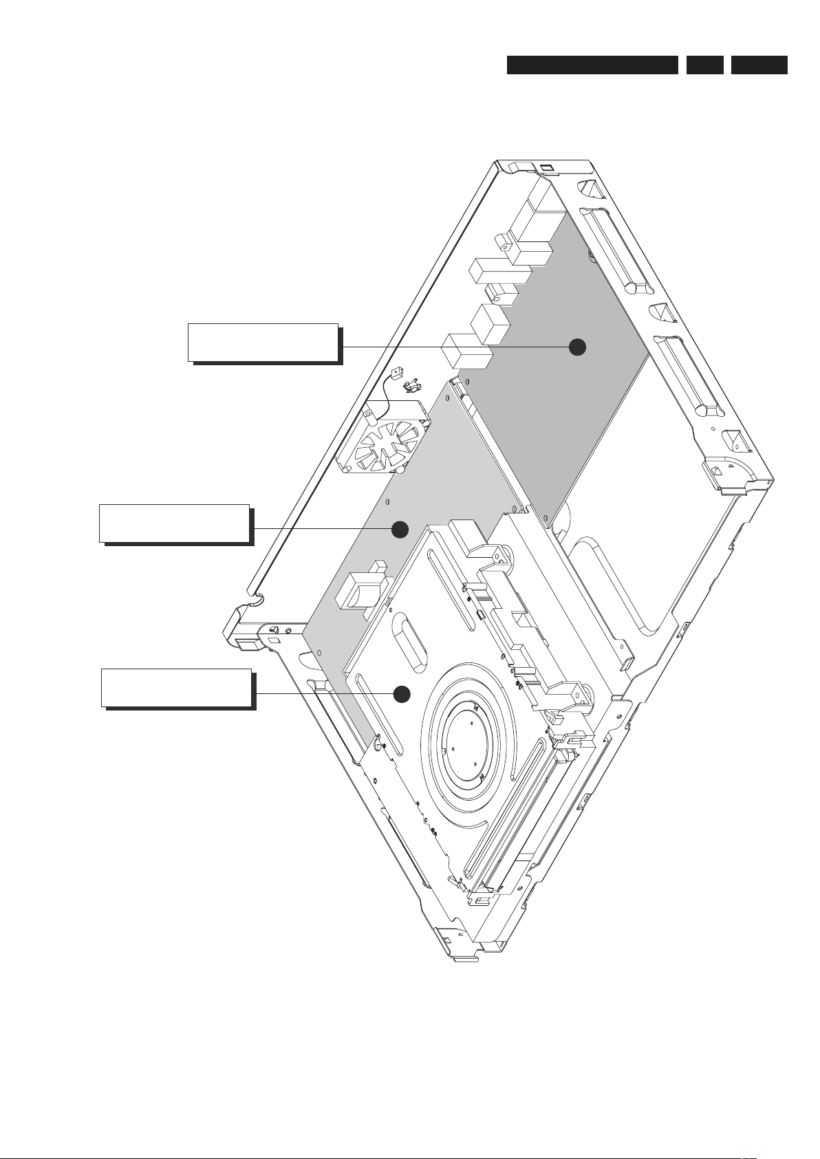
MAIN PCB
S.M.P.S PCB
BDP LOADER ASSY
1.11 PCB Location
Location PCB Drawing
3139 785 32970
1.
EN 3
EN 4
3139 785 32970
2.
Precautions
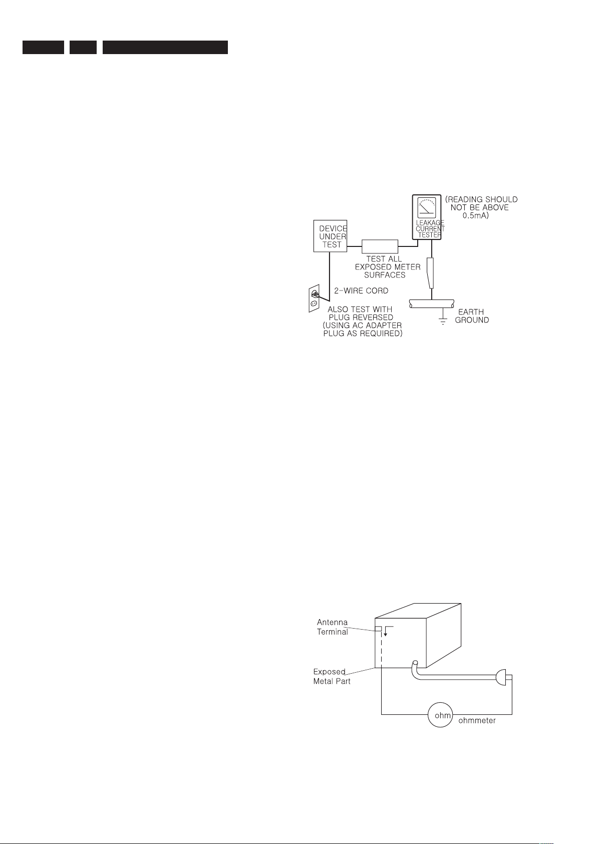
Fig. 1-1 AC Leakage Test
Fig. 1-2 Insulation Resistance Test
2. Precautions
2-1 Safety Precautions
1) Before returning an instrument to the customer,
always make a safety check of the entire
instrument, including, but not limited to, the
following items:
(1) Be sure that no built-in protective devices are
defective or have been defeated during servicing.
(1) Protective shields are provided to protect both
the technician and the customer. Correctly replace
all missing protective shields, including any
removed for servicing convenience.
(2) When reinstalling the chassis and/or other
assembly in the cabinet, be sure to put back in
place all protective devices, including, but not
limited to, nonmetallic control knobs, insulating
fish papers, adjustment and compartment covers/
shields, and isolation resistor/capacitor networks.
Do not operate this instrument or permit it to be
operated without all protective devices correctly
installed and functioning.
(2) Be sure that there are no cabinet openings
through which adults or children might be able
to insert their fingers and contact a hazardous
voltage. Such openings include, but are not limited
to, excessively wide cabinet ventilation slots, and
an improperly fitted and/or incorrectly secured
cabinet back cover.
(3) Leakage Current Hot Check-With the
instrument completely reassembled, plug the
AC line cord directly into a 230V(220V ~ 240V)
AC outlet. (Do not use an isolation transformer
during this test.) Use a leakage current tester
or a metering system that complies with
American National Standardsp institute (ANSI)
C101.1 Leakage Current for Appliances and
Underwriters Laboratories (UL) 1270 (40.7). With
the instrument’s AC switch first in the ON position
and then in the OFF position, measure from a
known earth ground (metal water pipe, conduit,
etc.) to all exposed metal parts of the instrument
(antennas, handle brackets, metal cabinets,
screwheads, metallic overlays, control shafts,
etc.), especially any exposed metal parts that offer
an electrical return path to the chassis. Any current
measured must not exceed 0.5mA. Reverse
the instrument power cord plug in the outlet and
repeat the test. See Fig. 1-1.
Any measurements not within the limits specified
herein indicate a potential shock hazard that must
be eliminated before returning the instrument to the
customer
(4) Insulation Resistance Test Cold Check-(1) Unplug
the power supply cord and connect a jumper wire
between the two prongs of the plug.
(2) Turn on the power switch of the instrument.
(3) Measure the resistance with an ohmmeter
between the jumpered AC plug and all exposed
metallic cabinet parts on the instrument, such as
screwheads, antenna, control shafts, handle brackets,
etc. When an exposed metallic part has a return path
to the chassis, the reading should be between 1 and
5.2 megohm. When there is no return path to the
chassis, the reading must be infinite. If the reading is
not within the limits specified, there is the possibility of
a shock hazard, and the instrument must be repaired
and rechecked before it is returned to the customer.
See Fig. 1-2.
.

Precautions
Precautions
3139 785 32970
2.
EN 5
2) Read and comply with all caution and safety
related notes on or inside the cabinet, or on the
chassis.
3) Design Alteration Warning-Do not alter or add
to the mechanical or electrical design of this
instrument.
Design alterations and additions, including but not
limited to, circuit modifications and the addition of
items such as auxiliary audio output connections,
might alter the safety characteristics of this
instrument and create a hazard to the user. Any
design alterations or additions will make you, the
servicer, responsible for personal injury or property
damage resulting therefrom.
4) Observe original lead dress. Take extra care to
assure correct lead dress in the following areas:
(1) near sharp edges, (2) near thermally hot parts
(be sure that leads and components do not touch
thermally hot parts), (3) the AC supply, (4) high
voltage, and (5) antenna wiring. Always inspect in
all areas for pinched, out-of-place, or frayed wiring,
Do not change spacing between a component and
the printed-circuit board. Check the AC power cord
for damage.
5) Components, parts, and/or wiring that appear to
have overheated or that are otherwise damaged
should be replaced with components, parts and/ or
wiring that meet original specifications.
Additionally, determine the cause of overheating
and/or damage and, if necessary, take corrective
action to remove any potential safety hazard.
6) Product Safety Notice-Some electrical and
mechanical parts have special safety-related
characteristics which are often not evident from
visual inspection, nor can the protection they give
necessarily be obtained by replacing them with
components rated for higher voltage, wattage, etc.
Parts that have special safety characteristics are
identified by shading, an ( )or a ( )on schematics
and parts lists. Use of a substitute replacement
that does not have the same safety characteristics
as the recommended replacement part might
create shock, fire and/or other hazards. Product
safety is under review continuously and new
instructions are issued whenever appropriate.

EN 6
3139 785 32970
2.
Precautions
2-2 Servicing Precautions
CAUTION : Before servicing units covered by this
service manual and its supplements, read and follow
the Safety Precautions section of this manual.Note : If
unforseen circumstances create conflict between the
following servicing precautions and any of the safety
precautions, always follow the safety precautions.
Remember: Safety First.
2-2-1 General Servicing Precautions
(1) a. Always unplug the instrument’s AC powercord
from the AC power source before (1) re-moving
or reinstalling any component, circuit board,
module or any other instrument assembly, (2)
disconnecting any instrument electrical plug or
other electrical connection, (3) connecting a test
substitute in parallel with an electrolytic ca pacitor
in the instrument.
b. Do not defeat any plug/socket B+ voltage
interlocks with which instruments covered by this
service manual might be equipped.
c. Do not apply AC power to this instrument and/or
any of its electrical assemblies unless all solidstate device heat sinks are correctly installed.
d. Always connect a test instrument’s ground lead
to the instrument chassis ground before connecting
the test instrument positive lead. Alwaysremove
the test instrument ground lead last.
(4) An insulation tube or tape is sometimes used
and some components are raised above the
printed wiring board for safety. The internal wiring
is sometimes clamped to prevent contact with
heating components. Install such elements as they
were.
(5) After servicing, always check that the removed
screws, components, and wiring have been
installed correctly and that the portion around the
serviced part has not been damaged and so on.
Further, check the insulation between the blades
of the attachment plug and accessible conductive
parts.
2-2-2 Insulation Checking Procedure
Disconnect the attachment plug from the AC outlet
and turn the power ON. Connect the insulation resistance meter (500V) to the blades of the attachment
plug. The insulation resistance between each blade of
the attachment plug and accessible conductive parts
(see note) should be more than 1 Megohm.
Note : Accessible conductive parts include metal
panels,input terminals, earphone jacks, etc.
Note : Refer to the Safety Precautions section ground
lead last.
(2) The service precautions are indicated or printed
on the cabinet, chassis or components. When
servicing, follow the printed or indicated service
precautions and service materials.
(3) The components used in the unit have a specified
flame resistance and dielectric strength. When
replacing components, use components which
have the same ratings. Components identified
by shading, by ( ) or by ( ) in the circuit diagram
are important for safety or for the characteristics
of the unit. Always replace them with the exact
replacement components.

2-3 ESD Precautions
Electrostatically Sensitive Devices (ESD)
Precautions
3139 785 32970
2.
EN 7
Some semiconductor (solid state) devices can be
dam-agedeasily by static electricity.Such components
commonly are called Electrostatically Sensitive
Devices(ESD). Examples of typical ESD devices are
integrated circuits and some field-effect transistors
and semiconductor chip components. Thefollowing
techniques should be used to help reducethe
incidence of component damage caused by static
electricity.
(1) Immediately before handling any semiconductor
component or semiconductor-equipped assembly,
drain off any electrostatic charge on your body
by touching a known earth ground. Alternatively,
obtain and wear a commercially available
discharging wrist strap device, which should be
removed for potential shock reasons prior to
applying power to the unit under test.
(2) After removing an electrical assembly equipped
with ESD devices, place the assembly on a
conductive surface such as aluminum foil, to
prevent electrostatic charge buildup or exposure
of the assembly.
CAUTION : Be sure no power is applied to the chassis
or circuit, and observe all other safety precautions.
(8) Minimize bodily motions when handling
unpackaged replacement ESD devices.
(Otherwise harmless motion such as the brushing
together of your clothes fabric or the lifting of your
foot from a carpeted floor can generate static
electricity sufficient to damage an ESD device).
(3) Use only a grounded-tip soldering iron to solder or
unsolder ESD devices.
(4) Use only an anti-static solder removal devices.
Some solder removal devices not classified as
“anti-static” can generate electrical charges
sufficient to damage ESD devices.
(5) Do not use freon-propelled chemicals. These can
generate electrical charges sufficient to damage
ESD devices.
(6) Do not remove a replacement ESD device from
its protective package until immediately before
your are ready to install it.(Most replacement
ESD devices are packaged with leads electrically
shorted together by conductive foam, aluminum foil
or comparable conductive materials).
(7) Immediately before removing the protective
materials from the leads of a replacement ESD
device, touch the protective material to the chassis
or circuit assembly into which the device will be
installed.
EN 8
3139 785 32970
2.
Precautions
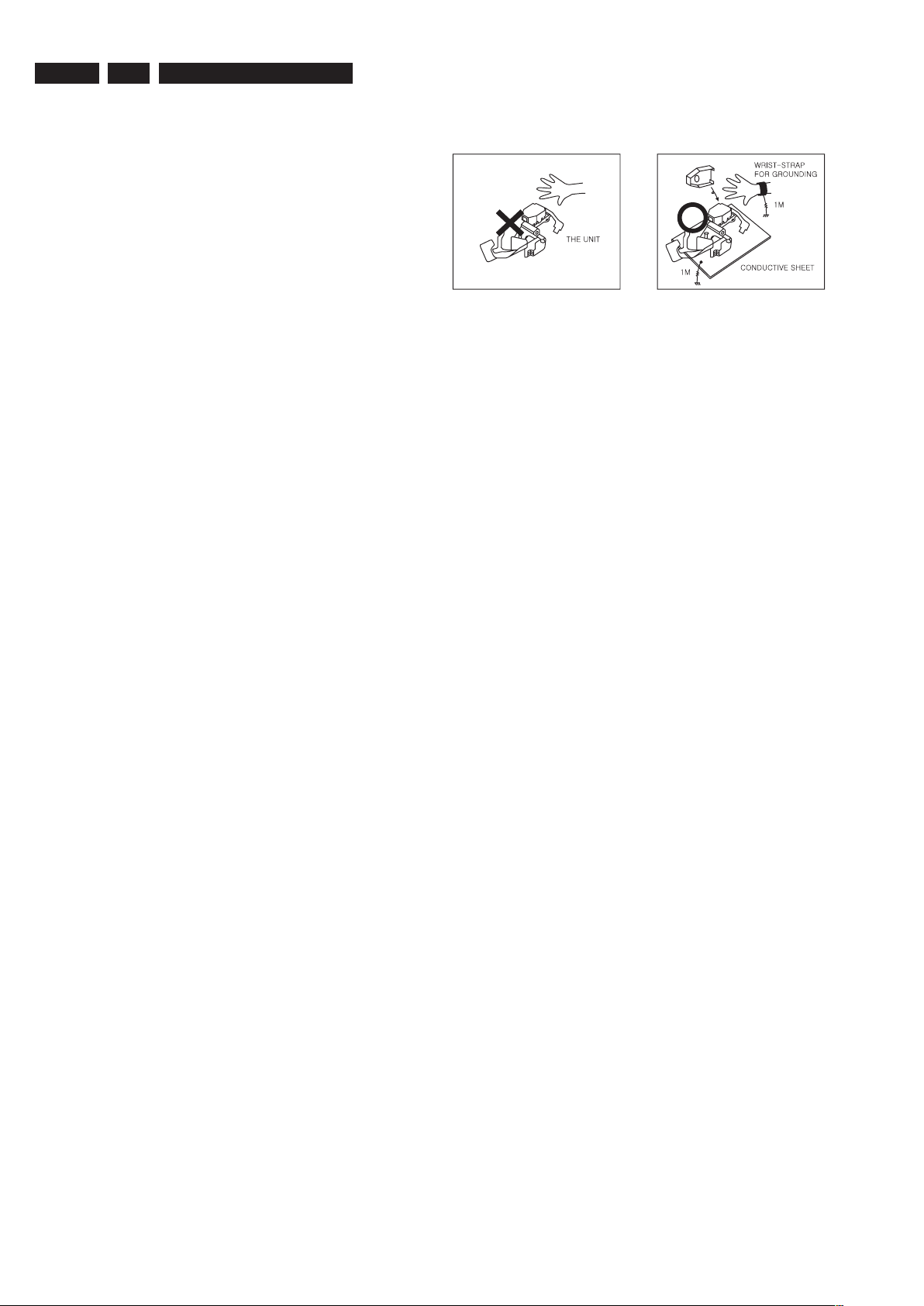
Fig.1-3
2-4 Handling the optical pick-up
The laser diode in the optical pick up may suffer
electrostatic breakdown because of potential static
electricity from clothing and your body.
The following method is recommended.
(1) Place a conductive sheet on the work bench (The
black sheet used for wrapping repair parts.)
(2) Place the set on the conductive sheet so that the
chassis is grounded to the sheet.
(3) Place your hands on the conductive sheet (This
gives them the same ground as the sheet.)
(4) Remove the optical pick up block
(5) Perform work on top of the conductive sheet. Be
careful not to let your clothes or any other static
sources to touch the unit.
Be sure to put on a wrist strap grounded to the
sheet.
Be sure to lay a conductive sheet made of copper
etc. Which is grounded to the table.
(6) Short the short terminal on the PCB, which is
inside the Pick-Up ASS’Y, before replacing the
Pick- Up. (The short terminal is shorted when the
Pick- Up Ass’y is being lifted or moved.)
(7) After replacing the Pick-up, open the short terminal
on the PCB.

Precautions
3139 785 32970
2.
EN 9
2.5 Lead Free Requirement
Information about Lead-free produced sets
Philips CE is starting production of lead-free sets from
1.1.2005 onwards.
INDENTIFICATION:
Regardless of special logo (not always indicated)
One must treat all sets from 1 Jan 2005 onwards,
according next rules.
Example S/N:
Bottom line of typeplate gives a 14-digit S/N. Digit 5&6 is the year, digit 7&8 is
the week number, so in this case 1991 wk 18
So from 0501 onwards = from 1 Jan 2005 onwards
• Special information for BGA-ICs:
Do not re-use BGAs at all.
• For sets produced before 1.1.2005 (except products of
• On our website www.atyourservice.ce.Philips.com you
BGA-de-/soldering (+ baking instructions)
Heating-profiles of BGAs and other ICs used in Philips-
You will find this and more technical information within
For additional questions please contact your local repair-helpdesk.
- always use the 12nc-recognizable soldering
temperature profile of the specific BGA (for de-soldering
always use the lead-free temperature profile, in case of
doubt)
- lead free BGA-ICs will be delivered in so-called ‘drypackaging’ (sealed pack including a silica gel pack) to
protect the IC against moisture. After opening, dependent
of MSL-level seen on indicator-label in the bag, the
BGA-IC possibly still has to be baked dry. (MSL=Moisture
Sensitivity Level). This will be communicated via AYSwebsite.
2004), containing leaded solder-alloy and components,
all needed spare-parts will be available till the end of the
service-period. For repair of such sets nothing changes.
find more information to:
sets
the “magazine”, chapter “workshop news”.
Important note: In fact also products of year 2004 must be treated in this way as long as
you avoid mixing solder-alloys (leaded/ lead-free). So best to always use SAC305 and the
higher temperatures belong to this.
Due to lead-free technology some rules have to be respected by the
workshop during a repair:
• Use only lead-free solder alloy Philips SAC305 with
• Use only adequate solder tools applicable for lead-free
o To reach at least a solder-temperature of 400°C,
o To stabilize the adjusted temperature at the solder-tip
o To exchange solder-tips for different applications.
• Adjust your solder tool so that a temperature around
• Mix of lead-free solder alloy / parts with leaded solder
• Use only original spare-parts listed in the Service-
order code 0622 149 00106. If lead-free solder-pate
is required, please contact the manufacturer of your
solder-equipment. In general use of solder-paste within
workshops should be avoided because paste is not easy
to store and to handle.
solder alloy. The solder tool must be able
360°C – 380°C is reached and stabilized at the solder
joint. Heating-time of the solder-joint should not exceed
~ 4 sec. Avoid temperatures above 400°C otherwise
wear-out of tips will rise drastically and flux-fluid will be
destroyed. To avoid wear-out of tips switch off un-used
equipment, or reduce heat.
alloy / parts is poss ble but PHILIPS recommends
strongly to avoid mixed solder alloy types (leaded and
lead-free).
If one cannot avoid or does not know whether product is
lead-free, clean carefully the solder-joint from old solder
alloy and re-solder with new solder alloy (SAC305).
Manuals. Not listed standard-material (commodities) has
to be purchased at external companies.
EN 10
3139 785 32970
3.
Disassembly Instructions
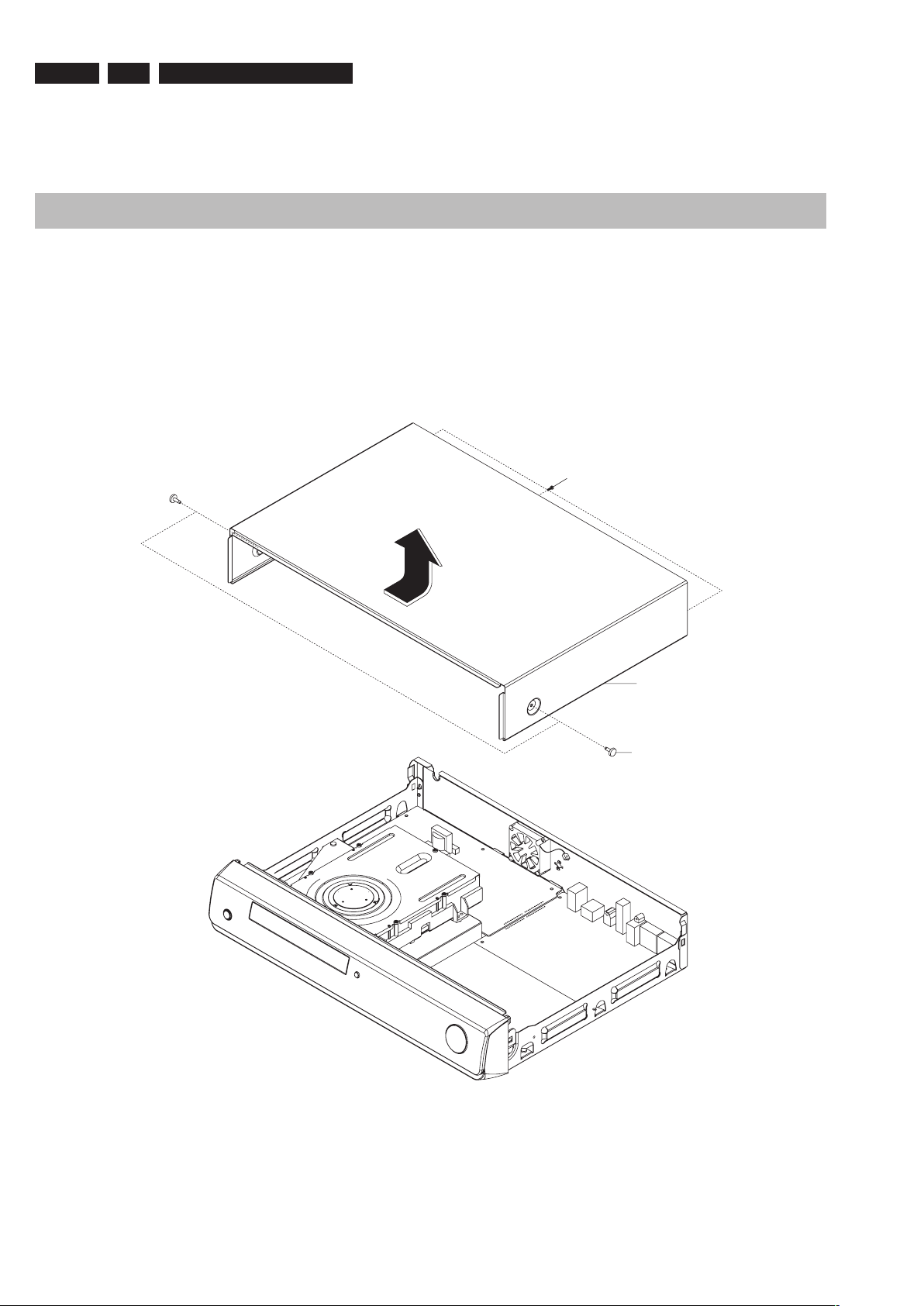
Fig. 3-1 Top Cabinet Removal
3 SCREWS
(3X10 B)
TOP CABINET
2 SCREWS
(3X8 B)
2
3
1
3. Disassembly and Reassembly
Cabinet and PCB
CAUTION : Connector Must be removed with care
3-1 Top Cabinet Removal
1) Remove 5 Screws 1 2.
2) Lift up the Top Cabinet 3 in direction of arrow.
Disassembly Instructions
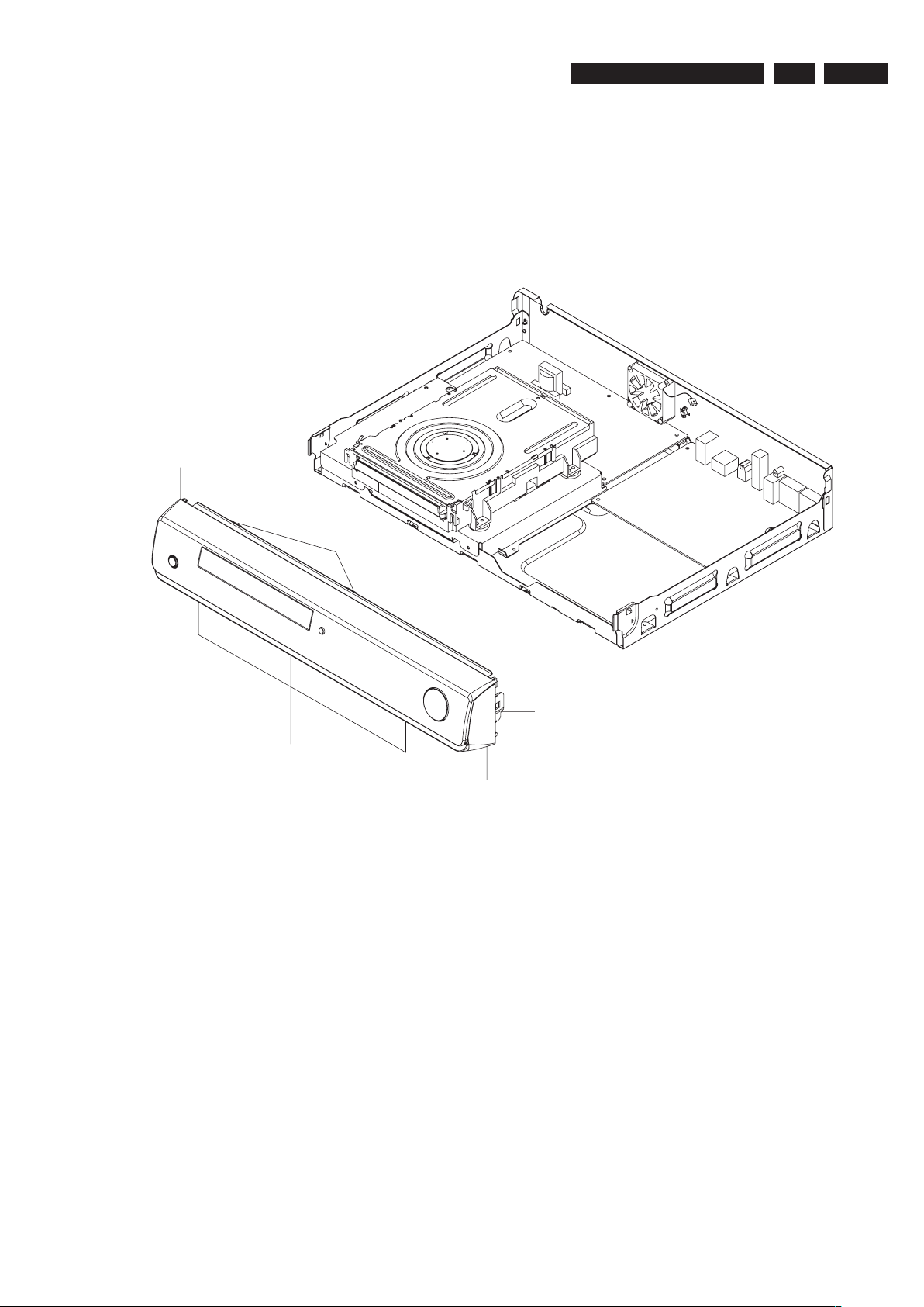
Fig. 3-2 Ass’y Front-Cabinet Removal
1 HOOK
ASS’Y FRONT-CABINET
2 HOOKS
3 HOOKS
1 HOOK
1
4
3
2
5
3-2 Ass’y Front-Cabinet Removal
1) Release 7 Hooks 1, 2, 3, 4 and Ass’y Front-Cabinet 5.
3139 785 32970
3.
EN 11
EN 12
3139 785 32970
3.
Disassembly Instructions
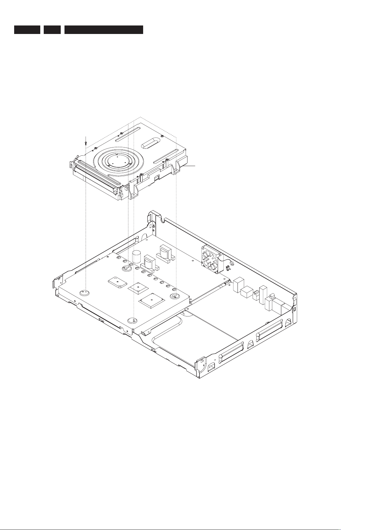
Fig. 3-3 Ass’y Deck Removal
4 SCREWS
(3X10 W)
ASS’Y DECK
1
2
3-3 Ass’y Deck Removal
1) Remove 4 Screws 1 from the Ass’y Deck 2 and lift it up.
Disassembly Instructions
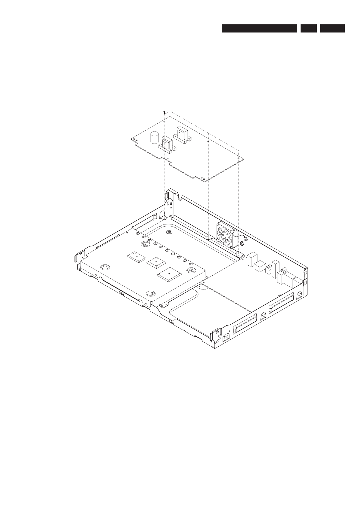
Fig. 3-4 S.M.P.S PCB Removal
6 SCREWS
(3X8 W)
S.M.P.S PCB
1
2
3-4 S.M.P.S PCB Removal
1) Remove 3 Screws 1, from the S.M.P.S PCB 2 and lift it up.
3139 785 32970
3.
EN 13
EN 14
3139 785 32970
3.
Disassembly Instructions
Fig. 3-5 Main PCB Removal
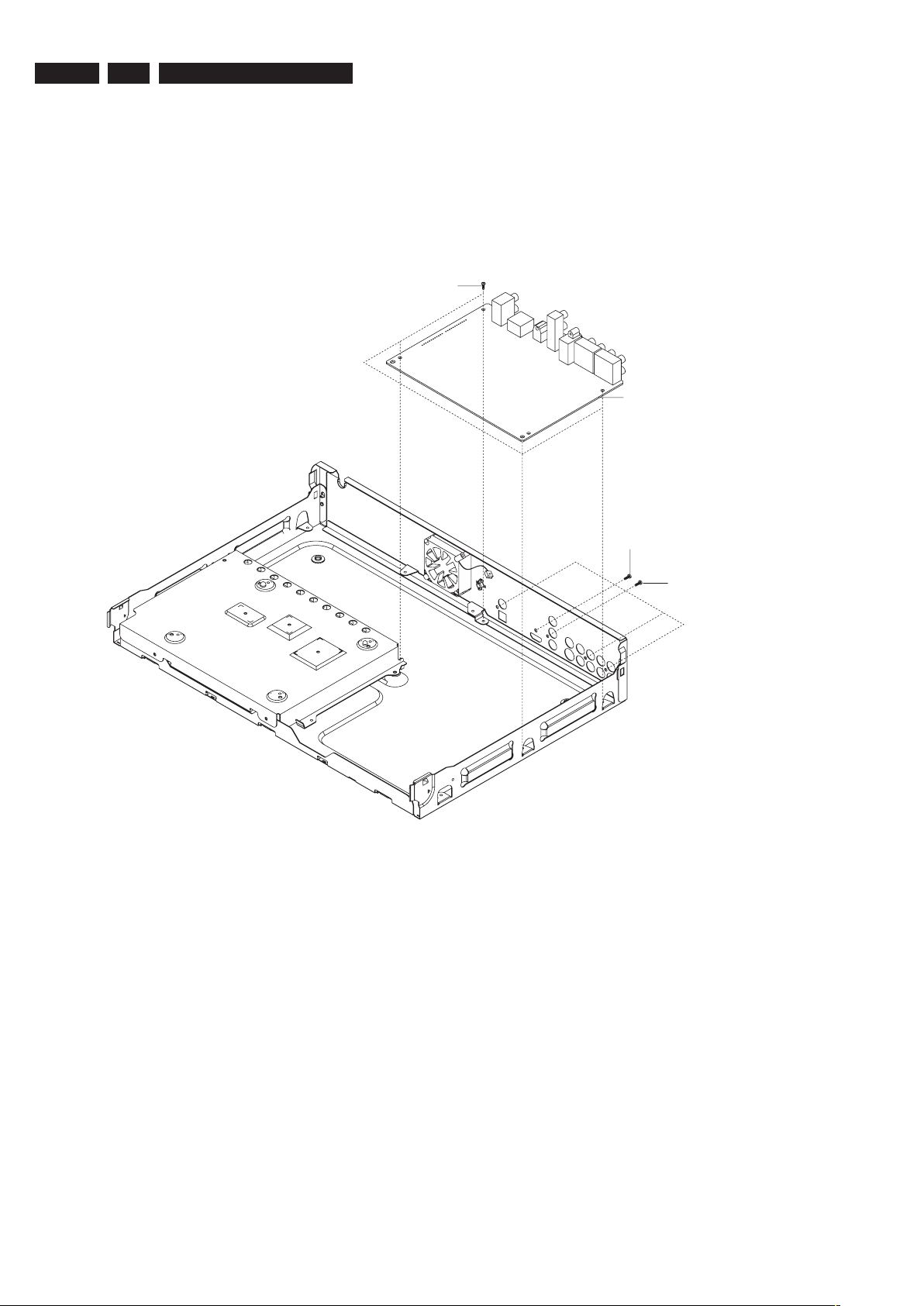
MAIN PCB
1 SCREW
(3X6 B)
4 SCREWS
(3X6 W)
5 SCREWS
(3X10 B)
1
4
2
3
3-5 Main PCB Removal
1) Remove 10 Screws 1, 2, 3 from the Main PCB 4 and lift it up.
Disassembly Instructions
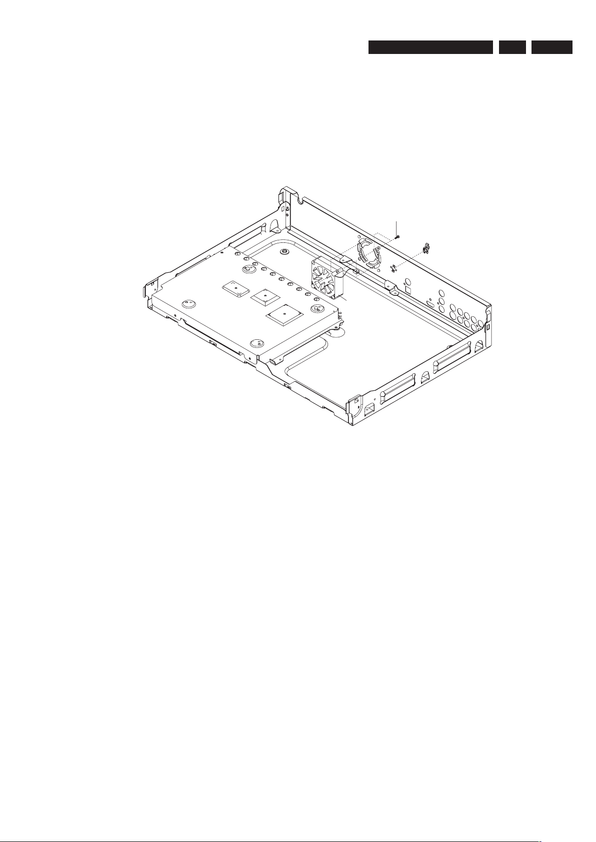
Fig. 3-6 FAN Removal
2 SCREWS
(5X14 S)
FAN
1
2
3-6 FAN Removal
1) Remove 2 Screws 1 from the Fan 2 and lift it up.
3139 785 32970
3.
EN 15
EN 16
3139 785 32970
4.
Trouble Shooting
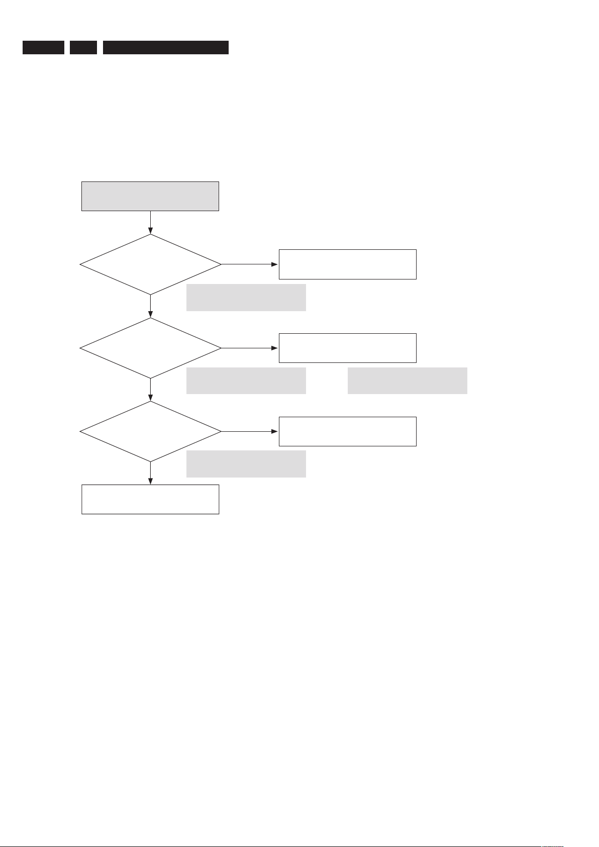
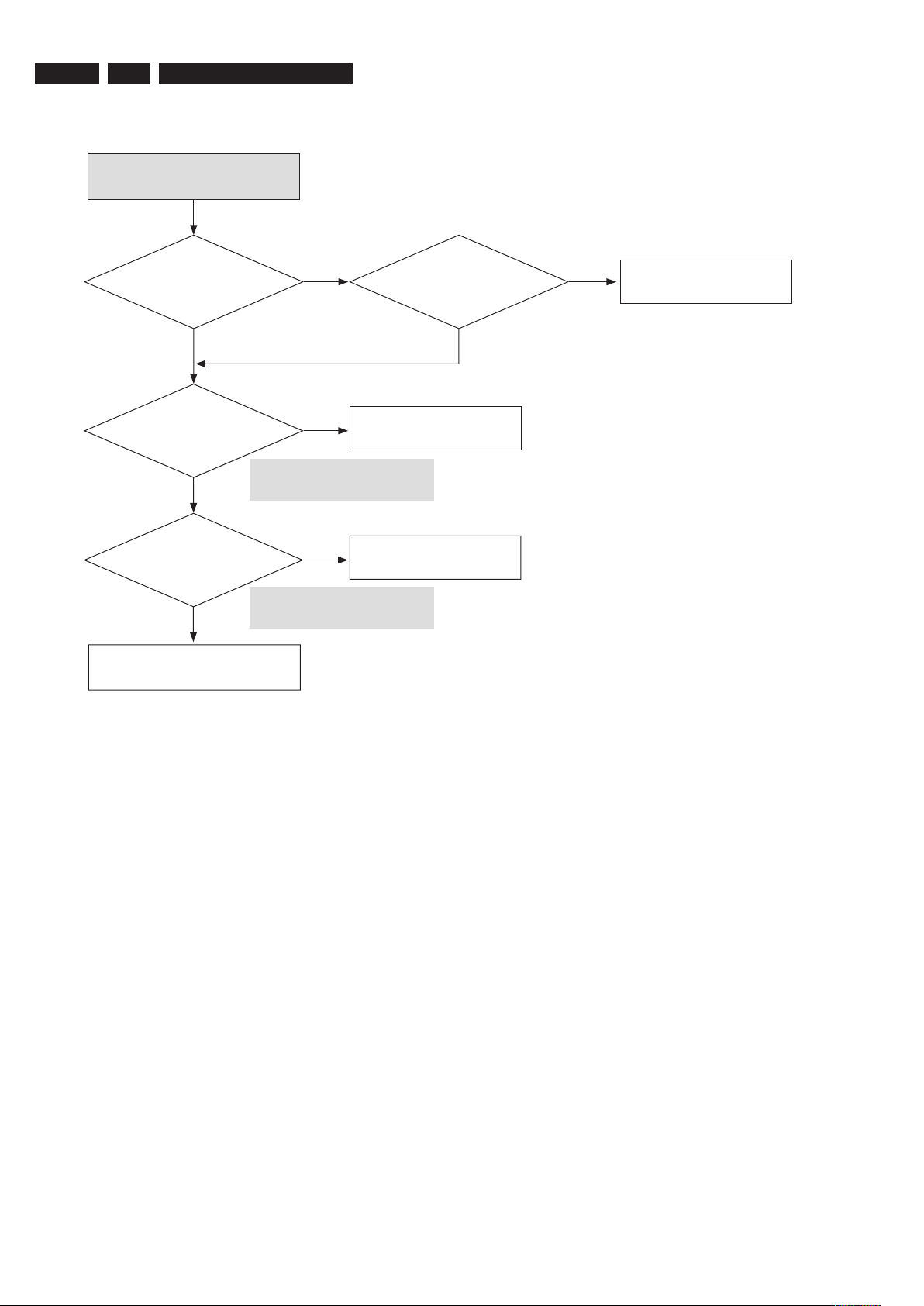
NO Power Detected
(Stand by LED OFF)
F1S01 is normal?
C1S01
voltage
is normal voltage?
Switching
operation
of IC1S11 is normal?
Change the SMPS PCB
Change fuse
Change BD1
Change IC1S11
No
Yes
No
No
Yes
Yes
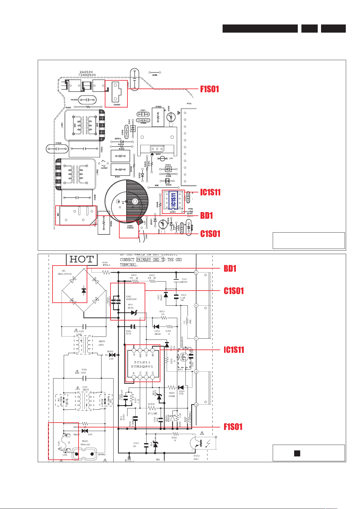
Refer to Fig. 4-1
Refer to Fig. 4-1 Refer to Fig. 4-1
Refer to Fig. 4-1
4 Trouble Shooting
Trouble Shooting
Fig. 4-1
Refer to S.M.P.S. PCB
COMPONENT SIDE
Refer to 1 (Circuit Diagrams)
3139 785 32970
4.
EN 17
EN 18
3139 785 32970
4.
Trouble Shooting
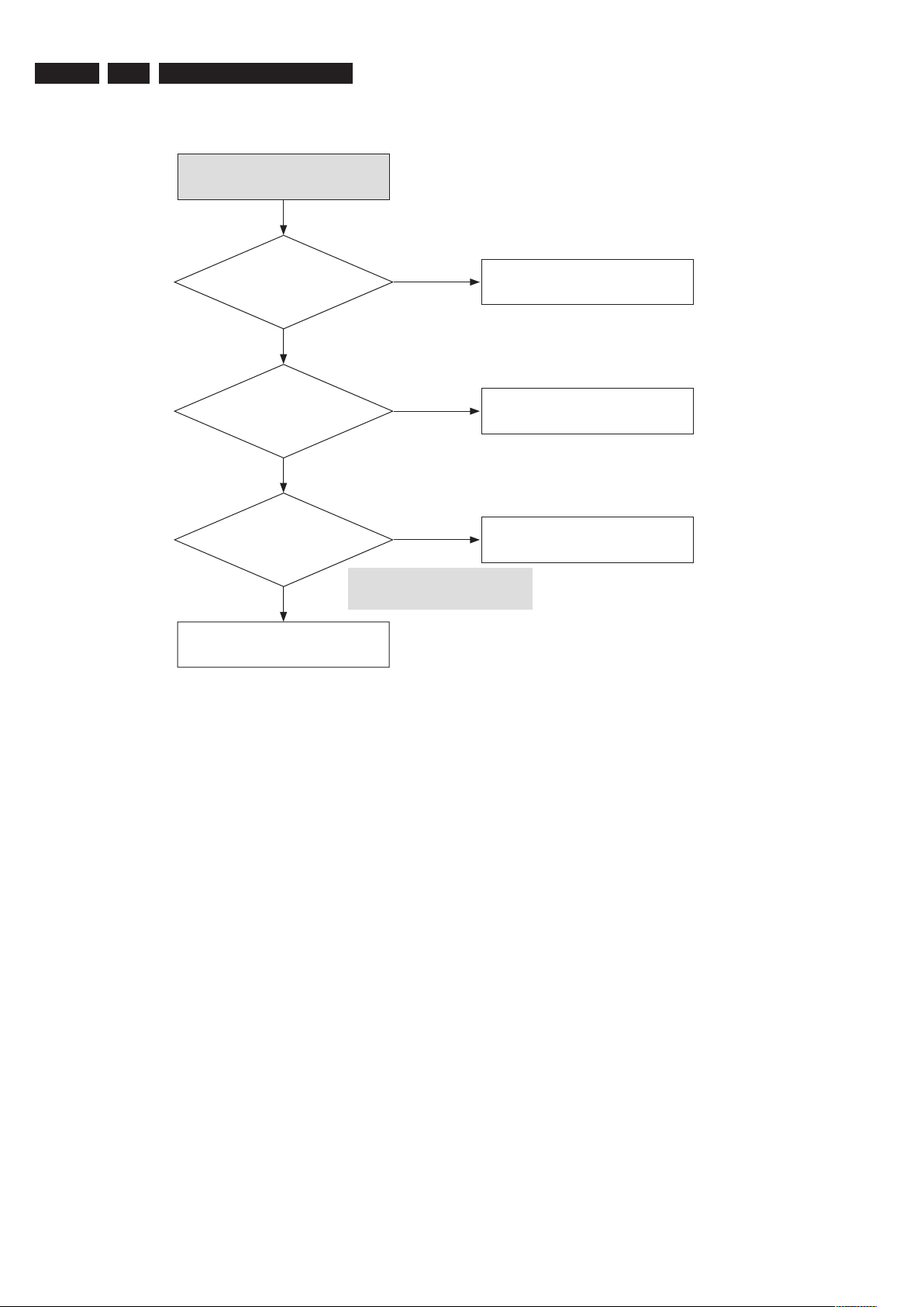
There’s no Digital Audio Out
Check
Current Digital Audio
Setting is PCM.
Set to Bitstream
No
Yes
Check
the A/V Receiver can
Decode Current
Bit-Steam
No
Yes
Check
Digital Audio Data
at AIC 1 (Pin 2,4,6)
No
Yes
Check AIC1 soldering or
replace AIC1
Digital Audio cable error
Check the
Audio Data at AIC1
(Pin 13)
No
Yes
Replace the Main PCB
Refer to Fig. 4-2
Refer to Fig. 4-2
Trouble Shooting
Fig. 4-2
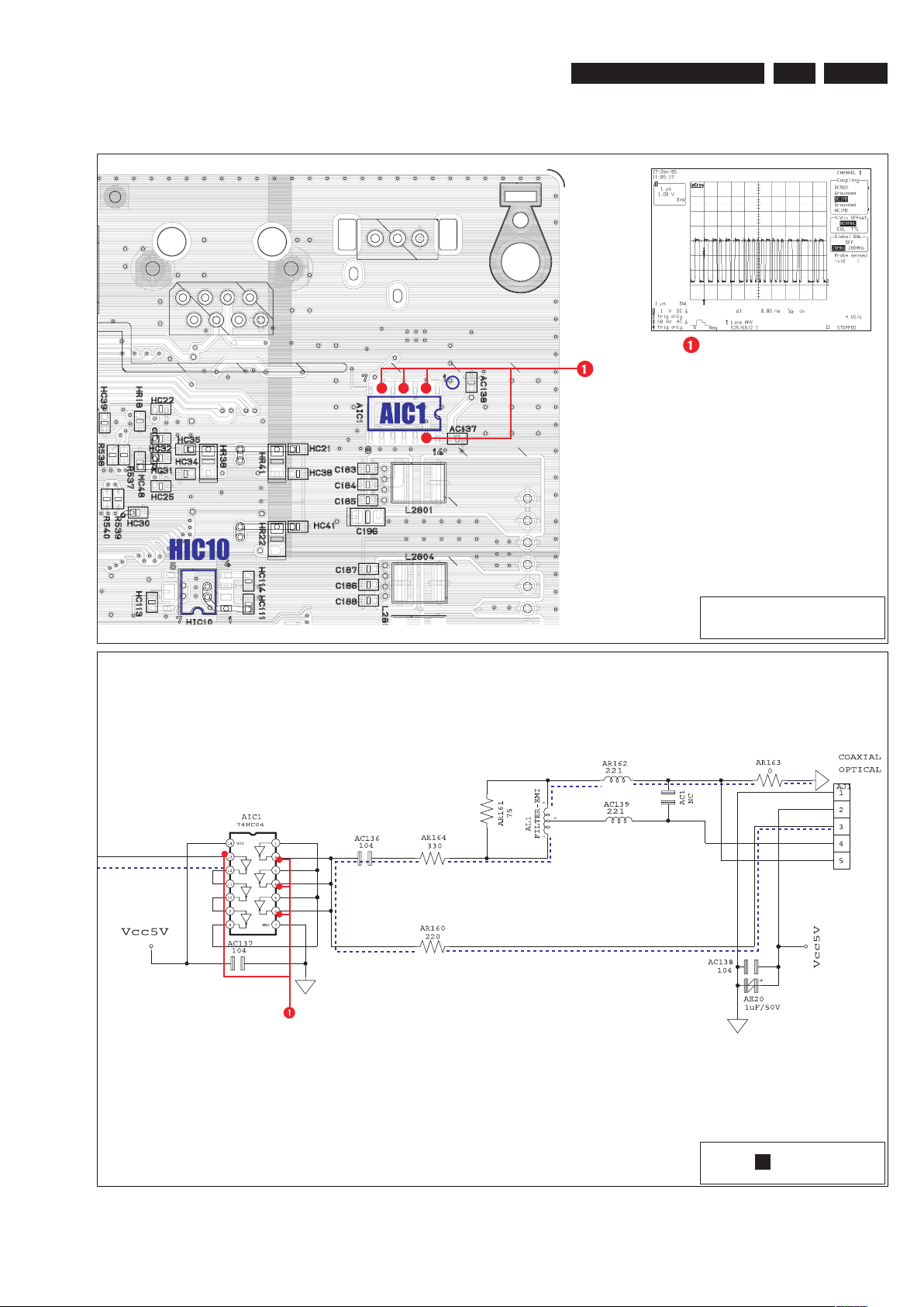
DIGITAL AUDIO DATA
AIC1 (Pin2,4,6,13)
Refer to Main PCB
CONDUCTOR SIDE
Refer to 9 (Circuit Diagrams)
3139 785 32970
4.
EN 19
EN 20
3139 785 32970
4.
Trouble Shooting
There is no Audio Output
Check
the Audio
signal at PIN 13,14,15,16
of AIC2
Check
the Audio
signal at pin1,2,37~48 of
AIC2
Check
the Audio
signal at AIC4,5,6,7
Audio cable error
Replace the main PCB
Check AIC2 soldering or replace
AIC2
Check AIC4~7 soldering of
peripheral devices
No
Yes
No
No
Yes
Yes
Refer to Fig. 4-3
Trouble Shooting
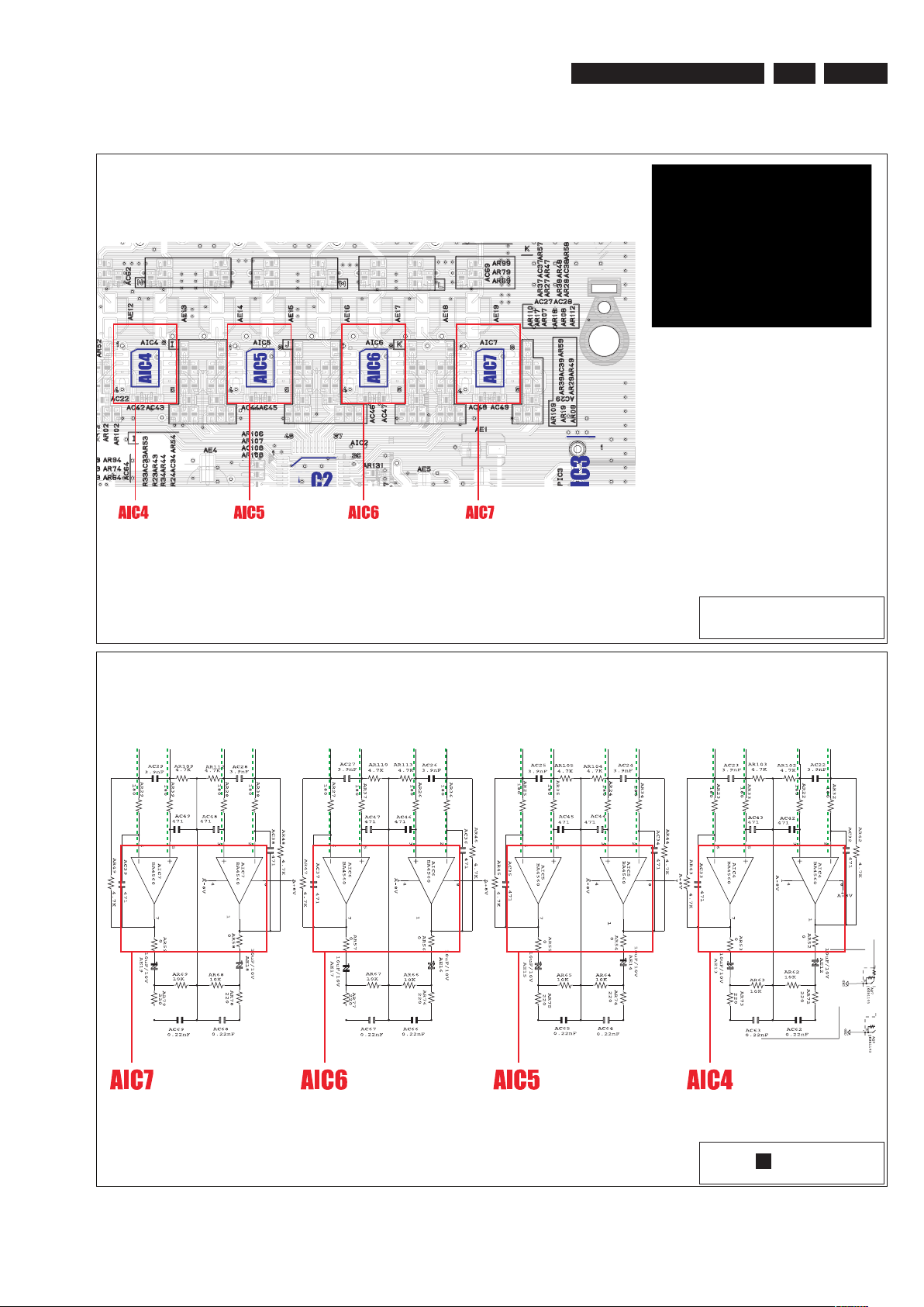
Fig. 4-3
ANALOG AUDIO DATA(AIC4,5,6,7)
Refer to Main PCB
COMPONENT SIDE-2
Refer to 9 (Circuit Diagrams)
3139 785 32970
4.
EN 21
 Loading...