

Page 1
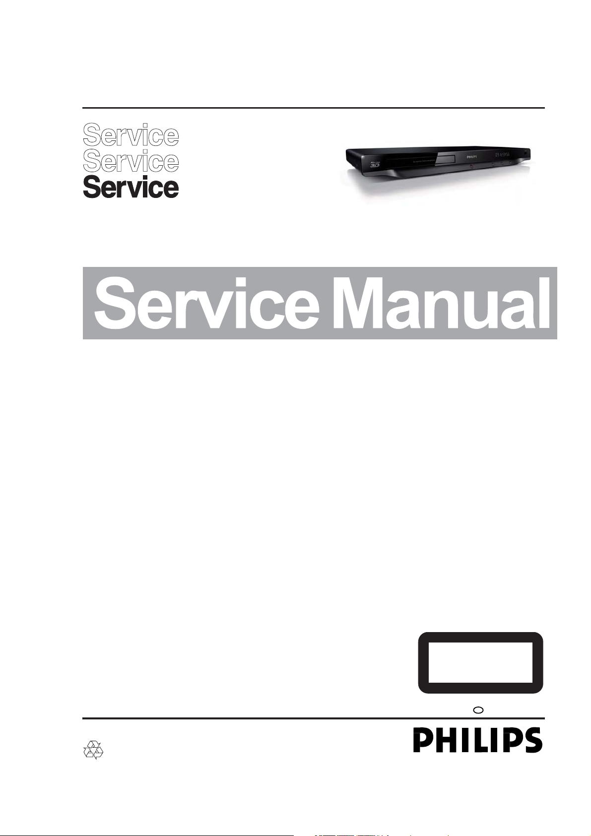
Blu-ray Disc Player
BDP5200/12/05/51/98/55/K93/X78
TABLE OF CONTENTS
Page
Location of PCB Boards & version variation & repair scenario matrix.....................
Production Specifications ...............................................................................................1-2
Remote control ...............................................................................................................1-3
Brife guide ......................................................................................................................1-
Safety Instruction, Warning & Notes...............................................................................1-
Mechanical and Dismantling Instructions .......................................................................2-1
Software Version & Upgrades.........................................................................................3-1
Trouble Shooting Chart .....................................................................................................-1
Set Block & Wiring Diagrams ............................................................................5-1
Electrical Diagrams and PCB layouts ................................................................6-1
Set Mechanical Exploded view ....................................................................................... -1
Revision List ...................................................................................................................
©
Copyright 2010 Philips Consumer Electronics B.V. Eindhoven, The Netherlands
All rights reserved. No part of this publication may be reproduced, stored in a retrieval system or
transmitted, in any form or by any means, electronic, mechanical, photocopying, or otherwise without
the prior permission of Philips.
Published by Helen-RY 1116 Service Audio Printed in The Netherlands Subject to modification
1-1
4
9
4
7
8
-1
CLASS 1
LASER PRODUCT
GB
GB
313978535553
©
Version 1.3
Version 0.0
Page 2
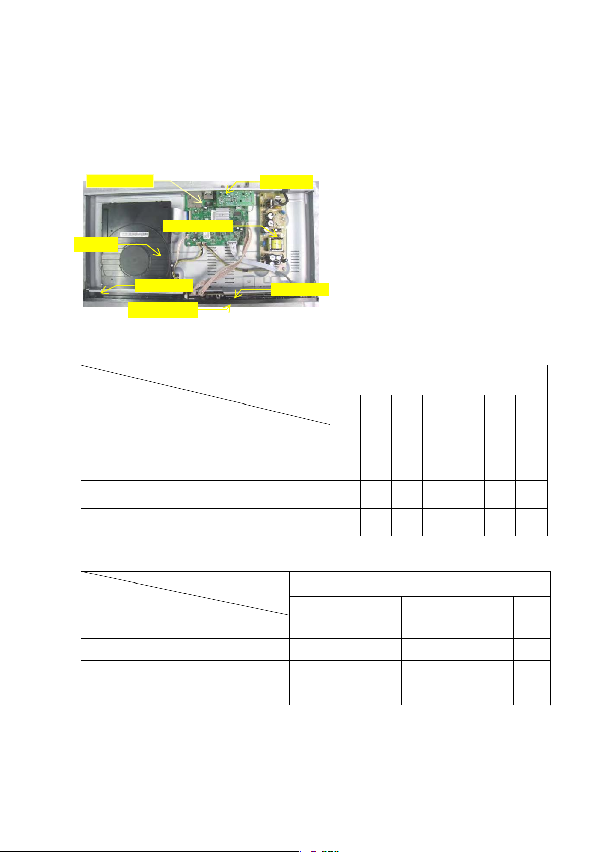
LOCATION OF PCB BOARDS˖
1-1
MAIN BOARD
AV BOARD
POWER BOARD
LOADER
FE BOARD
FRONT CABINET
KE BOARD
Version Variation
Type/Versions
Features
Power supply rating:220-240V ,60Hz X
Power supply rating:230-240V ,60Hz
Power supply rating:110-240V ,50Hz,60Hz
Power consumption:18W X X X X X X X
BDP5200
/12 /05 /51 /98 /55 K93 X/78
X
X
X X X X
Repair Scenario Matrix
Type/Versions
Board in used
Main Board Bd Bd Bd Bd Bd Bd Bd
Power Board Bd Bd Bd Bd Bd Bd Bd
AV Board Bd Bd Bd Bd Bd Bd Bd
Loader Bd Bd Bd Bd Bd Bd Bd
*Bd:Board Level Replacement
*C:Component Level Repair
/12 /05 /51 /98 /55 K93 X/78
BDP5200
Page 3
1-2
BDP5200/12/05/51/98/55/K93/X78
Product Specifications
Note
6SHFLÀFDWLRQVDUHVXEMHFWWRFKDQJHZLWKRXWQRWLFH
Region code
This player can play discs with the following region codes.
DVD Blu-ray Countries
Europe, United Kingdom
B
Playable media
BD-Video, BD 3D
DVD-Video, DVD+R/+RW, DVD-R/-RW,
DVD+R/-R DL (Dual Layer)
VCD/SVCD
$XGLR&'&'5&'5:03PHGLD
WMA media,
DivX (Ultra)/DivX Plus HD media, MKV media
USB storage device
File format
Video: .avi, .divx, .mp4, .mkv, .wmv
Audio: .mp3, .wma, .wav
Picture: .jpg, .gif, .png
Video
Signal system: PAL / NTSC
Composite video output: 1 Vp-p (75 ohm)
HDMI output 480p, 576p, 720p, 1080i, 1080p,
1080p24
Audio
2 Channel analog output
Audio Front L&R : 2 Vrms (> 1 kohm)
Digital output: 0.5 Vp-p (75 ohm)
Coaxial
HDMI output
Sampling frequency:
MP3: 32 kHz, 44.1 kHz, 48 kHz
WMA: 44.1 kHz, 48 kHz
Constant bit rate:
MP3: 112 kbps - 320 kpbs
WMA: 48 kpbs - 192 kpbs
JPEG files,
USB
Compatibility: Hi-Speed USB (2.0)
Class support: USB Mass Storage Class
File system: FAT16, FAT32
Support HDD (a portable hard drive disc):
an external power s
Main unit
BDP5200/12/51:
Power supply rating: AC 220-240V~, 50 Hz
BDP5200/05:
Power supply rating: AC 230-240V~, 50 Hz
BDP5200/98/55/K93/X78:
Power supply rating: AC 110-240V~, 50 Hz , 60Hz
Power consumption: 18 W
Power consumption in standby mode: < 0.18 W
Dimensions (w x h x d): 435 x 42 x 208.5 (mm)
Net Weight: 1.65 kg
Accessories supplied
Remote control and batteries
User manual
CD-ROM built in multi-lingual user manua
(Continental Europe o
/DVHU6SHFLÀFDWLRQ
Laser Type (Diode): AlGaInN (BD), AlGaInP
(DVD/CD)
Wave length: 400 ~ 410nm (BD), 650 ~ 663nm
(DVD), 770 ~80 0nm (CD)
Output power (Max ratings): 20mW (BD), 7mW
(DVD), 7mW (CD)
ource may be needed.
nly)
Page 4
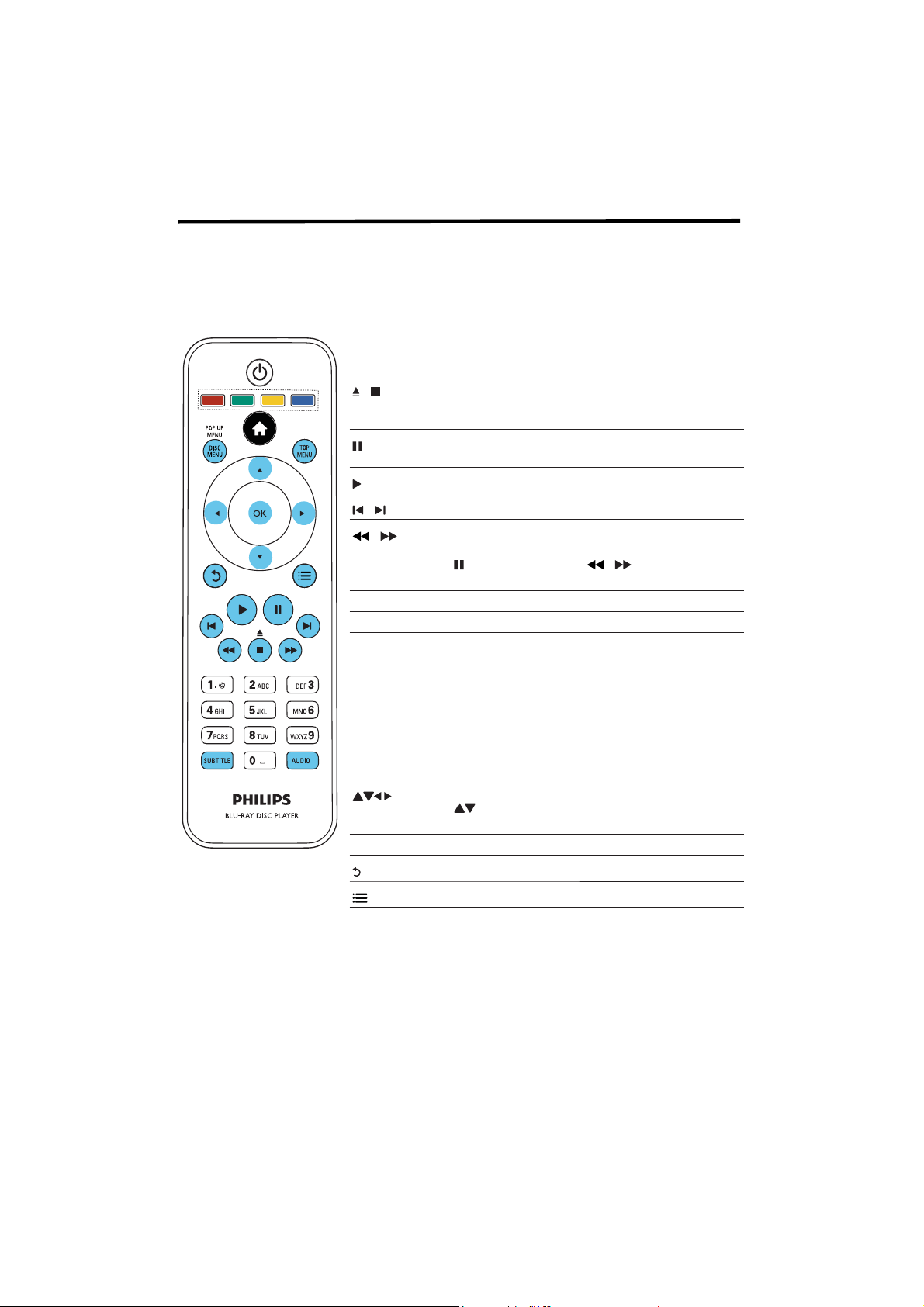
Remote Control
During play, press the following buttons to control.
Button Action
/
/
/
AUDIO Select an audio language or channel.
SUBTITLE Select a subtitle language.
DISC
MENU /
POP-UP
MENU
TOP
MENU
Color
buttons
OK &RQÀUPDVHOHFWLRQRUHQWU\
1-3
Stop play.
Press and hold (more than 4 seconds) to open or close
the disc compartment.
Pause play.
Press repeatedly to slow forward frame by frame.
Star t or resume play.
6NLSWRWKHSUHYLRXVRUQH[WWUDFNFKDSWHURUÀOH
Fast backward or forward.
Press repeatedly to change the search speed.
Press
once, and then press / to slow backward
or forward.
Access or exit the disc menu.
Access the main menu of a video disc.
Select tasks or options for Blu-ray discs.
Navigate the menus.
Press
clockwise during slideshow.
Return to a previous display menu.
Access more options during play.
to rotate a picture clockwise or counter-
Page 5

O
A
U
1
Brife Guide
Register your product and get support at
www.philips.com/welcome
EN User manual
1-4
BDP5200
BDP5200
PC & Mac
VIDE
COAIAL
COAXIAL AUDIO LINE OUT
DIO LINE O
HDMIVIDEO
T
( )
Page 6
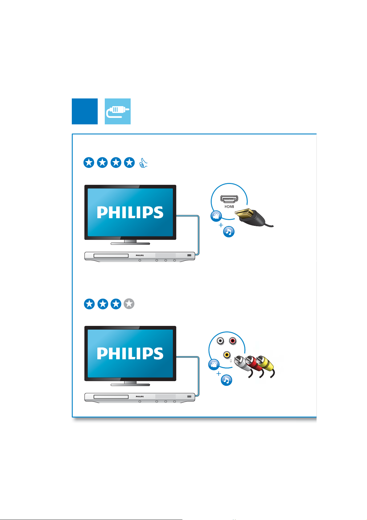
2
O
T
1-5
1 HDMI
HDMI { VIDEO { COAXIAL { AUDIO LINE OUT
2 VIDEO+AUDIO LINE OUT
{HDMI VIDEO { COAXIAL AUDIO LINE OUT
AUDIO LINE OUT
LINE
OU
VIDEO
VIDE
Page 7
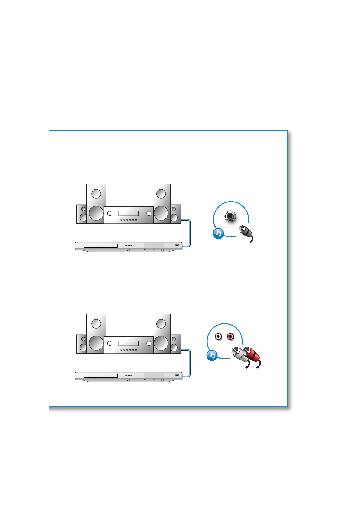
1-6
3 COAXIAL
4 AUDIO LINE OUT
{HDMI { VIDEO COAXIAL { AUDIO LINE OUT
COAXIAL
{HDMI { VIDEO { COAXIAL AUDIO LINE OUT
AUDIO LINE OUT
Page 8
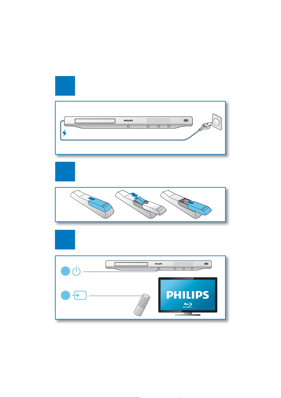
3
4
1-7
5
1
2
SOURCE
TV
Page 9
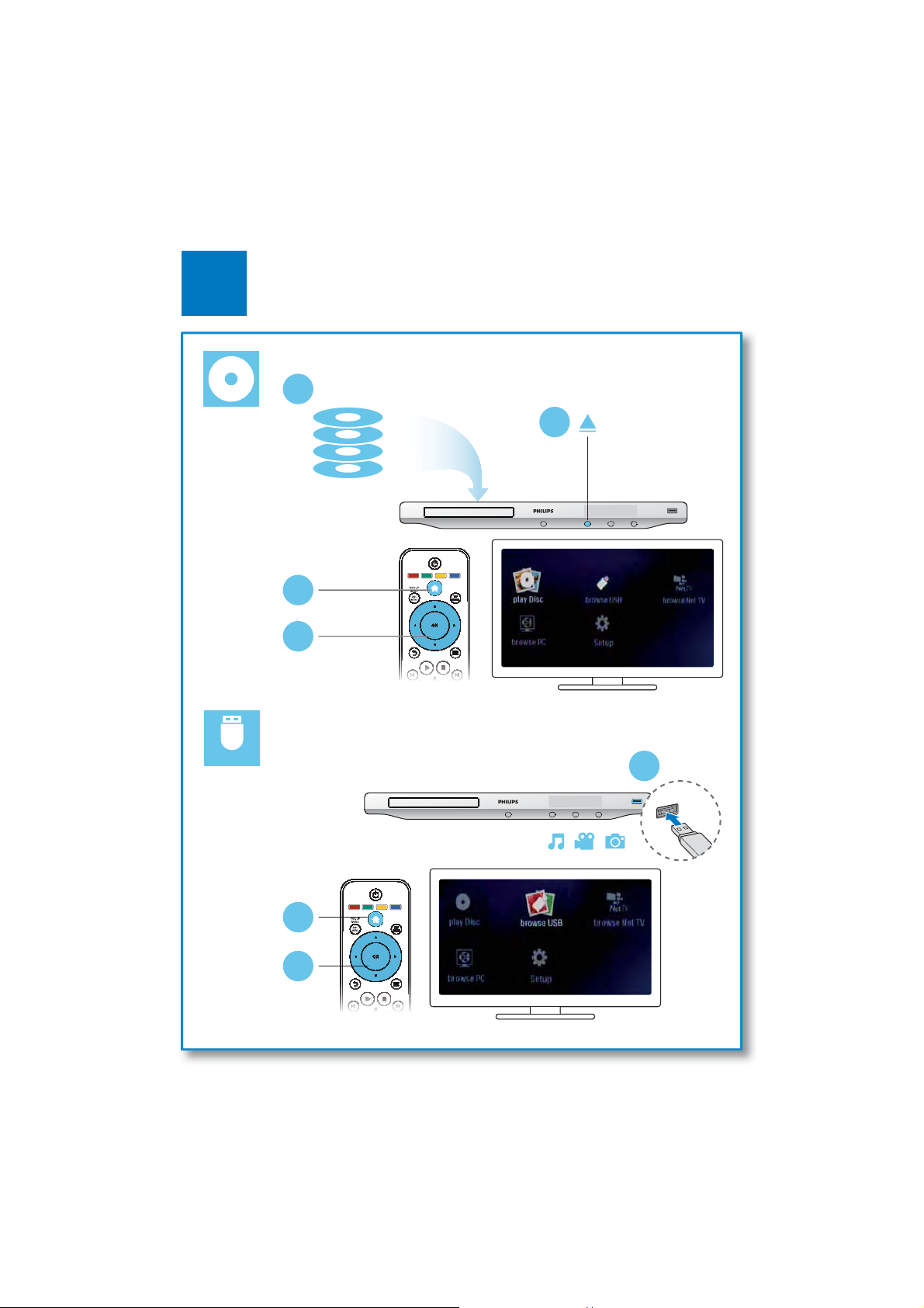
6
1-8
2
BD/BD 3D
DVD/VCD/CD
DivX Plus HD/MKV
MP3 / JPEG
1
3
4
USB
1
2
3
Page 10

1 -9
2. Safety Instructions, Warnings, Notes, and Abbreviation List
Index of this chapter:
2.1 Safety Instructions
2.2 Warnings
2.3 Notes
2.4 Abbreviation List
2.1 Safety Instructions
Safety regulations require the following during a repair:
• Connect the set to the Mains/AC Power via an isolation
transformer (> 800 VA).
• Replace safety components, indicated by the symbol
only by components identical to the original ones. Any
other component substitution (other than original type) may
increase risk of fire or electrical shock hazard.
Safety regulations require that after a repair, the set must be
returned in its original condition. Pay in particular attention to
the following points:
• Route the wire trees correctly and fix them with the
mounted cable clamps.
• Check the insulation of the Mains/AC Power lead for
external damage.
• Check the strain relief of the Mains/AC Power cord for
proper function.
• Check the electrical DC resistance between the Mains/AC
Power plug and the secondary side (only for sets that have
a Mains/AC Power isolated power supply):
1. Unplug the Mains/AC Power cord and connect a wire
between the two pins of the Mains/AC Power plug.
2. Set the Mains/AC Power switch to the “on” position
(keep the Mains/AC Power cord unplugged!).
3. Measure the resistance value between the pins of the
Mains/AC Power plug and the metal shielding of the
tuner or the aerial connection on the set. The reading
should be between 4.5 M: and 12 M:.
4. Switch “off” the set, and remove the wire between the
two pins of the Mains/AC Power plug.
• Check the cabinet for defects, to prevent touching of any
inner parts by the customer.
2.2 Warnings
• All ICs and many other semiconductors are susceptible to
electrostatic discharges (ESD ). Careless handling
during repair can reduce life drastically. Make sure that,
during repair, you are connected with the same potential as
the mass of the set by a wristband with resistance. Keep
components and tools also at this same potential.
• Be careful during measurements in the high voltage
section.
• Never replace modules or other components while the unit
is switched “on”.
• When you align the set, use plastic rather than metal tools.
This will prevent any short circuits and the danger of a
circuit becoming unstable.
2.3 Notes
2.3.1 General
• Measure the voltages and waveforms with regard to the
chassis (= tuner) ground ( ), or hot ground ( ), depending
on the tested area of circuitry. The voltages and waveforms
shown in the diagrams are indicative. Measure them in the
Service Default Mode (see chapter 5) with a colour bar
signal and stereo sound (L: 3 kHz, R: 1 kHz unless stated
otherwise) and picture carrier at 475.25 MHz for PAL, or
61.25 MHz for NTSC (channel 3).
• Where necessary, measure the waveforms and voltages
with ( ) and without ( ) aerial signal. Measure the
voltages in the power supply section both in normal
operation ( ) and in stand-by ( ). These values are
indicated by means of the appropriate symbols.
2.3.2 Schematic Notes
• All resistor values are in ohms, and the value multiplier is
often used to indicate the decimal point location (e.g. 2K2
indicates 2.2 k:).
,
• Resistor values with no multiplier may be indicated with
either an “E” or an “R” (e.g. 220E or 220R indicates 220 :).
• All capacitor values are given in micro-farads (P u10
nano-farads (n u10
• Capacitor values may also use the value multiplier as the
decimal point indication (e.g. 2p2 indicates 2.2 pF).
• An “asterisk” (*) indicates component usage varies. Refer
to the diversity tables for the correct values.
• The correct component values are listed in the Spare Parts
List. Therefore, always check this list when there is any
doubt.
2.3.3 BGA (Ball Grid Array) ICs
Introduction
For more information on how to handle BGA devices, visit this
URL: www.atyourservice.ce.philips.com (needs subscription,
not available for all regions). After login, select “Magazine”,
then go to “Repair downloads”. Here you will find Information
on how to deal with BGA-ICs.
BGA Temperature Profiles
For BGA-ICs, you must use the correct temperature-profile,
which is coupled to the 12NC. For an overview of these profiles,
visit the website www.atyourservice.ce.philips.com (needs
subscription, but is not available for all regions)
You will find this and more technical information within the
“Magazine”, chapter “Repair downloads”.
For additional questions please contact your local repair help
desk.
2.3.4 Lead-free Soldering
Due to lead-free technology some rules have to be respected
by the workshop during a repair:
• Use only lead-free soldering tin Philips SAC305 with order
code 0622 149 00106. If lead-free solder paste is required,
please contact the manufacturer of your soldering
equipment. In general, use of solder paste within
workshops should be avoided because paste is not easy to
store and to handle.
• Use only adequate solder tools applicable for lead-free
soldering tin. The solder tool must be able:
– To reach a solder-tip temperature of at least 400°C.
– To stabilize the adjusted temperature at the solder-tip.
– To exchange solder-tips for different applications.
• Adjust your solder tool so that a temperature of around
360°C - 380°C is reached and stabilized at the solder joint.
Heating time of the solder-joint should not exceed ~ 4 sec.
Avoid temperatures above 400°C, otherwise wear-out of
tips will increase drastically and flux-fluid will be destroyed.
To avoid wear-out of tips, switch “off” unused equipment or
reduce heat.
• Mix of lead-free soldering tin/parts with leaded soldering
tin/parts is possible but PHILIPS recommends strongly to
avoid mixed regimes. If this cannot be avoided, carefully
clear the solder-joint from old tin and re-solder with new tin.
-9
), or pico-farads (p u10
-6
),
-12
).
Page 11
Safety Instructions, Warnings, Notes, and Abbreviation List
2.3.5 Alternative BOM identification
1 - 10
2.4 Abbreviation List
It should be noted that on the European Service website,
“Alternative BOM” is referred to as “Design variant”.
The third digit in the serial number (example:
KX2B0835000001) indicates the number of the alternative
B.O.M. (Bill Of Materials) that has been used for producing the
specific AV set. In general, it is possible that the same AV
model on the market is produced with e.g. two different types
of display, coming from two different suppliers. This
will then result in sets which have the same CTN (Commercial
Type Number; e.g. MCM394/12) but which have a different
B.O.M. number.
Also, it is possible that same model on the market is produced
with two production centers, however their partslist is the same.
In such case, no alternative B.O.M. will be created.
By looking at the third digit of the serial number, one can
identify which B.O.M. is used for the set he is working with.
If the third digit of the serial number contains the number “1”
(example: KX 1B033500001), then the set has been
manufactured according to B.O.M. number 1. If the third digit is
a “2” (example: KX 2B0335000001), then the set has been
produced according to B.O.M. no. 2. This is important for
ordering the correct spare parts!
For the third digit, the numbers 1...9 and the characters A...Z
can be used, so in total: 9 plus 26= 35 different B.O.M.s can be
indicated by the third digit of the serial number.
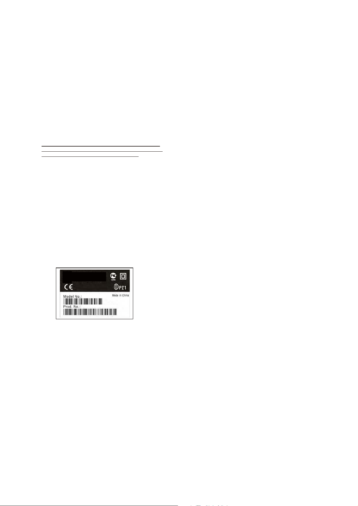
Identification: The bottom line of a type plate gives a 14-digit
serial number. Digits 1 and 2 refer to the production centre (e.g.
LM is Arts), digit 3 refers to the B.O.M. code, digit 4 refers
to the Service version change code, digits 5 and 6 refer to the
production year, and digits 7 and 8 refer to production week (in
example below it is 2008 week 50). The 6 last digits contain the
serial number.
Model FWM572/12
220-230 50Hz 60W
FWM572/12
LM1A0850005644
Figure 2-1 Serial number (example)
2.3.6 Module Level Repair (MLR) or Component Level Repair
(CLR)
If a board is defective, consult your repair procedure to decide
if the board has to be exchanged or if it should be repaired on
component level.
If your repair procedure says the board should be exchanged
completely, do not solder on the defective board. Otherwise, it
cannot be returned to the O.E.M. supplier for back charging!
2.3.7 Practical Service Precautions
• It makes sense to avoid exposure to electrical shock.
While some sources are expected to have a possible
dangerous impact, others of quite high potential are of
limited current and are sometimes held in less regard.
• Always respect voltages. While some may not be
dangerous in themselves, they can cause unexpected
reactions that are best avoided. Before reaching into a
powered TV set, it is best to test the high voltage insulation.
It is easy to do, and is a good service precaution.
0/6/12 SCART switch control signal on A/V
board. 0 = loop through (AUX to TV),
6 = play 16 : 9 format, 12 = play 4 : 3
format
2DNR Spatial (2D) Noise Reduction
3DNR Temporal (3D) Noise Reduction
AARA Automatic Aspect Ratio Adaptation:
algorithm that adapts aspect ratio to
remove horizontal black bars; keeps
the original aspect ratio
ACI Automatic Channel Installation:
algorithm that installs TV channels
directly from a cable network by
means of a predefined TXT page
ADC Analogue to Digital Converter
AFC Automatic Frequency Control: control
signal used to tune to the correct
frequency
AGC Automatic Gain Control: algorithm that
controls the video input of the feature
box
AM Amplitude Modulation
ANR Automatic Noise Reduction: one of the
algorithms of Auto TV
AP Asia Pacific
AR Aspect Ratio: 4 by 3 or 16 by 9
ASF Auto Screen Fit: algorithm that adapts
aspect ratio to remove horizontal black
bars without discarding video
information
ATSC Advanced Television Systems
Committee, the digital TV standard in
the USA
ATV See Auto TV
Auto TV A hardware and software control
system that measures picture content,
and adapts image parameters in a
dynamic way
AV External Audio Video
AVC Audio Video Controller
AVIP Audio Video Input Processor
B/G Monochrome TV system. Sound
carrier distance is 5.5 MHz
BLR Board-Level Repair
BTSC Broadcast Television Standard
Committee. Multiplex FM stereo sound
system, originating from the USA and
used e.g. in LATAM and AP-NTSC
countries
B-TXT Blue TeleteXT
C Centre channel (audio)
CEC Consumer Electronics Control bus:
remote control bus on HDMI
connections
CL Constant Level: audio output to
connect with an external amplifier
CLR Component Level Repair
COLUMBUS COlor LUMinance Baseband
Universal Sub-system
ComPair Computer aided rePair
CP Connected Planet / Copy Protection
CSM Customer Service Mode
CTI Color Transient Improvement:
manipulates steepness of chroma
transients
CVBS Composite Video Blanking and
Synchronization
DAC Digital to Analogue Converter
DBE Dynamic Bass Enhancement: extra
low frequency amplification
DDC See “E-DDC”
Page 12

1 - 11
Safety Instructions, Warnings, Notes, and Abbreviation List
D/K Monochrome TV system. Sound
carrier distance is 6.5 MHz
DFI Dynamic Frame Insertion
DFU Directions For Use: owner's manual
DMR Digital Media Reader: card reader
DMSD Digital Multi Standard Decoding
DNM Digital Natural Motion
DNR Digital Noise Reduction: noise
reduction feature of the set
DRAM Dynamic RAM
DRM Digital Rights Management
DSP Digital Signal Processing
DST Dealer Service Tool: special remote
control designed for service
technicians
DTCP Digital Transmission Content
Protection; A protocol for protecting
digital audio/video content that is
traversing a high speed serial bus,
such as IEEE-1394
DVB-C Digital Video Broadcast - Cable
DVB-T Digital Video Broadcast - Terrestrial
DVD Digital Versatile Disc
DVI(-d) Digital Visual Interface (d= digital only)
E-DDC Enhanced Display Data Channel
(VESA standard for communication
channel and display). Using E-DDC,
the video source can read the EDID
information form the display.
EDID Extended Display Identification Data
(VESA standard)
EEPROM Electrically Erasable and
Programmable Read Only Memory
EMI Electro Magnetic Interference
EPLD Erasable Programmable Logic Device
EU Europe
EXT EXTernal (source), entering the set by
SCART or by cinches (jacks)
FBL Fast BLanking: DC signal
accompanying RGB signals
FDS Full Dual Screen (same as FDW)
FDW Full Dual Window (same as FDS)
FLASH FLASH memory
FM Field Memory or Frequency
Modulation
FPGA Field-Programmable Gate Array
FTV Flat TeleVision
Gb/s Giga bits per second
G-TXT Green TeleteXT
H H_sync to the module
HD High Definition
HDD Hard Disk Drive
HDCP High-bandwidth Digital Content
Protection: A “key” encoded into the
HDMI/DVI signal that prevents video
data piracy. If a source is HDCP coded
and connected via HDMI/DVI without
the proper HDCP decoding, the
picture is put into a “snow vision” mode
or changed to a low resolution. For
normal content distribution the source
and the display device must be
enabled for HDCP “software key”
decoding.
HDMI High Definition Multimedia Interface
HP HeadPhone
dnuoS.metsysVTemorhconoMI
2
C Inter IC bus
I
2
I
D Inter IC Data bus
2
S Inter IC Sound bus
I
carrier distance is 6.0 MHz
IF Intermediate Frequency
Interlaced Scan mode where two fields are used
to form one frame. Each field contains
half the number of the total amount of
lines. The fields are written in “pairs”,
causing line flicker.
IR Infra Red
IRQ Interrupt Request
ITU-656 The ITU Radio communication Sector
(ITU-R) is a standards body
subcommittee of the International
Telecommunication Union relating to
radio communication. ITU-656 (a.k.a.
SDI), is a digitized video format used
for broadcast grade video.
Uncompressed digital component or
digital composite signals can be used.
The SDI signal is self-synchronizing,
uses 8 bit or 10 bit data words, and has
a maximum data rate of 270 Mbit/s,
with a minimum bandwidth of 135
MHz.
ITV Institutional TeleVision; TV sets for
hotels, hospitals etc.
JOP Jaguar Output Processor
LS Last Status; The settings last chosen
by the customer and read and stored
in RAM or in the NVM. They are called
at start-up of the set to configure it
according to the customer's
preferences
LATAM Latin America
LCD Liquid Crystal Display
LED Light Emitting Diode
L/L' Monochrome TV system. Sound
carrier distance is 6.5 MHz. L' is Band
I, L is all bands except for Band I
LORE LOcal REgression approximation
noise reduction
LPL LG.Philips LCD (supplier)
LS Loudspeaker
LVDS Low Voltage Differential Signalling
Mbps Mega bits per second
M/N Monochrome TV system. Sound
carrier distance is 4.5 MHz
MIPS Microprocessor without Interlocked
Pipeline-Stages; A RISC-based
microprocessor
MOP Matrix Output Processor
MOSFET Metal Oxide Silicon Field Effect
Transistor, switching device
MPEG Motion Pictures Experts Group
MPIF Multi Platform InterFace
MUTE MUTE Line
NC Not Connected
NICAM Near Instantaneous Compounded
Audio Multiplexing. This is a digital
sound system, mainly used in Europe.
NTC Negative Temperature Coefficient,
non-linear resistor
NTSC National Television Standard
Committee. Color system mainly used
in North America and Japan. Color
carrier NTSC M/N= 3.579545 MHz,
NTSC 4.43= 4.433619 MHz (this is a
VCR norm, it is not transmitted off-air)
NVM Non-Volatile Memory: IC containing
TV related data such as alignments
O/C Open Circuit
OSD On Screen Display
OTC On screen display Teletext and
Control; also called Artistic (SAA5800)
P50 Project 50: communication protocol
between TV and peripherals
PAL Phase Alternating Line. Color system
mainly used in West Europe (color
carrier= 4.433619 MHz) and South
America (color carrier PAL M=
Page 13

1 - 12
Safety Instructions, Warnings, Notes, and Abbreviation List
3.575612 MHz and PAL N= 3.582056
MHz)
PCB Printed Circuit Board (same as “PWB”)
PCM Pulse Code Modulation
PDP Plasma Display Panel
PFC Power Factor Corrector (or Pre-
conditioner)
PIP Picture In Picture
PLL Phase Locked Loop. Used for e.g.
FST tuning systems. The customer
can give directly the desired frequency
POR Power On Reset, signal to reset the uP
Progressive Scan Scan mode where all scan lines are
displayed in one frame at the same
time, creating a double vertical
resolution.
PTC Positive Temperature Coefficient,
non-linear resistor
PWB Printed Wiring Board (same as “PCB”)
PWM Pulse Width Modulation
QRC Quasi Resonant Converter
QTNR Quality Temporal Noise Reduction
QVCP Quality Video Composition Processor
RAM Random Access Memory
RGB Red, Green, and Blue. The primary
color signals for TV. By mixing levels
of R, G, and B, all colors (Y/C) are
reproduced.
RC Remote Control
RC5 / RC6 Signal protocol from the remote
control receiver
RESET RESET signal
ROM Read Only Memory
R-TXT Red TeleteXT
SAM Service Alignment Mode
S/C Short Circuit
SCART Syndicat des Constructeurs
d'Appareils Radiorécepteurs et
SCL Serial Clock I
Téléviseurs
SCL-F CLock Signal on Fast I
SD Standard Definition
SDA Serial Data I
SDA-F DAta Signal on Fast I
2
C
2
C bus
2
C
2
C bus
SDI Serial Digital Interface, see “ITU-656”
SDRAM Synchronous DRAM
SECAM SEequence Couleur Avec Mémoire.
Color system mainly used in France
and East Europe. Color carriers=
4.406250 MHz and 4.250000 MHz
SIF Sound Intermediate Frequency
SMPS Switched Mode Power Supply
SoC System on Chip
SOG Sync On Green
SOPS Self Oscillating Power Supply
S/PDIF Sony Philips Digital InterFace
SRAM Static RAM
SRP Service Reference Protocol
SSB Small Signal Board
STBY STand-BY
SVGA 800x600 (4:3)
SVHS Super Video Home System
SW Software
SWAN Spatial temporal Weighted Averaging
Noise reduction
SXGA 1280x1024
TFT Thin Film Transistor
THD Total Harmonic Distortion
TMDS Transmission Minimized Differential
Signalling
TXT TeleteXT
TXT-DW Dual Window with TeleteXT
UI User Interface
uP Microprocessor
UXGA 1600x1200 (4:3)
V V-sync to the module
VCR Video Cassette Recorder
VESA Video Electronics Standards
Association
VGA 640x480 (4:3)
VL Variable Level out: processed audio
output toward external amplifier
VSB Vestigial Side Band; modulation
method
WYSIWYR What You See Is What You Record:
record selection that follows main
picture and sound
WXGA 1280x768 (15:9)
XTAL Quartz crystal
XGA 1024x768 (4:3)
Y Luminance signal
Y/C Luminance (Y) and Chrominance (C)
signal
YPbPr Component video. Luminance and
scaled color difference signals (B-Y
and R-Y)
YUV Component video
Page 14

2-1
Mechanical and Dismantling Instructions
Dismantling Instruction
The following guidelines show how to dismantle the player.
Step1: Remove 6 screws around the Top Cover, and then remove the Top Cover (Figure 1).
Figure 1
Detailed information please refer to the model set.
Step2: If it is necessary to dismantle Loader or Front Panel, the Front door should be removed first. (Figure 2)
Note: Make sure to operate gently otherwise the guider would be damaged.
Please kindly note that dismantle the front door
assembly carefully to avoid damage tray and the front door.
Figure 2
Page 15

2-2
XP1
XP4
Mechanical and Dismantling Instructions
Detailed information please refer to the model set.
Dismantling Instruction
Step3: Dismantling Front Panel, disconnect the connectors (XP2, XP3,XP4)(Figure 6)
J3
J4
XP5
XP3
Step4: Dismantling Front Panel,
out from the set. (Figure 4 )
need release 2 snaps of Front Panel and 2 snaps of bottom cabinet , then gently pull the Panel
Figure 3
XP2
CN7
Figure 4
Page 16

2-3
Mechanical and Dismantling Instructions
Dismantling Instruction
Step5: Dismantling Loader, disconnect the 3 connectors (XP5, J3, J4)(Figure 3) aiming in the below figure, and remove 4 screws that
connects the loader and the bottom cabinet. (Figure 4-5)
Detailed information please refer to the model set.
Figure 5
Step6: Dismantling Main Board and AV Board, first disconnect the connector (XP4), and then remove 5 screws. (Figure 6)
Step7:Remove 3 screws on Power Board to dismantle the Power Board. (Figure 6)
Figure 6
Page 17

3-1
Software check and upgrade
Preparation to upgrade software
1)Start the USB burning software & create a folder named "UPG_ALL" B. Read out the software versions to confirm upgrading
2)Then copy the Bin file (BDP_5200.bin )into it,
3)Burn the data onto the blank USB. 1) Power on the set and open the tray door.
4)If the model is BDP5200,must use (BDP_5200.bin )to upgrade 2) Press <Home> button on the reomote control.
A. Procedure for software upgrade 3) Select <Setup>, then press <OK>.
A) Upgrade softwar via network:
4) Select <Advanced Setup>, press right cursor to choose
1) Setup the network connection (See "Getting started">"Set up
<Version Info.>, then press <OK>, the software version
network").
2) In the Home menu, select <Setting>-<Advanced Setup> Model:BDP5XXX/XX
<Software Download>-<Network>.
Versions:
* You are prompted to start upgrading processes if upgrade
media is detected.
http://www.philips.com/support
3) Follow the instructions on the TV screen to confirm update
operation.
* Once software updated is complete, this player automatically
truns off to standby.
4) Disconnect the power cord for a few seconds and connect again
to turn on the player.
Update software via USB Flash Drive:
B) Update software via USB Flash Drive:
1) Go to www.philips.com/support to check if the latest software
version is available for this player.
2) Download the software onto a USB flash drive.
3) Insert the USB flash drive to the USB jack of the rear panel.
4) In the Home menu, select <Setup>-<Advanced Setup>-<Software Updade
>-<USB>.
5) Follow the instructions on the TV screen to confrim update operation.
* Once software update is complete, this player automatically turns to
standby.
6) Disconnect the power cord for a few seconds and connect again to
turn on the player.
and other information will display on the TV screen as below:
MAC:XX-XX-XX-XX-XX-XX
Caution: The set must not be power off during
upgrading, otherwise the Main board will be
damaged entirely.
Page 18

4-1
No display on VFD, and buttons do not work
Trouble shooting chart
No display on VFD, and
buttons do not work
Yes
Check every supply voltage on
main board is
normal:XP4(PIN6:5V,PIN7:12V,
PIN10:-24V)
Yes
No
Refer to Power supply board part
Check the front board
signals(square-wave)VCLK,VD,
VSTB, (CN1:pin10,11,12),
No
Check the front board CN7’s pin
1,2,3 arrive the condition CN1’pin
Yes
1.Check the VFD board whether
bad solder exists on U2 and pins of
VFD
2.Check whether the circuit
connected to SW1, SW2, SW3,
SW4 are broken.
No
Correct connection
Yes
Replace U2 or VFD
Page 19

4-2
Trouble shooting chart
No audio output
No audio output
Yes
Check if CN7\CN8 conection
is ok or not pin to pin from the
AV board to mainboard
No
Fix CN7/CN8 from AV
board to mainboard
Yes
Check whether the audio signal is right
from the U15:’9pin and 10pin
(When you play 1KHz signal disk,the
output is about 2V sine wave)
Yes
Check If the R310,R311 are exsit
No
No
Check the U15 on power supply
(U15:11pin and 14pin=3.3V)
No
Replace the U15
Add the two Resistances
Page 20

Remote control does not work
Remote control
does not work
Yes
Check whether the remote
control’s battery is
exhausted or not.
Yes
Check if the ET3045 power
supply is OK,
˄PIN20 ˅is about 5V
Ye s
ET3045
4-3
Trouble shooting chart
No
Replace the battery for remote
No
Check the VCC net on front board
No
Replace ET3045
control
Page 21

Can’t read disc or can’t open the disk door
4-4
Trouble shooting chart
Can’t read disc or can’t
open the disk door
Yes
Check whether the DVD loader
running is normal(the OPU is
moving or eradiating the red lase)
NO
Check the connection
4pin cable from the
main board
Yes
Check 45pin and 9pin
cable from main board
connection to the loader is
normal
NO
Fix the connection the 45pin cable or
9pin cable.
Yes
Check if J3 (pin36) voltage
is normal (about 8V)
NO
Fix R212/R8213/U19 on the
main board
Yes
Check R217/R218/R219 are
normal (the resitance are
0 OHM or fixed well )
NO
Fix R217/R218/R219 on the
main board
Yes
Replace the loade
Page 22

)
4-5
Trouble shooting chart
No video display
No Video display
Yes
Check if CN7/CN8 fix well from
AV board to mainboard.(the
solder of CN7/CN8 is OK
Yes
Check if L452 is on main BD
Yes
No
Fix CN7,CN8 in AV board
No
Add L452
Check If R616 is
on
Main BD
No
Add R616
Replace the main board
Page 23

Can not connect to network
Can not connect to
network
Yes
Check if LFE8634(U14)
main board
is on
Yes
Check
R580,R133,R134,R560,R
579 is on main board
Yes
Change the P2 on the
main board(refer to schematic
of main board )
4-6
No
Fix U14 in main board
No
Fix all the resistor
Trouble shooting chart
Page 24

Can not connect to WIFI
Can not connect to
WIFI
Check XP3 (pin1)
voltage is normal(3.3V)
Check the connection
from wifi board to
mainboard
Change the wifi module
Yes
Yes
Yes
is fixed or not
4-7
No
No
Trouble shooting chart
Check the R965 is fixed on
Check the order of wifi
wire:from yellow\white\red
to yellow \white\red
No
Change the wifi wire
well
Page 25

5-1
5-1
A
B
C
D
E
BDP5200/12 /05/51/98/55/K93/X78 Block diagram:
1 1
HDMINET PORT
SD CARD
SMSC8710
Ethernet PHY
HDMI OUT
2 2
45PIN FCC
LOADER: L9829A
45 PIN9 PIN4PIN
J3
TRAY
TPC1391G4
WIFI signal
MT8555
OPU:SONY 470
TPIC1405A
9PIN FCC
J4XP5
4pin line
MOTOR DRIVER
WIFI signal
2Gb NFLASH
4PIN
USB signal
4PIN XP2
XP3
USB power
MAI BOARD
I2S OUT
1Gb DDR3
1333MHz
AK4430
1Gb DDR3
1.1V
1.5V
3.3V
COAXIAL
USB signal
1333MHz
G5693
G5693
G966A
CVBS OUT
1Gb DDR3
1333MHz
1Gb DDR3
1333MHz
G566B
L+R+CVBS
AV BOARD
USB power
POWER
control
circuit
6PIN XP1
-24V
+12V
AS117
AC IN
PSU
14PIN XP4
8V
6PIN CN7
3 3
POWER CONNECTOR
14 pin line
WIFI CONNECOTR
USB CONNECTOR
WIFI MODEL
14PIN
USB
MCU
KEY BOARD
VFD BOARD
6312
4 4
A
B
C
D
E
Page 26

5-2
5-2
A
BDP5200/12 /05/51/98/55/K93/X78 Wiring diagram:
1 1
LOADER :L9829A
2 2
B
45pin
SD CARD
FFC CABLE
NET PORT
SMSC8701
C
HDMI OUT
HDMI
COAXIAL CVBS L R
5
5
6
I2S OUT
13
642
1.MUTE
2.ROUT1
3.LOUT1
4.VCC_D
5.GND
6.SPDIF
1
234
L+R
AK4430
CVBS
AV BOARD
6
2
5
34
1
D
6
5
4
3
2
1
1.none
2.none
3.none
4.GND
5.GND
6.CVBS
AC~
E
OPU:SONY 470
MT8555
9pin
TPIC_LOADER-
TPIC_LOADER+
MGND
TRAYIN
3 3
TPC1391G4
FFC CABLE
1
234
WIFI PORT
WIFI DONGLE
TPIC1405A
FLASH
123
GND
123
4
USBP2
GND
USBM2
USB_VCC1(+3.3V)
G556B
4
USB
USBM1
USBP1
USB_VCC3(+5V)
1333M
1Gb DDR3
1333M
1Gb DDR3
1.1V
1.5V
3.3V
AS117
1Gb DDR3
1333M
1Gb DDR3
1333M
G5693
G5693
G966A
+12V+8V
POWER
CONTROL
1
23456
+5V
+5V
GND
CIRCUIT
GND
+12V
-24V
14
OPEN_K
13
IIC_INT_MCU
12
CEC
SDA
-24V_D(-22V~-24V)
SCL
8 91011
PCON
7
+12V_D(+12V)
VCC(+5V)
VDATA
VCLK
VSTB
23456
GND
1
IR
PSU
1
23456
+5V
+5V
GND
+12V
GND
-24V
4 4
1
2345678 91011
A
12
13
14
VFD
FK BOARD
B
C
MCU
POWER
432
USB
1
D
E
Page 27

6-1
6-1
A
B
C
D
E
KE Board Circuit Diagram:MCU
VCC3V3
CN4
CN4
1
2
3
1 1
VCC VCC3
FB1
FB1
FB60/1A
FB60/1A
C35
C35
0.1uF/50V/Y5V
0.1uF/50V/Y5V
10
R1310R13
R1410R14
D
Vin
13GS1206S-00BU213GS1206S-00B
CE9100uF/10V+CE9100uF/10V
S
U2
Vout
VSS
G
+
C36
C36
0.1uF/50V/Y5V
0.1uF/50V/Y5V
VCC3
10
VCC3V3
2 2
R151KR15
PCON
1K
4PIN/2.0mm/100mm
4PIN/2.0mm/100mm
VCC
R16
R16
470
470
Q6
Q6
NPN_3DG3904M
NPN_3DG3904M
4
Q7
Q7
PNP_3CG3906M
PNP_3CG3906M
VCC3V3
1
2
MODE
3
RST_MCU
4
VCC3V3
R64
R64
10K
10K
+
+
CE3
CE3
47uF/16V
47uF/16V
R76
R76
4.7K
4.7K
-24V_D
+5V
+12V_D
22uF/50V
CE4+22uF/50V
U1
U1
R5F211B4SP
R5F211B4SP
M_SCL M_SDA
R66 33R66 33
PCON
R65 33R65 33
C380.1uF/16V/Y5V C380.1uF/16V/Y5V
C3710uF/10V/Y5V C3710uF/10V/Y5V
VCC3
R80R8
R77 100R77 100
+5V
0
CEC_IN
CEC_OUT
1
P3_5/SSCK/SCL/CMP1_2
2
P3_7/CNTR0/SSO/TXD1
3
RESET
4
XOUT/P4_7
5
VSS/AVSS
6
XIN/P4_6
7
VCC/AVCC
8
MODE
9
P4_5/INTO/RXD1
10
P1_7/CNTR00/INT10
P3_4/SCS/SDA/CMP1_1
P3_3/TCIN/INT3/SS100/CMP1_0
P1_0/KI0/AN8/CMP0_0
P1_1/KI1/AN9/CMP0_1
P4_2/VREF
P1_2/KI2/AN10/CMP0_2
P1_3/KI3/AN11/TZOUT
P1_4/TXD0
P1_5/RXD0/CNTR01/INT11
P1_6/CLK0/SSIO1
20
19
18
17
16
15
14
13
12
11
R68 33R68 33
R62 470R62 470
R59 33R59 33
R63 33R63 33
R79 33R79 33
R69 33R69 33
R78 33/NCR78 33/NC
MCU_OUT1
POWER_KEY
EJECT
IR
PLAY
STOP
M_INT
R70 820R70 820
VCC3V3
LED1
LED1
RED LED02B
RED LED02B
CE4
+
STB
CLK
DATA
PLAY
STOP
POWER_KEY
EJECT
4PIN/2.54mm
4PIN/2.54mm
CN6
CN6
1
1
2
2
ᴰ䙺䩜
ᴰ䙺䩜
3
3
4
4
TO VFD PCB
TO VFD PCB
4PIN/2.54mm
4PIN/2.54mm
CN7
CN7
1
1
2
2
ᴰ䙺䩜
ᴰ䙺䩜
3
3
4
4
TO VFD PCB
TO VFD PCB
5
5
6
6
7
7
8
8
VCC3V3
L1 10uH/0.1AL1 10uH/0.1A
R74
R71
R71
18K
18K
CEC_IN
3 3
CEC_OUT
IR1
IR1
5
GND
4
GND
3
VCC
2
GND
IR
1
IR
IRM_12mm
4 4
IRM_12mm
C21
C21
47pF
47pF
C40
C40
220pF/50V/NP0/NC
220pF/50V/NP0/NC
R72 100KR72 100K
C22
C22
0.1uF
0.1uF
R57 100R57 100
+
+
CE8
CE8
47uF/10V
47uF/10V
R73 0R73 0
R74
C41
C41
27K
27K
0.1uF/16V/Y5V
0.1uF/16V/Y5V
D1
LL4148D1LL4148
VCC3V3
R88
R88
10K
10K
EJECT
SW3 TAC020SW3 TAC020
R10R1
0
TP1TP1
GND
GND
USB PORT FOR MAIN
R89
R89
10K
10K
PLAY POWER_KEY
SW2 TAC020SW2 TAC020
C50
C50
47pF
47pF
P1
GND_1
6
GND
5
D+_1
GND
VCC_1
USBP1USB
D-_1
C52
C52
47pF
47pF
4
3
2
1
USB_DP
R54
R54
10K
10K
SW4 TAC020SW4 TAC020
USB_DP
USB_DN
C34
C34
0.1uF
0.1uF
C49
C49
47pF
47pF
GND_U
USB_DP
1
2 3
ESD1
ESD1
PRTR5V0U2X
PRTR5V0U2X
R58
R58
10K
10K
STOP
SW1 TAC020SW1 TAC020
R91 0R91 0
4
USB_DN
VCC5V
USB_DN
C51
C51
47pF
47pF
4PIN/2.0mm/100mm
4PIN/2.0mm/100mm
1
2
3
4
VCC5V
CN3
CN3
1
2
3
4
Q1
3DG3904MQ13DG3904M
C19
C19
0.1uF
0.1uF
M_CEC
R75
R75
220
220
C39220pF/50V/NP0/NC C39220pF/50V/NP0/NC
VCC
VCC3V3
R55
R55
R56
R56
10K
10K
10K
10K
M_INT
MCU_OUT1
M_CEC
M_SDA
-24V_D
M_SCL
PCON
+12V_D
VCC
DATA
CLK
STB
IR
TO MAIN BOARD
R67
R67
R80
R80
10K
10K
10K
10K
1
1
2
2
3
3
4
4
5
5
6
6
7
7
8
8
9
9
10
10
11
11
12
12
13
13
14
14
CN1
CN1
14PIN/2.0mm
14PIN/2.0mm
A
B
C
D
E
Page 28

6-2 6-2
5
4
3
2
1
FE Board Circuit Diagram:VFD
D D
VFD1 VFDVFD1 VFD
+12V
R1
+5V
R4
10KR410K
Q3
3DG3904MQ33DG3904M
C3
R11 18KR11 18K
Q6
3DG3904MQ63DG3904M
C C
4PIN/2.54mm
4PIN/2.54mm
CN1
CN1
1
1
ᴰ䙺䩜
ᴰ䙺䩜
TO MCU PCB
TO MCU PCB
2
3
4
-24V
2
+5V
3
+12V
4
C7
1000pFC71000pF
R161KR16
1K
R181KR18
1K
B B
0.1uFC30.1uF
R12
R12
4.7K
4.7K
4PIN/2.54mm
4PIN/2.54mm
CN2
CN2
1
2
ᴰ䙺䩜
ᴰ䙺䩜
3
4
TO MCU PCB
TO MCU PCB
5
6
7
8
470R1470
2.2R32.2
C15
C15
1uF/50V/Y5V
1uF/50V/Y5V
R9
R3
STB
CLK
DATA
ZD1
ZD1
-24V
Q2
3DG3904MQ23DG3904M
R5
470R5470
Q4
3DG3904MQ43DG3904M
R17
R17
10K
10K
1
2
3
4
5
6
7
8
CLK
STB
KEY4
DATA
K1
COMMON
K3
K2
Q5
3CG3906MQ53CG3906M
470R9470
R8
BZX79C6V2
BZX79C6V2
+5V
R4433R44
R45 33R45 33
R4633R46
AC2
R14
R14
10K
10K
-24V
C2 1000pFC2 1000pF
330R8330
C12
C12
0.1uF
0.1uF
33
33
C16 27pFC16 27pF
R10
R10
C20
C20
1uF/50V/Y5V
1uF/50V/Y5V
R29
R29
10K
10K
C17 27pFC17 27pF
2.2
2.2
R30
R30
10K
10K
C18 27pFC18 27pF
AC1
C9 0.1uFC9 0.1uF
R27
R27
10K
10K
COMMON
NP3F22F2
1
R21
R21
51K
51K
K3
R56 10KR56 10K
K2
R55 10KR55 10K
K1
R53 10KR53 10K
R54 10KR54 10K
NP48G5P16P277G8P396G
34
35
36
37
38
39
40
41
42
43
44
P7154G16P817P918P10193G20P11212G22P1223P1324NC25P14261G27P1528NP
5G14P613P512P4
11
10
33
31
G632G5
G4
G3
G2
G1
VDD
CS16312
CS16312
LED4
LED3
U2
U2
LED2
LED1
GND
OSC
SW11SW22SW33SW44SDout5SDin6GND7SCLK8/CS9KEY110KEY2
27
23
26
VEE
SEG9
SEG1024SEG1125SEG12
SEG1328SEG1429SEG1530SEG16
SEG8
SEG7
SEG6/K6
SEG5/K5
SEG4/K4
SEG3/K3
SEG2/K2
SEG1/K1
VDD
KEY4
KEY3
11
R522.2K R522.2K
R512.2K R512.2K
F132F131NP
30
29
AC2
C4
1000pFC41000pF
22
21
20
19
18
17
16
15
14
+5V
13
12
R58 2.2KR58 2.2K
R502.2K R502.2K
KEY4
A A
5
4
3
2
1
Page 29

6-3
6-3
A
B
C
D
E
AV Board Circuit Diagram:
C620
C620
47pF/50V/NP0
47pF/50V/NP0
SPDIF
R616 0R616 0
+
+
CE606
CE606
NC/220uF/16V
NC/220uF/16V
PESD5V0S1BA/30K/35pF
PESD5V0S1BA/30K/35pF
Left (White)
Right (Red)
CVBS
J601
J601
RCA3
RCA3
CVBS (Yellow)
LOUT1
CVBSCVBSO
D607
D607
2 1
MUTE
MUTE
R168 2.2KR168 2.2K
R167 2.2KR167 2.2K
Q49
Q49
NPN_3DG3904M
NPN_3DG3904M
Q48
Q48
NPN_3DG3904M
NPN_3DG3904M
C628
C628
100pF/50V/NP0
100pF/50V/NP0
C629
C629
100pF/50V/NP0
100pF/50V/NP0
ROUT1
FB1
FB1
C613
ASPDIF
R609 180/1%R609 180/1%
R610
R610
100/1%
1 1
100/1%
FE_GND
C613
0.1uF/25V/Y5V
0.1uF/25V/Y5V
C615
C615
100pF/50V/NP0
100pF/50V/NP0
500/200mA
500/200mA
P1
1
2
3
RCA/2hP1RCA/2h
FE_GND
SPDIF OUTOUT
GND
ASPDIF
LOUT1
VCC
AMUTE
ROUT1
GND
CVBSO
2 2
GND
6
6
5
5
4
4
3
3
2
2
1
1
CN7
CN7
CON2.54-2X6
CON2.54-2X6
6
6
5
5
4
4
3
3
2
2
1
1
CN8
CN8
CON2.54-2X6
CON2.54-2X6
VIDEO
BUFFER
LOW
IMPEDANCE
L452 1.8uH/50mAL452 1.8uH/50mA
R615
R615
75/1%
75/1%
C621
C621
47pF/50V/NP0
47pF/50V/NP0
VIDEO OUTPUT
AV
VCC
MUTE
Q218
Q218
PNP_3CG3906M
PNP_3CG3906M
R617
R617
100K
100K
R618 1KR618 1K
AMUTE
R169 2.2KR169 2.2K
Q50
Q50
NPN_3DG3904M
NPN_3DG3904M
3 3
4 4
CONNECTOR
A
B
C
D
E
Page 30

6-4
6-4
A
B
C
D
E
Power Board circuit diagram:
L501 680uHL501 680uH
C501
C501
103/1KV
D501
D501
RL207
RL207
1 1
D502
D502
RL207
RL207
TR501
TR501
10D205
10D205
PASPAS
R501 1MR501 1M
2 2
NC
CY501
CY501
470PF/250Vac
470PF/250Vac
D503
D503
PASPAS
RL207
RL207
D504
D504
RL207
RL207
PASPAS
LF501
LF501
30mH
30mH
PASPAS
R502 1MR502 1M
PASPAS
CX501 0.1UF/250VCX501 0.1UF/250V
PASPAS
PASPAS
CY502
CY502
470PF/250Vac
470PF/250Vac
PASPAS
CE501
CE501
+
+
22uF/400V
22uF/400V
PASPAS
CE502
CE502
+
+
22uF/400V
22uF/400V
CE503
CE503
+
+
22uF/400V
22uF/400V
S8550
S8550
Q501
Q501
U501
U501
TNY179P
TNY179P
5
6
7
8
Q502
Q502
S8550
S8550
R505A
R505A
150K
150K
S
S
S
S
R509
R509
R505B
R505B
150K
150K
Drain
NC
BP/M
EN/UV
D507
D507
1N4148
1N4148
2.2M 1206
2.2M 1206
R505C
R505C
150K
150K
4
3
2
1
C5020.47uF/63V C5020.47uF/63V
R505D
R505D
150K
150K
R5220R522
103/1KV
D505
D505
CE505
CE505
+
+
10UF/16V
10UF/16V
0
CY503 470PF/250VacCY503 470PF/250Vac
R50622R506
22
FR107
FR107
R507 390R507 390
R508 10kR508 10k
CY504
CY504
NC
ZD502
ZD502
11V 1/2W
11V 1/2W
D506 FR107D506 FR107
CE504
CE504
+
+
47UF/35V
47UF/35V
5
1
3
2
4
PASPAS
470PF/250Vac
470PF/250Vac
T501
T501
EF25
EF25
PASPAS
PASPAS
R514 47RR514 47R
9
7
8
10
6
D509
D509
SR360
SR360
8
R511 470RR511 470R
C503 102/100VC503 102/100V
D511 HER203D511 HER203
D508 FR107D508 FR107
D510
D510
SR360
SR360
C504
C504
222/50V
222/50V
R51322R513
22
R512
R512
CE509
CE509
+
+
2200uF/16V
2200uF/16V
L503 100/A05L503 100/A05
CE506
CE506
+
+
1000uF/25V
1000uF/25V
CE508
CE508
+
+
47uF/50V/85°
47uF/50V/85°
L502
L502
6.8uH
6.8uH
R515
R515
390
390
CE510
CE510
+
+
1000uF/16V
1000uF/16V
CE507
CE507
+
+
470uF/35V
470uF/35V
R517NCR517
NC
R518
R518
2.49k 1%
2.49k 1%
R521
R521
150
150
6
5
4
3
2
1
-24V
GND
+12V
GND
+5V
+5V
CN503
CN503
6PIN/2.5MM
6PIN/2.5MM
ZD501
RV501 10K471RV501 10K471
F501
F501
N1L
CN502
CN502
+1+
CN501NCCN501
NC
2
2
PASPAS
PASPAS
T2AL/250Vac
T2AL/250Vac
3 3
AC INPUT
AC INPUT
R503 1MR503 1M
PASPAS
R504 1MR504 1M
ZD501
11V /0.5W
11V /0.5W
12
43
U502
U502
PC123X
PC123X
2.2k
2.2k
3
U503
U503
2
TL431
TL431
1
C505 0.1uFC505 0.1uF
R516 1.2kR516 1.2k
R519
R519
2.4k 1%
2.4k 1%
R520NCR520
NC
NU:NO USE THE PLACE
* CAUTION :
4 4
THE PARTS MARKED WITH ARE IMPORTANT PARTS ON THE SAFETY.
PLEASE USE THE PARTS HAVING THE DESIGNATED PARTS NUMBER WITHOUT FAIL.
PASPAS
A
B
C
D
E
Page 31

6-5
6-5
FE Board Print-layout (Top and Bottom side):
Page 32

6-6
6-6
FK Board Print-layout (Bottom side):
Page 33

6-7
6-7
AV Board Print-layout (Bottom side):
Page 34

6-8
6-8
Power Board Print-layout (Bottom side):
Page 35

6-9
6-9
Main Board Print-layout (Top side):
Page 36

6-10
6-10
Main Board Print-layout (Bottom side):
Page 37

Exploded view for BDP5200/12/05/51/98/55/X78:
7-1
It is a general mechanical exploded view for BDP5200/12/05/51/98/55, pls refer to the model
set for detailed information.ASSY1 includes components:14.13.15.16.17.18.19.20.21
Page 38

Exploded view for BDP5200K/93:
7-2
Page 39

REVISION LIST
Version 1.0
* Initial release for BDP5200/12/05
Version 1.1
* Initial release for BDP5200/51/98
8-1
Version 1.
* Initial release for BDP5200/55
Version 1.
* Initial release for BDP5200/K93/X78
2
3
 Loading...