

Page 1
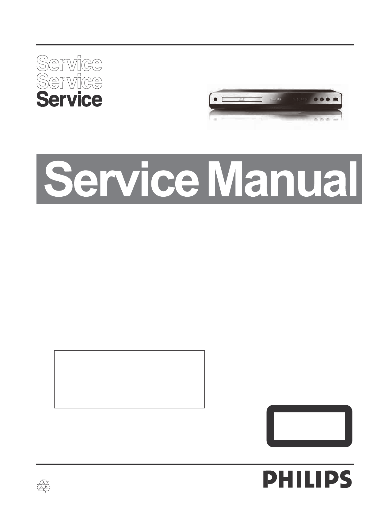
Blu-ray Disc Player
©
Second Generation
BDP3100/12/05/51/55/79/93/96/98/X78
BDP3080/98
TABLE OF CONTENTS
Technical Specifi cations .......................................................1-2
Safety Instruction, Warning & Notes .....................................1-3
PCBs Location, Version Variations.......................................1-7
Mechanical and Dismantling Instructions ................................2
Software Version & Upgrades, Region Code Change .............3
Trouble Shooting Chart ...........................................................4
Set Wiring Diagram .................................................................5
Electrical Diagrams and PCB layouts ......................................6
Set Mechanical Exploded view & Parts List ............................7
Revision List ............................................................................8
This service manual is for BDP3100 & BDP3080
Second Generation
previous generation model.
For Second Generation model, the serial number begins
with KX 2A(B,C,...) xxxxxxxxxx.
( Chipset Type: MT8550FBAG)
model, which is different from the
Page
©
Copyright 2010 Philips Consumer Electronics B.V. Eindhoven, The Netherlands
All rights reserved. No part of this publication may be reproduced, stored in a retrieval system or
transmitted, in any form or by any means, electronic, mechanical, photocopying, or otherwise without
the prior permission of Philips.
Version 1.2
CLASS 1
LASER PRODUCT
3141 785 35462GB
Page 2

1 - 2
1. Technical Specifications, Directions for Use
Index of this chapter:
1.1 Technical Specifications
1.2 Directions for Use
Notes:
• Figures can deviate due to the different set executions.
• Specifications are indicative (subject to change).
1.1 Technical Specifications
For on-line product support please use the following website:
http://www.p4c.philips.com/cgi-bin/dcbint/cpproduct_selector.pl
Here is product information available, as well as getting started,
user manuals, frequently asked questions and software &
drivers.
1.2 Directions for Use
You can download this information from the following websites:
http://www.philips.com/support
http://www.p4c.philips.com
Page 3

1 - 3
2. Safety Instructions, Warnings, Notes, and Abbreviation List
Index of this chapter:
2.1 Safety Instructions
2.2 Warnings
2.3 Notes
2.4 Abbreviation List
2.1 Safety Instructions
Safety regulations require the following during a repair:
• Connect the set to the Mains/AC Power via an isolation
transformer (> 800 VA).
• Replace safety components, indicated by the symbol
only by components identical to the original ones. Any
other component substitution (other than original type) may
increase risk of fire or electrical shock hazard.
Safety regulations require that after a repair, the set must be
returned in its original condition. Pay in particular attention to
the following points:
• Route the wire trees correctly and fix them with the
mounted cable clamps.
• Check the insulation of the Mains/AC Power lead for
external damage.
• Check the strain relief of the Mains/AC Power cord for
proper function.
• Check the electrical DC resistance between the Mains/AC
Power plug and the secondary side (only for sets that have
a Mains/AC Power isolated power supply):
1. Unplug the Mains/AC Power cord and connect a wire
between the two pins of the Mains/AC Power plug.
2. Set the Mains/AC Power switch to the “on” position
(keep the Mains/AC Power cord unplugged!).
3. Measure the resistance value between the pins of the
Mains/AC Power plug and the metal shielding of the
tuner or the aerial connection on the set. The reading
should be between 4.5 M: and 12 M:.
4. Switch “off” the set, and remove the wire between the
two pins of the Mains/AC Power plug.
• Check the cabinet for defects, to prevent touching of any
inner parts by the customer.
2.2 Warnings
• All ICs and many other semiconductors are susceptible to
electrostatic discharges (ESD ). Careless handling
during repair can reduce life drastically. Make sure that,
during repair, you are connected with the same potential as
the mass of the set by a wristband with resistance. Keep
components and tools also at this same potential.
• Be careful during measurements in the high voltage
section.
• Never replace modules or other components while the unit
is switched “on”.
• When you align the set, use plastic rather than metal tools.
This will prevent any short circuits and the danger of a
circuit becoming unstable.
2.3 Notes
2.3.1 General
• Measure the voltages and waveforms with regard to the
chassis (= tuner) ground ( ), or hot ground ( ), depending
on the tested area of circuitry. The voltages and waveforms
shown in the diagrams are indicative. Measure them in the
Service Default Mode (see chapter 5) with a colour bar
signal and stereo sound (L: 3 kHz, R: 1 kHz unless stated
otherwise) and picture carrier at 475.25 MHz for PAL, or
61.25 MHz for NTSC (channel 3).
• Where necessary, measure the waveforms and voltages
with ( ) and without ( ) aerial signal. Measure the
voltages in the power supply section both in normal
operation ( ) and in stand-by ( ). These values are
indicated by means of the appropriate symbols.
2.3.2 Schematic Notes
• All resistor values are in ohms, and the value multiplier is
often used to indicate the decimal point location (e.g. 2K2
indicates 2.2 k:).
,
• Resistor values with no multiplier may be indicated with
either an “E” or an “R” (e.g. 220E or 220R indicates 220 :).
• All capacitor values are given in micro-farads (P u10
nano-farads (n u10
• Capacitor values may also use the value multiplier as the
decimal point indication (e.g. 2p2 indicates 2.2 pF).
• An “asterisk” (*) indicates component usage varies. Refer
to the diversity tables for the correct values.
• The correct component values are listed in the Spare Parts
List. Therefore, always check this list when there is any
doubt.
2.3.3 BGA (Ball Grid Array) ICs
Introduction
For more information on how to handle BGA devices, visit this
URL: www.atyourservice.ce.philips.com (needs subscription,
not available for all regions). After login, select “Magazine”,
then go to “Repair downloads”. Here you will find Information
on how to deal with BGA-ICs.
BGA Temperature Profiles
For BGA-ICs, you must use the correct temperature-profile,
which is coupled to the 12NC. For an overview of these profiles,
visit the website www.atyourservice.ce.philips.com (needs
subscription, but is not available for all regions)
You will find this and more technical information within the
“Magazine”, chapter “Repair downloads”.
For additional questions please contact your local repair help
desk.
2.3.4 Lead-free Soldering
Due to lead-free technology some rules have to be respected
by the workshop during a repair:
• Use only lead-free soldering tin Philips SAC305 with order
code 0622 149 00106. If lead-free solder paste is required,
please contact the manufacturer of your soldering
equipment. In general, use of solder paste within
workshops should be avoided because paste is not easy to
store and to handle.
• Use only adequate solder tools applicable for lead-free
soldering tin. The solder tool must be able:
– To reach a solder-tip temperature of at least 400°C.
– To stabilize the adjusted temperature at the solder-tip.
– To exchange solder-tips for different applications.
• Adjust your solder tool so that a temperature of around
360°C - 380°C is reached and stabilized at the solder joint.
Heating time of the solder-joint should not exceed ~ 4 sec.
Avoid temperatures above 400°C, otherwise wear-out of
tips will increase drastically and flux-fluid will be destroyed.
To avoid wear-out of tips, switch “off” unused equipment or
reduce heat.
• Mix of lead-free soldering tin/parts with leaded soldering
tin/parts is possible but PHILIPS recommends strongly to
avoid mixed regimes. If this cannot be avoided, carefully
clear the solder-joint from old tin and re-solder with new tin.
-9
), or pico-farads (p u10
-12
-6
),
).
Page 4
Safety Instructions, Warnings, Notes, and Abbreviation List
2.3.5 Alternative BOM identification
1 - 4
2.4 Abbreviation List
It should be noted that on the European Service website,
“Alternative BOM” is referred to as “Design variant”.
The third digit in the serial number (example:
KX2B0835000001) indicates the number of the alternative
B.O.M. (Bill Of Materials) that has been used for producing the
specific AV set. In general, it is possible that the same AV
model on the market is produced with e.g. two different types
of display, coming from two different suppliers. This
will then result in sets which have the same CTN (Commercial
Type Number; e.g. MCM394/12) but which have a different
B.O.M. number.
Also, it is possible that same model on the market is produced
with two production centers, however their partslist is the same.
In such case, no alternative B.O.M. will be created.
By looking at the third digit of the serial number, one can
identify which B.O.M. is used for the set he is working with.
If the third digit of the serial number contains the number “1”
(example: KX1B033500001), then the set has been
manufactured according to B.O.M. number 1. If the third digit is
a “2” (example: KX2B0335000001), then the set has been
produced according to B.O.M. no. 2. This is important for
ordering the correct spare parts!
For the third digit, the numbers 1...9 and the characters A...Z
can be used, so in total: 9 plus 26= 35 different B.O.M.s can be
indicated by the third digit of the serial number.
Identification: The bottom line of a type plate gives a 14-digit
serial number. Digits 1 and 2 refer to the production centre (e.g.
LM is Arts), digit 3 refers to the B.O.M. code, digit 4 refers
to the Service version change code, digits 5 and 6 refer to the
production year, and digits 7 and 8 refer to production week (in
example below it is 2008 week 50). The 6 last digits contain the
serial number.
Model FWM572/12
220-230 50Hz 60W
FWM572/12
LM1A0850005644
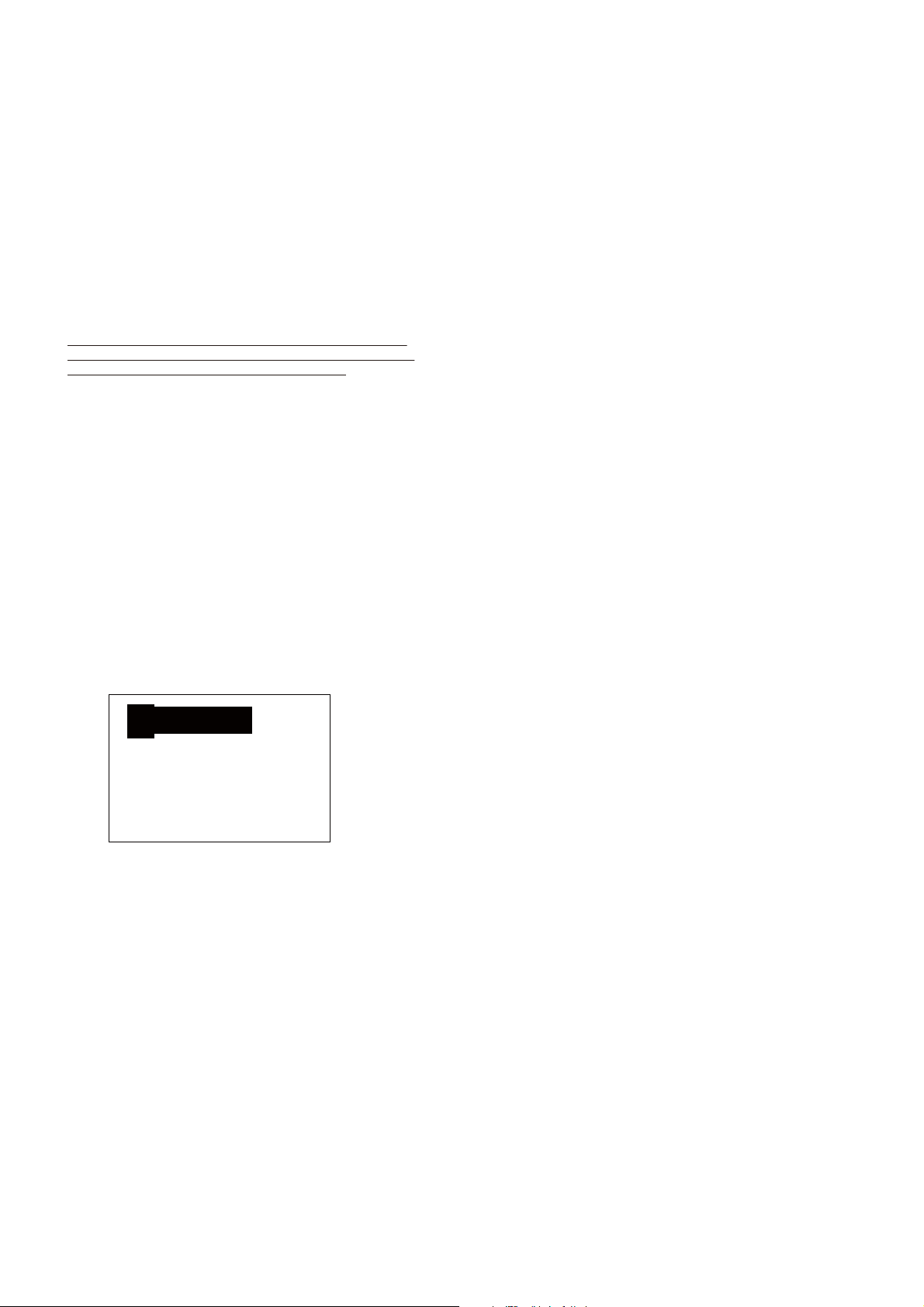
Figure 2-1 Serial number (example)
2.3.6 Module Level Repair (MLR) or Component Level Repair
(CLR)
If a board is defective, consult your repair procedure to decide
if the board has to be exchanged or if it should be repaired on
component level.
If your repair procedure says the board should be exchanged
completely, do not solder on the defective board. Otherwise, it
cannot be returned to the O.E.M. supplier for back charging!
2.3.7 Practical Service Precautions
• It makes sense to avoid exposure to electrical shock.
While some sources are expected to have a possible
dangerous impact, others of quite high potential are of
limited current and are sometimes held in less regard.
• Always respect voltages. While some may not be
dangerous in themselves, they can cause unexpected
reactions that are best avoided. Before reaching into a
powered TV set, it is best to test the high voltage insulation.
It is easy to do, and is a good service precaution.
0/6/12 SCART switch control signal on A/V
board. 0 = loop through (AUX to TV),
6 = play 16 : 9 format, 12 = play 4 : 3
format
2DNR Spatial (2D) Noise Reduction
3DNR Temporal (3D) Noise Reduction
AARA Automatic Aspect Ratio Adaptation:
algorithm that adapts aspect ratio to
remove horizontal black bars; keeps
the original aspect ratio
ACI Automatic Channel Installation:
algorithm that installs TV channels
directly from a cable network by
means of a predefined TXT page
ADC Analogue to Digital Converter
AFC Automatic Frequency Control: control
signal used to tune to the correct
frequency
AGC Automatic Gain Control: algorithm that
controls the video input of the feature
box
AM Amplitude Modulation
ANR Automatic Noise Reduction: one of the
algorithms of Auto TV
AP Asia Pacific
AR Aspect Ratio: 4 by 3 or 16 by 9
ASF Auto Screen Fit: algorithm that adapts
aspect ratio to remove horizontal black
bars without discarding video
information
ATSC Advanced Television Systems
Committee, the digital TV standard in
the USA
ATV See Auto TV
Auto TV A hardware and software control
system that measures picture content,
and adapts image parameters in a
dynamic way
AV External Audio Video
AVC Audio Video Controller
AVIP Audio Video Input Processor
B/G Monochrome TV system. Sound
carrier distance is 5.5 MHz
BLR Board-Level Repair
BTSC Broadcast Television Standard
Committee. Multiplex FM stereo sound
system, originating from the USA and
used e.g. in LATAM and AP-NTSC
countries
B-TXT Blue TeleteXT
C Centre channel (audio)
CEC Consumer Electronics Control bus:
remote control bus on HDMI
connections
CL Constant Level: audio output to
connect with an external amplifier
CLR Component Level Repair
COLUMBUS COlor LUMinance Baseband
Universal Sub-system
ComPair Computer aided rePair
CP Connected Planet / Copy Protection
CSM Customer Service Mode
CTI Color Transient Improvement:
manipulates steepness of chroma
transients
CVBS Composite Video Blanking and
Synchronization
DAC Digital to Analogue Converter
DBE Dynamic Bass Enhancement: extra
low frequency amplification
DDC See “E-DDC”
Page 5

1 - 5
Safety Instructions, Warnings, Notes, and Abbreviation List
D/K Monochrome TV system. Sound
carrier distance is 6.5 MHz
DFI Dynamic Frame Insertion
DFU Directions For Use: owner's manual
DMR Digital Media Reader: card reader
DMSD Digital Multi Standard Decoding
DNM Digital Natural Motion
DNR Digital Noise Reduction: noise
reduction feature of the set
DRAM Dynamic RAM
DRM Digital Rights Management
DSP Digital Signal Processing
DST Dealer Service Tool: special remote
control designed for service
technicians
DTCP Digital Transmission Content
Protection; A protocol for protecting
digital audio/video content that is
traversing a high speed serial bus,
such as IEEE-1394
DVB-C Digital Video Broadcast - Cable
DVB-T Digital Video Broadcast - Terrestrial
DVD Digital Versatile Disc
DVI(-d) Digital Visual Interface (d= digital only)
E-DDC Enhanced Display Data Channel
(VESA standard for communication
channel and display). Using E-DDC,
the video source can read the EDID
information form the display.
EDID Extended Display Identification Data
(VESA standard)
EEPROM Electrically Erasable and
Programmable Read Only Memory
EMI Electro Magnetic Interference
EPLD Erasable Programmable Logic Device
EU Europe
EXT EXTernal (source), entering the set by
SCART or by cinches (jacks)
FBL Fast BLanking: DC signal
accompanying RGB signals
FDS Full Dual Screen (same as FDW)
FDW Full Dual Window (same as FDS)
FLASH FLASH memory
FM Field Memory or Frequency
Modulation
FPGA Field-Programmable Gate Array
FTV Flat TeleVision
Gb/s Giga bits per second
G-TXT Green TeleteXT
H H_sync to the module
HD High Definition
HDD Hard Disk Drive
HDCP High-bandwidth Digital Content
Protection: A “key” encoded into the
HDMI/DVI signal that prevents video
data piracy. If a source is HDCP coded
and connected via HDMI/DVI without
the proper HDCP decoding, the
picture is put into a “snow vision” mode
or changed to a low resolution. For
normal content distribution the source
and the display device must be
enabled for HDCP “software key”
decoding.
HDMI High Definition Multimedia Interface
HP HeadPhone
dnuoS.metsysVTemorhconoMI
2
C Inter IC bus
I
2
I
D Inter IC Data bus
2
I
S Inter IC Sound bus
carrier distance is 6.0 MHz
IF Intermediate Frequency
Interlaced Scan mode where two fields are used
to form one frame. Each field contains
half the number of the total amount of
lines. The fields are written in “pairs”,
causing line flicker.
IR Infra Red
IRQ Interrupt Request
ITU-656 The ITU Radio communication Sector
(ITU-R) is a standards body
subcommittee of the International
Telecommunication Union relating to
radio communication. ITU-656 (a.k.a.
SDI), is a digitized video format used
for broadcast grade video.
Uncompressed digital component or
digital composite signals can be used.
The SDI signal is self-synchronizing,
uses 8 bit or 10 bit data words, and has
a maximum data rate of 270 Mbit/s,
with a minimum bandwidth of 135
MHz.
ITV Institutional TeleVision; TV sets for
hotels, hospitals etc.
JOP Jaguar Output Processor
LS Last Status; The settings last chosen
by the customer and read and stored
in RAM or in the NVM. They are called
at start-up of the set to configure it
according to the customer's
preferences
LATAM Latin America
LCD Liquid Crystal Display
LED Light Emitting Diode
L/L' Monochrome TV system. Sound
carrier distance is 6.5 MHz. L' is Band
I, L is all bands except for Band I
LORE LOcal REgression approximation
noise reduction
LPL LG.Philips LCD (supplier)
LS Loudspeaker
LVDS Low Voltage Differential Signalling
Mbps Mega bits per second
M/N Monochrome TV system. Sound
carrier distance is 4.5 MHz
MIPS Microprocessor without Interlocked
Pipeline-Stages; A RISC-based
microprocessor
MOP Matrix Output Processor
MOSFET Metal Oxide Silicon Field Effect
Transistor, switching device
MPEG Motion Pictures Experts Group
MPIF Multi Platform InterFace
MUTE MUTE Line
NC Not Connected
NICAM Near Instantaneous Compounded
Audio Multiplexing. This is a digital
sound system, mainly used in Europe.
NTC Negative Temperature Coefficient,
non-linear resistor
NTSC National Television Standard
Committee. Color system mainly used
in North America and Japan. Color
carrier NTSC M/N= 3.579545 MHz,
NTSC 4.43= 4.433619 MHz (this is a
VCR norm, it is not transmitted off-air)
NVM Non-Volatile Memory: IC containing
TV related data such as alignments
O/C Open Circuit
OSD On Screen Display
OTC On screen display Teletext and
Control; also called Artistic (SAA5800)
P50 Project 50: communication protocol
between TV and peripherals
PAL Phase Alternating Line. Color system
mainly used in West Europe (color
carrier= 4.433619 MHz) and South
America (color carrier PAL M=
Page 6

1 - 6
Safety Instructions, Warnings, Notes, and Abbreviation List
3.575612 MHz and PAL N= 3.582056
MHz)
PCB Printed Circuit Board (same as “PWB”)
PCM Pulse Code Modulation
PDP Plasma Display Panel
PFC Power Factor Corrector (or Pre-
conditioner)
PIP Picture In Picture
PLL Phase Locked Loop. Used for e.g.
FST tuning systems. The customer
can give directly the desired frequency
POR Power On Reset, signal to reset the uP
Progressive Scan Scan mode where all scan lines are
displayed in one frame at the same
time, creating a double vertical
resolution.
PTC Positive Temperature Coefficient,
non-linear resistor
PWB Printed Wiring Board (same as “PCB”)
PWM Pulse Width Modulation
QRC Quasi Resonant Converter
QTNR Quality Temporal Noise Reduction
QVCP Quality Video Composition Processor
RAM Random Access Memory
RGB Red, Green, and Blue. The primary
color signals for TV. By mixing levels
of R, G, and B, all colors (Y/C) are
reproduced.
RC Remote Control
RC5 / RC6 Signal protocol from the remote
control receiver
RESET RESET signal
ROM Read Only Memory
R-TXT Red TeleteXT
SAM Service Alignment Mode
S/C Short Circuit
SCART Syndicat des Constructeurs
d'Appareils Radiorécepteurs et
SCL Serial Clock I
Téléviseurs
SCL-F CLock Signal on Fast I
SD Standard Definition
SDA Serial Data I
SDA-F DAta Signal on Fast I
2
C
2
C bus
2
C
2
C bus
SDI Serial Digital Interface, see “ITU-656”
SDRAM Synchronous DRAM
SECAM SEequence Couleur Avec Mémoire.
Color system mainly used in France
and East Europe. Color carriers=
4.406250 MHz and 4.250000 MHz
SIF Sound Intermediate Frequency
SMPS Switched Mode Power Supply
SoC System on Chip
SOG Sync On Green
SOPS Self Oscillating Power Supply
S/PDIF Sony Philips Digital InterFace
SRAM Static RAM
SRP Service Reference Protocol
SSB Small Signal Board
STBY STand-BY
SVGA 800x600 (4:3)
SVHS Super Video Home System
SW Software
SWAN Spatial temporal Weighted Averaging
Noise reduction
SXGA 1280x1024
TFT Thin Film Transistor
THD Total Harmonic Distortion
TMDS Transmission Minimized Differential
Signalling
TXT TeleteXT
TXT-DW Dual Window with TeleteXT
UI User Interface
uP Microprocessor
UXGA 1600x1200 (4:3)
V V-sync to the module
VCR Video Cassette Recorder
VESA Video Electronics Standards
Association
VGA 640x480 (4:3)
VL Variable Level out: processed audio
output toward external amplifier
VSB Vestigial Side Band; modulation
method
WYSIWYR What You See Is What You Record:
record selection that follows main
picture and sound
WXGA 1280x768 (15:9)
XTAL Quartz crystal
XGA 1024x768 (4:3)
Y Luminance signal
Y/C Luminance (Y) and Chrominance (C)
signal
YPbPr Component video. Luminance and
scaled color difference signals (B-Y
and R-Y)
YUV Component video
Page 7
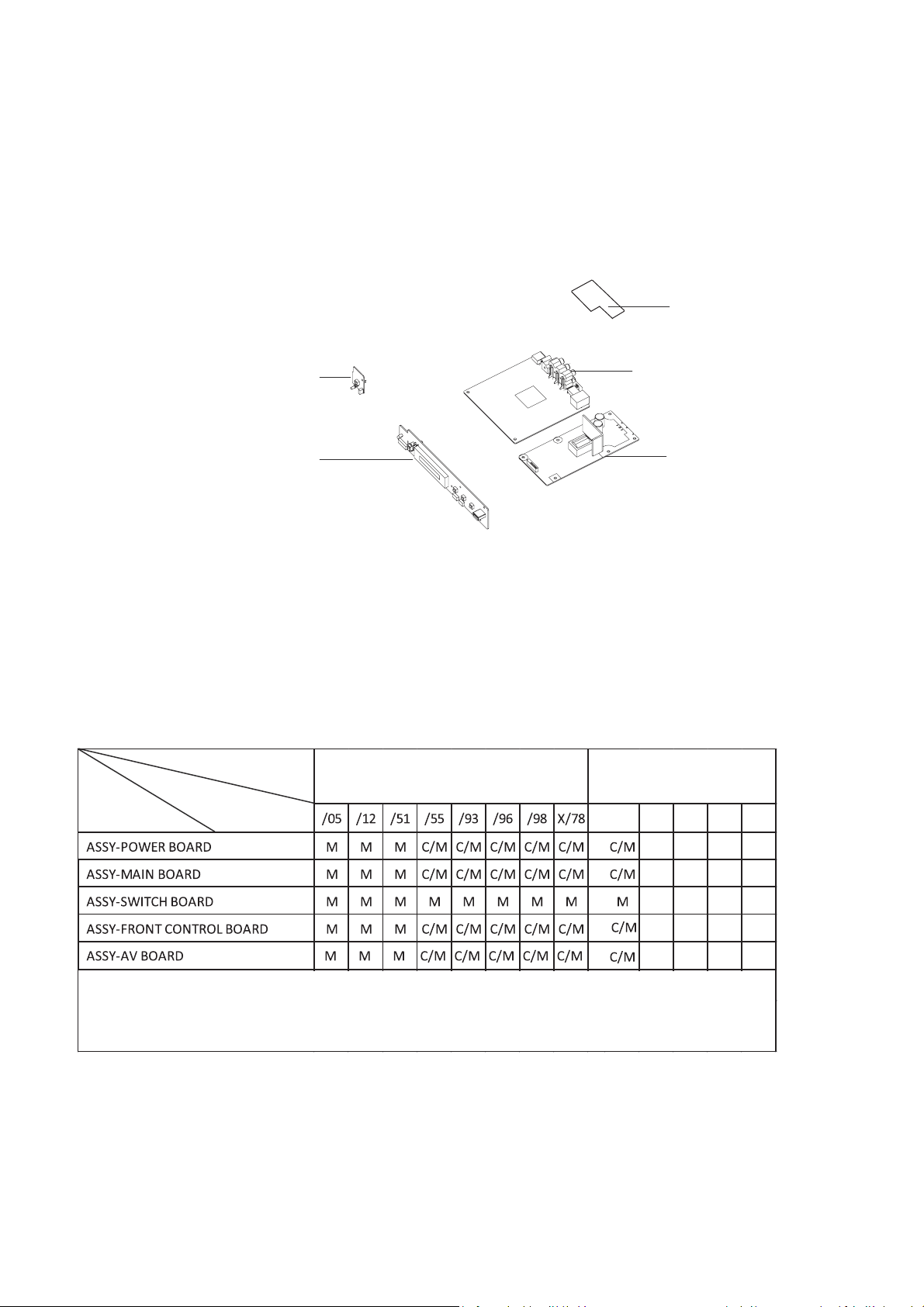
PCBS LOCATION
1-7
AV BOARD
SWITCH BOARD
FRONT CONTROL BOARD
VERSION VARIATIONS
Type / Versions
BD P3100
MAIN BOARD
POWER BOARD
BD P3080
Board in used
Service policy
* TIPS: C -- Component Lever Repair.
M -- Module Lever Repair
X -- Used
/98
Page 8
2-1
Mechanical and Dismantling Instructions
Dismantling Instruction
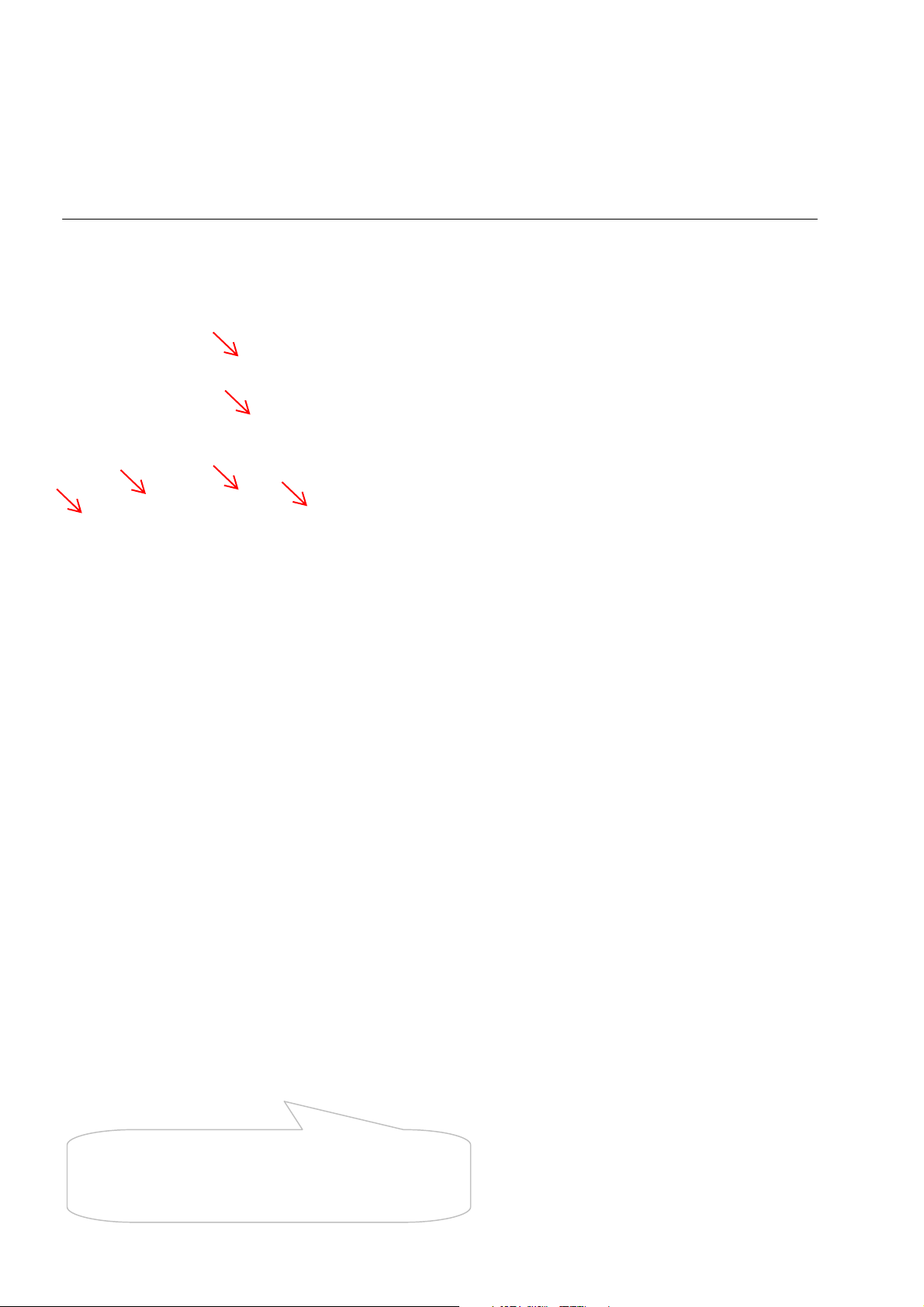
The following guidelines show how to dismantle the player.
Step1: Remove 6 screws around the Top Cover, and then remove the Top Cover (Figure 1).
Detailed information please refer to the model set.
Figure 1
Step2: If it is necessary to dismantle Loader or Front Panel, the Front door should be removed first. (Figure 2)
Note: Make sure to operate gently otherwise the guider would be damaged.
Please kindly note that dismantle the front door
assembly carefully to avoid damage tray and the front door.
Figure 2
Page 9
2-2
XP6
XP3
XP4
J3
XP2
Mechanical and Dismantling Instructions
Dismantling Instruction
Step3: If the tray can’t open in normal way, you can make it through the instruction as below (Figure 3).
Note: Make sure to operate gently otherwise the guider would be damaged.
Detailed information please refer to the model set.
Step4: Dismantling Front Panel, disconnect the connectors (
and 2 snaps of bottom cabinet , then gently pull the Panel out from the set. (Figure 4 - Figure 6)
Figure 3
J3, CN502), need release 3 snaps of Front Panel
Figure 4
Page 10

2-3
Mechanical and Dismantling Instructions
Dismantling Instruction
Step5: Dismantling Loader, disconnect the 3 connectors (XP6, XP3, XP4) aiming in the below figure, and remove 4 screws that
connects the loader and the bottom cabinet. (Figure 4-5)
Detailed information please refer to the model set.
Figure 5
Step6: Dismantling Main Board, first disconnect the connector (XP2), and then remove 6 screws. (Figure 6)
Step7: Disconnect connector (CN504, CN502) and remove 6 screws on Power Board to dismantle the Power Board. (Figure 6)
Figure 6
Page 11
3-1
Software check and upgrade
Preparation to upgrade software
1)Start the CD burning software & create a folder named "UPG_ALL",
2)Then copy the Bin file (BDP_3100_S_B.bin ) OR(BDP_5100_S_B.bin )into it,
3)Burn the data onto the blank CD or USB. 1) Power on the set and open the tray door.
4)If the model is BDP3100,must use (BDP_3100_S_X.bin )to upgrade 2) Press <Home> button on the reomote control.
If the model is BDP5100,must use (BDP_5100_S_X.bin )to upgrade
X(A;B;C)If the model BD code is A,,X=A;BD code is B,X=B;BD code is C,X=C
A. Procedure for software upgrade
A) Upgrade software via Disc
1) Power on the set and insert the prepared Upgrade <Version Info.>, then press <OK>, the software version
CDR. and other information will display on the TV screen as below:
2) The set will starts reading disc & response with the Model:BDP3XXX or BDP5XXX
following display TV screen: Versions:
Now searching for upgrade software!
Please wait…! http://www.philips.com/support
Still MAC:XX-XX-XX-XX-XX-XX
3) Press <OK> button to confirm, then screen will display :
An upgrade software has been found!
Start upgrade with version:WKXXX.X?
Cancel Start
4) Press Right cursor button to choose "Start", then press <OK>;
5) The software will updagrde and screen will display as below:
Upgrade is ongoing, Please wait…
Please do not unplug or switch off the device.
6) The screen will display as below when upgrading complete:
Upgrade has completed successfully!
Power off after 5s.
Power Off
5) Restart the set.
B. Read out the software versions to confirm upgrading
3) Select <Setup>, then press <OK>.
4) Select <Advanced Setup>, press right cursor to choose
Caution: The set must not be power off during
upgrading, otherwise the Main board will be
damaged entirely.
Remark:The region code can not be manual changed.
B) Upgrade softwar via network:
1) Setup the network connection (See "Getting started">"Set up
network").
2) In the Home menu, select <Setting>-<Advanced Setup> <Software Download>-<Network>.
* You are prompted to start upgrading processes if upgrade
media is detected.
3) Follow the instructions on the TV screen to confirm update
operation.
* Once software updated is complete, this player automatically
truns off to standby.
4) Disconnect the power cord for a few seconds and connect again
to turn on the player.
C) Update software via USB Flash Drive:
1) Go to www.philips.com/support to check if the latest software
version is available for this player.
2) Download the software onto a USB flash drive.
3) Insert the USB flash drive to the USB jack of the rear panel.
4) In the Home menu, select <Setup>-<Advanced Setup>-<Software Updade
>-<USB>.
5) Follow the instructions on the TV screen to confrim update operation.
* Once software update is complete, this player automatically turns to
standby.
6) Disconnect the power cord for a few seconds and connect again to
turn on the player.
Page 12

3 - 2
Loader repair Instruction for BDP3100/5100/ 3080/98
Preliminaries (at O.E.M. supplier site)
After scanning BARCODE on the new LOADER in supplier – TCL factory, print the
one-dimensional code which generated by scanner and computer on label, then paste it into
LOADER. If FA test passed , break off the protection point under the LOADER.
Repair Procedure in workshop
1. In region’s workshop, to install loader in the machine then weld the open protection point.
Keep the set to connect the TV and power on, press keys “5””1””7””7” on Remote Control
when in the HOME menu, then the menu will be displayed.
2. Select “Enter Barcode Info” from the menu, input the BARCODE of the LOADER and wait
until the OSD displays “PASS”, press “STOP” key on Remote Control to go back to the
menu.
3. Select “Laser check”, confirm whether the cable is connected and welded protection point is
ok.
4. Restart the set, test CD, DVD, BD discs. If ok, the LOADER replacing procedure is finish.
Page 13
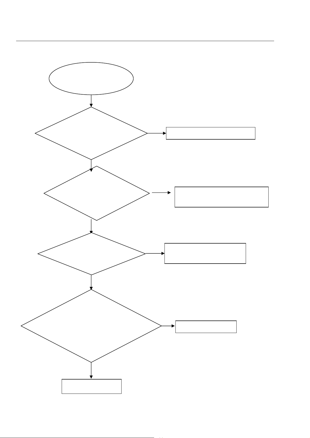
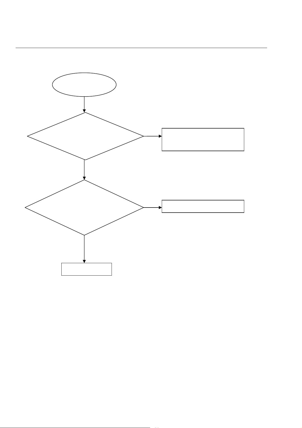
No display on VFD, and buttons do not work
No display on VFD, and
buttons do not work
Yes
Check every supply
voltage on main board is
normal
Yes
4-1
Trouble shooting chart
No
Refer to Power supply board part
Check -28V,+12V voltage on
the PSU(CN502.3,5)and
front board (JP1 3,5)
No
Fix the connection JP1 on front board
and CN502 on power board
Yes
Check the front board
signals SCLK,SDA, STB
(JP2,3,4,5)
No
Check the U4’s pin 8,9,6 arrive the
condition JP2,3,4,5
Yes
1.Check whether bad solder exists
on U3 and pins of VFD,
2.Check whether the circuit
connected to K1, K2, K3, K4, K5,
K6 is broken.
No
Correct connection
Yes
Replace U4 or VFD
Page 14
4-2
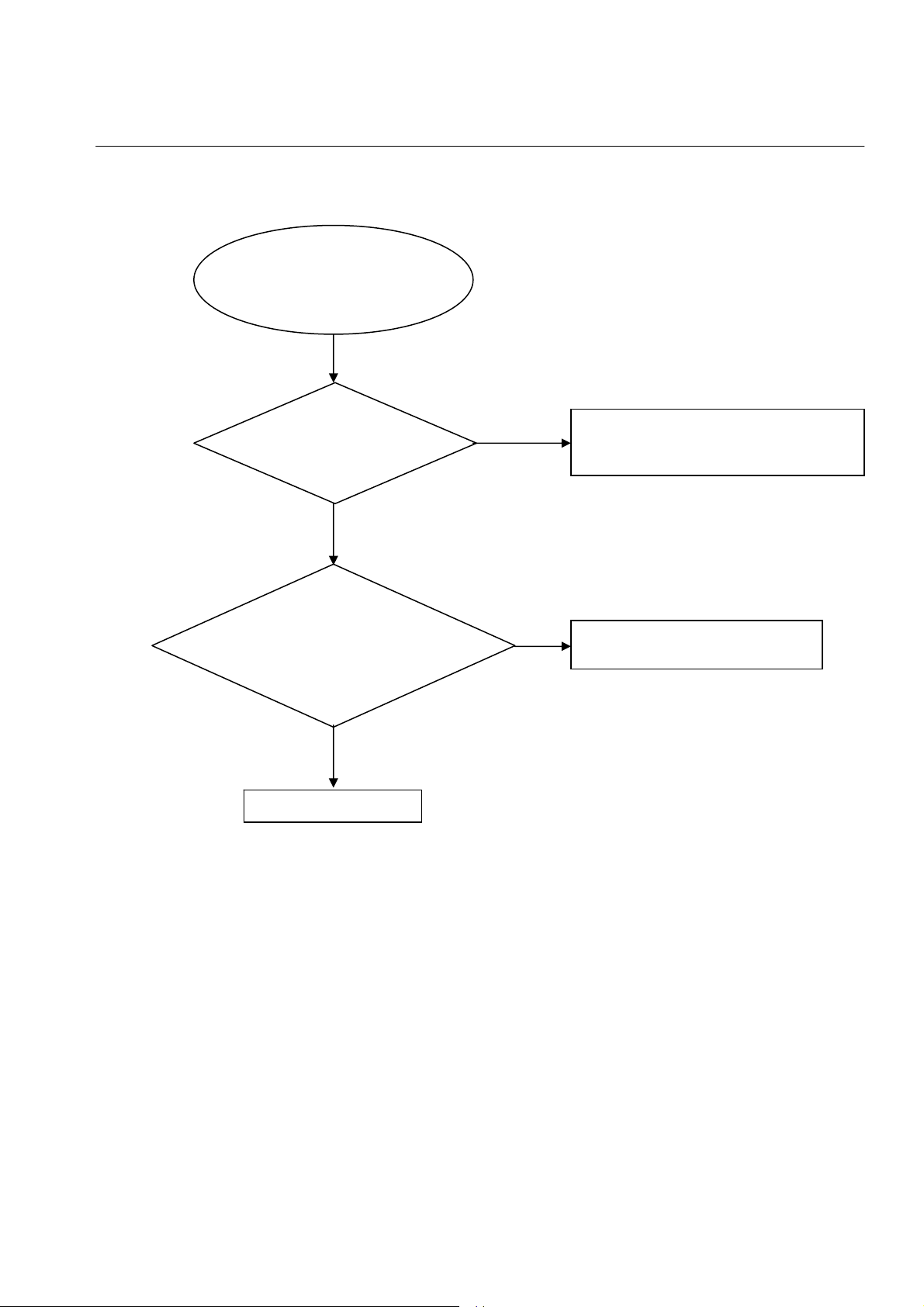
b
Trouble shooting chart
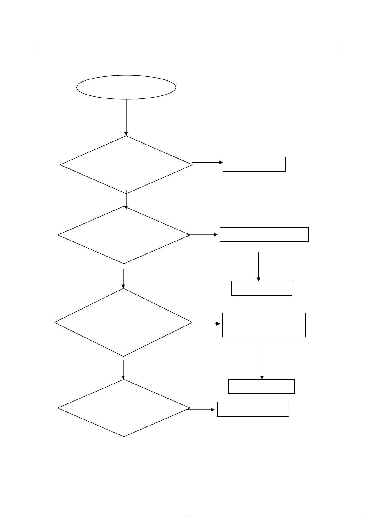
No audio output
No audio output
Go
Yes
Check if XP2 conect
ok or not from the AV
oard to mainboard
No
Fix XP2 in AV board
Check whether the audio signal
is right from the U915’9,10,11,12
No
Check the U915 power supply
Yes
Replace the U915
Check whether the audio
signal is right from the
U6’1,7
NO
Check the U6 power supply
(U6’4=-12V and U6’8=12V)
Yes
Replace the U6
Check If the C511,C501
is on
NO
Add the two set
Page 15
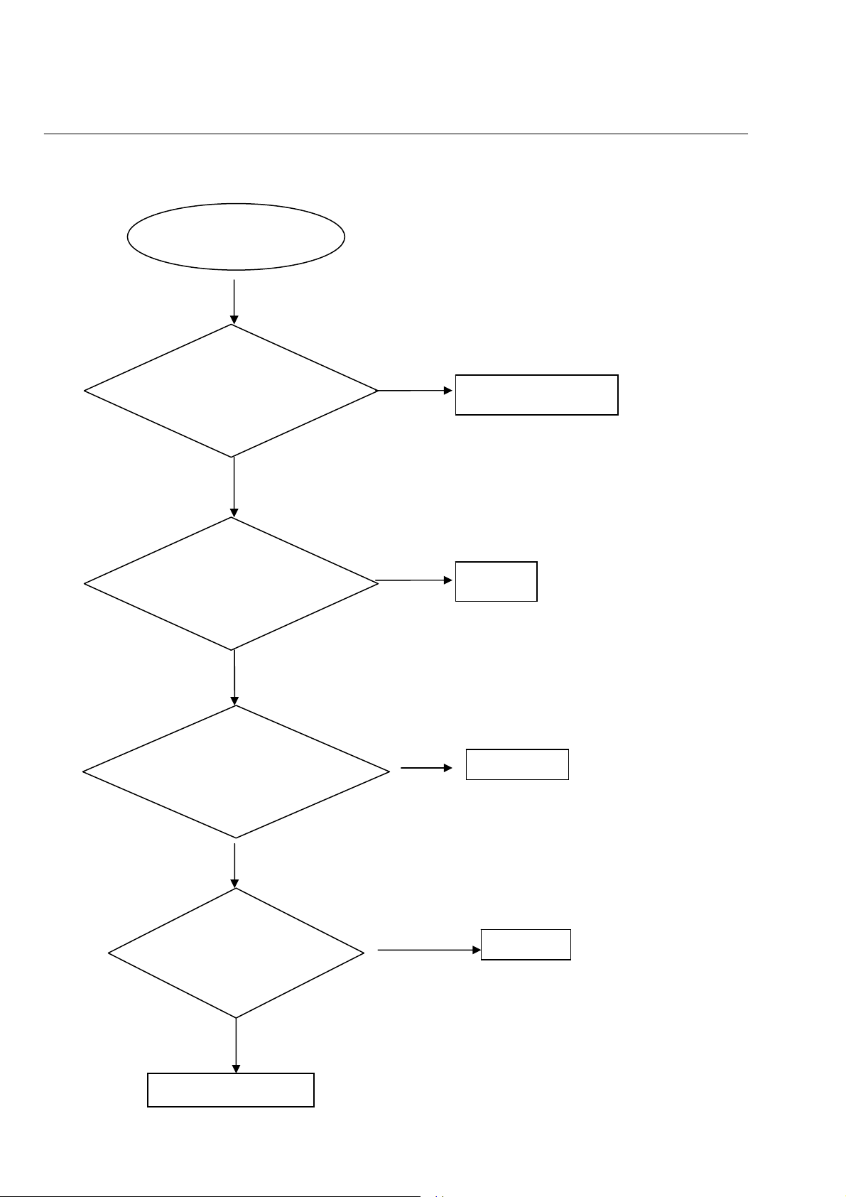
Remote control does not work
Remote control
does not work
Go
Check whether the remote
controller’s battery is
exhausted or not.
NO
Check the IR1 power
supply is OK,IR1’3 is about
5V
Yes
Replace IR1
Yes
4-3
yes
No
Trouble shooting chart
Replace the battery for remote
controller
Check the VCC net no front board
Page 16
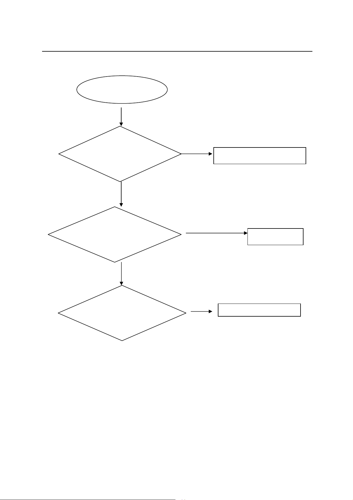
Can’t read disc or can’t open the disk door
Can’t read disc or can’t
open the disk door
GO
Check whether the
DVD loader running is
normal
Yes
Check 45pin and 8pin
cable from main board
connection to the loader is
normal
Yes
Replace the loader
4-4
Trouble shooting chart
NO
NO
Check the connection o 4pin cable from the
main board
Fix the connection the 45pin cable
Page 17
4-5
No video display
No Video display
Go
Check if XP2 fix ok or
not from AV board to
mainboard
Check R615 is on in
main board
Yes
Yes
No
Fix XP2 in AV board
No
Fix R615
Trouble shooting chart
Check if L452 is on
No
Add L452
Yes
Check If R616 is on
No
Add R616
Replace the main board
Page 18
Can not connect to network
Can not connect to
network
Go
4-6
Trouble shooting chart
Check if LFE8634 is on
In mainboard
Yes
Check
R557,R558,R559,R560,R
561 is on in main board
Yes
Check if the P400 is ok
Or not
No
Fix LFE8634 in mainboard
No
Fix all the resistor
No
Change P400
Page 19
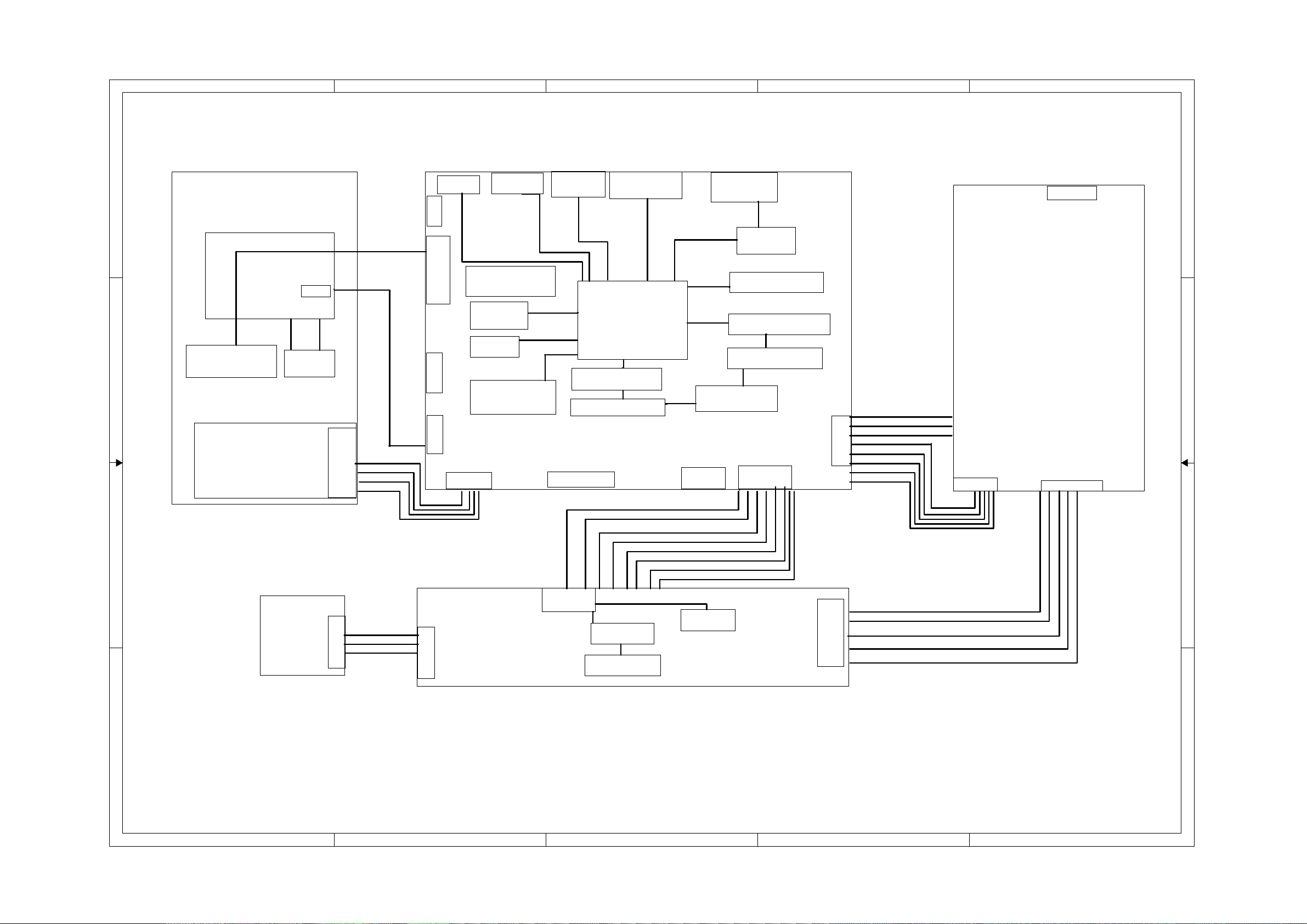
5-1 5
-1
A
B
C
D
E
BDP3100 BDP5100BDP3080/98 Wiring Diagram5
1 1
USB
7.1AV
COAX
Signal manage(45Pin)
connect board
LOADER
45PIN
OPU SANYOU 412
SA/SLED MOTOR DRIVER(8PIN)
8PIN
4PIN
4PIN
TRAVERSE
45PIN FFC (OPU)
R2A30209SP(MOTOR DRIVE)
TPC1391G4(Motor Drive)
DSP
2 2
TRAY IN/OUT BOARD
LOADLOAD+
GND
TRAYIN/OUT
TRAYIN
RS232(for FE)
8PIN(FFC)
TAY IN/OUT
RESET
3 3
COMPONENT
L.R,CVBS
MTK8530
MAIN BOARD
DDR2 1Gbit/1066
DDR2 1Gbit/1066
USB
HDMI
IR
GND
VSTB
VCLK
VD
RS232
GND
RJ45
LAN8710
NAND FLASH 2Gbit
DDR2 512Mbit/1066
DDR2 512Mbit/1066
DDR2 POWER
G2992
FB TO MB
9PIN
PCON
POWER
POWER IN
VCC_P
VCC_P
GND
GND
+12V_P
-12V
GND
+5VSTB
POWER IN
AV 220 IN
PSU
POWER FB(5pin)
FRONT BOARD
IR
POWER FB(5pin)
+5VSTB
PCON
-24V
GND
+12V
SWITCH BOARD
POWER
LED-2
GND
STANDBY+LED
FB TO MB
9IN
VFD DRIVER
S16312
VFD(vfd20-0824)
STANDBY+LED
4 4
A
B
C
D
E
Page 20
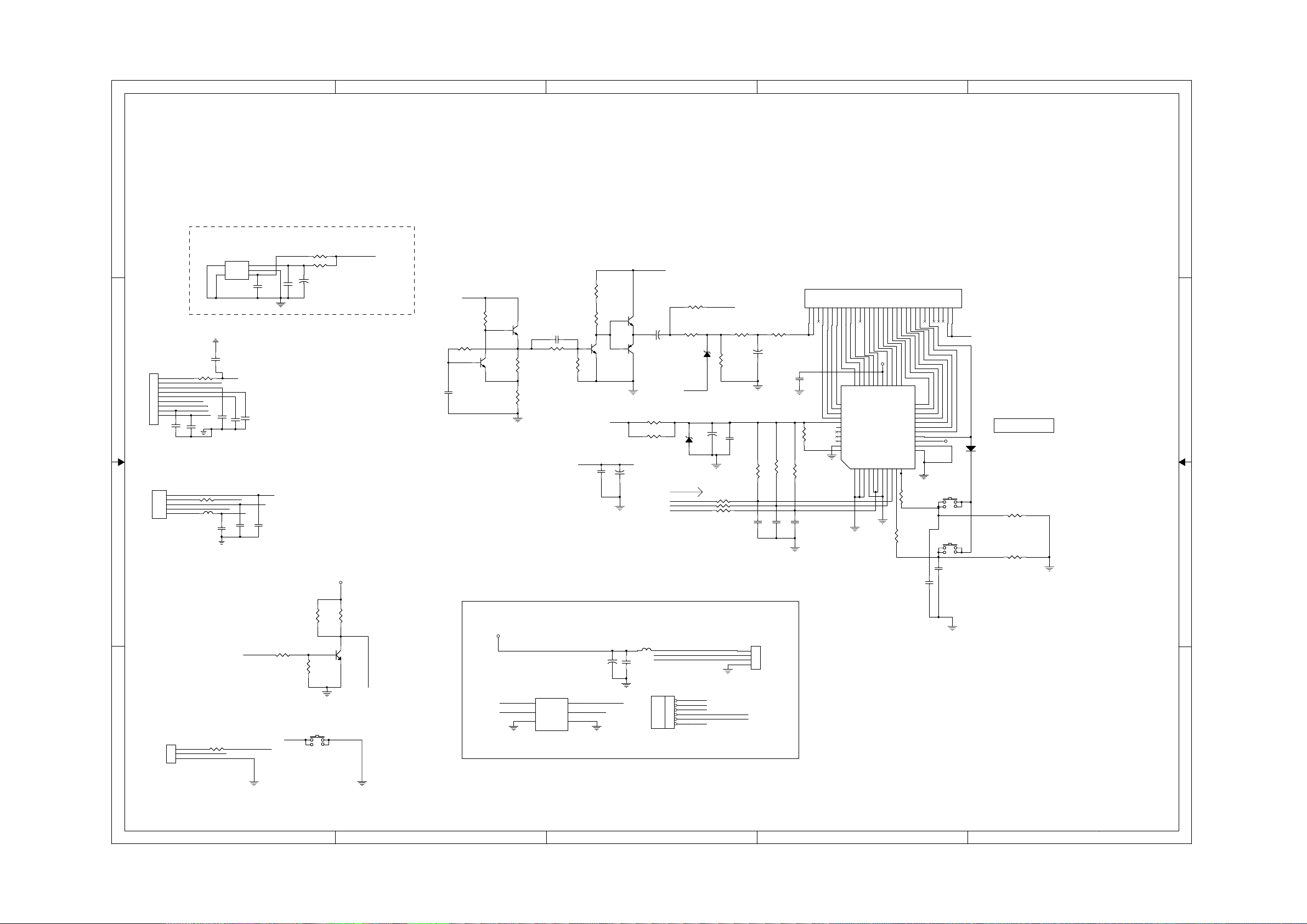
6-1 6
-1
A
B
C
D
E
Front Board Circuit Diagram:
1 1
IR CIRCUIT
IR1
IR1
3
5
VCC
GND
2
GND
1
4
IR
GND
REM
REM
R48
R48
GND
VSTB
VCLK
VD
GND
PCON
POWER
OPEN
C16
C16
100pF
100pF
GND
to power board
+5VSTANBY
R49
R49
FB1 500ȍFB1 500ȍ
100R
100R
GND
0.1uF
0.1uF
GND
C13
C13
100pF
100pF
IR
C15
C15
100pF
100pF
100
100
PCON
+12V
C25
C25
C24
C24
0.1uF
0.1uF
GND
to main board
JP2
JP2
2 2
1
2
3
4
5
6
7
8
9
9PIN/2.0mm
9PIN/2.0mm
JP1
JP1
C14
C14
100pF
100pF
5PIN/2.0mm/130mm
5PIN/2.0mm/130mm
1
1
2
2
3
3
4
4
5
5
C18
C18
100pF
100pF
C17
C17
100pF
100pF
C12
C12
47pF
47pF
-24V
C26
C26
0.1uF
0.1uF
3 3
C11
C11
0.1uF
0.1uF
+
+
CE6
CE6
47uF/16V
47uF/16V
R29
R29
R30
R30
100 ohm
100 ohm
2.2k
2.2k
+5VSTANBY
+5VSTANBYIR
+12V
VFD3
VFD3
VFD20-0824
R38
R38
10K
10K
C30
C30
100pF
100pF
AC1
R39
R39
10K
10K
C31
C31
100pF
100pF
VFD20-0824
F21F222G53G64G75G86G97G108G11NC12P1
NP31G
4
C27
C27
0.1uF
0.1uF
34
G4
35
G3
36
R23
R23
51K
51K
G2
37
G1
38
VDD
39
LED4
40
LED3
41
LED2
42
LED1
43
GND
44
OSC
P315P2
P416P517P618P719P8
13
14
20
-24V
26
31
33
27
G632G5
VEE
SEG1328SEG1429SEG1530SEG16
PT6312
PT6312
SEG6/K6
U4
U4
SEG5/K5
SEG4/K4
SEG3/K3
SEG2/K2
SEG1/K1
SW11SW22SW33SW44SDout5SDin6GND7SCLK8/CS9KEY110KEY2
SW3
SW1
SW2
R27
R27
2.2k
2.2k
P1427P1528NC29NP30F131F1
NC26P1325P1224P1123P1022P9
21
23
SEG9
SEG1024SEG1125SEG12
22
SEG8
21
SEG7
20
19
18
17
16
15
14
VDD
13
KEY4
12
KEY3
11
R28
R28
2.2k
2.2k
32
AC2
K1 K2 K3
+5V
D2
1N4148D21N4148
K2
K2
PLAY/PAUSE
PLAY/PAUSE
K3
STOPK3STOP
C22
C22
47pF
47pF
C32
C32
47pF
47pF
R32 10KR32 10K
R31 10KR31 10K
+5V
R8 18KR8 18K
C2
1000pFC21000pF
R3
10KR310K
Q5
3DG3904MQ53DG3904M
Q2
3DG3904MQ23DG3904M
R111KR11
1K
R131KR13
1K
R9 4.7KR9 4.7K
C1
0.1uFC10.1uF
R1
470R1470
R4
470R4470
Q4
3DG3904MQ43DG3904M
R12
R12
10K
10K
-24V
C5
0.1uFC50.1uF
+12V
+
+
CE3
CE3
22uF/50V
22uF/50V
Q1
3DG3904MQ13DG3904M
Q3
3CG3906MQ33CG3906M
+
+
R341KR34
1K
R351KR35
1K
CE1
CE1
3.3uF/50V
3.3uF/50V
+5V
R2 2.2R2 2.2
R5
470R5470
-24V
ZD2
ZD2
BZX79C5V1
BZX79C5V1
VSTB
VCLK
VD
AC2
R10
R10
ZD1
ZD1
10K
10K
BZX79C6V2
BZX79C6V2
+
+
CE7
CE7
47UF 16V
47UF 16V
R44 100R44 100
R43 100R43 100
R42 100R42 100
R6 330R6 330
C28
C28
0.1uF
0.1uF
R7 5.6R7 5.6
+
+
CE2
CE2
3.3uF/50V
3.3uF/50V
R37
R37
10K
10K
C29
C29
100pF
100pF
R47
R47
R33
R33
150
150
150
150
VCC
R36 10KR36 10K
+5V
JP3
PICH=2.0
PICH=2.0
JP3
R45 470R45 470
1
LED-2
2
3
POWER
4 4
OPEN
Q6
R40
R40
3904Q63904
4.7K
4.7K
OPEN/CLOSE
OPEN/CLOSE
K1
K1
LED-2
D350
D350
TVS Arrays
1
1
2
2
GND3GND
RClamp0522P
RClamp0522P
TVS Arrays
6
5
USBP1 USBP1
USBM1
CE35
CE35
220uF/16v
220uF/16v
6
USBM1
5
4
FB710
FB710
0ohm
0ohm
USBM1
C157
C157
+
+
0.1UF
0.1UF
USBP1
P600
P600
USB connector/NC
USB connector/NC
47-USB003-XX2
47-USB003-XX2
1
2
USB
USB
3
4
5
6
VCC
USBM1
USBP1
GND
pitch=2.0mm*4
pitch=2.0mm*4
1
2
3
4
GND
GND
JP4
JP4
TO SWITCH BOARD
A
B
C
D
E
Page 21
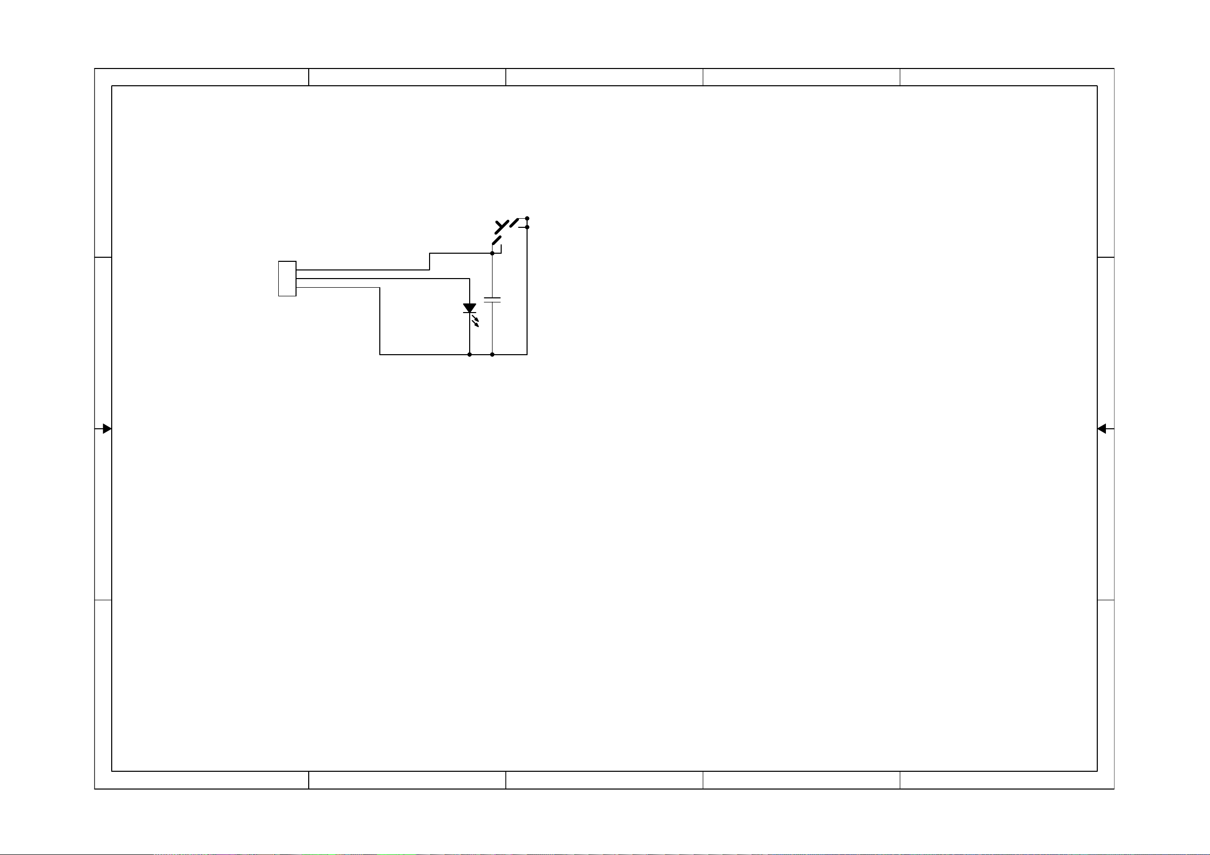
6-2 6-2
A
B
C
D
E
Switch Board Circuit Diagram:
1 1
K6
K6
POWER
POWER
PICH=2.0
PICH=2.0
1
2
3
CON1
CON1
LED2_5
LED2_5
D1
D1
C1
47PfC147Pf
2 2
SWITCH BOARD
3 3
4 4
A
B
C
D
E
Page 22
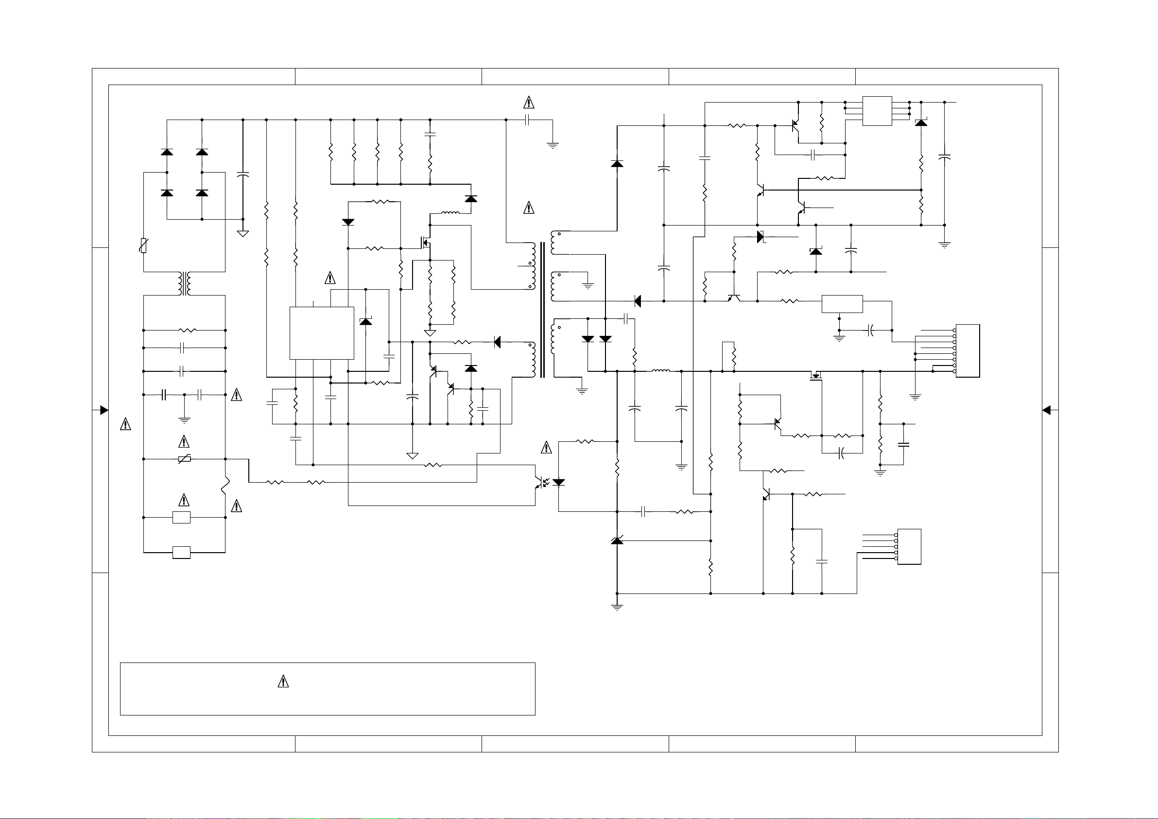
6-3 6
-3
A
Power Board Circuit Diagram:
D505
D505
RL207
RL207
1 1
D506
D506
RL207
RL207
TR501
TR501
5D205
5D205
LF501
LF501
30mH
30mH
R546 2.2MR546 2.2M
2 2
CX501
CX501
0.22uF/275Vac
0.22uF/275Vac
CX502
CX502
0.22uF/275Vac
0.22uF/275Vac
CY501
CY501
1000P/400Vac
PASPAS
1000P/400Vac
PASPAS
RV501
RV501
14K471
14K471
PASPAS
3 3
N1L
CN506
CN506
AC INPUT
AC INPUT
+1+
CN501
CN501
AC INPUT
AC INPUT
D507
D507
RL207
RL207
D508
D508
RL207
RL207
CY502
CY502
1000P/400Vac
1000P/400Vac
2
2
+
+
CE501
CE501
100uF/400V
100uF/400V
PASPAS
F501
F501
T2AL/250Vac
T2AL/250Vac
PASPAS
R508
R508
1M 1206 1%
1M 1206 1%
R507
R507
1M 1206 1%
1M 1206 1%
U501
U501
NCP1271
NCP1271
C502
C502
0.1uF
0.1uF
C504
C504
2200pF/50V
2200pF/50V
R519 1MR519 1M
R511A
R511A
150K
150K
R538
R538
33K
33K
R514 150 OHM 0805R514 150 OHM 0805
R505
R505
33K
33K
PASPAS
8
7
HV
NC
RT1COMP2CS3GND
R506
R506
18K
18K
R518 1MR518 1M
6
VCC
C503
C503
100PF
100PF
5
4
D512
D512
1N4148
1N4148
OUT
0.1U/50V
0.1U/50V
C512
C512
R511B
R511B
150K
150K
R511C
R511C
150K
150K
R516
R516
22 OHM
22 OHM
R515
R515
10k
10k
ZD501
ZD501
22V /0.5W
22V /0.5W
R5101KR510
1K
B
CE502
CE502
22UF/35V
22UF/35V
R511D
R511D
150K
150K
1
Q507
Q507
S8550
S8550
+
+
C501
C501
103/1KV
103/1KV
R51222R512
22
FB501
FB501
2.2uH
2.2uH
23
Q501
Q501
STP04NK60Z
STP04NK60Z
1R
R502B1RR502B
1R
R502A1RR502A
R513 10R513 10
Q506
Q506
S8550
S8550
R535
R535
100
100
1R
R502D1RR502D
1R
R502C1RR502C
R528
R528
2.2M 1206
2.2M 1206
D501
D501
FR107
FR107
D511
D511
1N4148
1N4148
D502
D502
FR102
FR102
C505
C505
PASPAS
CY504
CY504
102/400Vac
102/400Vac
PASPAS
5
2
3
4
1
0.47uF/63V
0.47uF/63V
T501
T501
EF25
EF25
43
PASPAS
D509
D509
SR306
SR306
12
U502
U502
PC123X
PC123X
C
9
6
7
10
6
8
R523
R523
470R
470R
C506
C506
D510
D510
SR306
SR306
3
2
D503
D503
SR3100
SR3100
222/50V
222/50V
R524
R524
2.2k
2.2k
1
U503
U503
TL431
TL431
CE505
CE505
47uF/35V
47uF/35V
D504
D504
FR107
FR107
22
R50422R504
+
+
CE509
CE509
2200uF/16V
2200uF/16V
1000uF/16V
1000uF/16V
C508
C508
0.1uF
0.1uF
L6
6.8uHL66.8uH
CE510
CE510
+M
+
+
+
+
CE503
CE503
1000uF/16V
1000uF/16V
+
+
R525
R525
1.2k
1.2k
R544 10KR544 10K
C511
C511
0.1uF/50V
0.1uF/50V
R501
R501
2.2K
2.2K
R520
R520
2.2k
2.2k
R521
R521
10k
10k
R526
R526
2.49k 1%
2.49k 1%
R527
R527
2.4k 1%
2.4k 1%
Q502
Q502
S8050
S8050
R543
R543
2.2K
2.2K
J14
J14
+M
R530
R530
10k
10k
R531
R531
2.2k
2.2k
Q504
Q504
2N3904
2N3904
D
ZD502
ZD502
30V 1/2W
30V 1/2W
0 OHM
0 OHM
+5VSTB
Q503
Q503
2N3906
2N3906
J2 0 ohmJ2 0 ohm
Q510
Q510
2N3906
2N3906
Q509
Q509
2N3904
2N3904
+12V
R522
R522
390
390
R509
R509
22R
22R
R545
R545
10K
10K
C510 0.1uF/50VC510 0.1uF/50V
JMP
R542 2.2KR542 2.2K
Q508
Q508
2N3904
2N3904
24V 1/2W
24V 1/2W
2
AOD472
AOD472
Q505
Q505
4 3
1
R541
R541
10k
10k
JMP
R533
R533
22k
22k
R534
R534
10k
10k
12-S
ZD503
ZD503
U505
U505
LM79L12
LM79L12
IN
CE513
CE513
22uF/35V
22uF/35V
PCON
C507
C507
0.1uF
0.1uF
GND
1
R532
R532
10k
10k
+
+
VO
+5V
1
2
3
Q511
Q511
PMK50XP
PMK50XP
+
+
CE507
CE507
22uF/35V
22uF/35V
CE508
CE508
22uF/35V
22uF/35V
S1
S3
S2
G14D4
-24V
3
+
+
+5VSTB
PCON
-24V
+12V
D1
D2
D3
R536
R536
22k
22k
R537
R537
10k
10k
1
2
3
4
5
8
7
6
5
12-S
CN502
CN502
4 x2.0mm
4 x2.0mm
+5VSTB
PC_ON
-24V
GND
+12V
R540
R540
100
100
R539
R539
220
220
C509
C509
0.1uF
0.1uF
ZD504
ZD504
11V /0.5W
11V /0.5W
+5VSTB
+12V
E
+12V
+
+
CE511
CE511
220uF/16V
220uF/16V
8
+5VSTB
7
GND
6
-12V
5
+12V
4
GND
3
GND
2
+5V
1
+5V
CN504
CN504
8x2.5mm
8x2.5mm
4 4
* CAUTION :
THE PARTS MARKED WITH ARE IMPORTANT PARTS ON THE SAFETY.
PLEASE USE THE PARTS HAVING THE DESIGNATED PARTS NUMBER WITHOUT FAIL.
A
PASPAS
B
C
D
E
Page 23
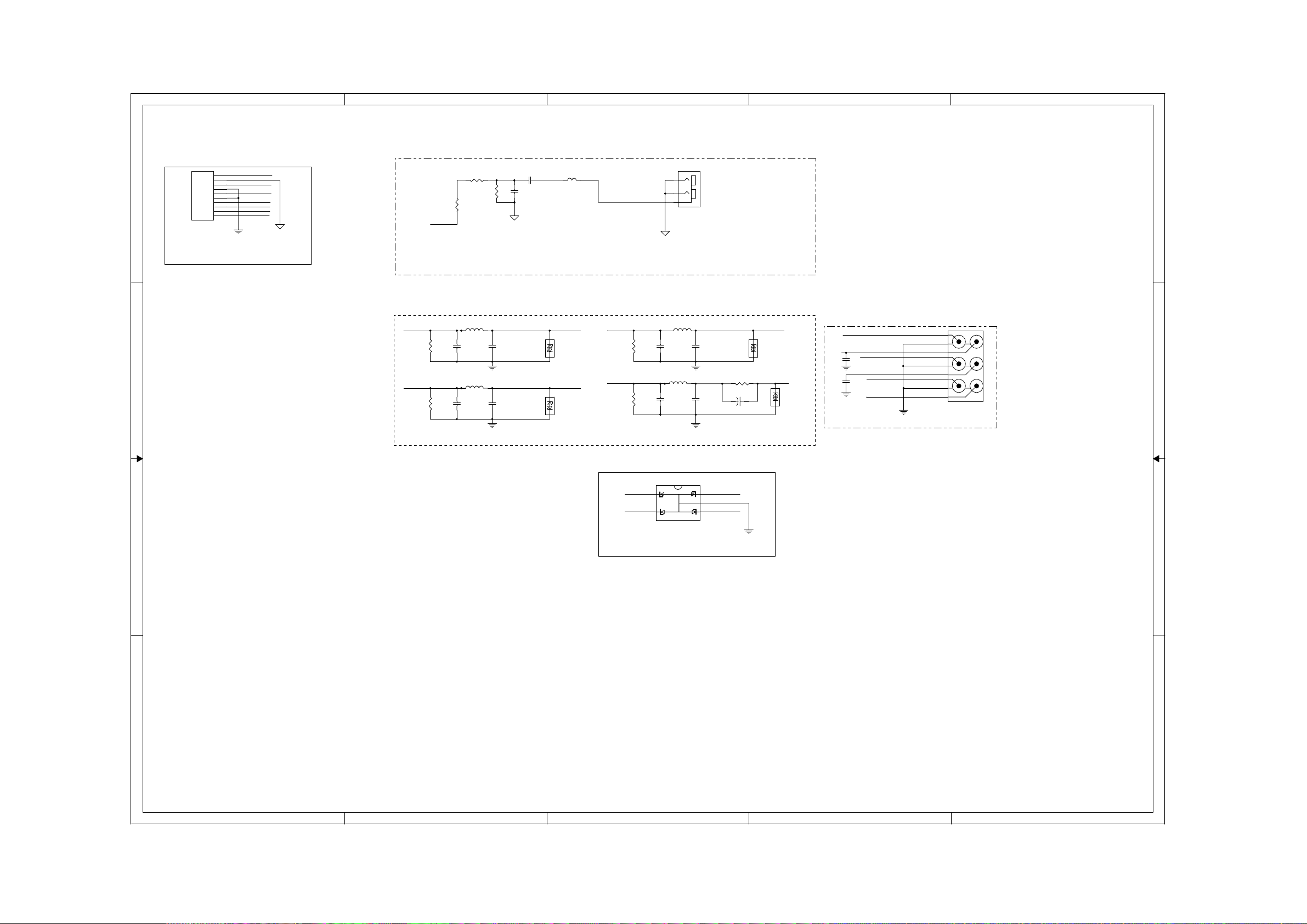
A
AV Board Circuit Diagram:
6-4
6-4
B
C
D
E
1
1
2
2
3
3
4
4
5
5
6
10
XP2
10PIN/2.0mm
6
7
7
8
8
9
9
10
1 1
ASPDIF
LOUT1
ROUT1
CVBSO
Y
Pb
Pr
FE_GND
ASPDIF
R609
R608
0
180/1%
R610
100/1%
FE_GND
C615
330pF/50V/X7R
C613
0.1uF/25V
FB1
500R
P1
1
2
3
RCA-1
FE_GND
SPDIF
SPDIF OUTOUT
VIDEO
BUFFER
Y R/V
2 2
Pb
LOW
IMPEDANCE
L456 0.22uH/0.25A
R612
75/1%
L457 0.22uH/0.25A
R613
75/1%
C617
22pF/50V/NP0
C619
22pF/50V/NP0
C616
22pF/50V/NP0
C622
22pF/50V/NP0
G/Y
D605
ESD5V0=0.016/BAV99=0.06RMB
2 1
ESDProtection>30K/35Pf
B/U
D606
2 1
ESDProtection>30K/35Pf
Pr
L458 0.22uH/0.25A
R614
C618
75/1%
22pF/50V/NP0
L452 1.8uH /0.05A
R615
C621
75/1%
47pF/50V/NP0
C623
22pF/50V/NP0
C620
47pF/50V/NP0
D601
2 1
ESDProtection>30K/35Pf
R616 0R
CE606
220uF/16V/NC
+
ESDProtection>30K/35Pf
R/V
Pr (Red)
ROUT1
Left (White)
B/U
LOUT1
G/Y
CVBS
PB (Blue)
Right (Red)
Y (Green)
CVBS (Yellow)
C629
100pF
CVBSCVBSO
D607
2 1
AV
C628
100pF
CONNECTOR
J601
RCA/6h
VIDEO OUTPUT
R/V
B/U
U70
5
4 3
PESD5VL4UG
CVBS
1
2
G/Y
3 3
4 4
A
B
C
D
E
Page 24
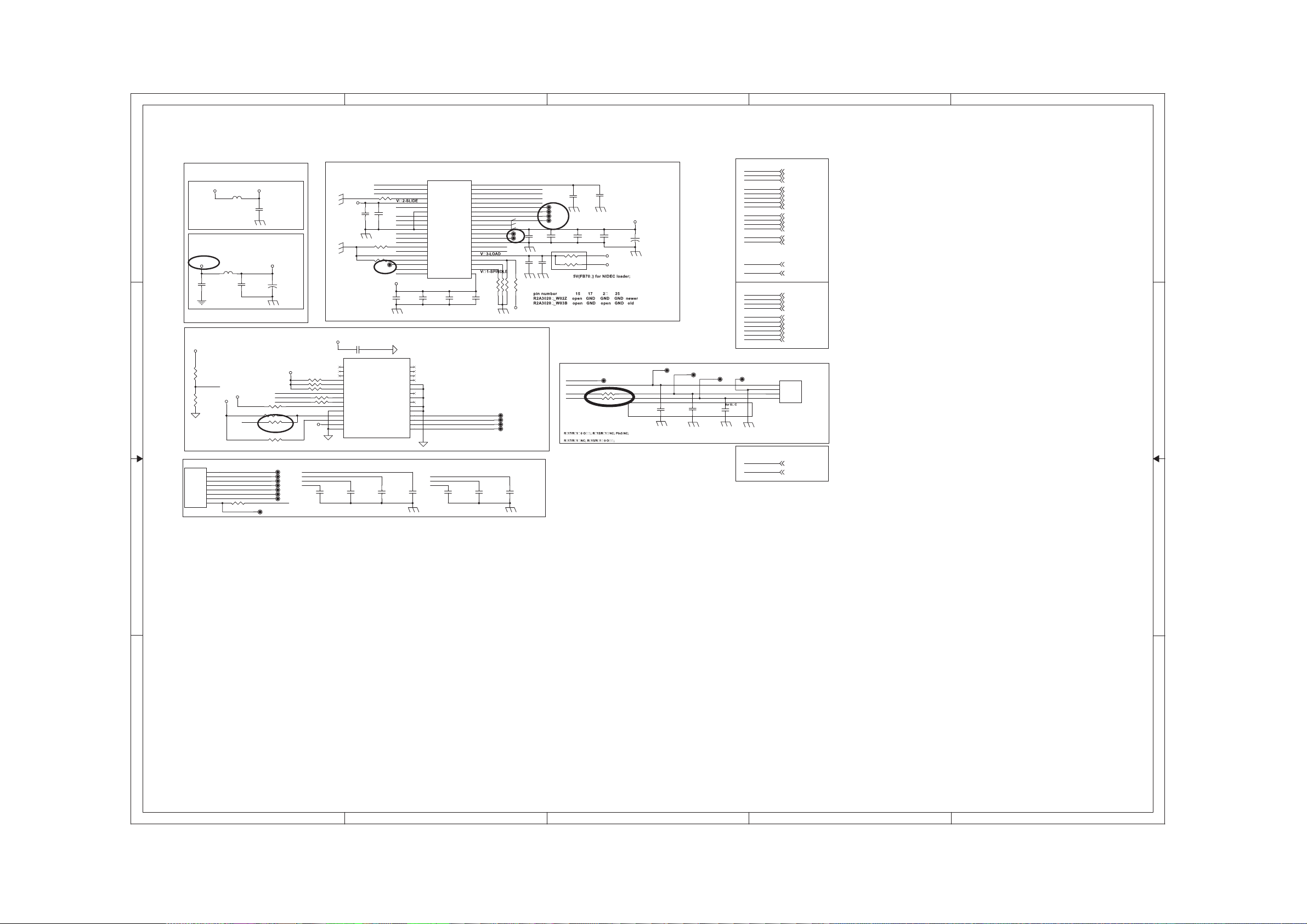
A
Main Board Circuit Diagram:POWER SOURCE
6-5
6-5
MOTOR
POWER
VCC
1
2 2
FB902
separate this 12V_P trace and other 12V_P
element(audio OP,VCC_BD_LD) from the
power source connector
12V_P
FB901 FB10/2A
C926
4.7uF/16V
A3.3V
PIN7:
GAINSW2 (GAINSW)
R772
4.7K
GAINSW2
R773
4.7K
FE_GND
8
8
7
7
6
6
5
5
4
4
3
3
2
2
1
1
HA900
8pin/1.0mm
A3.3V
R914
A+
ABB+
U
V
W
FB10/2A
C927
0.1uF/25V
MVCC
PIN12:
GIO5 (VDAC0)
GIO9
LOAD_B+
LOAD_BLOAD_A+
LOAD_A-
COMMON
0
MVCC
C928
0.1uF/25V
M
M12V
+
M
GAINSW2
FMSO4
FMSO3
R760 1K
R761 33K
R762 0/NC
R764 33K
COMMON
CE902
470uF/16V
MVCC
A+
ABB+
U
V
W
R754 1K
R757 1K
R758 1K
R765 0
R766 0
MVCC
B+
BAA+
M
4.7uF/16V/Y5V
M
Must to put these test pad
on the top side
MVCC
1
2
3
4
5
6
7
8
9
10
11
12
13
14
15
FE_GND
C902
100pF/50V/NP0
DMSO
FMSO
FMSO2
R907 8 . 2K
M12V
C913
M
R909 NC
0603-R
R910
C924
2.2uF/16V
U902
LED0
Latch_SET
Latch_CLR
SWR_SEQ1
SWR_SEQ2
SWR_OUTSEL/XMUTE
STEP_ENA
STP1_IN
STP2_IN
XLEDON
CSWON
COLLIENDZ
XRESET
A5V
AGND
TPC1391G4
C903
100pF/50V/NP0
C921
0.1uF/16V
10K
FG
M12V
Latch_RSOUT
Latch_XRSOUT
FB3P3V
REG3P3V
PGND_SW
REG1PxV
P5V_SW
FB1PxV
C904
100pF/50V/NP0
A+
A-
B+
B-
U
V
W
COMMON
FG
MUTE1
MUTE2
C912
4.7uF/16V
M
FE_GND
CSWI
CSWO
TEST1
STP2-
STP2+
STP1-
STP1+
U900
1
SPIN
2
SL1IN
3
SL2IN
4
SPLIN
5
VM2
6
SL2+
7
GND
8
SL2-
9
SL1+
10
SL1-
11
GND
12
U
13
V
14
W
15
ACTFLG
16
COMMON
17
TEST
18
SLLIM
19
FG
20
EN1
21
EN2
R2A30209SP-W02Z
SSOP42/SMD
C911
4.7uF/16V
30
29
28
27
26
FE_GND/M_GND can depend on
25
PCB layout
24
23
22
Must to put these test pad
21
on the top side
20
19
18
17
16
FE_GND
U
V
W
C905
100pF/50V/NP0
M
B
42
REF
41
LOIN
40
FOIN
39
TOIN
38
TLIN
37
TL-
36
TL+
35
FO-
34
FO+
33
GND
32
5VCC
31
TO+
30
TO-
29
GND
28
LO-
27
LO+
26
VM3
25
ACTRST
24
STTH
23
SPGS
22
VM1
C914
4.7uF/16V
0.1uF/25V
COLLIMATOR
DRIVER
CO_ACO_A+
CO_BCO_B+
C922
100pF/50V/NP0
TL- FOC1TL+ F OC1 +
FO- FOC2FO+ FOC2+
TR+
TR-
LOAD-
LOAD+
ACTRST
0
C919
R912
C923
100pF/50V/NP0
R911 0
COA+1
COA-1
COB-1
COB+1
0
R913
M
V14REF
TRAYPWM
FOSO
TRSO
TLSO
M
TR+
TR-
C918
0.1uF/25V
R908 NC
0805-R
MVCC
SLED &
SPINDER
C900
100pF/50V/NP0
M
C920
0.1uF/25V
M
M
FOC1FOC1+
Must to put these test pad
FOC2-
on the top side
FOC2+
C908
10uF/10V/NC
0805-C
R921 0
C915
R920 0/NC
4.7uF/16V
M
Trayout#
TRAYIN#
LOAD+
LOAD-
Default ASA:
Nidec:
PART
CODE:900~999
C916
C917
4.7uF/10V
0.1uF/25V
M
M
C909
C910
10uF/10V/NC
10uF/10V/NC
0805-C
0805-C
0805-R
12V(FB703) for ASA loader;
R916
R917
Trout#
M12V
MVCC
0
0
C
MOTOR
DRIVER
Sensorless
MVCC
+
CE901
220uF/16V
M
TRY
C901
100pF/50V/NP0
M
L+
C929
100pF/50V/NP0
M
L-
C930
100pF/50V/NP0
M
MOTOR DRIVER
GAINSW2
MUTE2
MUTE1
TRAYPWM
DMSO
FOSO
TRSO
TLSO
FMSO
FMSO2
FMSO3
FMSO4
TRAYIN#
TRAYOUT#
FG
V14REF
OPU
CO_BCO_B+
CO_A+
CO_A-
TR+
TRFOC1FOC1+
FOC2FOC2+
GD3
TRAY
M
GIO9
VCC
GAINSW2 (10)
MUTE2 (10)
MUTE1 (10)
TRAYPWM (10)
FMSO2 (10)
FMSO3 (10)
FMSO4 (10)
TRAYIN# (10)
TRAYOUT# (10)
FG (10)
V14REF (10)
CO_B+ (10)
CO_A+ (10)
FOC1+ (10)
FOC2+ (10)
HA901
4
4
3
3
2
2
1
1
4PIN/2.0mm
GIO9
VCC
DMSO (10)
FOSO (10)
TRSO (10)
TLSO (10)
FMSO (10)
CO_B- (10)
CO_A- (10)
TR+ (10)
TR- (10)
FOC1- (10)
FOC2- (10)
D
E
1
3 3
4 4
A
B
C
D
E
Page 25
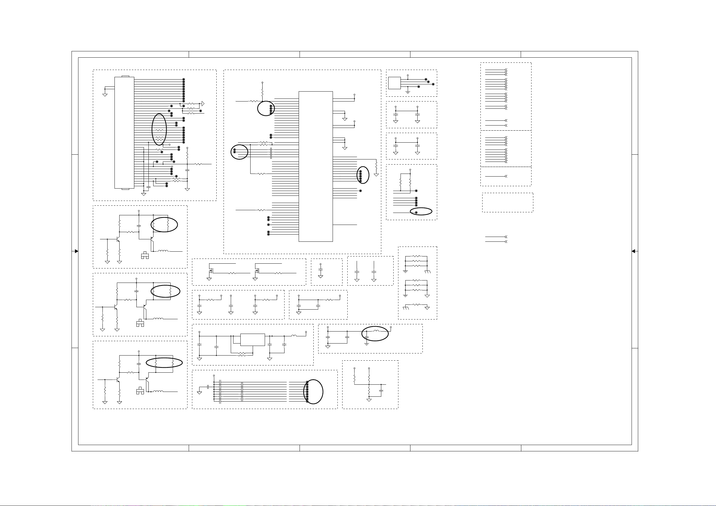
A
Main Board Circuit Diagram:MT550 DDR CHA
6-6
6-6
HA800
46
AGND
47
AGND
FE_GND
1 1
SEL_HFA_DVD
HEADER 45 SMD0.5 TOP
CON0.5-45-SMT-T-C
2 2
R823
1K
VDAC0
R818
R827
470
4.7K
FE_GND
FE_GND
3 3
VRDC2O
FE_GND
VRDC3O
R861
4.7K
R862
4.7K
FE_GND
4 4
FE_GND
FE_GND
FCS2+
FCS2-
TRK+
FCS1+
TRK-
FCS1-
VCC_CLSFT
SIG_P0
GND_CLSFT
SW3(BD)
TOP
SWB2(BD)
SWB1(BD)
VREF_PD
VCC_+5PD
GND_PD
SW(DVD/CD)
GND1
LDI_BD
LDI_CD
LDI_DVD
GND1
TEMP
VCC(HFM)
MON_CD/DVD
MON_BD
SEL_DVD
SEL_CD
SEL_HFA_CD
GND1
R825
Q806
3DG3904M
R824
1K
R826 470
Q807
3DG3904M
R828
470
R805
1K
R807 470
Q803
3DG3904M
R810
470
A-
BA+
B+
A
B
C
D
SA
SB
SC
SD
RF+
RF-
NC
470
VCC_LD
1
2N3904
VCC_BD_LD
1
2N3904
1
2
3
4
5
6
7
8
9
10
11
12
13
14
15
16
17
18
19
20
21
22
23
24
25
26
27
28
29
30
31
32
33
34
35
36
37
38
39
40
41
42
43
44
45
VCC_LD
B
B
R800 0
R858
R859 0
R860
FE_GND
C818
4.7uF/10V
2
4
2
C
1
3
B
E
2N3904
C817
4.7uF/10V
13
Q805
2
2SB1132
4
2
C
3
E
C801
4.7uF/10V
13
Q802
2
2SB1132
4
2
L800 10uH/0.015A
C
3
E
FOC2+
FOC2TRFOC1+
TR+
FOC1CO_ACO_BCO_A+
CO_B+
VCC_CLSFT
SIG_PO
INB
INA
IND
INC
ING
INH
INF
INE
RFO+
RFO-
VHAVC
BD_LD
CD_LD
DVD_LD
VCH
MDI_DVD
MDI_BD
DVD_VR
CD_VR
DVD_HFM
DVD_HFM
CD_HFM
C834
4.7uF/10V
R821
33
13
Q804
2SB1132
L801
10uH/0.015A
R819
33
L802
10uH/0.015A
R803
39
BD
LD
0
0
FE_GND1
DVD
LD
SIGP0
INB
INA
IND
LDD_SDIO
LDD_CLK
LDD_SEN
VCC_PDIC
GAINSW1
BDL
CDL
DVDL
VCC_HFM
MDD
MBD
DVR
R808 NC
R809 NC
DFM
CFM
CD
LD
R822
33
use 0603
size
CD_LD
use 0603
size
DVD_LD
use 0603
size
BD_LD
R820
33
AUX
OPU
FOC3+
FOC3-
(SanYo412)
TR1FOC4+
TR3+
FOC4CO_ACO_BCO_A+
CO_B+
R838 NC
CLSF
R856 NC
INC
ING
INH
RFO+/-,INA/B/C/D signal
INF
trace should < 6cm
INE
LDD_SD
RF1
RF2
LD1
LD2
VHA
VCP
A3.3V
GAIN
R802
10K
R852
C802
0.1uF/25V
CDR
FE_GND
Ð?
FE_GND
VCC_BD_LD
FE_GND
R804
39
FE_GND
FE_GND
0
R837
FE_GND
LED2
0
ǂ售⺜俀㕈ᚚ
VCC_PDIC AVCC
R850 0
C831
4.7uF/10V
Must to put these test pad
AUX1
on the top side
CD_VR
Q800
R801 1K
1
2 3
2SK3018
AVCC:below 0.2A AVCC:be low 0.2A
FE_GND
(change to +9V)
C832
C842
2.2uF/10V
10uF/10V
V14REF
C804 1 000pF/6.3V/NC
C807 2 200pF/6.3V/NC
C806
C809 2 200pF/6.3V/NC
0.1uF/25V
C811 33 0pF/6.3V/NC
C815 NC
CD_VR
Must to put these test pad
on the top side
DVD_VR
MDI_DVD
RFO-
RFO-
RFO+
RFO+
RFO+
RFO-
FAST_EJECT
GAINSW1
VHAVC
C820
2.2uF/10V
2
OUT
4
OUT1
R853 120/1%
R855 750/1%
C805 1 000pF/6.3V/NC
C808 0.1uF/6.3V/NC
C810 33 0pF/6.3V/NC
C812 33 0pF/6.3V/NC
B
R847
NC/47K
0603-R
R857
0
R854 0
R851 NC
R840
R841 1K
2 3
FE_GNDFE_GND
VCC_HFM AVCC
R848 0
C819
2.2uF/10V
FE_GND
OPU
POWER
ADJ
1
U802
AS1117
A3.3V
VFVREF
TRINA
TRINB
TRINC
TRIND
FOIP
FOIN
C823 0.01uF/25V
C825 0.01uF/25V
C826
0.01uF/25V
C827 0.01uF/25V
LDD_SDIO
LDD_CLK
LDD_SEN
GAINSW1
GAINSW2
GAINSW3
0
FMO3
FMO4
TLO
TRO
FOO
TYPWM
FMO1
FMO2
DMO
MUTE1
MUTE2
LED1
GIO5
GIO6
GIO6
GIO7
GIO7
JP1
GIO9
GIO9
URXD
UTXD
FESCLK
FESCLK
FESDATA
FESDAT
DVD_VR
Q801
R806 1K
1
2SK3018
3
IN
C843
1uF/25V
FE_GND
DRIVER
SIGNAL
FMSO3 FMO3
FMSO FMO1
FMSO2 FMO2
TRSO TRO
TRAYPWM TYPWM
U100F
V14REF
K6
V14
G6
FVREF
H6
HAVC
F4
TRINA
G3
TRINB
G4
TRINC
G5
TRIND
E1
INA
E2
INB
F1
INC
F2
IND
H3
INE
H4
INF
G2
ING
G1
INH
A2
FOIP
B3
FOIN
D2
FPDODVD
C1
FPDOCD
J3
RFIN
J4
RFIP
J1
RFIP2
J2
RFIN2
P2
FECFREQ
P1
FEOSCEN
R3
FECMOD
N2
FEGAINSW1
N3
FEGAINSW2
P3
FEGAINSW3
M4
FEFMO3
N1
FEFMO4
L4
TLO
K1
TRO
K2
FOO
M3
FETRAYPWM
L3
FEFMO1
M2
FEFMO2
M1
FEDMO
T1
FEGIO0
P4
FEGIO1
T2
FEGIO2
P6
FEGIO3
U1
FEGIO4
R4
FEGIO5
P5
FEGIO6
U2
FEGIO7
T3
FEGIO8
U3
FEGIO9
T6
FEGIO10
T5
FEGIO11
R5
FEGIO12
V4
FEGIO13
MT8550-DDR3-BGA492-090924
MT8550/BGA492/P0.8/B0.4/21X21
GIO5
CD/DVD
VR
VCC_LD
C835
10uF/10V
FE_GND
12V_P
FB10/2A
FB804
C844
4.7uF/16V/Y5V
FMSO4
FMSO3
FMSO
DMSO
FMSO2
TRSO
FOSO
TLSO
TRAYPWM
Must to put these test pad on the top
side
JP2
VHAVC
TRINA
TRINB
TRINC
TRIND
INA
INB
INC
IND
INE
INF
ING
INH
FOIP
FOIN
MDI_BD
LED2
FMO4FMSO4
DMODMSO
FOOFOSO
TLOTLSO
FMSO4
FMSO3
FMSO
DMSO
DMSO2
TRSO
FOSO
TLSO
PWM
AVDD12_1
AVDD12_2
AGND12_1
AGND12_2
AVDD33_1
AVDD33_3
AGND33_1
AGND33_3
AGND33_2
EQBIAS
VWDC3O
VWDC2O
VWDC1O
VRDCO
FEMPXOUT1
FEMPXOUT2
FEMPXOUT3
FEPLAY_
FELIMIT_
FEEJECT_
FETRAYOUT_
FETRAYIN_
V14REF
FE_GND
R849 0
C830
4.7uF/16V/Y5V
FE_GND
FEFG
AUX1
VDAC0
RSTI
C845
2.2uF/10V
AVCC
E5
K3
F5
L6
H5
K4
J6
L5
J5
V3
K5
D3
D1
B1
A1
E3
C2
M6
M5
N4
U6
U4
T4
W2
W1
B2
C837
10uF/10V
AVCC
FE_GND
FE_GND
FG
EQBIAS
AUX1
VDAC0
VRDC3O
VRDC2O
VRDC1O
VRDCO
MPX1
MPX2
MPX3
PLAY#
LIMIT#
EJECT#
TRAYOUT#
TRAYIN#
RSTI
C
A1.2V
A3.3V
R829
24K/1%
VRDC1
VRDCO
MPX1
MPX2
MPX3
Must to put these test pad
on the top side
LIMIT
MDI_DVD
C821
680pF/6.3V/NC
FE_GND
FE_GND
FB803 FB120/0.2A
C838
10uF/10V
A3.3V
R835
1.2K
10uF/10V
AVCC
FE_GND
FE
RS232
FE_GND
MDI_BD
C822
680pF/6.3V/NC
C836
AVCC is important for readability,
put FB803 nearby power source connector,
and AVCC trace should avoid the motor
driver signal area;
R836
2K/NC
RSTI
R839
C828
1K
0.1uF/25V
Ð ?0K/20K?
ǂ勌⅐㼬
CON801
4PIN/2.0mm
A3.3V
FE_GND
A1.2V
FE_GND
JP2
JP1
PLAY#
EJECT#
UTXD
URXD
LED1
VCC
3.3V
1
1
URXD
2
2
UTXD
3
3
4
4
C839
10uF/6.3V/X5R
C0805/SMD
C829
4.7uF/10V/X5R
0603-C
3.3V
R831
10K
FE GND
CONNECT
M
R938 0/NC
R939 0/NC
R940 0/NC
R941 0/NC
R942 0/NC
R943 0/NC
R944 0/NC
A3.3V
FE_GND
A1.2V
FE_GND
R830
10K
Must to put these test pad
on the top side
33V
URX
UTX
GD
3.3V/A3.3V,GND/FE_GND
can depend on PCB layout
C840
0.01uF/6.3V/X5R
C841
0.01uF/16V/X5R
JP2
PLAY
EJECT
UTXD
URXD
FLED1
M
FE_GND
FE_GND
PART
CODE:800~899
D
MOTOR DRIVER
GAINSW2
MUTE2
MUTE1
TRAYPWM
DMSO
FOSO
TRSO
TLSO
FMSO
FMSO2
FMSO3
FMSO4
TRAYIN#
TRAYOUT#
FG
V14REF
OPU
CO_BCO_B+
CO_A+
CO_A-
TR+
TR-
FOC1-
FOC1+
FOC2-
FOC2+
CNT
FAST_EJECT
1. LED IO
䴰㾱⺞䇔⍻䈅᧗ࡦ DŽ
2. PCB DDR
䴰㾱 䵢䬌˗
3. TP1391
䴰㾱⺞䇔 ެᇩᙗ˗
4.
䴰㾱
GIO9
VCC
GAINSW 2 (11)
MUTE2 (11)
MUTE1 (11)
TRAYPW M (11)
DMSO (11)
FOSO (11)
TRSO (11)
TLSO (11)
FMSO (11)
FMSO2 (11)
FMSO3 (11)
FMSO4 (11)
TRAY IN# (11)
TRAYOUT # (11)
FG (11)
V14REF (11)
CO_B- (11)
CO_B+ (11)
CO_A+ (11)
CO_A- (11)
TR+ (11)
TR- (11)
FOC1- (11)
FOC1+ (11)
FOC2- (11)
FOC2+ (11)
FAST_EJECT
GIO9
VCC
E
(7)
A
B
C
D
E
Page 26
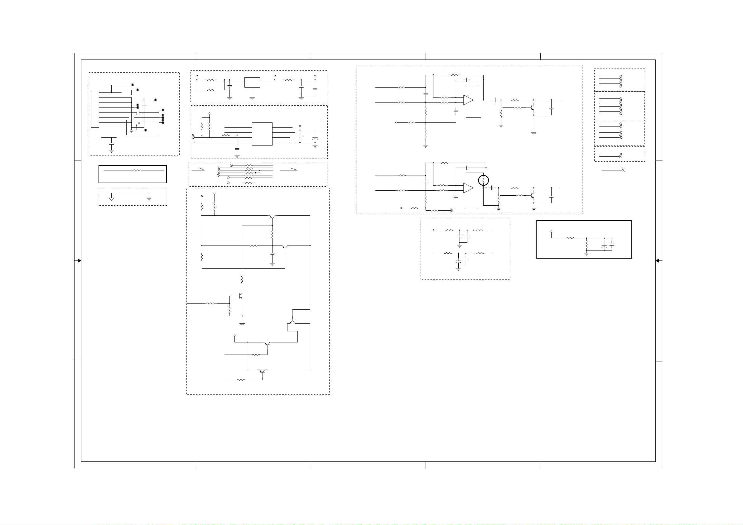
A
Main Board Circuit Diagram:MT550 DDR CHB
6-7
6-7
B
C
D
E
12V_P REFA
R189
4.7K
MT8550
VCC
R139
3.3K
R138 100
R176 100
AVSCK
AVSDA
AOBCK_R
AOSDATA0_R
AOSDATA4_R
AOLRCK_R
3.3V
R183
4.7K
R191 330
AOMCLK_R
SCL
SDA
12V_P
R947
R946
0R/NC
0
5V_STBY/12V
()
ᔰᵪ䶉丣
()
ޣᵪ䶉丣
HA700
SCL
1
SDA
2
3
AOMCLK
4
5
AOLRCK
6
AOBCK
7
AOSDATA0
8
AOSDATA1
CON14
9
10
11
12
13
14
AOMCLK
MUTE
AOSDATA2
AOSDATA3
CON_MUTE
C719
100pF/6.3V/NC
GND
1 1
SCL
SDA
AOLRCK
VCC
R732 0/NC
C69
0.1uF
VC
CON_MUTE
AOMCLK
AOBCK
AOSDATA0
AOSDATA1
AOSDATA2
AOSDATA3
MUTE
DAC_RST#
DAC_CS#
2 2
0.1uF/25V
AAMCLK
AABCK
AASDATA
AALRCK
C130
78L05
C109
0.01uF
R214 33
R215
R216
R956
R217
R90 1K
R91 1K
U7
3
IN
1
2
3
4
5
6
8
R133 10K
R147
4.7K
OUT
GND
2
MCLK
BICK
SDTI1
LRCK
PDN
CSN
CCLK7AOUTR+
CDTI
U8
4385DA
33
DA_VDD
R76 220
1
CLOSED TO AKM4385
DAC Power Supply
16
DZFL
15
DZFR
14
VDD
13
VSS
FL+
12
AOUTL+
AOUTL-
AOUTR-
AAMCLK
33
AABCK
AASDATA
33
NC
AALRCK
AVSCK
AVSDA
11
10
9
Q13
3CG3906M
R100
4.7K
+
CE27
470uF/16V
DAC
FLFR+
FR-
MUTEL
MUTER
Q14
3CG3906M
DA_VDD
C939
10uF
C150
0.1uF/25V
DAC
C152
0.1uF/25V
+
C938
47uF/16V
FL-
FL+
FR-
FR+
R179 5.6K/1%
R153 5.6K/1%
REFA
R162 5.6K/1%
R160 5.6K/1%
REFA
R103
R175 5.6K/1%
C123
R172 470/1%
3300pF
R169 470/1%
R174
5.6K/1%
0R/NC
R102
0R
R166 5.6K/1%
C124
3300pF
R159 470/1%
R161 470/1%
R178
5.6K/1%
0R/NC
R99
R101
N12V
0R
R97
C942
4.7uF/16V/Y5V
R98 100
C119
680pF/50V/NP0
C122
680pF/50V/NP0
100
+
-
6
+
5
8 4
-
2
+
3
8 4
CE17
100uF/16V
C121
680pF/50V/NP0
-12VA
U903B
7
NJM4558 OPA
SOP8-244-1.27
+12VA
C120
680pF/50V/NP0
-12VA
U903A
1
NJM4558 OPA
SOP8-244-1.27
+12VA
R59 100
C67
0.1uF/25V
R62 100
C68
0.1uF/25V
+12VA12V_P
R104
0R/NC
-12VA
10uF
C941
C940
10uF
R180
10K
R181
MUTE_L
R167 470
R164
10K
R173 470
MUTE_R
R152 470
470
LOUT1
Q48
3DG3904M
ROUT1
Q50
3DG3904M
C126
100pF/50V/X7R
C127
100pF/50V/X7R
OP
+12VA
only for BDP2600
R86 33K
Power for OP/Close to OP
AUDIO CNT
AMUTE
AMUTE (5,7)
DAC_RST#
DAC_RST# (6)
DAC_CS#
DAC_C S# (6)
SCL
SCL (6)
SDA
SDA (6)
AUDIO I2S for Audio Board
AOMCLK
AOMCLK (5)
AOLRCK
AOLRCK (5)
AOBCK
AOBCK (5)
AOSDATA0
AOSDATA0 (5)
AOSDATA1
AOSDATA1 (5)
AOSDATA2
AOSDATA2 (5)
AOSDATA3
AOSDATA3 (5)
AOSDATA0_R
AOSDATA0_R (5)
AOSDATA4_R
AOSDATA4_R (5)
AOMCLK_R
AOMCLK_R (5)
AOBCK_R
AOBCK_R (5)
AOLRCK_R
LOUT1
ROUT1
+
VCC
C47
0.1uF
AOLRCK_R (5)
LOUT1 (8)
ROUT1 (8)
VCC
AUDIO I2S for Main Board
AUDIO OUT
REFA
R87
CE19
10K
100uF/16V
Q15
MUTER
R171
22K
DA_VDD
R177
1K(NC)
3DG3904M
Q51 9012(NC)
R157
1K(NC)
Q49 9012(NC)
Q19
BAT54A
MUTE_L
MUTE_R
MUTE
3
1 2
mute circuit
AMUTE
R945 4.7K
3 3
MUTEL
when using AK4385
4 4
A
B
C
D
E
Page 27
A
Main Board Circuit Diagram:MT8550 AV
6-8
6-8
B
C
D
E
1 1
GND5
VCC3
AV
Y1
Y1 (5)
Y2
Y2 (5)
Y3
Y3 (5)
Y6
Y6 (5)
LOUT1
LOUT1 (9)
ROUT1
ROUT1 (9)
ASPDIF
ASPDIF (5)
VCC
VCC
10PIN/2.0mm
ASPDIF
1
1
2
2
LOUT1
3
3
4
4
ROUT1
5
5
6
6
7
8
9
10
XP3
R948 33
7
R950 33
8
R949 33
9
R951 33
10
Y3
Y2
Y6
ASPDIF
Y6
Y2
Y3
Y1
Y1
NC/0R
R959
VCC
RC
CVBS
G/Y
B/U
R/V
R958
0R
2 2
3 3
4 4
A
B
C
D
E
Page 28
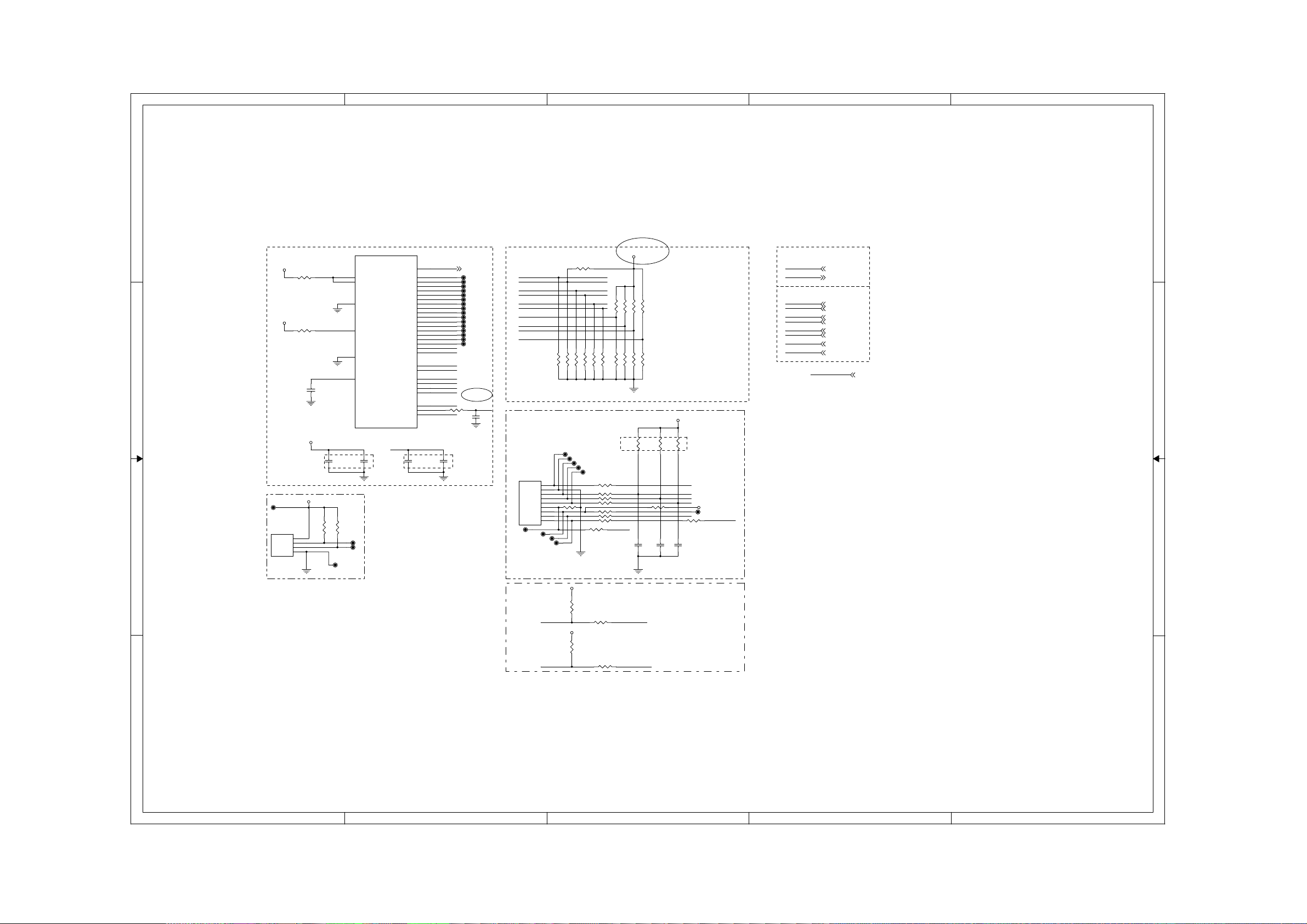
A
Main Board Circuit Diagram: MT8550 FLASH/USB/ETH/GPIO
6-9
6-9
B
C
D
E
1 1
CNT
RESET#
FAST_EJECT
HW TRAPPING
NFWEN
NFREN
NFCEN
NFCEN2
NFCLE
NFALE
SFCS
RESET# (2)
FAST_EJECT (10)
NFW EN (6)
NFREN (6)
NFCEN (6)
NFCEN2 (6)
AMUTE (5)
NFCL E (6)
NFALE (6)
SFCS (6)
OPWRSB
OPWRSB
R505 10K
100pF/50V/NP0
3.3V
HW Trapping Pin
Default value as below:
(else system will enter test mode)
--------------------------------------------------------------------* ETTXEN: 1
LCDRD: 0
NFWEN: 0
NFREN: 0
NFCEN/NFCEN2: 00
---------------------------------------------------------------------
R503 10K
R513 10K/NC
R957 10K/NC
R506 10K/NC
10K
--------------------------------------------------------------------| SFCS: reserve
| AMUTE: [ L(Default) H(Main ICE)]
R502 10K/NC
R514 10K/NC
R516 10K
| NFCLE: [ H(Default , Nand)]
R504
--------------------------------------------------------------------| NFALE: [ L(ROM/NA ND boot) H(NOR boot)]
---------------------------------------------------------------------
5V_STBY
R511 10K/NC
R508 10K/NC
R507 10K/NC
IR
VSTB
VCLK
VDATA
R954 0R/NC
OPWRSB
POWER
OPEN
5V_STBY
C6
C510
100pF/50V/NP0
100pF/50V/NP0
12V_P
PWR_CTRL#
R953 0R/NC
C508
FAST_EJECT
U100D
3.3V_STBY
3.3V_STBY
2 2
RS232
33STB
3 3
J506
4PIN/2.0mm
R509 0
R520 0
VCC3IO_STB
Close to
IC
3.3V_STBY
1
1
2
2
3
3
4
4
VCC3IO_STB
AVDD33_LDO
AVDD10_LDO
C500
NC
VCC3IO_STB
R521
10K
UARXD
UATXD
J20
DVCC33_IO_STB
J21
DVCC33_IO_STB
F22
DGND
L20
AVDD33_LDO
L19
AVSS33_LDO
K19
AVDD10_LDO
MT8550-DDR3-BGA492-090924
MT8550/BGA492/P0.8/B0.4/21X21
C501
4.7uF/10V
R523
10K
UARXD
UATXD
GND3
C502
0.01uF/25V
GPIO8
ETCOL
ETCRS
ETMDC
ETMDIO
ETRXCLK
ETRXD0
ETRXD1
ETRXD2
ETRXD3
ETRXDV
ETRXER
ETTXCLK
ETTXD0
ETTXD1
ETTXD2
ETTXD3
ETTXEN
ETTXER
UARXD
UATXD
VSTB
VDATA
VCLK
LCDRD
RESET_
OPWRSB
AVDD33_LDO
IR
GPIO8
J24
K20
F23
J25
K25
G24
F25
G20
H21
G25
F24
E25
G23
G22
G21
H20
H23
H22
E24
J22
J23
L21
L22
L23
K22
K21
K23
K24
IR Reset ESD
઼ؑ ؑⲴཚ䘁ˈ䴰㾱㘳㲁 DŽ
C503
4.7uF/10V
MOPEN
ETTXEN
POWER#
UARXD
UATXD
VSTB
VDATA
VCLK
LCDRD
IR
R923 1K/1%
OPWRSB
Close to
IC
C504
0.01uF/25V
GPIO8
TP513
TP515
TP514
TP512
TP510
TP511
TP509
TP508
TP507
TP506
TP504
TP505
TP503
TP502
TP501
TP500
Close to MT8550
RESET#
C931
0.1uF/25V
1
2
3
4
5
6
7
8
9
POW
1
2
3
4
5
6
7
8
9
OPEN
R515 10K
R952 0
R501 10K/NC
R522 10K
R500 10K
R517 10K
IR
GND4
VSTB
VCLK
R955 0R/NC
R512 10K
VDATA
R929 100
R8 100
R931 100
R933 100
R935 100
R936 100
R937 100
LCDRD
ETTXEN
NFWEN
NFREN
NFCEN
NFCEN2
SFCS
AMUTE
NFCLE AMUTE
NFALE
5VB
OP
J501
10PIN/2.0mm
POWER#
MOPEN
3.3V_STBY
3.3V_STBY
R401
4.7K
R397
4.7K
R403
2.2K
R408
2.2K
POWER
OPEN
need MTK cofirm again
4 4
A
B
C
D
E
Page 29
A
Main Board Circuit Diagram: MT8550 STBY MCU
6-10
6-10
3.3V
TP416
1 1
TP417
TP415
TP402
2 2
3 3
U100E
G12
DVCC33_IO_6
M7
DVCC33_IO
P7
DVCC33_IO
Y7
DVCC33_IO_2
E20
DVCC33_IO_3
F19
DVCC33_IO_3
N7
DVCC33_IO
SFCS
A20
SFCS
SFCK
C20
SFCK
SFDI
B20
SFDI
SFDO
D20
SFDO
NFALE
D21
NFALE
NFCEN
C22
NFCEN
NFCLE
B22
NFCLE
NFRBN
B23
NFRBN
NFREN
A23
NFREN
NFWEN
C21
NFWEN
NFCEN2
A22
NFCEN2
NFRBN2
A24
NFRBN2
NFD0
C23
NFD0
NFD1
A25
NFD1
NFD2
B24
NFD2
NFD3
B25
NFD3
NFD4
C24
NFD4
NFD5
C25
NFD5
NFD6
D24
NFD6
NFD7
D25
NFD7
GPIO0
D8
GPIO0
GPIO1
A7
GPIO1
GPIO2
B7
GPIO2
GPIO3
C7
GPIO3
GPIO4
AC4
GPIO4
GPIO5
AA5
GPIO5
GPIO6
AC3
GPIO6
GPIO7
AB4
GPIO7
SCL
D7
SCL
SDA
E8
SDA
TTDO
AC1
TDO
TTRST#
AE1
TRST_
TTDI
AD2
TDI
TTMS
AD1
TMS
TTCK
AC2
TCK
AE2
EFPWRQ
R439
0
MT8550-DDR3-BGA492-090924
MT8550/BGA492/P0.8/B0.4/21X21
GPIO7 USB_EN1#
GPIO4 DAC_RST#
GPIO3 USB_OC2#
GPIO2 USB_OC0#
GPIO1 USB_EN0#
GPIO0 USB_EN2#
IC 3.3V POWER C
C434
0.01uF/25V
C438
0.1uF/25V
F19/E20
C433
C436
0.1uF/25V
0.1uF/25V
G12M7/N7/P7
3.3V
AVDD33_USB_1P
AVDD33_USB_2P
AVSS33_USB_1P
AVSS33_USB_2P
AVDD12_USB_1P
AVDD12_USB_2P
AVSS12_USB_1P
AVSS12_USB_2P
DAC_CS#GPIO6
USB_OC1#GPIO5
MAIN POWER
C409
10uF/10V
C440
0.1uF/25V
Y7
C439
0.1uF/25V
ICE/FE232/BC
USB_DP0
USB_DM0
USB_DP1
USB_DM1
USB_DP
USB_DM
USB_VRT
USB_VRT_1P
AVDD12_COM
AVDD12_REC
AVSS12_COM
AVSS12_REC
AVDD33_COM
AVDD33_LD
AVDD33_REC
AVSS33_COM
AVSS33_LD
AVSS33_REC
TXVN_0
TXVP_0
TXVN_1
TXVP_1
TANA_0
TANA_1
GPIO
5.1K/1%
C410
1uF/16V
C411
1uF/16V
5.1K/1%
R429
4.7K
3.3V
R449 0
C402
10uF/10V
R450 0
C405
10uF/10V
C428
0.1uF/25V
0.1uF/25V
3.3V
R411
4.7K
SCL
SDA
R409 10K/NC
R410 10K
R413 10K
C426
IIC
R421 10K
3.3V
1.2V
C430
1uF
C432
1uF/16V
Default: R325=NC,R335=10K;
ICE: R325=10K,R335=NC;
R423 10K
R425 10K
R412 10K/NC
C427
0.1uF/25V
R436 0
R434 0
R438 0
R435 0
R437 0
C431
1uF/16V
HA400
TTRST#
8
DIP
7
6
TTCK
5
4
TTDO
3
2
1
H8S/P1.0
BE
ICE
GDND
1.2V
3.3V
TTDI
TTMS
33VC
VDD3.3_USB
Y3
AA3
C401
0.01uF/25V
Y4
AA4
VDD1.2_USB
V5
W4
C404
0.01uF/25V
W5
W6
USBP0
AB2
USBM0
AB1
USBP1
AA2
USBM1
AA1
USBP2
Y2
USBM2
Y1
PAD_VRT
R415
AB3
PAD_VRT2
R414
W3
AVDD12_COM
E7
AVDD12_REC
F7
C429
F9
0.1uF/25V
F8
AVDD33_COM
C6
AVDD33_LD
C5
AVDD33_REC
D4
C443
0.1uF/25V
D6
D5
E6
TXVN_0 TP_TX-
B4
TXVP_0 TP_TX+
A3
TXVN_1 TP_RX-
B5
TXVP_1 TP_RX+
A4
TANA_0
B6
A6
A5
REXT
TANA_1
REXT
TP403
TP404
R440 24K/1%
SCL
SDA
TTRST#
TTDI
TTMS
TTCK
TTDO
B
U400
R441 10K/NC
No Libary
2413
2413
1
NC
2
NC
3
NC
4
NC
5
NC
6
SE
7
R/B
8
RE
9
CE
10
NC
11
NC
3.3V
12
VCC
13
VSS
14
NC
15
NC
16
CLE
17
ALE
18
WE
19
WP
20
NC
21
NC
22
NC
23
NC
24
NC
R442 10K/NC
U9
7
IN
1
/EN1
OUT1
2
/OC1
OUT2
3
/OC2
GND
4
/EN2
G526
SO8
USB differential impedance 90 OHMUSB differential impedance 90 OHM
C936
0.1uF/25V
48
NC
47
NC
46
NC
45
NC
NFD7
44
I/O7
NFD6
43
I/O6
NFD5
42
I/O5
NFD4
41
I/O4
40
NC
39
NC
38
NC
C403
3.3V
37
VCC
0.1uF/25V
36
VSS
35
NC
34
NC
33
NC
NFD3
32
I/O3
NFD2 NFWEN
31
I/O2
NFD1
30
I/O1
NFD0
29
I/O0
28
NC
27
NC
26
NC
25
NC
NAND08GW3B2C
TSOP48-787-0.5
VCC
VCC
CB401
0.1uF/16V
USB_VCC2
USBM1
USBP1
R430 10K
R428 10K
USB_EN0#
USB_OC0#
USB_OC1#
USB_EN1#
R432
R433
10K
10K
USB differential impedance 90 OHM
MTK suggest W/S/GS=7.5/7.5/20
BACK USB
TDK ACM2012H-900-2P/0
TP_RX-
L859
TP_RX+
TDK ACM2012H-900-2P/0
TP_TX-
L860
TP_TX+
R404 4.7K
5
8
6
USBM1
USB_EN2#
USB_OC2#
R405 NC
USBP1
C937
0.1uF/25V
3.3V
R406 10K
R407 4.7K
8
6
5
4
3
1
NAND
FLASH
R416 0R /NC
NFRBN
NFREN
NFCEN
R418 0R/NC
C406
0.1uF/25V
NFCEN3
NFCEN4_R
NFCLE
NFALE
NFWP#
GND1
USBP0
USBM0
USB_VCC1
USBP0
USBM0
USB_VCC1
C372
0.1uF
USB_VCC1
USB_VCC2
CE400
CB402
+
220uF/10V
0.1uF/16V
USB_EN2#
USB_OC2#
USB*2 reserved
U553
RD-
RX-
RD+
RX+
RXCT
RXCT
TDCT
TXCT
TD-
TX-
TD+
TX+
LFE8634
NFRBN2
NFCEN2
TP400
TP401
Front USB
9
11
12
13
14
16
4
4
3
3
2
2
1
1
USB400
4PIN/2.0mm
USB
C932
22uF/10V
R557
75/1%
C
HW TRAPPING
NFWEN
NFWE N (7)
NFREN
NFRE N (7)
NFCEN
NFCE N (7)
NFCEN2
NFCEN 2 (7)
AMUTE
AMUTE (5,7)
NFCLE
NFCLE (7)
NFALE
NFALE (7)
SFCS
SFCS (7)
CNT
DAC_CS#
DAC_CS# (9)
DAC_RST#
DAC_RST# (9)
SCL
SCL (9)
SDA
SDA (9)
VCC
VCC
TANA_1
ETH
OSC
USBM1
USBP1
C933
0.1uF/25V
USBP2
USBM2
USB_VCC2
3.3V
C442
0.1uF/6.3V
56
1:GND
4
2:D+
1
3
2
2
3
3:D-
1
4:VCC
4
P503
USB TYPEA
1
VCC4OUT
OSC1
25MHz
R417 0
3
GND2NC
RJ45
P400
9
N/C8GND
7
N/C
GND
6
RX-
5
N/C
4
N/C
3
RX+
2
TX-
1
TX+
RJ8-45
R559
R558
R560
75/1%
75/1%
75/1%
R561
75/1%
C550
100pF/2KV/NPO
1206-C
10
LAN_GND
PART
CODE:400~499
(CONNECT TO CHASSIS GND)
C934
0.1uF/25V
C935
0.1uF/25V
D
E
SD CARD
Card_Detect SD_Power_CTRL GPIO8
J502
10PIN/2.0mm
Card_Detect
AOSDATA5_R
1
2
3
4
5
6
7
8
9
10
1
2
3
4
5
6
7
8
9
10
SD_D2
SD_D3
SD_CMD
3.3V
SD_CLK
SD_D0
SD_D1
AOSDATA5_R
Card_Detect
AOSDATA5_R
SD_D2
SD_CMD
3V31
SD_CLK
GNND
R563 1K
SFCS
SFCK
SFDI
NFRBN2 SD_CMD
NFCEN2
SFDO
SD_D3
SD_CMD
SD_D0
SD_D1
SD_D2
SD_D3
Card_Detect
WP_SW
SD_D0
C100
SD_D1
AOSDATA5_R
C108
20pF
20pF
R564 0
R565 0
R566 0
R567 0
R568 0
R569 0
R570 0
C111
20pF
R571 10k
R572 10k
R574 10k
R575 10k
R576 10k
R577 10k
R578 10k
C112
20pF
AOSDATA5_RWP_SW
SD_D2
SD_D3
SD_D1
SD_CLK
SD_D0
GPIO8
3.3V
4 4
A
B
C
D
E
Page 30
A
Main Board Circuit Diagram: VIDEO OUTPUT & SPDIF OUT
6-11
6-11
B
C
D
E
AUDIO I2S
AOSDATA3
AOSDATA3 (9)
AOSDATA2
AOSDATA2 (9)
AOSDATA1
AOSDATA1 (9)
AV
CNT
AOSDATA0
AOLRCK
AOBCK
AOMCLK
AOMCLK_R
AOBCK_R
AOLRCK_R
AOSDATA0_R
AOSDATA4_R
ASPDIF
Y1
Y2
Y3
Y6
AMUTE
AOSDATA0 (9)
AOLRCK (9)
AOBCK (9)
AOMCLK (9)
AOMCLK_R (9)
AOBCK_R (9)
AOLRCK_R (9)
AOSDATA0_R (9)
AOSDATA4_R (9)
ASPDIF (8)
Y1 (8)
Y2 (8)
Y3 (8)
Y6 (8)
AMUTE (7)
5V_STBY5V_STBY_DDC
CEC
HDMI
POWER
1.2V
3.3V
IC VIDEO MODULE POWER C
3.3V
R343 0
1 1
2 2
Standby
Power
VCC3IO_STB
1.2V
1.2V
1.2V
R323 0
R327 0
IC PLL POWER
R321 0
C
R324 0
R320 0
R322 0
C334
22pF/50V/NP0
Y301
27MHz +/-30PPM 20pf
C335
22pF/50V/NP0
C303
NC
0603-C
C305
NC
0603-C
C307
NC
0603-C
C301
NC
0603-C
C311
NC
0603-C
NC
0603-C
C320
NC
0603-C
R317
1M/1%
R319 10
AVDD33_VDACY
C304
0.1uF/25V
AVDD33_VDACR
C306
0.1uF/25V
AVDD33_VDACBG
C308
0.1uF/25V
AVDD12_APLL
C302
0.1uF/25V
AVDD12_DMPLL
C312
0.1uF/25V
AVDD12_27MPLL
C315
0.1uF/25V
AVDD33_XTAL
C321
0.1uF/25V
XTALI
XTALO
AVDD33_VDACR
AVDD33_VDACY
AVDD33_VDACBG
AVDD33_XTAL
AVDD12_DMPLL
AVDD12_APLL
AVDD12_27MPLL
CE304
100uF/16V
TXP
TXN
XTALI
XTALO
C338
0.1uF/25V
TP303
TP309
3.3V
DVCC33_IO_PWM
0
R331
+
U100C
D17
AVDD33_VDAC_R
E17
AVSS33_VDAC_R
D19
AVDD33_VDAC_X
E19
AVSS33_VDAC_X
C19
AVDD33_VDAC_BG
E18
AVSS33_VDAC_BG
C14
AVDD33_XTAL
D14
AVSS33_XTAL
F14
AVDD12_DMPLL
E12
AVSS12_DMPLL
F13
AVDD12_APLL
F12
AVSS12_APLL
E14
AVDD12_27MPLL
E13
AVSS12_27MPLL
C12
TP_PLLG
D12
TN_PLLG
A12
NS_XTALI
B12
NS_XTALO
G10
DVCC33_IO_PWM
G11
DVCC33_IO_PWM
K12
DGND_PWM
J12
DGND_PWM
J13
DGND_PWM
MT8550-DDR3-BGA492-090924
MT8550/BGA492/P0.8/B0.4/21X21
AOMCLK
AOBCK
AOLRCK
AOSDATA0
AOSDATA1
AOSDATA2
AOSDATA3
AOSDATA4
AOSDATA5
SPDIF
MCIN
AMUTE
VDACX_OUT
VDACR_OUT
VDACG_OUT
VDACB_OUT
AVDD12_HDMI
AVDD12_HDMI
AVDD33_HDMI
AVDD33_HDMI
AVSS12_HDMI
AVSS12_HDMI
AVSS33_HDMI
AVSS33_HDMI
CH0_M
CH0_P
CH1_M
CH1_P
CH2_M
CH2_P
CLK_M
CLK_P
HTPLG
HDMISD
HDMISCK
EXT_CAP
EXT_RES
SPBCK
SPDATA
SPLRCK
SPMCLK
AVDD12_HDMI
C300
AOMCLK_R
D11
AOBCK_R
C11
AOLRCK_R
E11
AOSDATA0_R
A10
AOSDATA1_R
F11
AOSDATA2_R
B10
AOSDATA3_R
C10
AOSDATA4_R
E10
AOSDATA5_R
D10
ASPDIF
E9
AMDAT_R
D9
AMUTE
C8
Y6
A19
Y1
C17
Y2
C18
Y3
B19
R332
CHIP_FS
D18
FS
AVDD12_HDMI
D15
C15
AVDD33_HDMI
C16
D16
E15
F15
E16
F16
TX0-
A15
TX0+
B15
TX1-
A14
TX1+
B14
TX2-
A13
TX2+
B13
TXC-
A16
TXC+
B16
HPD
E23
CEC
F20
CEC
HDMISD
E22
HDMISCK
D23
EXT_CAP
A17
EXT_RES
B17
SPBCK
F10
SPSDATA
B9
SPLRCK
A9
SPMCLK
C9
TP302
560/1%
R330 2.49K/1%
TP305
TP306
TP307
TP308
C336
100pF/6.3V/NCC314
R337
100K/NC
TP304
10uF/10V
AVDD33_HDMI
C316
0.1uF/25V
CEC
R314 0
R350 0
C313
0.1uF/25V
R351 0
C318
4.7uF/10V
EDID
POWER
R348 0
D305 IN4001/NC
Place TOP layer
3.3V_STBY
R311
27K
D303
Place TOP layer
LL4148
HDMI-CEC
C333
12pF/6.3V/NC
SYSTEM CLK
SOURCE
3 3
AOSDATA5_R
AOSDATA4_R
AOSDATA3_R
AOSDATA2_RAOSDATA2_R
AOSDATA1_R
AOSDATA0_R
AOLRCK_R
AOBCK_R
AOMCLK_R
AOSDATA5_R
R344 0
R341 0
R345 0
R340 0
R346 0
R338 0
R339 0
0603
AOSDATA3
AOSDATA2
AOSDATA1
AOSDATA0
AOLRCK
AOBCK
AOMCLK
IIS
HDMI
DDC
HDMISCK
HDMISD
5V_STBY_DDC
5V_STBY_DDC
R309
1.8K
R313
1.8K
D302
ESD0603/SMD/NC
HDMI_SCL
HDMI_SDA
D304
ESD0603/SMD/NC
TX2+
TX2-
TX1+
TX1-
TX0+
TX0-
TXC+
TXC-
1
2
3
4
1
2
3
4
1
2
GND
4
556
D300
1
2
GND
4
556
TVS Arrays
10
10
9
9
8
GND
7
7
PESD_TPD4S010B
6
GND
10
9
7
10
9
8
7
6
D301
PESD_TPD4S010B
TVS Arrays
TMDS differential impedance 100 OHM
MTK suggest W/S/GS=5/7/20
5V_STBY_DDC
F1
SMD020/0.65ȍ
TP301
HDMI
PORT
HDMI_VCC
C309
0.1uF/25V
F_TX2+
F_TX2F_TX1+
F_TX1F_TX0+
F_TX0F_TXC+
F_TXCHDMI-CEC
HDMI_SPDIF
HDMI_SCL
HDMI_SDA
HPD
C310
4.7uF/10V
2221
1
2
3
4
5
6
7
8
9
10
11
12
13
14
15
16
17
18
19
20 23
J300
HDMI
4 4
A
B
C
D
E
Page 31
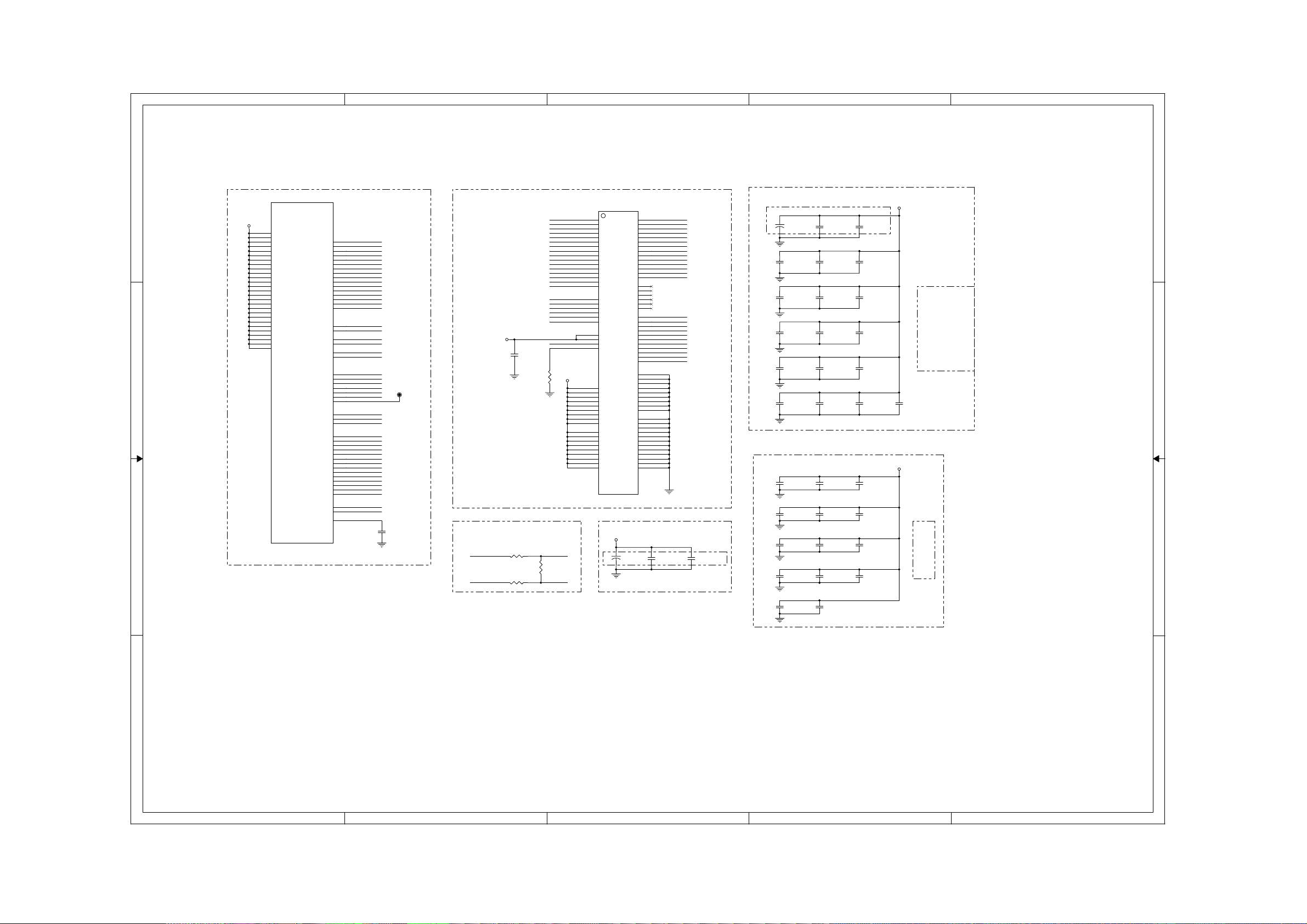
A
Main Board Circuit Diagram: AUDIO DAC
6-12
6-12
B
C
D
E
1 1
2 2
3 3
1.1V
J11
J14
J15
J17
J9
K10
K14
K16
L17
L9
M10
M16
N17
N9
P10
P16
R17
R9
T10
T12
T14
T16
U11
U13
U15
U17
U9
U100B
DVCC10_K
DVCC10_K
DVCC10_K
DVCC10_K
DVCC10_K
DVCC10_K
DVCC10_K
DVCC10_K
DVCC10_K
DVCC10_K
DVCC10_K
DVCC10_K
DVCC10_K
DVCC10_K
DVCC10_K
DVCC10_K
DVCC10_K
DVCC10_K
DVCC10_K
DVCC10_K
DVCC10_K
DVCC10_K
DVCC10_K
DVCC10_K
DVCC10_K
DVCC10_K
DVCC10_K
MT8550-DDR3-BGA492-090924
RDQ0_B
RDQ1_B
RDQ2_B
RDQ3_B
RDQ4_B
RDQ5_B
RDQ6_B
RDQ7_B
RDQ8_B
RDQ9_B
RDQ10_B
RDQ11_B
RDQ12_B
RDQ13_B
RDQ14_B
RDQ15_B
RDQM0_B
RDQM1_B
RDQS0_B
RDQS0__B
RDQS1_B
RDQS1__B
RODT_B
RCAS__B
RRAS__B
RCS__B
RWE__B
RCKE_B
RRESET_B
RBA0_B
RBA1_B
RBA2_B
RA0_B
RA1_B
RA2_B
RA3_B
RA4_B
RA5_B
RA6_B
RA7_B
RA8_B
RA9_B
RA10_B
RA11_B
RA12_B
RA13_B
RCLK0_B
RCLK0__B
RVREF_3
U21
U20
T24
T25
M20
M23
M22
M21
R22
R23
P23
P22
P20
R20
R21
P21
T21
T20
P24
P25
N25
N24
AE24
AD23
AC23
AD24
AE25
V21
Y25
AD25
U22
AC22
AB23
V22
AC25
AC24
V23
AA23
U24
Y22
U25
Y23
W24
U23
W25
Y24
M24
M25
R19
B_DQ0
B_DQ1
B_DQ2
B_DQ3
B_DQ4
B_DQ5
B_DQ6
B_DQ7
B_DQ8
B_DQ9
B_DQ10
B_DQ11
B_DQ12
B_DQ13
B_DQ14
B_DQ15
B_DQM0
B_DQM1
B_DQS0
B_DQS0#
B_DQS1
B_DQS1#
B_ODT
B_CAS#
B_RAS#
B_CS#
B_WE#
B_CKE
B_RRESET#
B_BA0
B_BA1
B_BA2
B_RA0
B_RA1
B_RA2
B_RA3
B_RA4
B_RA5
B_RA6
B_RA7
B_RA8
B_RA9
B_RA10
B_RA11
B_RA12
B_RA13
B_CLK0
B_CLK0#
DDR_VREF
C234
0.1uF/25V
R19
TP200
DDR
CHB
DDR_VREF
DDRB CLK
B_CLK0#
R202 0
B_CLK0 D_CLK2
R203 0
DDR_VREF
C272
0.1uF/25V
M8/H1
D_CLK2#
R200
100/1%
B_DQ0
B_DQ6
B_DQ3
B_DQ5
B_DQ1
B_DQ4
B_DQ2
B_DQ7
B_DQ12
B_DQ11
B_DQ13
B_DQ10
B_DQ14
B_DQ8
B_DQ15
B_DQ9
B_DQS1
B_DQS1#
B_DQS0
B_DQS0#
B_DQM1
B_DQM0
B_RRESET#
R201
1.5V
240
U203
E3
DQ0
F7
F2
F8
H3
H8
G2
H7
D7
C3
C8
C2
A7
A2
B8
A3
C7
B7
F3
G3
D3
E7
H1
M8
T2
L8
A1
A8
C1
C9
D2
E9
F1
H2
H9
B2
D9
G7
K2
K8
N1
N9
R9
R1
DECA refer MT8550
A0
DQ1
A1
DQ2
A2
DQ3
A3
DQ4
A4
DQ5
A5
DQ6
A6
DQ7
A7
DQ8
A8
DQ9
A9
DQ10
A10/AP
DQ11
A11
DQ12
A12/BC#
DQ13
A13
DQ14
NC_0
DQ15
NC_1
NC_2
UDQS
NC_3
UDQS#
NC_4
LDQS
NC_6
LDQS#
UDM
BA0
LDM
BA1
BA2
CK
VREFDQ
CK#
CS#
VREFCA
RESET#
CAS#
ODT
ZQ
RAS#
WE#
CKE
VSSQ_0
VSSQ_1
VSSQ_2
VDDQ_0
VSSQ_3
VDDQ_1
VSSQ_4
VDDQ_2
VSSQ_5
VDDQ_3
VSSQ_6
VDDQ_4
VSSQ_7
VDDQ_5
VSSQ_8
VDDQ_6
VSS_0
VDDQ_7
VSS_1
VDDQ_8
VSS_2
VDD_0
VSS_3
VDD_1
VSS_4
VSS_5
VDD_2
VDD_3
VSS_6
VDD_4
VSS_7
VDD_5
VSS_8
VSS_9
VDD_6
VSS_10
VDD_8
VSS_11
VDD_7
IC DDR3 x16 FBGA-96
1.5V
+
CE202
220uF/16V
N3
P7
P3
N2
P8
P2
R8
R2
T8
R3
L7
R7
N7
T3
J1
J9
L1
L9
M7
T7
M2
N8
M3
J7
K7
L2
K3
K1
J3
L3
K9
B1
B9
D1
D8
E2
E8
F9
G1
G9
A9
B3
E1
G8
J2
J8
M1
M9
P1
P9
T1
T9
B_RA0
B_RA1
B_RA2
B_RA3
B_RA4
B_RA5
B_RA6
B_RA7
B_RA8
B_RA9
B_RA10
B_RA11
B_RA12
B_RA13
B_BA0
B_BA1
B_BA2
D_CLK2
D_CLK2#
B_CS#
B_CAS#
B_ODT
B_RAS#
B_WE#
B_CKE
1.5V
POWER
C228
0.1uF/25V
MAIN POWER
C282
0.01uF/25V
IC 1.1V POWER C
MAIN POWER
+
CE205
470uF/16V
C223
0.1uF/25V
C202
0.1uF/25V
T12/U13 J 17 R9
C222
0.1uF/25V
C219
0.1uF/25V
J11 J9/K10 N9/P10
C231
0.1uF/25V
C207
0.01uF/25V
C203
0.1uF/25V
C208
0.1uF/25V
C211
0.1uF/25V
C220
0.1uF/25V
C232
0.1uF/25V
DDRB 1.5V POWER C
C273
0.1uF/25V
A8
C283
0.1uF/25V
E9
C240
0.1uF/25V
C1/D2 H2/K2/F1
C238
0.1uF/25V
C215
0.1uF/25V
A1
C230
0.1uF/25V
C236
0.1uF/25V
N9
C237
0.1uF/25V
R9 C9/D9G7
C206
0.1uF/25V
C201
0.1uF/25V
J14/K14T16/U17J15
C209
0.1uF/25V
C212
0.1uF/25V
K16/L17P16/R17T14/U15
C221
0.1uF/25V
C233
0.1uF/25V
U9T10/U11M16/N17
C269
0.1uF/25V
N1
C239
0.1uF/25V
B2H9
C241
0.1uF/25V
C229
0.1uF/25V
1.1V
1.5V
C227
0.1uF/25V
L9/M10
A1/A8
B2
C1/C9
D2/D9
E9
F1
G7
H2/H9
K2/K8
N1/N9
R1/R9
J9/J11/J14/J15/J17
K10/K14/K16
L9/L17
M10/M16
N9/N17
P10/P16
R9/R17
T10/T12/T14/T16
U9/U11/U13/U15/U17
4 4
A
C270
0.1uF/25V
R1 K8
B
C
C235
0.1uF/25V
D
E
Page 32
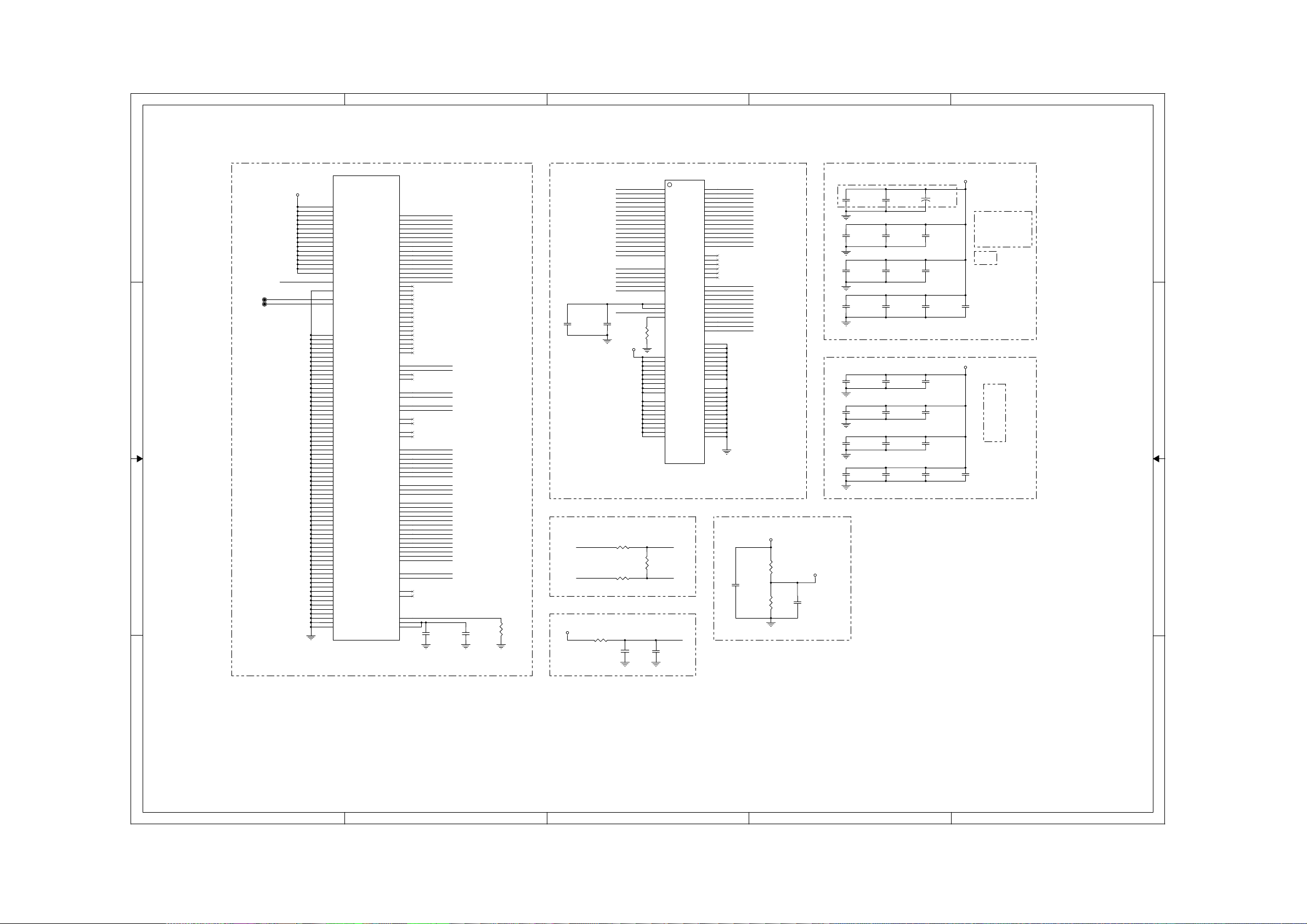
A
Main Board Circuit Diagram: MT8550 FE
6-13
6-13
B
C
D
E
U100A
1 1
TP101
TP102
2 2
3 3
1.5V
AVDD12_MEMPLL
A_TP_MEMPLL
A_TN_MEMPLL
AB20
DVCC18_IO_1
AB21
DVCC18_IO_1
AC10
DVCC18_IO_1
AC13
DVCC18_IO_1
AC17
DVCC18_IO_1
AC7
DVCC18_IO_1
N18
DVCC18_IO_1
N23
DVCC18_IO_1
T18
DVCC18_IO_1
T23
DVCC18_IO_1
V12
DVCC18_IO_1
V14
DVCC18_IO_1
V16
DVCC18_IO_1
V18
DVCC18_IO_1
V9
DVCC18_IO_1
W23
DVCC18_IO_1
Y21
AVDD12_MEMPLL
W21
AVSS12_MEMPLL
AB25
TP_MEMPLL
AB24
TN_MEMPLL
E21
DGND
J10
DGND
F21
DGND
J16
DGND
K9
DGND
K11
DGND
K13
DGND
K15
DGND
K17
DGND
L10
DGND
L11
DGND
L12
DGND
L13
DGND
L14
DGND
L15
DGND
L16
DGND
M11
DGND
M12
DGND
M13
DGND
M14
DGND
M15
DGND
M17
DGND
AA7
DGND
M9
DGND
N10
DGND
N11
DGND
N12
DGND
N13
DGND
N14
DGND
N15
DGND
N16
DGND
N22
DGND
P11
DGND
P12
DGND
P13
DGND
P14
DGND
P15
DGND
P17
DGND
Y6
DGND
P9
DGND
R10
DGND
R11
DGND
R12
DGND
R13
DGND
R14
DGND
R15
DGND
R16
DGND
T11
DGND
T13
DGND
T15
DGND
T17
DGND
T22
DGND
D22
DGND
T9
DGND
U10
DGND
U12
DGND
U14
DGND
U16
DGND
W22
DGND
Y8
DGND
AA20
DGND
AB10
DGND
AB13
DGND
AB17
DGND
AA6
DGND
AB7
DGND
AC21
DGND
MT8550-DDR3-BGA492-090924
RDQ0
RDQ1
RDQ2
RDQ3
RDQ4
RDQ5
RDQ6
RDQ7
RDQ8
RDQ9
RDQ10
RDQ11
RDQ12
RDQ13
RDQ14
RDQ15
RDQ16
RDQ17
RDQ18
RDQ19
RDQ20
RDQ21
RDQ22
RDQ23
RDQ24
RDQ25
RDQ26
RDQ27
RDQ28
RDQ29
RDQ30
RDQ31
RDQM0
RDQM1
RDQM2
RDQM3
RDQS0
RDQS0_
RDQS1
RDQS1_
RDQS2
RDQS2_
RDQS3
RDQS3_
RODT
RCAS_
RRAS_
RCS_
RWE_
RCKE
RRESET
RBA0
RBA1
RBA2
RA0
RA1
RA2
RA3
RA4
RA5
RA6
RA7
RA8
RA9
RA10
RA11
RA12
RA13
RCLK0
RCLK0_
RCLK1
RCLK1_
REXTDN
RVREF_2
RVREF_1
AE16
AD16
AC16
AB16
AD21
AE21
AC20
Y18
AE17
AD17
AC18
AA17
AA19
AC19
AA18
AB19
AD3
AD4
AE3
AE4
AA10
Y10
Y9
AA9
AB6
AB5
AC5
AC6
AE9
AD9
AC9
AB9
Y17
AB18
AB8
AC8
AD19
AE19
AE20
AD20
AD6
AE6
AE7
AD7
AB11
AA11
Y11
AC11
AE12
AA14
Y14
AD12
AC15
AC12
AA12
AB15
AE13
AB12
AA15
Y12
Y16
AD13
AA16
AC14
AD14
Y15
AE14
AB14
AD22
AE22
AD10
AE10
AE23
Y19
W12
A_DQ0
A_DQ1
A_DQ2
A_DQ3
A_DQ4
A_DQ5
A_DQ6
A_DQ7
A_DQ8
A_DQ9
A_DQ10
A_DQ11
A_DQ12
A_DQ13
A_DQ14
A_DQ15
A_DQM0
A_DQM1
A_DQS0
A_DQS0#
A_DQS1
A_DQS1#
A_ODT
A_CAS#
A_RAS#
A_CS#
A_WE#
A_CKE
A_RRESET#
A_BA0
A_BA1
A_BA2
A_RA0
A_RA1
A_RA2
A_RA3
A_RA4
A_RA5
A_RA6
A_RA7
A_RA8
A_RA9
A_RA10
A_RA11
A_RA12
A_RA13
A_CLK0
A_CLK0#
REXTUN
DDR_VREF
C102
0.1uF/25V
Y19
C103
0.1uF/25V
W12
R111
100/1%
DDR
C135
0.1uF/25V
A_DQ0
A_DQ7
A_DQ1
A_DQ6
A_DQ3
A_DQ5
A_DQ2
A_DQ4
A_DQ13
A_DQ15
A_DQ12
A_DQ9
A_DQ11
A_DQ8
A_DQ14
A_DQ10
A_DQS1
A_DQS1#
A_DQS0
A_DQS0#
A_DQM1
A_DQM0
DDR_VREF
A_RRESET#
1.5V
CHA
C132
0.1uF/25V
H1 M8
DDRA CLK
A_CLK0#
R105 0
R108 0
DDR PLL POWER C
1.2V
R112 0
C115
NC
U104
E3
DQ0
DQ1
DQ2
DQ3
DQ4
DQ5
DQ6
DQ7
DQ8
DQ9
DQ10
DQ11
DQ12
DQ13
DQ14
DQ15
UDQS
UDQS#
LDQS
LDQS#
UDM
LDM
VREFDQ
VREFCA
RESET#
ZQ
VDDQ_0
VDDQ_1
VDDQ_2
VDDQ_3
VDDQ_4
VDDQ_5
VDDQ_6
VDDQ_7
VDDQ_8
VDD_0
VDD_1
VDD_2
VDD_3
VDD_4
VDD_5
VDD_6
VDD_8
VDD_7
A10/AP
A12/BC#
NC_0
NC_1
NC_2
NC_3
NC_4
NC_6
CAS#
ODT
RAS#
WE#
CKE
VSSQ_0
VSSQ_1
VSSQ_2
VSSQ_3
VSSQ_4
VSSQ_5
VSSQ_6
VSSQ_7
VSSQ_8
VSS_0
VSS_1
VSS_2
VSS_3
VSS_4
VSS_5
VSS_6
VSS_7
VSS_8
VSS_9
VSS_10
VSS_11
A0
A1
A2
A3
A4
A5
A6
A7
A8
A9
A11
A13
BA0
BA1
BA2
CK
CK#
CS#
F7
F2
F8
H3
H8
G2
H7
D7
C3
C8
C2
A7
A2
B8
A3
C7
B7
F3
G3
D3
E7
H1
M8
T2
L8
R114
240
A1
A8
C1
C9
D2
E9
F1
H2
H9
B2
D9
G7
K2
K8
N1
N9
R9
R1
IC DDR3 x16 FBGA-96
DECA refer MT8550
D_CLK0#
R106
100/1%
D_CLK0A_CLK0
AVDD12_MEMPLL
C116
0.1uF/25V
A_RA0
N3
A_RA1
P7
A_RA2
P3
A_RA3
N2
A_RA4
P8
A_RA5
P2
A_RA6
R8
A_RA7
R2
A_RA8
T8
A_RA9
R3
A_RA10
L7
A_RA11
R7
A_RA12
N7
A_RA13
T3
J1
J9
L1
L9
M7
T7
A_BA0
M2
A_BA1
N8
A_BA2
M3
D_CLK0
J7
D_CLK0#
K7
A_CS#
L2
A_CAS#
K3
A_ODT
K1
A_RAS#
J3
A_WE#
L3
A_CKE
K9
B1
B9
D1
D8
E2
E8
F9
G1
G9
A9
B3
E1
G8
J2
J8
M1
M9
P1
P9
T1
T9
DDR
1.5V
VREF
R109
100/1%
C101
0.1uF/25V
DDR_VREF
R110
100/1%
IC 1.5V POWER C
MAIN POWER
C142
0.1uF/25V
C129
0.1uF/25V
IC MID
C106
0.1uF/25V
W23
C110
0.1uF/25V
AC13
DDRA 1.5V POWER C
C143
0.1uF/25V
K8
C128
0.1uF/25V
C141
0.1uF/25V
C140
0.1uF/25V
DDR_VREF
C136
0.1uF/25V
²?
俀㕈㔼
C118
0.1uF/25V
C104
0.1uF/25V
AC7/AC10
C134
0.1uF/25V
N23
C137
0.1uF/25V
T23
C157
0.1uF/25V
H9 D9/E9
C144
0.1uF/25V
R1
C160
0.1uF/25V
C146
0.1uF/25V
+
CE100
220uF/16V
C105
0.1uF/25V
V16/V18
C107
0.1uF/25V
V9/V12/V14
C133
0.1uF/25V
C158
0.1uF/25V
C117
0.1uF/25V
G7H2/K2
C161
0.1uF/25V
R9N9F1
C139
0.1uF/25V
1.5V
T18/T23
N18/N23
AB20/AB21
AC7/AC10/AC13/AC17
V9/V12/V14/V16/V18
W23
AC17
C125
0.1uF/25V
AB20/AB21T18/N18
1.5V
C159
0.1uF/25V
A8/C9A1/B2N1C1/D2
A1/A8
B2
C1/C9
D2/D9
E9
F1
G7
H2/H9
K2/K8
N1/N9
R1/R9
4 4
A
B
C
D
E
Page 33
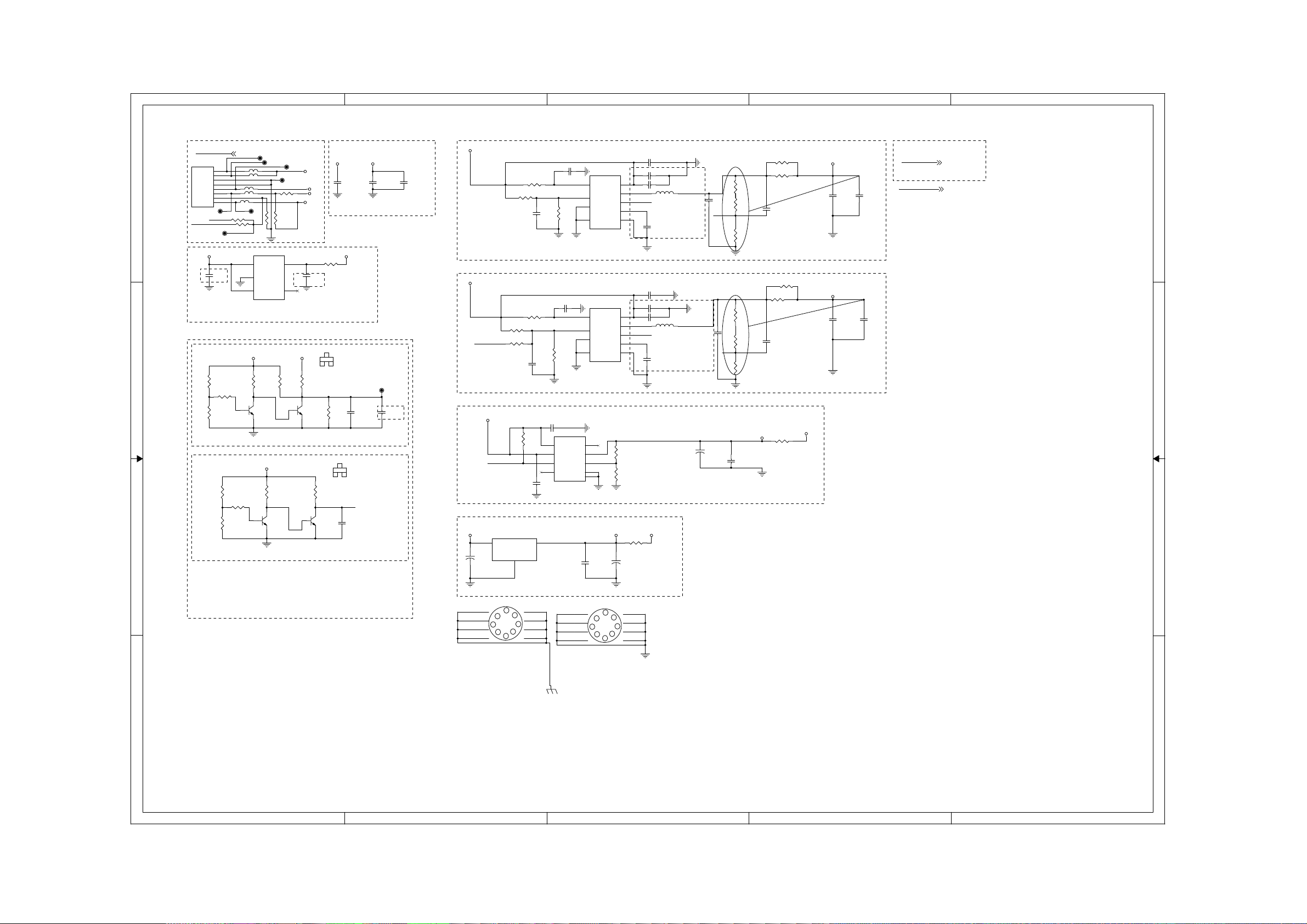
A
Main Board Circuit Diagram: FE MOTOR DRIVER
6-14
6-14
B
C
D
E
C9
0.1uF/25V
C43
0.1uF/25V
CNT
RESET#
OPWRSB
RESET#
OPWRSB
(7)
VCC
VCC
VCC
VCC1
FB706 FB10/2A
1
1
FB707 FB10/2A
2
2
3
3
4
4
FB708 FB10/2A
5
5
FB711 FB10/2A
6
6
7
1 1
2 2
3 3
7
8
8
J18PIN/2.5MM
N12V
5V_STBY
OPWRSB
R22 0R/NC
ON
mark power net at connector bot
5V_STBY
close to DC/DC
C3
2.2uF/10V
R27
1.5K/1%
R30 100
R34
2.7K
VCC R/R to Q3.b
5.000V 0.772V
4.532V 0.700V
3.885V 0.600V
3.237V 0.500V
VCC R/R to Q1.b
5.000V 0.772V
4.532V 0.700V
3.885V 0.600V
3.237V 0.500V
FB712 FB10/2A
5VS
R21 0R/NC
U5
1
VIN
2
GND
EN3NC
G9091-330T11U
SOT-25/SMD
5V_STBY
R33
15K/1%
0603
R35 100
R28
27K
0603
12V_P
GND
R16 0R
R19
R18
0R
0R/NC
POWER
CONNECTOR
5
VOUT
close to LDO
4
µ DO/ 100UA/ 300MA
ࠨǂ㞆 オ䖭 ᐕ
3.3V_STBY
R36
R42
33K/NC
3.3K
Q3
3DG3904M
VCC
R31
3.3K
Q1
3DG3904M
VCC
12V_P
N12V
5V_STBY
R13 0
C4
4.7uF/10V
1
2N3904
R32
10K
Q4
3DG3904M
2
C
EB
1
2N3904
R38
100K
DC_EN
Q2
3DG3904M
12V_P
3.3V_STBY
3
R40
100K/NC
C
C20
4.7uF/16V
2
3
EB
100MA(Max)
STBY
3.3V
POWER
RESET#
C18
10uF/10V
C38
0.1uF/50V/X7R
VCC
RESET
CIRCUIT
TP1
DC disable
CIRCUIT
C925
22uF/10V
0.1uF/25V
close to IC
C46
0.1uF/25V
C45
VCC
VCC
3.3V
+
CE904
100uF/16V
1.1V_EN
VCC
3
R1 100 K/NC
R39 30K/NC
DC_EN
IN
R12 10
R3 2.4K/1%
C26
0.1uF/25V
R24 10
R6
10K/NC
OUT
ADJ
1
U1
AS1117
C29
0.1uF/16V/NC
C14 10uF/10V
3
2
1
C5
10uF/16V/50V/X7R
1A Regulator
2
C31
0.1uF/25V
1.1V_EN
R20
10K
C30
0.1uF/25V
DC_EN
R11
20K/NC
U3 G966A
VPP4NC
VIN
VEN
ADJ
POK
GND
U2
1
VCC
5
EN
3
GND
9
TP
G5693
U4
1
VCC
5
EN
3
GND
9
TP
G5693
5
6
VO
7
8
9
TP
C41
0.1uF/25V
C33
0.1uF/25V
Close to DC-DC
C16
10uF/10V
L2 2.2uH/3A
DC Current: 4.1A
Saturation Current: 6.4A
1.1V_FB
DC resistor: 15mOHM
C34
0.1uF/25V
C15
10uF/10V
PGND
8
VIN
7
LX
4
FB
2
REF
6
(pin to pin with G5627) 3.2A
C32
0.1uF/25V
DC Current: 4.1A
Saturation Current: 6.4A
DC resistor: 15mOHM
C35
0.1uF/25V
Close to DC-DC
PGND
C11 10uF/10V
C12 10uF/10V
8
VIN
LX
FB
REF
7
1.5V_FB
4
2
6
L1 2.2uH/3A
behind of Caps
R922
330
C8
22uF/10V
1.1V_FB
AIM 1.15V: 0.8*(6.65+15)/15=1.155V
AIM 1.2V: 0.8*(7.87+15)/15=1.22V
↕ ᴹⴱ⭥⁑ᔿ
behind of Caps
C17
22uF/10V
1.5V_FB
AIM 1.5V: 0.8*(13.3+15)/15=1.509V
(pin to pin with G5627) 3.2A
R9
15K/1%
AIM 3.3V: 0.8*(15+4.75)/4.75=3.326V
R29
4.7K/1%
+
CE905
100uF/16V
A1.2V
R17
0
1.2V
1.2V
POWER
+
CE903
100uF/16V
C44
0.1uF/25V
R930 0
R926 0
R2
C1
5.6K/1%
0.1uF/25V
R7
15K/1%
R934 0
R927 0
R928
560
R4
C2
13K/1%
0.1uF/25V
R5
15K/1%
↕ ᴹⴱ⭥⁑ᔿ
3.3V
700MA
R10 0
3.3V
POWER
A3.3V
1.1V
POWER
1.1V
C10
22uF/10V
1.5V
POWER
1.5V
1200MA
C13
22uF/10V
4 4
A
M1
1
2
3
4
1
2
3
4
100115/SO
8
8
7
7
6
6
5
5
M
B
1
2
3
4
100115/SO
M2
1
2
3
4
8
8
7
7
6
6
5
5
C
D
E
Page 34
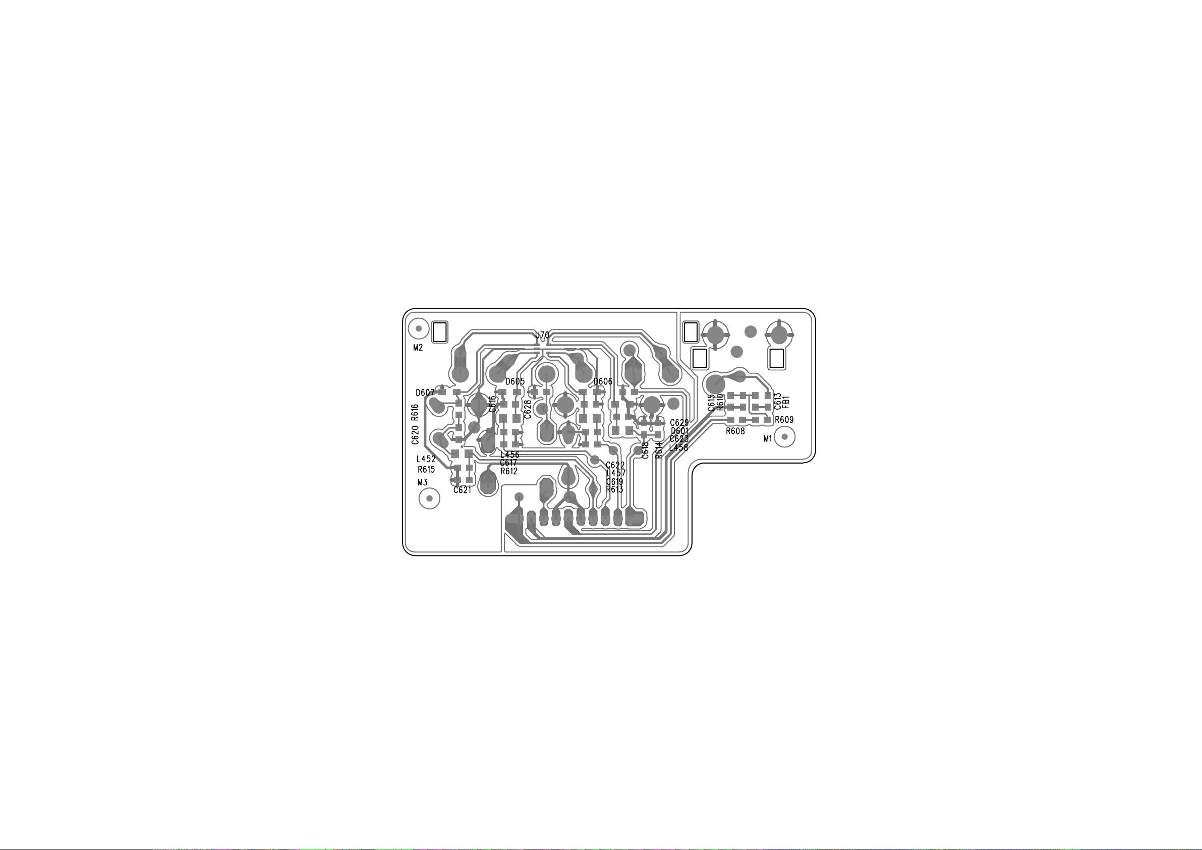
AV BOARD - PCB LAYOUT
6-15
6-15
Page 35
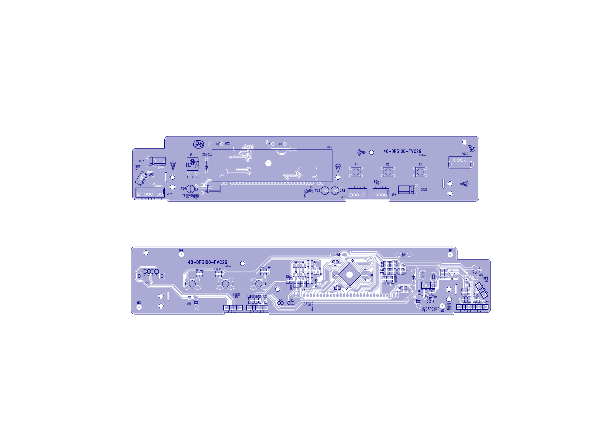
6-16 6
Front Board Print-layout (Top and Bottom side):
-16
Page 36
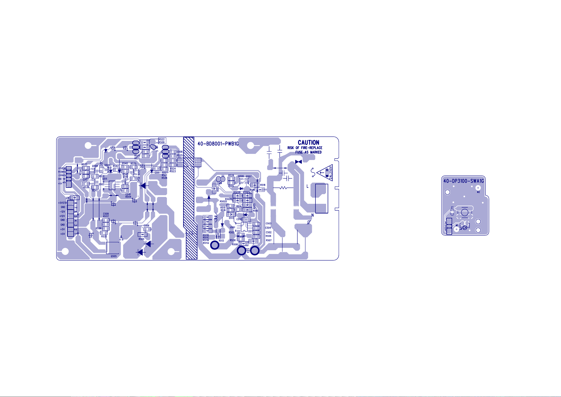
6-17 6
Power Board Print-layout (Bottom side): Switch Board Print-layout (Bottom side):
-17
Page 37
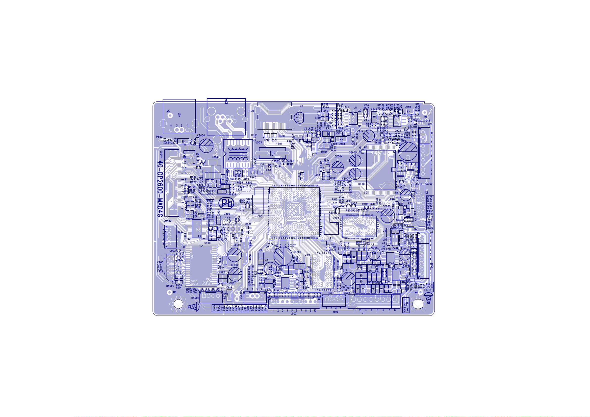
6-18
6-18
Main Board Print-layout(Top Side):
Page 38
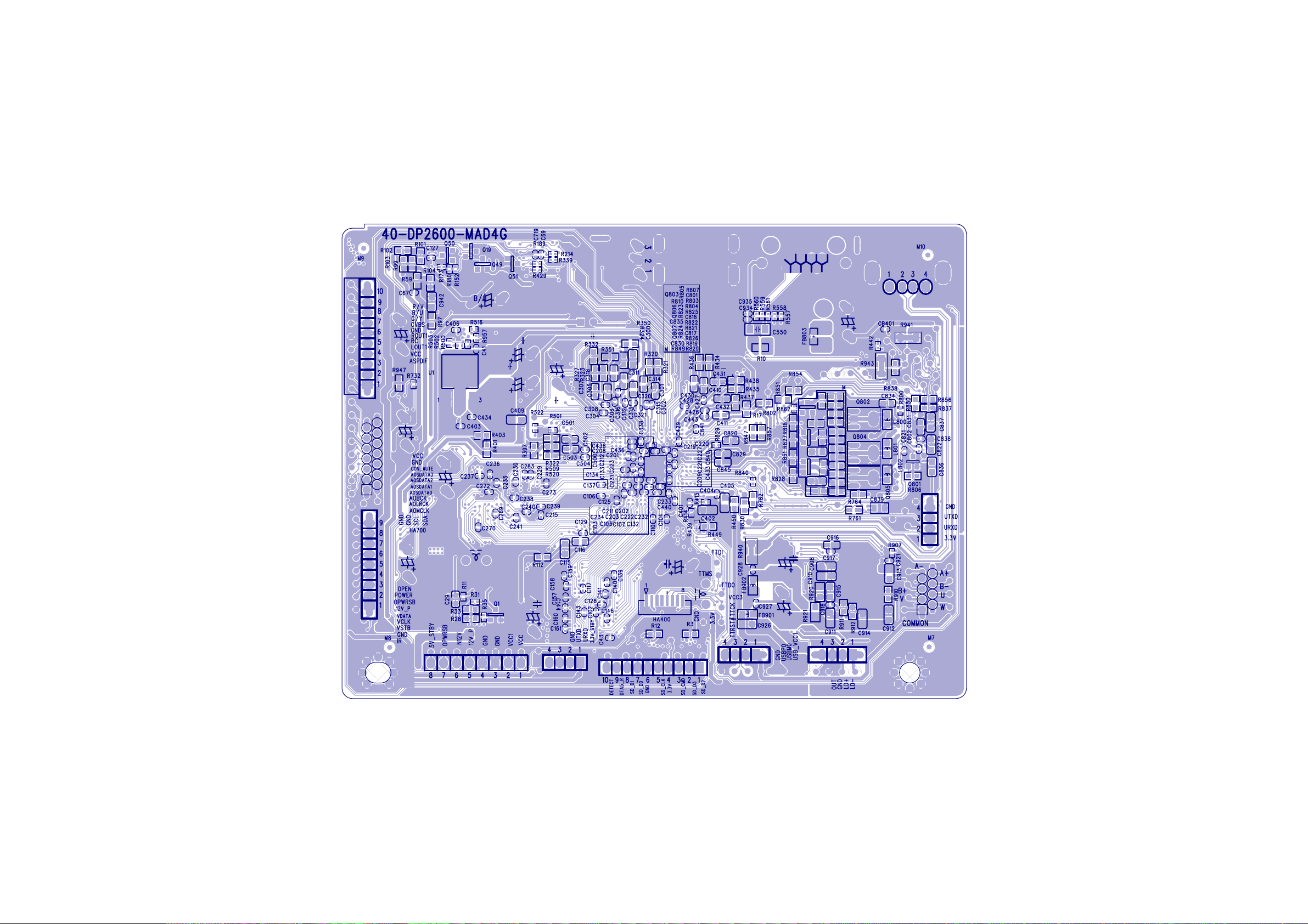
6-19
6-19
Main Board Print-layout(Bottom Side):
Page 39
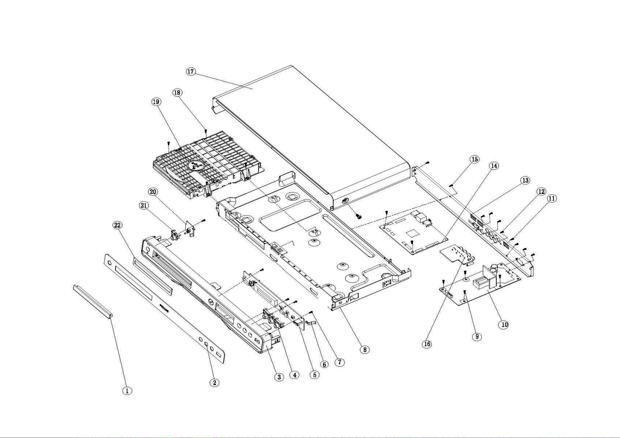
7-1 7-1
Exploded view for BDP3100/12/05/51/55/93/96/98/79/X78 ,BDP3080/98
It is a general mechanical exploded view for BDP3100,BDP3080/98 pls refer to the model set for detailed information.ASSY1 includes components:2.3.4.21.22
Page 40

8-1
REVISION LIST
Version 1.0
* Initial release for BDP3100/12/05/51/55/79/93/96/98/x78 (MKII version, S/N with KX1Bxxxxxxxxxx
or SM1Bxxxxxxxxxx)
Version 1.1
* BDP3080/98 added.
Version 1.2
* Page 7-1 Mechanical Exploded View updated.
 Loading...