

Philips bcy 88 DATASHEETS
DISCRETE SEMICONDUCTORS
DATA SH EET
M3D126
BCY87; BCY88; BCY89
NPN general purpose transistors
Product specification
Supersedes data of September 1994
1997 Jun 20
File under Discrete Semiconductors, SC04
Philips Semiconductors Product specification
NPN general purpose transistors BCY87; BCY88; BCY89
FEATURES
• Low current (max. 30 mA)
• Low voltage (max. 45 V).
APPLICATIONS
• Differential amplifier applications in general industrial
service e.g. instrumentation and control
• The BCY87 and BCY88 are intended for use in
pre-stages of differential amplifiers where low offset, low
drift and low noise are of prime importance
• The BCY89 is intended for use in second stages of
differential amplifiers, long-tailed pairs and more general
applications.
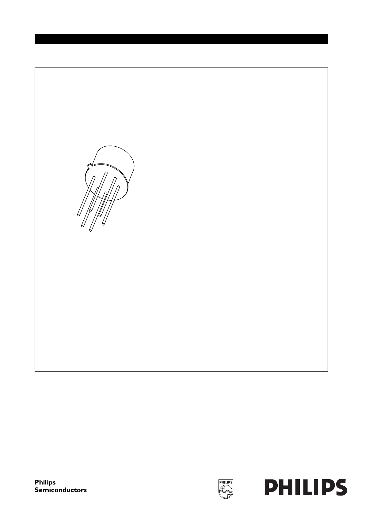
DESCRIPTION
Matched dual NPN transistors in a TO-71; SOT31 metal
package. Products are divided into 3 types according to
their matching accuracy.
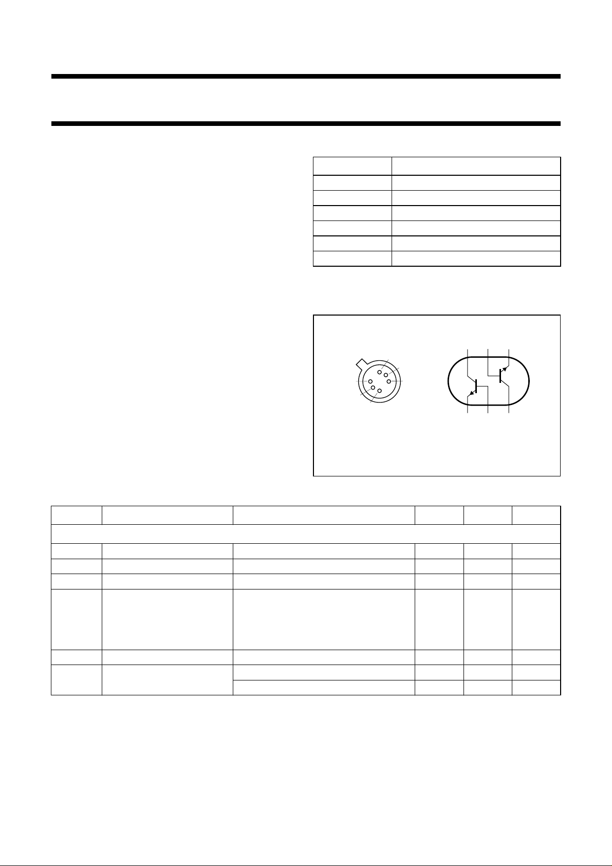
PINNING
(1)
PIN
DESCRIPTION
1 emitter TR1
2 emitter TR2
3 collector TR2
4 basis TR2
5 basis TR1
6 collector TR1
Note
1. All leads insulated from the case.
handbook, halfpage
1
2
6
5
4
3
MAM351
TR1
624
TR2
135
Fig.1 Simplified outline (TO-71; SOT31)
and symbol.
QUICK REFERENCE DATA
SYMBOL PARAMETER CONDITIONS MIN. MAX. UNIT
Per transistor
V
V
P
h
h
f
T
CBO
CEO
tot
FE
FE
collector-base voltage open emitter − 45 V
collector-emitter voltage open base − 40 V
total power dissipation T
≤ 25 °C − 150 mW
amb
DC current gain VCE=10V
BCY87 I
BCY88 I
BCY89 I
=5µA80−
C
= 500 µA 120 600
C
= 10 mA 100 600
C
DC current gain IC=50µA; VCE= 10 V 100 450
transition frequency IC= −50 µA; VCE= 10 V; f = 100 MHz 10 − MHz
I
= −500 µA; VCE= 10 V; f = 100 MHz 50 − MHz
C
1997 Jun 20 2

Philips Semiconductors Product specification
NPN general purpose transistors BCY87; BCY88; BCY89
LIMITING VALUES
In accordance with the Absolute Maximum Rating System (IEC 134).
SYMBOL PARAMETER CONDITIONS MIN. MAX. UNIT
V
CBO
V
CEO
V
EBO
I
C
P
tot
T
stg
T
j
THERMAL CHARACTERISTICS
SYMBOL PARAMETER CONDITIONS VALUE UNIT
R
th j-a
collector-base voltage open emitter − 45 V
collector-emitter voltage open base − 40 V
emitter-base voltage open collector − 5V
collector current (DC) − 30 mA
total power dissipation T
≤ 25 °C − 150 mW
amb
storage temperature −65 +150 °C
junction temperature − 175 °C
thermal resistance from junction to ambient in free air 1 K/mW
CHARACTERISTICS
T
=25°C unless otherwise specified.
amb
SYMBOL PARAMETER CONDITIONS MIN. TYP. MAX. UNIT
Per transistor
I
CBO
collector cut-off current IE= 0; VCB=20V; T
amb
=90°C
BCY87 −−5nA
BCY88 −−20 nA
I
CBO
collector cut-off current IE= 0; VCB=20V
BCY89 −−10 nA
h
FE
h
FE
C
c
f
T
DC current gain VCE=10V
BCY87 I
BCY88 I
BCY89 I
=5µA80−−
C
= 500 µA 120 − 600
C
= 10 mA 100 − 600
C
DC current gain IC=50µA; VCE= 10 V 100 − 450
collector capacitance IE=ie= 0; VCB= 10 V; f = 1 MHz −−3.5 pF
transition frequency IE= −50 µA; VCE=10V;
10 −−MHz
f = 100 MHz
I
= −500 µA; VCE=10V;
E
50 −−MHz
f = 100 MHz
F noise figure I
= 200 µA; VCE=5V;
C
−−4dB
RS=2kΩ; f = 10 Hz to 15.7 kHz
F noise figure I
BCY87 −−4dB
= 200 µA; VCE=5V;
C
RS=2kΩ; f = 1 kHz; B = 200 Hz
BCY88; BCY89 −−5dB
1997 Jun 20 3
 Loading...