

Philips BCY59, BCY58 Datasheet
DISCRETE SEMICONDUCTORS
DATA SH EET
M3D125
BCY58; BCY59
NPN switching transistors
Product specification
Supersedes data of September 1994
File under Discrete Semiconductors, SC04
1997 Jun 17
Philips Semiconductors Product specification
NPN switching transistors BCY58; BCY59
FEATURES
• Low current (max. 100 mA)
• Low voltage (max. 45 V).
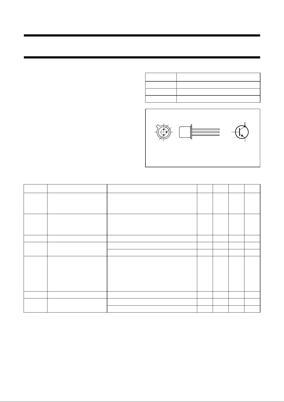
PINNING
PIN DESCRIPTION
1 emitter
2 base
APPLICATIONS
3 collector, connected to case
• Switching and amplification.
DESCRIPTION
NPN switching transistor in a TO-18 metal package.
PNP complements: BCY78 and BCY79.
handbook, halfpage
1
3
2
2
MAM264
3
1
Fig.1 Simplified outline (TO-18) and symbol.
QUICK REFERENCE DATA
SYMBOL PARAMETER CONDITIONS MIN. TYP. MAX. UNIT
V
CBO
collector-base voltage open emitter
BCY58 −−32 V
BCY59 −−45 V
V
CEO
collector-emitter voltage open base
BCY58 −−32 V
BCY59 −−45 V
I
C
P
tot
h
FE
collector current (DC) −−100 mA
total power dissipation T
≤ 45 °C −−340 mW
amb
T
≤ 45 °C −−1W
case
DC current gain IC= 2 mA; VCE=5V
BCY58/VII; BCY59/VII 120 170 220
BCY58/VIII; BCY59/VIII 180 250 310
BCY58/IX; BCY59/IX 250 350 460
BCY58/X; BCY59/X 380 500 630
f
T
t
off
transition frequency IC= 10 mA; VCE= 5 V; f = 100 MHz 150 −−MHz
turn-off time I
= 10 mA; I
Con
= 100 mA; I
I
Con
Bon
Bon
= 1 mA; I
= 10 mA; I
= −1mA − 480 800 ns
Boff
= −10 mA − 450 800 ns
Boff
1997 Jun 17 2
Philips Semiconductors Product specification
NPN switching transistors BCY58; BCY59
LIMITING VALUES
In accordance with the Absolute Maximum Rating System (IEC 134).
SYMBOL PARAMETER CONDITIONS MIN. MAX. UNIT
V
CBO
V
CEO
V
EBO
I
C
I
CM
I
BM
P
tot
T
stg
T
j
T
amb
collector-base voltage open emitter
BCY58 − 32 V
BCY59 − 45 V
collector-emitter voltage open base
BCY58 − 32 V
BCY59 − 45 V
emitter-base voltage open collector − 7V
collector current (DC) − 100 mA
peak collector current − 200 mA
peak base current − 200 mA
total power dissipation T
≤ 45 °C − 340 mW
amb
T
≤ 45 °C − 1W
case
storage temperature −65 +150 °C
junction temperature − 200 °C
operating ambient temperature −65 +150 °C
THERMAL CHARACTERISTICS
SYMBOL PARAMETER CONDITIONS VALUE UNIT
R
R
th j-a
th j-c
thermal resistance from junction to ambient in free air 450 K/W
thermal resistance from junction to case 150 K/W
CHARACTERISTICS
=25°C unless otherwise specified.
T
j
SYMBOL PARAMETER CONDITIONS MIN. TYP. MAX. UNIT
I
CBO
I
CBO
I
EBO
h
FE
collector cut-off current
BCY58 I
= 0; VCB=32V −−10 nA
E
= 0; VCB= 32 V; Tj= 150 °C −−10 µA
I
E
collector cut-off current
BCY59 I
= 0; VCB=45V −−10 nA
E
I
= 0; VCB= 45 V; Tj= 150 °C −−10 µA
E
emitter cut-off current IC= 0; VEB=5V −−10 nA
DC current gain IC=10µA; VCE=5V
BCY58/VII; BCY59/VII − 20 −
BCY58/VIII; BCY59/VIII 20 95 −
BCY58/IX; BCY59/IX 40 190 −
BCY58/X; BCY59/X 100 300 −
1997 Jun 17 3
 Loading...