

Page 1

DVD-Video Recorder DVD+RW Basic Engine
VAD8031
Contents Page Contents Page
1 Technical Specifications 2
2 Safety Instructions, Warnings and Notes 3
3 Directions for Use (No DFU necessary) 4
4 Mechanical Instructions 5
5 Service Modes, Error Codes and Fault Finding 8
6
Block Diagrams, Waveforms, Wiring Diagram 13
Block Diagram 13
7
Electrical Diagrams and Print-Layouts Diagram PWB
Servo Board: OPU Interface (Diagram 1) 14 28-29
Servo Board: Cheetah (Diagram 2
Servo Board: Laconic (Diagram 3) 16 28-29
Servo Board: Drivers (Diagram 4) 17 28-29
Servo Board: Centaurus (Diagram 5) 20 28-29
Servo Board: Power, Connectors (Diagram 6) 26 28-29
Servo Board: Tray Motor Connect.(Diagram 7) 27 28-29
8 Alignments 31
9 Circuit-, IC Descriptions and List
of Abbreviations 32
10 Electrical Parts List 47
) 15 28-29
©
Copyright 2003 Philips Consumer Electronics B.V. Eindhoven, The Netherlands.
All rights reserved. No part of this publication may be reproduced, stored in a
retrieval system or transmitted, in any form or by any means, electronic,
mechanical, photocopying, or otherwise without the prior permission of Philips.
Published by GH03 0395 Service PaCE Printed in the Netherlands Subject to modification EN 3122 785 13680
Page 2

EN 2 VAD 80311.
Technical Specifications and Connection Facilities
1. Technical Specifications and Connection Facilities
1.1 VAD8031 functionality:
• Loading of 8 cm and 12 cm discs by a motorized tray
• Disc type recognition and in case of a DVD+RW disc laser
power calibration
• Servo control for disc rotation, sledge movements, tilt,
focus and actuator position
• EFM+ encoding / decoding for DVD, and EFM decoding for
CD
• Writes and read DVD+RW discs and reads DVD, CD and
CD-R/RW discs
• Linking control, header insertion and sector number
updating at record
• Interfacing to the MPEG back-end for control and for data
• The back-end has to provide MPEG data processing, data
buffering, construction of logical format for Lead-in, Data
area and Lead-out part of the DVD+RW disc
1.2 Connections
The following interfaces are provided for connecting the drive
to the MPEG back-end Application:
• Power Connector: 4-pin supply interface
• IDE Connector: 40-pin command and data transfer
interface
IDE Bus selection:
• Jumper Selection: 6-pin IDE Bus selector
Attention: Jumper has to be in position "Master"
1.3 Read and Write Speeds
Type of Disc (Function) Disc Rotation Speed
Read Speed CD CAV 7x
Read Speed DVD CAV 4x
Write Speed DVD+RW
Write Speed DVD+R
ZCAV 2.4x
ZCAV 2.4x
Page 3
Safety Instructions, Warnings and Notes
2. Safety Instructions, Warnings and Notes
EN 3VAD 8031 2.
2.1 Safety Instructions
2.1.1 General Safety
Safety regulations require that during a repair:
• Connect the unit to the mains via an isolation transformer.
• Replace safety components, indicated by the symbol ,
only by components identical to the original ones. Any
other component substitution (other than original type) may
increase risk of fire or electrical shock hazard.
Safety regulations require that after a repair, you must return
the unit in its original condition. Pay, in particular, attention to
the following points:
• Route the wires/cables correctly, and fix them with the
mounted cable clamps.
• Check the insulation of the mains lead for external
damage.
• Check the electrical DC resistance between the mains plug
and the secondary side:
1. Unplug the mains cord, and connect a wire between
the two pins of the mains plug.
2. Set the mains switch to the 'on' position (keep the
mains cord unplugged!).
3. Measure the resistance value between the mains plug
and the front panel, controls, and chassis bottom.
4. Repair or correct unit when the resistance
measurement is less than 1 MΩ.
5. Verify this, before you return the unit to the customer/
user (ref. UL-standard no. 1492).
6. Switch the unit ‘off’, and remove the wire between the
two pins of the mains plug.
2.1.2 Laser Safety
This unit employs a laser. Only qualified service personnel may
remove the cover, or attempt to service this device (due to
possible eye injury).
2.2 Warnings
2.2.1 General
• All ICs and many other semiconductors are susceptible to
electrostatic discharges (ESD, symbol ). Careless
handling during repair can reduce life drastically. Make
sure that, during repair, you are at the same potential as
the mass of the set by a wristband with resistance. Keep
components and tools at this same potential. Available
ESD protection equipment:
– Complete kit ESD3 (small tablemat, wristband,
connection box, extension cable and earth cable) 4822
310 10671.
– Wristband tester 4822 344 13999.
• Be careful during measurements in the live voltage section.
The primary side of the power supply (pos. 1005), including
the heatsink, carries live mains voltage when you connect
the player to the mains (even when the player is 'off'!). It is
possible to touch copper tracks and/or components in this
unshielded primary area, when you service the player.
Service personnel must take precautions to prevent
touching this area or components in this area. A 'lightning
stroke' and a stripe-marked printing on the printed wiring
board, indicate the primary side of the power supply.
• Never replace modules, or components, while the unit is
‘on’.
2.2.2 Laser
• The use of optical instruments with this product, will
increase eye hazard.
• Only qualified service personnel may remove the cover or
attempt to service this device, due to possible eye injury.
• Repair handling should take place as much as possible
with a disc loaded inside the player.
• Text below is placed inside the unit, on the laser cover
shield:
Laser Device Unit
Type : Semiconductor laser
GaAlAs
Wavelength : 650 nm (DVD)
: 780 nm (VCD/CD)
Output Power : 20 mW (DVD+RW
writing)
: 0.8 mW (DVD
reading)
: 0.3 mW (VCD/CD
reading)
Beam divergence : 60 degree
Figure 2-1 Class 1 Laser Product
Note: Use of controls or adjustments or performance of
procedure other than those specified herein, may result in
hazardous radiation exposure. Avoid direct exposure to beam.
CAUTION VISIBLE AND INVISIBLE LASER RADIATION WHEN OPEN AVOID EXPOSURE TO BEAM
ADVARSEL SYNLIG OG USYNLIG LASERSTRÅLING VED ÅBNING UNDGÅ UDSÆTTELSE FOR STRÅLING
ADVARSEL SYNLIG OG USYNLIG LASERSTRÅLING NÅR DEKSEL ÅPNES UNNGÅ EKSPONERING FOR STRÅLEN
VARNING SYNLIG OCH OSYNLIG LASERSTRÅLNING NÄR DENNA DEL ÄR ÖPPNAD BETRAKTA EJ STRÅLEN
VARO! AVATTAESSA OLET ALTTIINA NÄKYVÄLLE JA NÄKYMÄTTÖMÄLLE LASER SÄTEILYLLE. ÄLÄ KATSO SÄTEESEEN
VORSICHT SICHTBARE UND UNSICHTBARE LASERSTRAHLUNG WENN ABDECKUNG GEÖFFNET NICHT DEM STRAHL AUSSETSEN
DANGER VISIBLE AND INVISIBLE LASER RADIATION WHEN OPEN AVOID DIRECT EXPOSURE TO BEAM
ATTENTION RAYONNEMENT LASER VISIBLE ET INVISIBLE EN CAS D'OUVERTURE EXPOSITION DANGEREUSE AU FAISCEAU
!
Figure 2-2 Warning text
Page 4

EN 4 VAD 80313.
3. Directions For Use
Not applicable
Directions For Use
Page 5
4. Mechanical Instructions
Mechanical Instructions
EN 5VAD 8031 4.
Note that exploded views can be found in chapter 10
4.1 General
Follow the dismantling instructions in described order.
Do not place the unit with its PWB on a hard surface (e.g.
table), as it could damage the components on it.
Always place something soft (a towel or foam cushion) under it.
Never touch the lens of the OPU.
Take sufficient ESD measures during handling.
4.2 Dismantling
You can divide the Basic Engine into the following parts:
1. Loader (frame and tray, clamp)
2. PWB (or 'mono board')
3. DVD-Module (OPU, turntable motor, and sledge-motor
assy)
4. Encasing
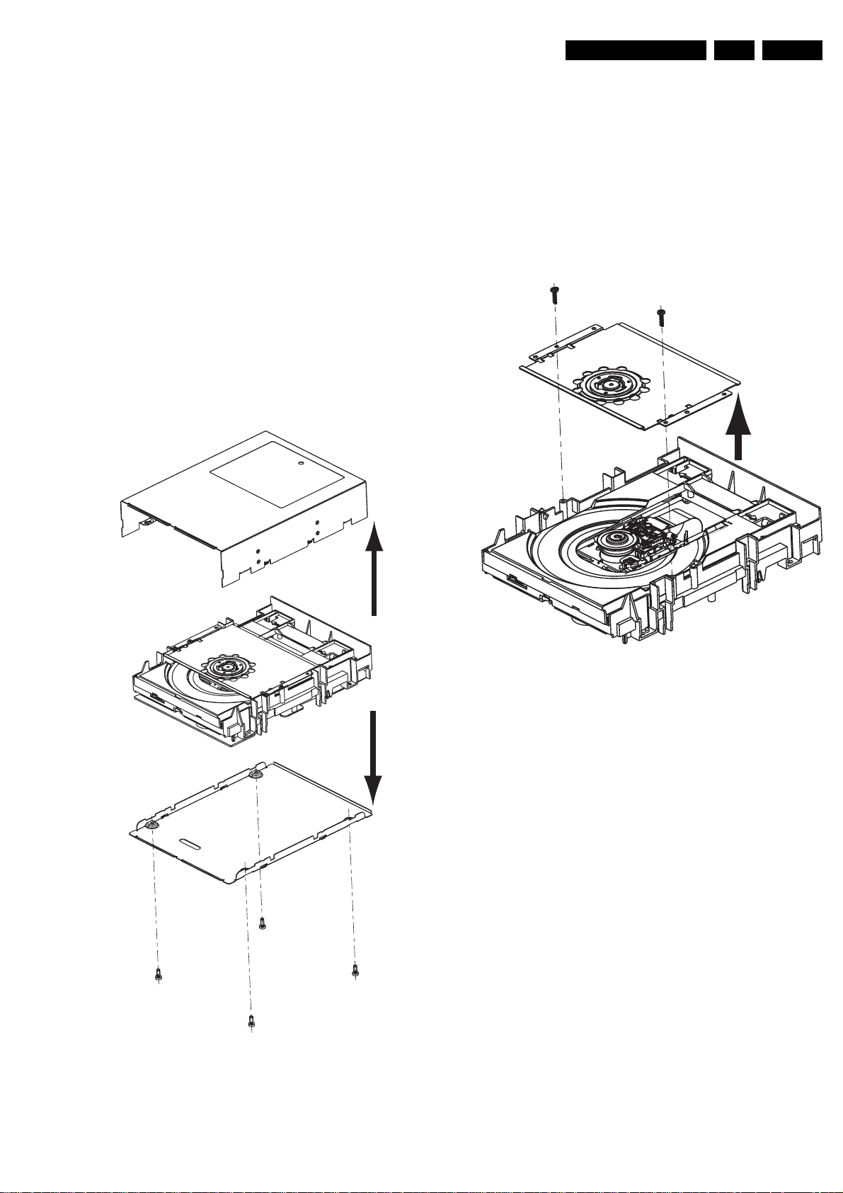
4.3 Cab inet and Clamper Bridge
– Remove the encasing by releasing the four screws [1], see
figure 4-1
– Make sure that you do not lose the 5 heat paths (gray
rubber pieces that conduct the heat from the ICs to the
case)!
– Remove the clamper bridge assy, by releasing the two
screws [1], see figure 4-2
1
1
2
1
2
Figure 4-2 Remove Clamper Bridge
2
1
1
1
Figure 4-1 Basic Engine dismantling (part1)
Page 6
EN 6 VAD 80314.
4.4 Tray
– Remove encasing as as described in 4.3
– Disengage the two holders that fix the tray [1], see figure 4-
3, and pull out the tray [2]
1
1
Mechanical Instructions
2
1
1
2
Figure 4-3 Remove Tray
4.5 Printed Board
Note: After Exchanging the PWB (or the DVD-M) the complete
drive has to be adjusted! Refer to chapter 8 for adjustment
instructions!
– Remove encasing and clamper bridge as described in 4.3
– Disconnect the four flex foils from the PWB connectors
– Remove the 2 screws that hold the PWB, see figure 4-4
– At assembly make sure that the 5 heat paths (gray rubber
pieces) are placed on the ICs!
Figure 4-4 Remove PWB
4.6 DVD-M
Caution: Never try to align or repair the DVD-Module itself!
Only the factory can do this properly. Service engineers are
only allowed to exchange the sledge motor assy.
After Exchanging the DVD-M (or the PWB) the complete drive
has to be adjusted! Refer to chapter 8 for adjustment
instructions!
– Remove encasing, clamper bridge and PWB as described
in 4-3 and 4-5
– Remove the four screws [1], see figure 4-5.
– Now you can remove the DVDM
2
1
1
Figure 4-5 Remove DVDM
1
1
Page 7
4.7 Sledge Motor Assembly
Caution: Never try to align or repair the DVD-Module itself!
Only the factory can do this properly. Service engineers are
only allowed to exchange the sledge motor assy.
– Place the DVD-Module, with the laser facing downwards
on a soft surface.
– Remove the three screws that hold the sledge-motor assy
and lift the assy upwards. You can replace it now.
Mechanical Instructions
EN 7VAD 8031 4.
Figure 4-6 Remove Sledge Motor Assy
4.8 Re-assembly
To re-assemble the module, do all processes in reverse order.
Take care of the following:
• Sledge-motor assy: Mesh the teeth of the sledge motor
and sledge rack properly, during mounting of the sledge
motor assy.
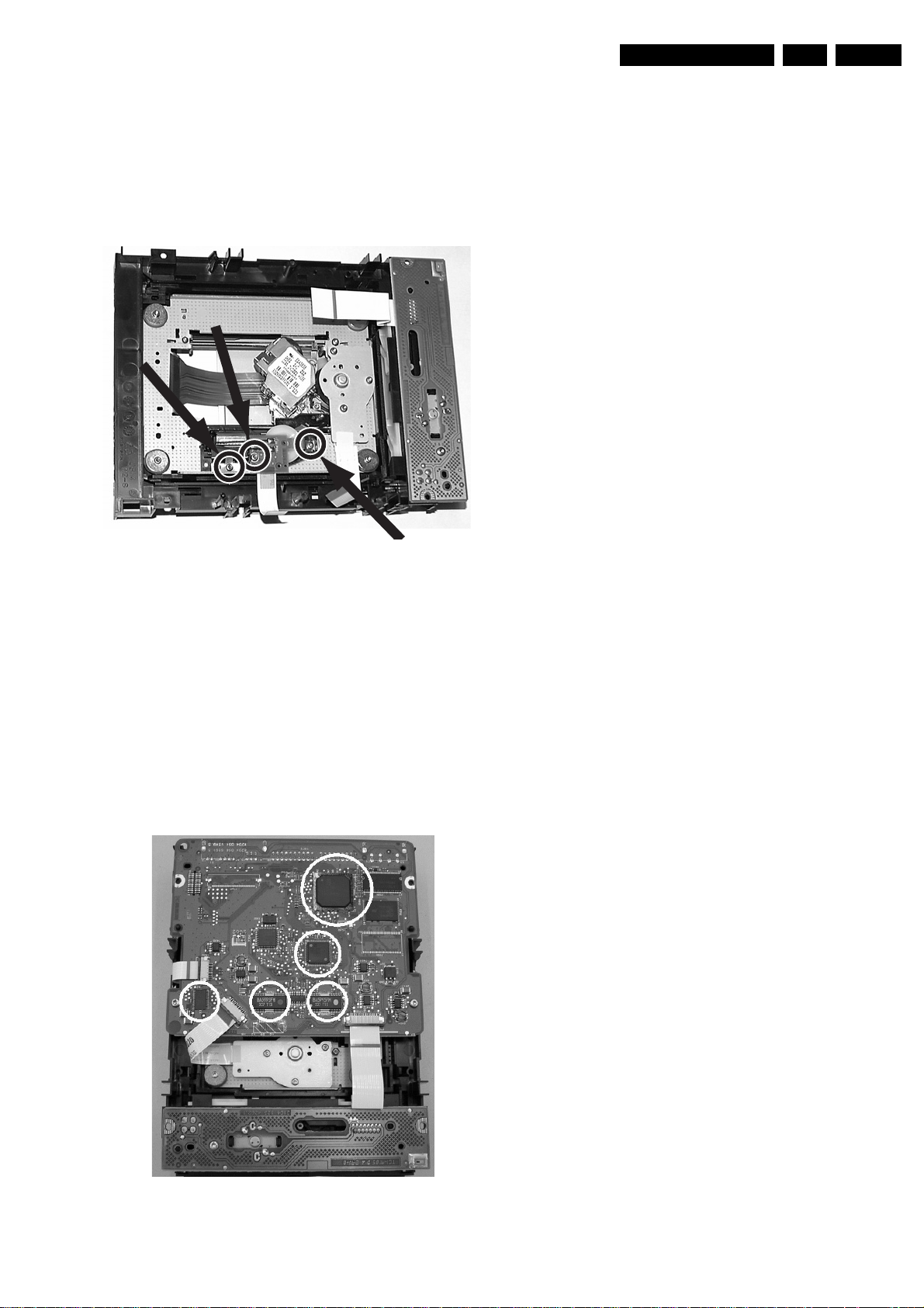
• Heat Paths: Put the 5 heat paths (gray rubber pieces) back
to their position on the ICs, see figure 4-7.
• Complete module: Place all wires/cables in their original
positions
• Emergency opening slot: Be sure that the slot for the
emergency tray opener is covered by adhesive tape!
• Jumper selection: Jumper has to be in position "Master"!
Figure 4-7 Heat Paths
Page 8
EN 8 VAD 80315.
5. Diagnostic Software
Diagnostic Software
5.1 General
Please refer to the service manual of the recorder for a
description of the complete Diagnostics Software. In this
manual only drive specific error codes are explained.
5.2 Error Codes
With DSW command 910 (Digital Board Chrysalis) the set
software can retrieve an overview of all occurred engine errors.
5.2.1 Momentary Errors
Byte 0: latest error:
Overview of the BE error codes.
error
error meaning
code
0x00 no_error No error has occurred
0x01 illegal_command_error Command not allowed in this
state or unknown command
0x02 illegal_parameter_error Parameter(s) not valid for
0x03 command_timeout_error The maximum execution
0x04 sledge_home_error The sledge could not be
0x05 sledge_calibration_error An error occurred during cal-
0x06 sledge_unstable_error The sledge detected unsta-
0x07 speed_timeout_error Spindle motor could not
0x08 speed_window_error Measured spinning speed is
0x09 focus_timeout_error Focus could not be achieved
0x0A focus_retries_error The amount of focus retries
0x0B focus_agc_error The focus agc results are out
0x0C radial_timeout_error Servo didn’t get on track
0x0D radial_retries_error Servo didn’t get on track after
0x0E radial_agc_error The radial agc results are out
0x0F radial_init_error Unreliable signal scaling af-
0x10 hf_pll_error HF-decoder pll could not lock
this command
time for the command has
exceeded
moved home
ibration of the sledge
ble control
reach its target speed within
timeout
not within expected window
within the timeout
expired
of range
within the timeout
several retries
of range
ter the radial initialisation
to HF signal
0x11 wobble_pll_error Wobble pll could not lock to
wobble signal
0x12 subcode_timeout_error Subcode information could
not be read
0x13 subcode_notfound_error Requested subcode item
0x14 header_timeout_error Header information could not
0x15 adip_timeout_error Adip information could not be
0x16 adip_window_error Adip address was not within
0x17 adip_sync_error No adip sync was detected
0x18 atip_timeout_error Atip information could not be
0x19 atip_notfound_error Requested atip item could
0x1A atip_window_error Atip address was not within
0x1B atip_sync_error No atip sync was detected
0x1C tray_error Tray could not be closed or
0x1D seek_error T he requested seek couldn’t
0x1E no_hf_present_error Attempt to read from a blank
0x1F record_error An error occurred during the
0x20 illegal_stopaddress_error The requested stopaddress
0x21 no_disc_error No disc is detected
0x22 not_initialised_error The system is not initialised
0x23 illegal_medium_error BE detected an unsupported
0x24 cd_frequency_error Measured HF frequency is
0x25 dvd_frequency_error Measured HF frequency is
0x26 re-
served(non_existing_bca_
error)
0x27 reserved(bca_read_error) An error occurred during
0x28 selftest_error An error occurred during the
0x29 i2c_error The I2C interface does not
0x2A laser_pll_error Laser control pll did not lock
0x2B laser_forward_sense_errorForward sense value didn’t
0x2C jitter_optimisation_error An error occurred during op-
0x2D tilt_calibration_error An error occurred during cal-
0x2E reserved
could not be found
be read
read
expected window
read
not be found
expected window
opened within the timeout
be performed within the timeout
area
recording
with modify-stop-address is
not valid
(e.g. seek on unknown disctype)
medium during disc recognition
not within CD frequency
range
not within DVD frequency
range
Attempt to read non-existing
bca information
reading of bca information
self-test of the BE
operate
or lost lock on write clock
change with changing laser
power
timisation of the jitter
ibration of the tilt frame
Page 9

Diagnostic Software
EN 9VAD 8031 5.
0x2F frontend_offset_calib_errorThe offset in the frontend
0x30 reserved
0x31 wsg_calculation_error An error occurred in the cal-
0x32 buffer_overrun_error The buffer input stream over-
0x33 return_value_invalid_error The requested information is
0x34 illegal_recording_speed_e
rror
0x35 opc_media_parameter_errorThe media parameters (info
0x36 opc_record_power_error The final optimum power was
0x37 opc_start_power_low_errorOPC start power too low (op-
0x38 opc_start_power_high_errorOPC start power too high
0x39 opc_power_calculation_er
ror
0x3A opc_test_zone_full_error OPC can’t be performed be-
0x3B opc_bad_jitter_measurem
ent_error
0x3C opc_read_samples_error An error occurred during
0x3D ropc_alpha_overflow_error The determined value for the
0x3E ropc_alpha_ref_current_er
ror
0x3F ropc_alpha_gain_error The alpha measurement al-
0x40 beta_over_under_flow_errorDuring the walking OPC a
0x41 not_enough_calib_points_
error
0x42 not_enough_power_error The calculated power during
0x43 illegal_reading_speed_errorThe selected speed is not al-
0x44 servo_fatal_error The actuator dissipation be-
couldn’t be calibrated
culation of the write strategy
ran the buffer output stream
not available for this inquiry
The selected speed is not al-
lowed for a recording on this
medium
in ATIP/ADIP) are invalid or
not read
not reached
timum power is higher)
(optimum power is lower)
Error during OPC power cal-
culation (samples are wrong)
cause test zone is full
The jitter measurement dur-
ing OPC samples readback
failed
OPC readback sampling
optimum power is too high
The alpha measurement ref-
erence current is wrong (IAN)
pha gain is wrong
beta over-/under-flow was
detected
Not enough valid calibration
points available for re-calibration
re-calibration exceeds max
power
lowed for the requested command
came too high during a servo
recovery
This error is overwritten by the next player / inquiry command.
Page 10

EN 10 VAD 80315.
Diagnostic Software
Byte 1 - 9: cumulative errors of previous error occurences.
Format of the BE error bytes
Every individual error has its own bit in the 9-byte structure as
described in the drawing below:
byte 1
b7 b6 b5 b4 b3 b2 b1 b0
reserved
FOCUS
AGC
ERROR
FOCUS
RETRIES
ERROR
FOCUS
TIMEOUT
ERROR
RADIAL
AGC
ERROR
RADIAL
RETRIES
ERROR
RADIAL
TIMEOUT
ERROR
byte 2
TRAY
ERROR
reserved
JITTER
OPTIMIZATION
ERROR
SLEDGE
HOME
ERROR
SLEDGE
UNSTABLE
ERROR
SLEDGE
CALIBRATION
ERROR
TILT SENSOR
OFFSET
CALIBRATION
ERROR
byte 3
RECORD
ERROR
SEEK
ERROR
NO DISC
ERROR
NOT
INITIALISED
ERROR
ILLEGAL
STOPADDRESS
ERROR
ILLEGAL
PARAMETER
ERROR
ILLEGAL
COMMAND
ERROR
byte 4
SERVO
FATAL
ERROR
reserved reserved
HF PLL
ERROR
NO HF
PRESENT
ERROR
HEADER
TIMEOUT
ERROR
SUBCODE
NOTFOUND
ERROR
RADIAL
INIT
ERROR
TILT
CALIBRATION
ERROR
COMMAND
TIMEOUT
ERROR
SUBCODE
TIMEOUT
ERROR
byte5
WOBBLE PLL
ERROR
byte6
WSG
CALCULATION
ERROR
byte7
LASER
FORWARD
SENSE
ERROR
byte8
OPC
READ
SAMPLES
ERROR
byte9
ADIP
SYNC
ERROR
DVD
FREQUENCY
ERROR
NVRAM
CHECKSUM
UPDATE
ERROR
OPC
BAD JITTER
MEASUREMENT
ERROR
ADIP
WINDOW
ERROR
CD
FREQUENCY
ERROR
FRONTEND
OFFSET
CALIBRATION
ERROR
OPC
TEST ZONE
FULL
ERROR
ADIP
TIMEOUT
ERROR
ILLEGAL
RECORDING
SPEED
ERROR
LASER PLL
ERROR
OPC
POWER
CALCULATION
ERROR
ATIP
NOTFOUND
ERROR
SPEED
WINDOW
ERROR
ILLEGAL
READING
SPEED
ERROR
OPC
START
POWER HIGH
ERROR
ATIP
SYNC
ERROR
SPEED
TIMEOUT
ERROR
ILLEGAL
MEDIUM
ERROR
OPC
START
POWER LOW
ERROR
ATIP
WINDOW
ERROR
NON
EXISTING
BCA
ERROR
SELFTEST
ERROR
OPC
RECORD
POWER
ERROR
ATIP
TIMEOUT
ERROR
BCA
READ
ERROR
I2C
ERROR
OPC
MEDIA
PARAMETER
ERROR
RETURN
VALUE
INVALID
ERROR
BUFFER
OVERRUN
ERROR
BETA
OVER/UNDER
FLOW
ERROR
NOT ENOUGH
CALIB POINTS
ERROR
These errors are kept in memory until a power down of the
drive (e.g. when recorder goes to standby) or reset of the drive.
NOT ENOUGH
POWER
ERROR
ROPC
ALPHA
GAIN
ERROR
ROPC
ALPHA
REF CURRENT
ERROR
ROPC
ALPHA
OVERFLOW
ERROR
Page 11

5.2.2 Cumulative errors
These errors are stored in EEPROM and are thus non-volatile
showing the complete error history of the drive.
Byte 1 - 9: cumulative errors of previous player / inquiry error
occurences. These bytes are the same as the nine bytes (1-9)
of the Momentary errors
5.2.3 Software fatal assert
Gives row number and file name in the source code of the
firmware of the data path of the AV
Diagnostic Software
EN 11VAD 8031 5.
Page 12

EN 12 VAD 80315.
Diagnostic Software
Page 13
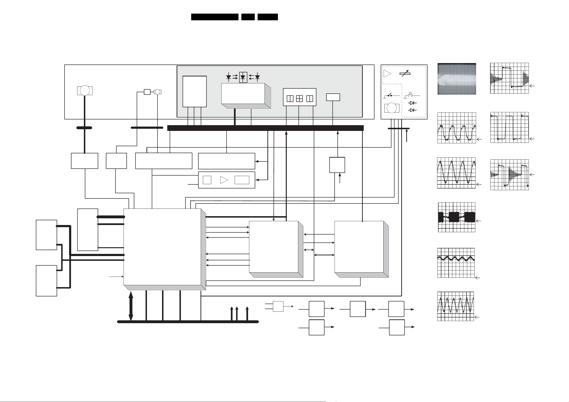
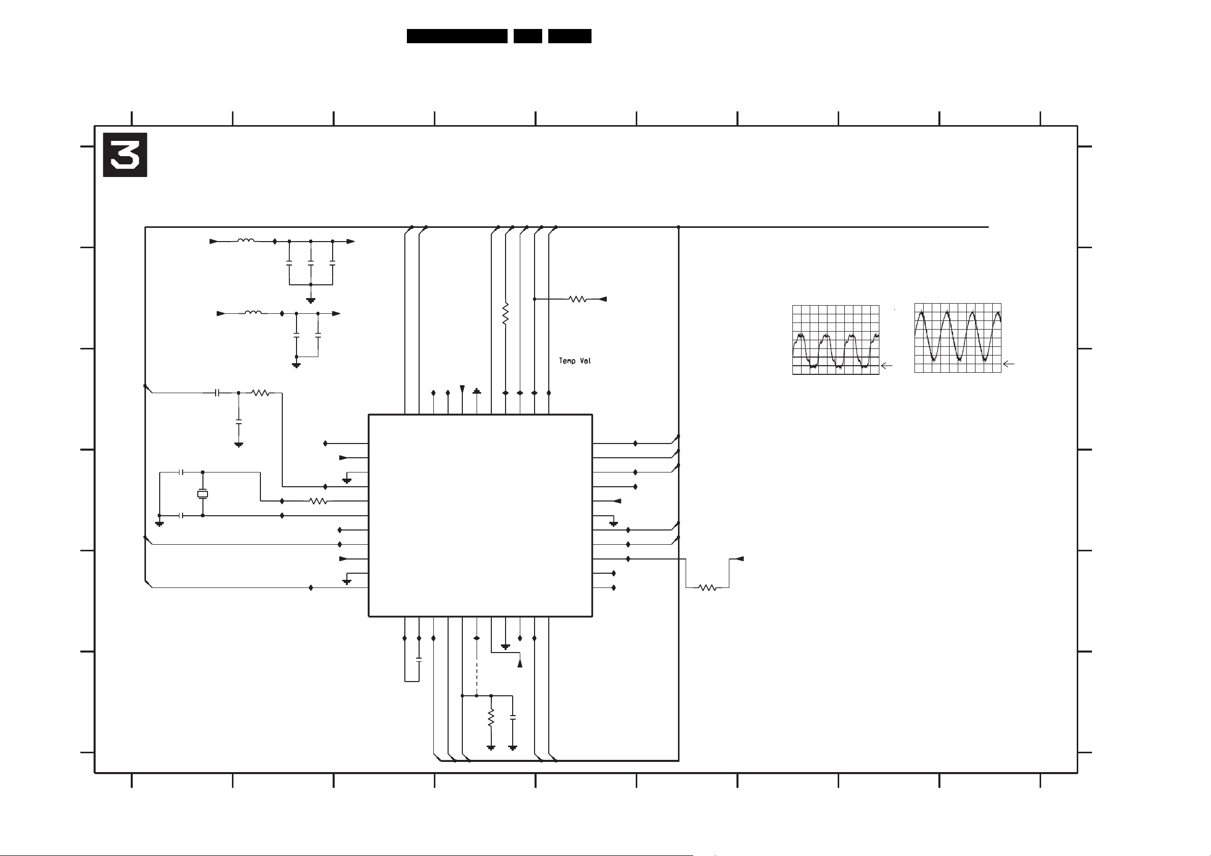
6. Block Diagram.
Block Diagram
Disc Motor
M
11P
1401
7402
Disc Motor Driver
option
SRAM
7503
TZA1015
7504
SDRAM
16MB
U,V,W coil
U+,UV+,VW+,WHall+ ,Hall-
MOTO1
MOTOR-ON
VMOTO10
T1
7400
XDD0..15
XDA0..11
DATA_MASK
DA0..15
AD0..19
PCS-p re_amp
SIN H
COSPH
REFSIN
REFCOS
7500
XWR
XRAS
SDCK
XCASL
XCASH
1400
LOADER
+SI N , - SIN
+COS, -COS
7409
ROHM
Block Diagram.
PCS
Sled g e
M
9P
SL-
SL+
Servo D ri v e r
BA5995FM
SL
FO+
FORA
TRAY-INOUT
TRAY-ONOFF
DRIVER-ON
CENTAURUS
FOC+
FOC-
Actuator
RADIAL
FOCUS
TILT
1V65
7408
7405
DC
level
laser 650nm
RAD
Servo D r iv er
BA5995FM
SID A , SILD, SICL
RFREF
RFN3 ,RFP3
A1,2
CALF
XDN
FTC
D1..4
PPNO
F S diode
E la ntec 6295
SCLK
SDI O
SEN
offset
gain
TRAYSW
EJECTKEY
DEBUG1,2,4,5
laser 780nm
EFM
R/ W
SERVO-M EA S
SERVO-COM M
FOC-
FOC+
13VAD 8031 6.
650nm PD
RAD
OPU66
PAEDIC
TZA 1045
CD-MO DE
VIA..H RF P ,R F N IIC
HIGH-GAIN
VIA..H
RFP
RFN
E FMDATAP
EFM _ D A TA
EFM CLKN
EFM CLKP
EFM _ RWN
7201
highpower
IIC
LASP
ALFA
EEpr o m
7104
PAEDIC
power
7300
4V6
1002 Tr a y Motor PWB Assy
option
for Data
Drive
Headphones
Tray Switch
Eject key
R F N3 / R F P3, IC 7201 P in 38/39
A:AC, 50mV/Div
50ns/Div
M
15P
5V
3V3
LED
1702
Tr a y Motor
OPU Flex 45p
1100
Iodel
IOthr
IAPC
WSB
SCLK
SDIO
SEN
RW-Del
Vdel
5V
VREF
Vthr
HIGH-GAIN
CD- M ODE
LACONICCHEETA H
TR+
TR-
IC7300 Pin 4
A: DC , 1 V /Div, 20ns/Div
IC7300 Pin 5
A: DC , 500mV/Div, 20ns/Div
1401 Pin 9/10/11
A: DC , 5 V /Div, 500us/Div
1400-2,3,4,6,7, 8
IC 7604 P in 4
A: DC , 1 V/Div, 1us/Div
IC 7606 P in 1
A: DC , 2 V/Div, 1us/Div
IC 7605 P in 7
A: DC , 2 V/Div, 1us/Div
FLASH
PROM
1600
PORN
HD0..15
IDE
HDASPN
CS0
CS1
HA0
HA1
HA2
HPDIAGN
HIRQ
HDACKN
IOR DY
HDRN
HRWN
HDRQ
RX1_MASTER
TX1
TX2
DEBUG11
AUDIOR
AUDIOL
IEC958
5V
From/To DVD Recorder application
GND
12V
IR Q N,OSTR,EFM_RW N
1V8
3V3
RESET
PORN
7502
7603
5V
12V
3v3 1V8
5V25
5V
7606
7604
TOSTOCEN
A: DC , 500mV/Div, 2ms/Div
IC7504 Pin 38
7605
5V
-5V
1V65
TR 15001_002
100903
A: DC , 500mV /Div, 5ns/Div
Page 14
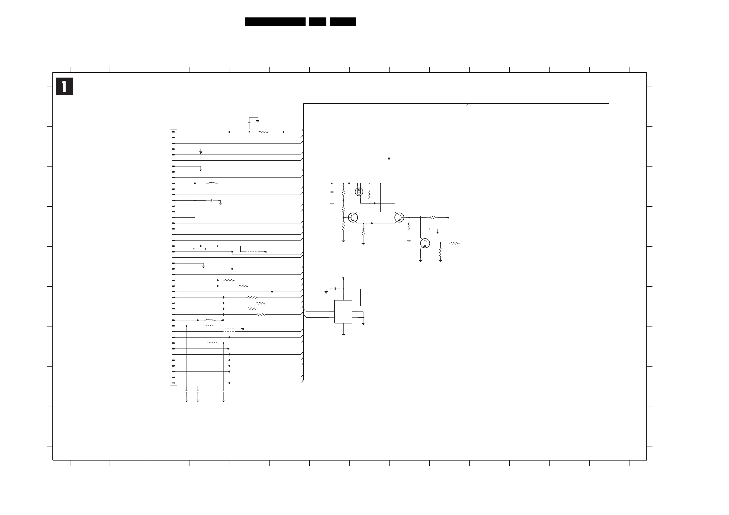
Electrical Diagrams and Print-Layouts
7. Electrical Diagrams and Print-Layouts
Servo Board: OPU Interface
14VAD 8031 7.
1 2 3 4 5 6 7 8 9 10 11 12 13 14
1100 A3
2100 C4
2101 H4
A
2102 E4
2103 A5
2104 H3
2105 H4
2106 D9
TO CHEETAH_QD/DRIVERS/CENTAURUS-DRAM-FLASHROM/DEBUG-AND-FLASH
{SERVO-MEAS,VREF,Vdel,Vthr,ENA,RW-Del,HIGH-GAIN,CD-MODE,VIG,VIE,VIA,VID,RFP,RFN,VIB,VIC,VIH,VIF,SERVO-COMM,FOC-,FOC+,RAD,IOthr,EFM-DATAP,EFM-DATAN,EFM-CLKP,EFM-CLKN,EFM_RWN,SCLK,SDIO,SEN,BUSY,IoDel,WSB,SCL,SDA,HIGHPOWER}
A
2107 C7
B
C
D
E
F
G
H
2108 F7
2110 B7
3100 E5
3101 E4
3103 F5
3104 B5
3105 F5
3106 F5
3107 F5
3110 D10
3111 E10
3112 D9
3113 D10
3114 D8
3115 C8
3116 C7
3117 D7
3118 D7
3119 B7
3120 A7
4100 D7
4105 G4
4106 C8
4107 C8
4108 C8
4109 D5
4110 E5
4111 F4
4112 G4
5101 C4
5102 F4
5103 F4
5104 G4
7101 D9
7102 D9
7103 D8
7104 C8
7105 F7
7107 B8
I100 B4
I101 B6
I102 F6
I103 G4
I104 G4
I106 G4
I107 H4
I108 G5
I110 E4
I111 E4
I115 D4
I116 F4
I117 F4
I118 F4
I119 F4
I120 C4
I121 C8
1100
AF3
45
44
43
B
C
D
E
F
G
42
41
40
39
38
37
I120
36
35
34
33
32
31
30
29
28
27
26
25
24
23
22
21
20
19
18
17
16
15
14
13
12
11
10
9
8
7
6
5
4
3
2
1
I115
100n
I128
I129
5102
5103
2102
5101
2100
100n
5104
I100
I130
I131
I110
3101
I111
82R
I116
I117
I118
I119
D3V3
4112
4105
I104
I103
I106
L100
I107
I108
+12V
10u
3100
100p
2103
3104
100R
4110
82R
3103
1K1K3105
3106
1K
3107
1K
+5V25
+5V25
I102
I101
HIGH-GAIN
EFM-DATAP
EFM-DATAN
SERVO-MEAS
SERVO-COMM
RW-Del
CD-MODE
VREF
SDIO
SCLK
EFM_RWN
EFM-CLKN
EFM-CLKP
WSB
IOthr
IoDel
FOC-
FOC+
RAD
VIG
VIE
VID
VIA
RFN
RFP
VIC
VIB
VIH
VIF
SCL
SDA
Vdel
Vthr
SEN
SDA
SCL
2107
2108
100n
LM75ADP
3
1
2
I121
1K5
22u
3116
7104
BSH205
7103
BC847B
7
6
5
3114
3115
820R
I122
3117
220R
I124
1K
3118
D3V3
8
7105
+VS
A0
OS
SDA
A1
SCL
A2
GND
4
+5V25
4108
3K3
I123
3112
1K
7102
BC847B
I125
2106
100n
7101
BC847B
I126
3113
3V3
1K0
I127
10K
3111
HIGHPOWER
3110
10K
H
2101
2104
100n
2105
100n
220p
I122 C7
I123 C8
I124 D7
I125 D9
I126 D8
I
I
I127 D10
I128 F4
I129 F3
I130 E5
I131 E5
TR 15002_001
100903
I132 A8
I133 B7
L100 H4
1 2 3 4 5 6 7 8 9 10 11 12 13 14
Page 15
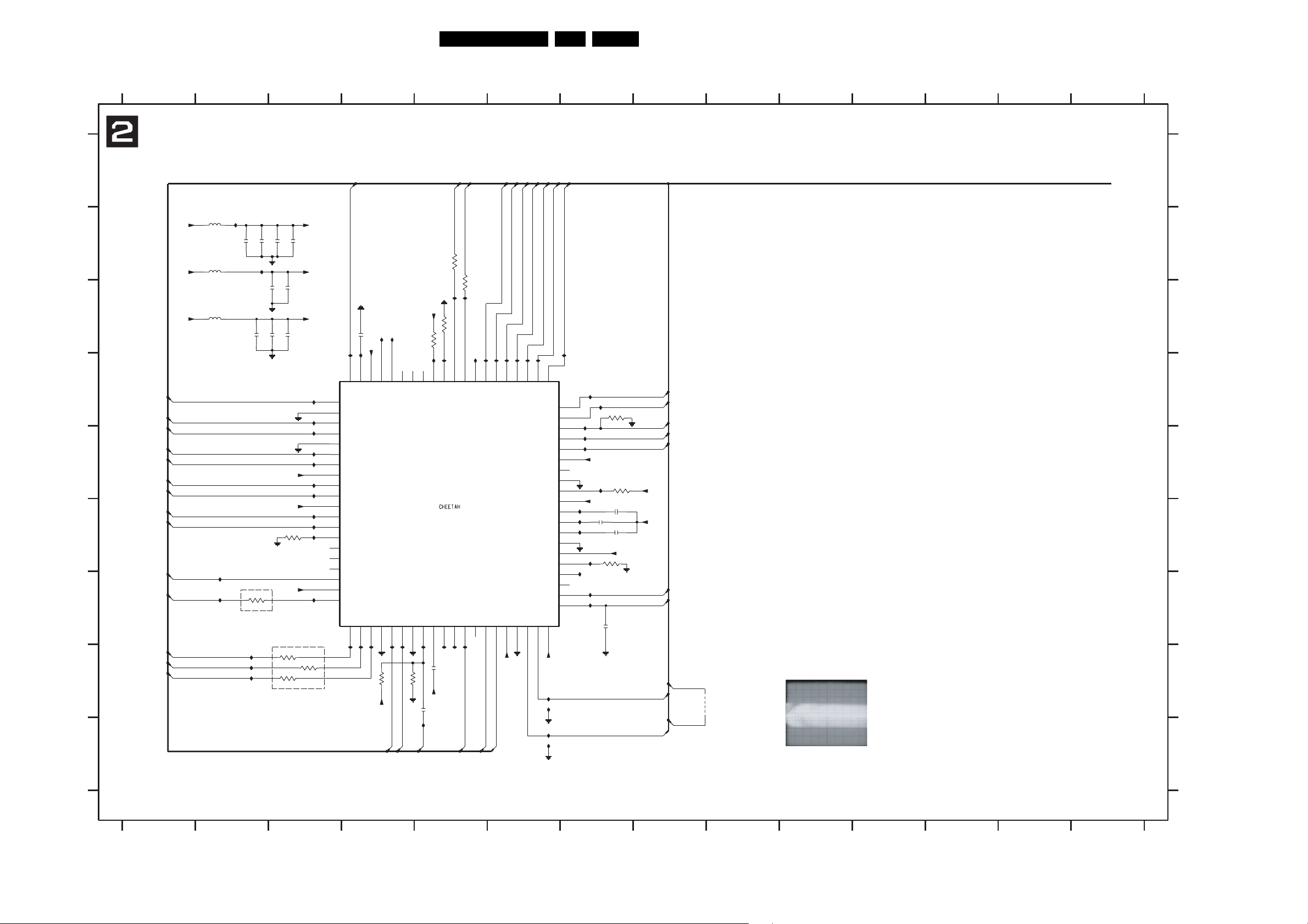
Servo Board: Cheetah
Electrical Diagrams and Print-Layouts
15VAD 8031 7.
1 2 3 4 5 6 7 8 9 10 11 12 13 14
A
5202
5204
5201
I201
2209
100n
5VA
B
-5V
C
-5V
2206
D
VIH
VIC
VIB
RFN
E
RFP
VID
VIA
VIE
VIG
F
TIMOUT
EFM-CLKN
G
EFM-CLKP
EFM-DATAN
H
EFM-DATAP
I253
I254
CLOSE TO IC7500
3209
1K8
I261
I262
I263
I
{TIMOUT,RFP,RFN,VIA,VIB,VIC,VID,VIE,VIF,VIG,VIH,EFM-CLKP,EFM-CLKN,EFM-DATAP,EFM-DATAN,TS1,TS2,LASP,PPNO,RFP3,RFN3,RFREF,CALF,A1,A2,XDN,D1_TILTN,D2_TLN,D3_REN,D4_FEN,S1_MIRN,S2,MON1,MON2,SIDA,SICL,SILD,SDA,SCL,ALFA,FTC,VERSION0,VERSION1,RW-Del,R-W,GEN-INP0,GEN-INP1,EFMCLK-O,EFM_DATA_P_del,EFM_DATA_N_del,EFM-DATAP,EFM-DATAN,RWN,PORN,EFM_RWN}
A1
VIF
LASP
ALFA
A2
CALF
XDN
D2_TLN
D1_TILTN
D3_REN
TO OPU/EPLD-LADIC-CON/LACONIC_IC/CENTAURUS
+5Vd
2212
100n
100n
2211
100n
2210
3201
3205
I225
72
NC8
CFTC
29
2217
10n
I243
10K
3203
1%
47K
I209
71
TEST
TZA1039HL
30
I246
I245
47n
100R
3200
100R
I242I244
I203
D163D262D3
VDD1-3
GND1-4
VSS1-2
CCALF
GND1-3
VSS1-1
SERTST
RFREF
RFP
RFN
39
-5Va
61
MON2
MON1
CMPP
RREF
CA2
CA1
PPN
NC7
NC6
VSS2
I202
I216
I217
60
D4
59
S1
58
S2
57
56
55
54
53
52
51
I234
50
I237
49
I239
48
47
46
45
L201
44
43
42
41
40
I219
I221
I222
I236
I238
I241
+5Vd
I228
-5Va
2214
3214
27K
2213
2215
10n
10n
3208
10K
2223
27n
100n
3206
47K
-5Vd
D4_FEN
S1_MIRN
S2
MON2
MON1
-5Va
1%
-5Va
PPNO
RFREF
69
70
ALFA
LASP
TS131TS2
SILD
32
SROUT
NC5
33
A167A2
34
65
64
XDN
CALF
VDD2
SICL35SIDA
GND2
37
36
38
I204
I207
I205
I208
I206
L200
68
66
+5Vd
RFN3 / RFP3, IC7201 Pin 38/39
TIMOUT
RFN3
4201
RW-Del
RFP3
SILD
SIDA
SICL
I257
I258
I259
I260
I256
100n
2219
2207
-5Vd
100n
2220
100n
-5Va
100n
2222
100n
I215
I218
I220
I224
I226
+5Vd
I227
I229
+5Vd
I231
I233
I235
3207
10K
-5Vd
I240
CLOSE TO IC7500
3210
3211
1K8
3212
1K8
1K8
7201
-5Va
100n
2221
I223
I214
-5Va
I212
I265
78
79
80
VIF
VREF
VIH
GND1-1
VIC
VIB
GND1-2
RFNIN
RFPIN
VDD1-1
VID
VIA
VDD1-2
VIE
VIG
R|W
NC1
NC2
NC3
TIMOUT
VSSD
EFMCN
I252
EFMCP21EFMDN
22
I251
I250
VSS1-3
EFMDP
23
1
2
3
4
5
6
7
8
9
10
11
12
13
14
15
16
17
18
19
20
3217
77
WRF
GNDD
74MI73
75
76
LD
RRF
VDDL
SCL26SDA
NC4
I248
27
3213
FTC
28
I247
18K
24
25
I249
33K
-5Va
+5Vd
2218
I264
SDA
SCL
FTC
A:AC, 50mV/Div
50ns/Div
2204 B5
2205 B5
2206 C2
2207 C3
2209 B2
2210 B2
2211 B3
2212 B3
2213 F7
2214 F7
2215 F7
2217 H5
2218 H5
A
2219 C3
2220 C3
2221 C4
2222 C3
2223 G7
3200 C5
3201 B5
3202 C4
3203 C5
3204 C4
3205 C5
3206 E7
B
3207 F3
3208 F7
3209 G2
3210 H3
3211 H3
3212 H3
3213 H4
3214 D7
3215 D3
3216 D3
3217 H4
4200 H9
C
4201 H8
5201 C2
5202 B2
5204 B2
7201 D3
I201 B2
I202 D6
I203 D6
I204 D6
I205 D6
I206 D6
D
I207 D6
I208 D5
I209 D5
I212 D4
I214 C4
I215 D3
I216 D7
I217 D7
I218 D3
I219 D7
I220 E3
I221 E7
E
I222 E7
I223 C4
I224 E3
I225 D5
I226 E3
I227 E3
I228 E7
I229 E3
I231 F3
I233 F3
I234 F7
I235 F3
F
I236 F7
I237 F7
I238 G7
I239 F7
I240 G3
I241 G7
I242 C5
I243 C5
I244 H5
I245 H5
I246 H5
G
I247 H5
I248 H4
I249 H4
I250 H4
I251 H4
I252 H4
I253 G2
I254 G2
I256 B2
I257 H6
I258 H6
I259 I6
H
I260 I6
I261 H2
I262 H2
I263 H2
I264 I5
I265 D4
L200 D5
L201 F7
I
TR 15003_001
1 2 3 4 5 6 7 8 9 10 11 12 13 14
100903
Page 16
Servo Board: Laconic
A
B
OSC_IN
C
2303
D
ALFA
LASP
E
Electrical Diagrams and Print-Layouts
16VAD 8031 7.
1 2 3 4 5 6 7 8 9
TO OPU/EPLD/CENTAURUS
{WSB,RW-Del,R-W-Delayed,TIMOUT,OSC_IN,PORN,VERSION0,VERSION1,SCL,SDA,SCLK,SDIO,SEN,BUSY,ENA,HIGH-GAIN,CD-MODE,GEN-INP0,GEN-INP1,EFM-CLKP,EFM-CLKN,EFMDATA-3P,EFMDATA-3N,ALFA,LASP,Vdel,Vthr,VREF,IOthr,CD-MODE,HIGH-GAIN,IRQN,OSTR,RWN,SDA,SCL,IoDel}
5300
5301
15p
3303
150R
I303
I313
I308
I310
2301
2306
2302
100n
100n
I312
D3V3
A3V3 3V3A
2311
1n0
2312
15p
1302
16M93
2304
15p
CX-16F
2307
3315
33R
100n
2300
100n
3V3D
I320
3V3A
L308
L303
I311
100n
3V3D
1
2
3
4
5
6
7
8
9
10
11
AEZ
Vddd3
Vssd3
ClckOut
Osco
Osci
Test1d
Ameas
Vdda1
Vssa1
LasP
SCL
I316
SDA
44
SCL
VRefL
12
I317
L301
43
SDA
VRefH
13
L305
L307
42
Test2d
VDel
14
3V3D
41
Bank
VThr
15
39
40
Vssd2
Vddd2
7300
LACONIC
Vopuref16Vrefin
17
I314
RW-Del
38
RWn
Vdda2
18
PORN
3302
I304
37
Resetn
Vssa2
19
OSTR
1R
I305
36
OSTR
Test1a
20
L306
IRQN
I306
35
IRQn
IoDel
21
L310
WSB
L311
34
WSB
IoThr
22
3316
10K
SCLK
SDIO
SEN
Busy
Vddd1
Vssd1
HiLo
DvdCd
EnR1
EnR2
Test2a
3V3D
L309
L304
3V3D
I302
I315
I318
I300
I301
I319
SCLK
SDIO
SEN
HIGH-GAIN
CD-MODE
3V3D
3301
10K
33
32
31
30
29
28
27
26
25
24
23
IC7300 Pin 4
A: DC, 1 V/Div, 20ns/Div
IC7300 Pin 5
A: DC, 500mV/Div, 20ns/Div
A
B
C
D
E
1302 D1
2300 B2
2301 B2
2302 B2
2303 D1
2304 D1
2305 F3
2306 B2
2307 B2
2308 B5
2309 E6
2310 F4
2311 C1
2312 C2
3300 D2
3301 E6
3302 B4
3303 C2
3304 E5
3305 E5
3306 E6
3308 F4
3309 F4
3315 D2
3316 B5
4303 F4
5300 A2
5301 B2
7300 D4
I300 C5
I301 D5
I302 D5
I303 A2
I304 C4
I305 C4
I306 C4
I307 C1
I308 D2
I310 D2
I311 D3
I312 E2
I313 B2
I314 E4
I315 D5
I316 E3
I317 E3
I318 D5
I319 D5
I320 D2
L301 C3
L303 D3
L304 E5
L305 E3
L306 E4
L307 C4
L308 C3
L309 E5
L310 E4
L311 C5
F
22n
2305
Vdel
Vthr
4303
VREF
3309
1K8
3V3A
2310
100n
IoDel
IOthr
1 2 3 4 5 6 7 8 9
TR 15004_001
100903
F
Page 17

Electrical Diagrams and Print-Layouts
Servo Board: Drivers (Overview)
1 2 3 4 5 6 7 8 9 10 11 12 13 14 15 16 17 18 19 20 21
A
1400
I426
SL+
9
B
C
I440
SL-
8
7
COS-
6
SIN+
5
COS+
4
SIN-
3
I439
2
1
D
E
Left page
F
G
+5V
1R
3418
1401
1
H
I
HALL+
2
W-
3
W+
4
V+
5
HALL-
6
U+
7
V-
8
U-
9
UCOIL
10
VCOIL
11
WCOIL
J
K
1 2 3 4 5 6 7 8 9 10 11 12 13 14 15 16 17 18 19 20 21
3425
I420
I423
I425
I427
I428
I429
I431
I433
I435
I436
I437
2n2
2n2
2420
2419
2418
2412
I422
100n
82R
3412
82R
2n2
3421
BIAS_VH
2411
17VAD 8031 7.
I401 B6
1400 B2
I402 B6
{AUXPW,SERVO-COMM,SERVO-MEAS,TR+,TR-,HIGHPOWER,FO+,FO-,SL,RA,DRIVER-ON,FOC-,FOC+,RAD,TRAY-SW,TRAY-INOUT,TRAY-ONOFF,VFOO-,VFOO+,VRAOO,SL-,SL+,VSLOO,REFCOS,COSPHI,REFSIN,SINPHI,TOSTOCEN,TRAYSW,MOTOR-ON,T1,VMOTO1O,MOTO1}
D3V3
10K
I407
3403
D3V3
3400 3401
10K
100n
2403
1.6V
5
COS-
1.6V
6
COS+
I409
I410
3408
10K
1.6V
1.6V
I432
19.4V
10n
2414
2415
11.4V
I430
22n
0.1V
I434
7402
SZA1015
6FG
29 WP
28 VN
27 VP
25 UP
I415
2
I417
32 COSC
100p
I418
3 ROSC
47K
2.1V
20
17
15
1
12
CAPY
BOOSTER
WN30
UN26
BIAS
GND
VSSA
0.5V
10CP1
11CP2
HALL AMPLIFIERS
OSC
REGENERATOR
HEATSINK
33
4 REMF
I421
I419
12K
3422
3420
14W
SWITCHES
PWM
EMF
LIMITER
ADC
5 RLIM
0.9V
20K
21U
19V
POWER
SHUTDOWN
COMMUTATION
START
VDD
IC1
IC2
CURRENT
NC
7EC
8 ECR
3493
100n
2413
VDDM
THERMAL
470R
3
SIN+
2
SIN-
I414
+12V
5400
13
I438
16
22
23
24
9
31
18
3494
470R
3406
1K
10K
100n
2400
+5V
2405
100n
8
LM358D
4
3407
I411
3409
10K
2409
100n
+5V
8
LM358D
4
3410
56K
10u
2443
22u
2442
22u
100n
2417
I489
6401
BZX384-C5V1
D3V3
56K
2445
7400-B
7400-A
I406
TRAY-SW
2407
100n
I402I400 I401
I408
7
0.7V
I413
1
1.4V
D3V3
10K
3423
I424
+5V
3411
I416
3495
3496
1K2
3497
100n
3498
1K2
3499
I484
4402
1K
3487
1K
3488
4K7
MOTOR-ON
1K2
1K2
1K2
VMOTO1O
2444
TRAYSW
REFCOS
COSPHI
REFSIN
SINPHI
+12V
MOTO1
4u7
SL+
SL-
T1
TOSTOCEN
DRIVER-ON
FO-
VFOO-
FO+
VFOO+
SL
VSLOO
TRAY-INOUT
TRAY-ONOFF
I403
3405
10K
S1V65
S1V65
Remark: DC voltages are measured in DVD+RW playback
+5V
2421
4n7
3404
10K
2406
82n
I455
3474
12K
3477
12K
2401
1.6V
100n
3
8
I405
2
1.6V
3473
I457
4427
I465
4419
4422
3481
1R
I404
1
LM358D
4
7401-A
10K
I459
I467
I470
I473
I475
S1V65
3492
I441
1.6V
3446
1
1K2
LM324D
7405-A
+12Va
7405-B
LM324D
3461
7
1K2
1.6V
5405
+12V
7409
BA5995FM
STBY1
20
OPIN3-
23
OPIN3+
24
OPIN4-
26
OPIN4+
27
OPIN1-
3
OPIN1+
2
I485
3479
MUTE
6
10K
IN2
5
BIASIN
1
STBY2
7
10K
3485
1K0
3440
1K2
11
4
4
11
3464
1K2
I452
STBY
CH1/3/4
+
+
+
MUTE
CH1
STBY
CH2
S1V65
FOC+
I442
2.3V
3444
2
6K8
I444
3
2.3V
2.3V
5
I447
6
2.3V
I461I458
10u
2431
VCC19VCC2
+
+
+
+
I451
3447
6K8
3452
S1V65
1K2
3454
1K2
3457
6K8
3462
6K8
+12Va
2430
100n
I477
I478
2434
2n2
I480
I481
2435
2n2
28
10 19
VCC3
PREVCC
OPOUT3
-
VO3-
+
LEVEL
SHIFT
LEVEL
SHIFT
LEVEL
SHIFT
LEVEL
SHIFT
21
VO3+
+
OPOUT4
-
VO4-
+
VO4+
+
OPOUT1
-
VO1-
+
VO1+
+
-
-
VO2-
+
VO2+
+
-
GND18GND2
MT129MT2
30
4403 4400
S1V65
4405
SERVO-MEAS
RAD
I446
4406 4407
22
18
17
25
I464
16
15
4
I469
13
I471
14
2438
100n
3482
I472
11
12
1R
I474
2440
100n
S1V65
FOC-
SERVO-MEAS
DRIVER-ON
VRAOO
RA
S1V65
SL-
SL+
TR+
TR-
AUXPW
+12Va
2441
I486
3480
10K
3483
10K
3484
10K
100n
7405-D
12
4
LM324D
2.7V
I488
14
1.6V
13
11
2.7V
3486
10K
4404
+12V
20
I460
3472
12K
+5V
I487
23
4415
24
I462
26
27
S1V65
I482
3475
3
10K
2
I483
3476
6
10K
5
1
S1V65
7
5406
7408
BA5995FM
STBY1
OPIN3OPIN3+
OPIN4OPIN4+
OPIN1OPIN1+
MUTE
IN2
BIASIN
STBY2
4413
220R
3445
1K2
3450
6K8
3453
6K8
I453
STBY
CH1/3/4
+
+
+
MUTE
CH1
STBY
CH2
I443
+12Va
2.3V
10
4
2.3V
9
11
3460
1K2
I448
16V
10u
2433
100n
2432
10 19
VCC19VCC2
VCC3
-
LEVEL
+
SHIFT
-
LEVEL
+
SHIFT
-
LEVEL
+
SHIFT
-
LEVEL
+
SHIFT
GND18GND2
21
TO CENTAURUS/DEBUG-AND-FLASH
OPU /CENTAURUS/POWER-CONN-AUDIO/DEBUG CONN
7405-C
LM324D
I445
3451
8
1K2
1.6V
I476
28
PREVCC
+
+
-
+
+
-
+
+
-
+
+
-
MT129MT2
OPOUT3
VO3-
VO3+
OPOUT4
VO4-
VO4+
OPOUT1
VO1-
VO1+
VO2-
VO2+
30
2n2
2436
22
I479
18
I463
17
25
16
I468
4416
15
4
13
14
11
12
3489
27R
3491
I456
27R
3471
27R
3490
27R
Right page
1401 Pin 9/10/11
A: DC, 5 V/Div, 500us/Div
SERVO-COMM
1400-2,3,4,6,7,8
A: DC, 500mV/Div, 2ms/Div
TR 15005_001
100903
1401 H2
I403 B8
2400 C6
I404 B10
2401 A9
I405 B9
2403 C5
A
B
C
D
E
F
G
H
I
J
K
2405 C6
2406 B9
2407 A7
2409 E6
2411 J4
2412 H3
2413 K5
2414 G5
2415 H4
2416 I6
2417 I6
2418 J2
2419 J3
2420 J2
2421 A9
2430 E11
2431 E10
2432 E16
2433 E16
2434 F11
2435 F11
2436 F18
2438 I12
2440 J12
2441 J14
2442 I6
2443 H6
2444 K7
3400 B6
3401 B6
3403 A6
3404 B9
3405 B8
3406 A6
3407 D6
3408 E6
3409 E6
3410 F6
3411 I7
3412 I3
3418 H3
3420 K5
3421 J4
3422 K5
3423 G7
3425 H3
3440 C10
3444 C11
3445 C16
3446 C10
3447 C11
3450 C16
3451 C17
3452 C11
3453 C16
3454 D11
3457 D11
3460 D16
3461 D10
3462 D11
3464 D10
3471 F19
3472 G14
3473 G9
3474 H9
3475 H15
3476 H15
3477 H9
3478 I9
3479 I9
3480 J13
3481 I9
3482 I13
3483 J13
3484 K13
3485 J10
3486 K14
3487 D7
3488 F7
3489 F19
3490 G19
3491 F19
3492 B10
3493 K5
3494 K6
4400 B12
4402 K7
4403 C12
4404 C15
4405 C15
4406 D12
4407 D13
4410 D13
4411 D13
4413 D16
4415 G15
4416 G18
4417 G19
4419 H9
4422 I9
4427 H9
5400 H6
5405 E10
5406 E15
7400-A F6
7400-B D6
7401-A B9
7402 H4
7405-A C10
7405-B D10
7405-C C16
7405-D J14
7408 F15
7409 G10
I400 B6
I406 A7
I407 A6
I408 C7
I409 D6
I410 E6
I411 E6
I413 F7
I414 F6
I415 I4
I416 I7
I417 I4
I418 J4
I419 K5
I420 H2
I421 K5
I422 H3
I423 H2
I424 G7
I425 H2
I426 B3
I427 H2
I428 I2
I429 I2
I430 H5
I431 I2
I432 G5
I433 I2
I434 H4
I435 I2
I436 I2
I437 I2
I438 H6
I439 C2
I440 B3
I441 C10
I442 C11
I443 C16
I444 C11
I445 C17
I446 D12
I447 D11
I448 D16
I451 C11
I452 E10
I453 E16
I455 G9
I456 F18
I457 G9
I458 E10
I459 G9
I460 F14
I461 E11
I462 G15
I463 G17
I464 H12
I465 H9
I467 H9
I468 G17
I469 I12
I470 I9
I471 I12
I472 I12
I473 J9
I474 J12
I475 J9
I476 E18
I477 F11
I478 F12
I479 F18
I480 F11
I481 F12
I482 H15
I483 H15
I484 K7
I485 I10
I486 J13
I487 K14
I488 K13
Page 18

Electrical Diagrams and Print-Layouts
18VAD 8031 7.
Servo Board: Drivers (Left page)
1 2 3 4 5 6 7 8 9 10 11
D3V3
10K
A
1400
B
C
I426
SL+
9
I440
SL-
8
7
COS-
6
SIN+
5
COS+
4
SIN-
3
I439
2
1
2403
100n
Left page
D
1401 Pin 9/10/11
E
F
A: DC, 5 V/Div, 500us/Div
1400-2,3,4,6,7,8
1.6V
1.6V
A: DC, 500mV/Div, 2ms/Div
3403
D3V3
1.6V
1.6V
I407
3400 3401
10K
COS-
COS+
I409
I410
3408
10K
SIN+
SIN-
I414
100n
2400
+5V
5
8
6
4
I411
2409
100n
+5V
3
8
2
4
G
+5V
1R
3418
1401
H
I
1
2
3
4
5
6
7
8
9
10
11
J
HALL+
WW+
V+
HALLU+
VUUCOIL
VCOIL
WCOIL
I420
I423
I425
I427
I428
I429
I431
I433
I435
I436
I437
2418
3425
82R
2n2
2n2
2n2
2420
2419
I422
2412
100n
3412
82R
2411
3421
BIAS_VH
100p
47K
I415
I417
I418
2.1V
K
19.4V
2415
22n
7402
SZA1015
6FG
29 WP
28 VN
27 VP
25 UP
2
32 COSC
3 ROSC
20
17
15
1
I432
11.4V
I434
12
CAPY
BOOSTER
WN30
UN26
BIAS
GND
VSSA
0.5V
10n
2414
I430
0.1V
14W
10CP1
11CP2
HALL AMPLIFIERS
OSC
REGENERATOR
HEATSINK
33
4 REMF
5 RLIM
I421
I419
0.9V
12K
3422
3420
SWITCHES
PWM
EMF
ADC
20K
21U
19V
POWER
VDDM
THERMAL
SHUTDOWN
COMMUTATION
START
VDD
IC1
LIMITER
IC2
CURRENT
NC
7EC
8 ECR
3493
100n
2413
470R
13
16
22
23
24
9
31
18
3494
470R
+12V
10u
5400
I438
22u
22u
100n
I489
6401
BZX384-C5V1
D3V3
3406
1K
10K
2405
100n
LM358D
3407
56K
3409
10K
LM358D
3410
56K
2443
2442
2417
2445
I402I400 I401
7400-B
7400-A
7
1
1.4V
100n
100n
0.7V
I406
2407
I408
I413
D3V3
3423
I424
4402
3411
I416
3496
1K2
3498
1K2
3487
3488
10K
+5V
4K7
3495
1K2
3497
1K2
3499
1K2
I484
TRAY-SW
TRAYSW
SL+
REFCOS
COSPHI
1K
REFSIN
SINPHI
1K
MOTOR-ON
+12V
VMOTO1O
MOTO1
4u7
2444
SL-
T1
TOSTOCEN
DRIVER-ON
FO-
VFOO-
FO+
VFOO+
SL
VSLOO
TRAY-INOUT
TRAY-ONOFF
I457
I465
I405
1.6V
1.6V
4427
4419
4422
3481
1R
+5V
2401
100n
3
8
2
LM358D
4
7401-A
10K
3473
I459
I467
I470
I473
S1V65
I475
2421
4n7
I403
3405
10K
S1V65
S1V65
3404
10K
2406
82n
I455
3474
12K
3477
12K
Remark: DC voltages are measured in DVD+RW playback
3479
10K
+12V
1
3446
3461
1K2
1K2
3485
I485
I404
20
23
24
26
27
3
2
6
5
1
7
10K
3492
1.6V
1
LM324D
7405-A
+12Va
7405-B
LM324D
7
1.6V
5405
7409
BA5995FM
STBY1
OPIN3OPIN3+
OPIN4OPIN4+
OPIN1OPIN1+
MUTE
IN2
BIASIN
STBY2
1K0
3440
1K2
11
4
4
11
3464
1K2
I452
STBY
CH1/3/4
+
+
+
MUTE
CH1
STBY
CH2
2.3V
2.3V
2431
I442I441
2
I444
3
5
I447
6
I461I458
10u
S1V65
2.3V
3444
6K8
3447
6K8
3452
1K2
3454
1K2
3457
6K8
3462
6K8
2.3V
2430
10 19
VCC19VCC2
+
+
+
+
100n
VCC3
LEVEL
SHIFT
LEVEL
SHIFT
LEVEL
SHIFT
LEVEL
SHIFT
I480
821
I477
S1V65
+12Va
28
PREVCC
+
+
-
+
+
-
+
+
-
+
+
-
MT129MT2
I451
I478
2434
2n2
I481
2435
2n2
OPOUT3
VO3-
VO3+
OPOUT4
VO4-
VO4+
OPOUT1
VO1-
VO1+
VO2-
VO2+
30
TR 15005a_001
22
18
17
25
16
15
4
13
14tr
11
12
160903
1 2 3 4 5 6 7 8 9 10 11
Page 19

Electrical Diagrams and Print-Layouts
Servo Board: Drivers (Right page)
12 13 14 15 16 17 18 19 20 21
FOC+
4403 4400
I486
2.7V
I488
FOC-
SL-
SL+
TR+
TR-
12
13
2.7V
RAD
SERVO-MEAS
DRIVER-ON
VRAOO
RA
S1V65
AUXPW
+12Va
4
11
3486
10K
2441
100n
7405-D
LM324D
1.6V
POUT3
VO3-
VO3+
POUT4
VO4-
VO4+
POUT1
VO1-
VO1+
VO2-
VO2+
SERVO-MEAS
I446
4406 4407
I478
I481
22
18
17
25
I464
16
15
4
I469
13
I471
14
11
12
I472
I474
2440
2438
100n
100n
3482
1R
S1V65
3480
10K
3483
10K
3484
10K
12 13 14 15 16 17 18 19 20 21
19VAD 8031 7.
{AUXPW,SERVO-COMM,SERVO-MEAS,TR+,TR-,HIGHPOWER,FO+,FO-,SL,RA,DRIVER-ON,FOC-,FOC+,RAD,TRAY-SW,TRAY-INOUT,TRAY-ONOFF,VFOO-,VFOO+,VRAOO,SL-,SL+,VSLOO,REFCOS,COSPHI,REFSIN,SINPHI,TOSTOCEN,TRAYSW,MOTOR-ON,T1,VMOTO1O,MOTO1}
TO CENTAURUS/DEBUG-AND-FLASH
OPU /CENTAURUS/POWER-CONN-AUDIO/DEBUG CONN
I443
5406
7408
BA5995FM
STBY1
OPIN3OPIN3+
OPIN4OPIN4+
OPIN1-
3
OPIN1+
2
6
MUTE
IN2
5
BIASIN
1
STBY2
7
4413
220R
3445
1K2
3450
6K8
3453
6K8
I453
STBY
CH1/3/4
+
+
+
MUTE
CH1
STBY
CH2
2433
2.3V
16V
10u
I448
2432
VCC19VCC2
+
+
+
+
2.3V
10
9
100n
10 19
+12Va
LEVEL
SHIFT
LEVEL
SHIFT
LEVEL
SHIFT
LEVEL
SHIFT
GND2
21
3460
1K2
VCC3
GND1
8
4
11
7405-C
LM324D
28
PREVCC
I445
8
1.6V
+
+
-
+
+
-
+
+
-
+
+
-
MT129MT2
30
OPOUT3
VO3-
VO3+
OPOUT4
VO4-
VO4+
OPOUT1
VO1-
VO1+
VO2-
VO2+
3451
1K2
I476
2n2
2436
I463
I468
I479
4416
Right page
22
18
17
25
16
15
4
13
14
11
12
I456
3489
27R
3491
27R
3471
27R
3490
27R
SERVO-COMM
TR 15005b_001
100903
S1V65
44054404
+12V
20
I462
3475
10K
3476
10K
23
24
26
27
I482
I483
I460
4415
3472
12K
S1V65
+5V
S1V65
I487
14
1400 B2
1401 H2
2400 C6
2401 A9
2403 C5
A
2405 C6
2406 B9
2407 A7
2409 E6
2411 J4
2412 H3
2413 K5
2414 G5
2415 H4
2416 I6
B
2417 I6
2418 J2
2419 J3
2420 J2
2421 A9
2430 E11
2431 E10
2432 E16
2433 E16
2434 F11
2435 F11
2436 F18
C
2438 I12
2440 J12
2441 J14
2442 I6
2443 H6
2444 K7
3400 B6
3401 B6
3403 A6
3404 B9
3405 B8
3406 A6
D
3407 D6
3408 E6
3409 E6
3410 F6
3411 I7
3412 I3
3418 H3
3420 K5
3421 J4
3422 K5
3423 G7
E
3425 H3
3440 C10
3444 C11
3445 C16
3446 C10
3447 C11
3450 C16
3451 C17
3452 C11
3453 C16
3454 D11
3457 D11
F
3460 D16
3461 D10
3462 D11
3464 D10
3471 F19
3472 G14
3473 G9
3474 H9
3475 H15
3476 H15
3477 H9
3478 I9
G
3479 I9
3480 J13
3481 I9
3482 I13
3483 J13
3484 K13
3485 J10
3486 K14
3487 D7
3488 F7
3489 F19
H
3490 G19
3491 F19
3492 B10
3493 K5
3494 K6
4400 B12
4402 K7
4403 C12
4404 C15
4405 C15
4406 D12
4407 D13
I
4410 D13
4411 D13
4413 D16
4415 G15
4416 G18
4417 G19
4419 H9
4422 I9
4427 H9
5400 H6
5405 E10
5406 E15
J
7400-A F6
7400-B D6
7401-A B9
7402 H4
7405-A C10
7405-B D10
7405-C C16
7405-D J14
7408 F15
7409 G10
K
I400 B6
I401 B6
I402 B6
I403 B8
I404 B10
I405 B9
I406 A7
I407 A6
I408 C7
I409 D6
I410 E6
I411 E6
I413 F7
I414 F6
I415 I4
I416 I7
I417 I4
I418 J4
I419 K5
I420 H2
I421 K5
I422 H3
I423 H2
I424 G7
I425 H2
I426 B3
I427 H2
I428 I2
I429 I2
I430 H5
I431 I2
I432 G5
I433 I2
I434 H4
I435 I2
I436 I2
I437 I2
I438 H6
I439 C2
I440 B3
I441 C10
I442 C11
I443 C16
I444 C11
I445 C17
I446 D12
I447 D11
I448 D16
I451 C11
I452 E10
I453 E16
I455 G9
I456 F18
I457 G9
I458 E10
I459 G9
I460 F14
I461 E11
I462 G15
I463 G17
I464 H12
I465 H9
I467 H9
I468 G17
I469 I12
I470 I9
I471 I12
I472 I12
I473 J9
I474 J12
I475 J9
I476 E18
I477 F11
I478 F12
I479 F18
I480 F11
I481 F12
I482 H15
I483 H15
I484 K7
I485 I10
I486 J13
I487 K14
I488 K13
Page 20

Electrical Diagrams and Print-Layouts
Servo Board: Centaurus Part 1 (Overview)
20VAD 8031 7.
1 2 3 4 5 6 7 8 9 10 11 12 13 14 15 16 17 18 19 20 21
{AUXPW,TOSTOCEN,MRN,HIGHPOWER,RX2,OSC_IN,PORN,FO-,REFCOS,REFSIN,FO+,SL,RA,FTC,S1_MIRN,D1_TILTN,D2_TLN,D3_REN,D4_FEN,OSTR,CALF,A2,A1,XDN,COSPHI,SINPHI,EFM-DATAN,EFM-DATAP,EFM-CLKN,EFM-CLKP,PPNO,RFREF,RFP3,RFN3,T1,MOTO1,AUDIOL,AUDIOR,HRESET,HDASPN,CS1,CS0,HA2,HA0,HA1,HPDIAGN,HIRQ,HDACKN,IORDY,HRDN,HRWN,HDRQ,SDA,SCL,SILD,SICL,SIDA,RX2,TX2,TX1,RX1_MASTER,EJECTKEY,DRIVER-ON,MOTOR-ON,IRQN,TRAY-SW,TRAY-INOUT,TRAY-ONOFF,VRIN,IEC958,EFM_RWN}
JTAG_TCK
N8
VDD3P3
JTAG_TMS
JTAG_TDO_CENT
F5
E4
VSS3P2
VDD3P2
PORN
JTAG_TDI_CENT
N6
N5
A5
TRST
VSS3P1
VDD3P1
A4
TCK
XDD0
H16
XDD(0)
A2
A3
TMS
TDO
DAC_VNEG
DATA_MASK
XCASL_SDCS
XDD1
J17
XDD(1)
A1
TDI
DAC_HP_L
OSC_IN
DAC_HP_R
DAC_LO_L
DAC_VREF
DAC_LO_R
DAC_VPOS
SDCK
XCASH
XRAS
XDD15
XDD14
XDD13
XDD12
XDD11
XDD10
P6
XWR
XDD9
XDD8
XDD7
XDD6
XDD5
XDD4
XDD3
XDD2
I505I504
5501
DEBUG(7)
DEBUG(8)
DEBUG(6)
33R
33R
33R
33R
3543-A
3543-B
3543-C
18
36
27
C2
DBG6C3DBG7C4DBG8C5DBG9
S1_MIRNL4S2_PW
L3
D1V8
DEBUG(2)
DEBUG(3)
DEBUG(4)
DEBUG(5)
33R
33R
33R
5
3546
3542-A
3542-D
3542-C
4
18
36
B3
DBG2B4DBG3B5DBG4C1DBG5
Left page
IREF
FTC
VRIN
N4
M3
M4
2516
DEBUG(0)
DEBUG(1)
33R
33R
33R
3545
3542-B
27
E10
B1
DBG0B2DBG1
SL
FO
RAC_SW
T5
U6
R5RAR8
100n
E11
VSS18C5
REFSIN_PCSC
K4
2518
2517
100n
E13
F13
VSS18C4
VDD18C4
VDD18C5
GPIO32_TOSR3GPIO33_TOCP5GPIO34_TOSTOCEN
REFCOS_PCSD
R4
K3
100n
K13
2519
L13
VSS18C3
100n
2520
N11
VSS18C2
VDD18C3
100n
A
B
I513
MOTO1
T1
C
RFN3
RFP3
RFREF
A3V3
2503
220n
PPNO
D
EFM-DATAN
EFM-DATAP
EFM-CLKN
EFM-CLKP
MOTOR-ON
E
HIGHPOWER
SINPHI
COSPHI
AUXPW
XDN
A1
F
A2
CALF
OSTR
D1_TILTN
G
D2_TLN
D3_REN
D4_FEN
S1_MIRN
A3V3
VRIN
FTC
H
RA
SL
FO+
TRAY-INOUT
I
REFSIN
REFCOS
FO-
TOSTOCEN
3503
4K7
3504
4K7
3507
1K
3508
1K
3509
1K
3501
4K7
2509
470p
3502
2K7
2577
3519
6n8
2511
10K
470p
2579
100n
I532
I535
I512
4502
2500
2501
100n
3500
I503
5K6
I507
3560
100R
2550
10n
2504
I508
1n0
I514
2505
10n
I516
2506
10n
I518
2507
6n8
3514
3579
100K
22K
2562
47n
I527
3517
3574
10K
10K
I530
3578
3K3
2512
100n
4525
3511
6K8 3512
3513
6K8
D3V3
3515
100K
2578
470p
DEBUG(0:13)
DEBUG(9)
DEBUG(10)
DEBUG(11)
DEBUG(12)
DEBUG(13)
33R
33R
33R
33R
3541-A
3541-B
3543-D
3541-C
3541-D
45
27
18
36
45
7500
SAA7850-M1
L5
M5
100n
2502
I545
2536
100n
3510
3516
J5
K5
G5
H5
U7
T7
N1
N2
N3
M1
I515
2561
M2
47n
U8
T8
U9
T9
R6
R7
J4
J3
J2
J1
I517
3575
H4
I519
3576
1K
H3
1K
H2
H1
G1
I520
G2
I521
2540
100n
I522
6K8
6K8
3547
330K
I531
24K
3520
L503
10K
3577
10K
33n
D2
D3
VSSa1
DBG11
DBG12D4DBG13
VDDa1
VSSa2
VDDa2
VSSa3
VDDa3
MOTO1
T1
HFIN_N
HFIN_P
VCOM
WIN
WREFLO
EFMDATN_LASERON
EFMDAT
EFMCLKN
EFMCLK
GPIO30_LDGR
GPIO31_HRW
SINPHI_PCSA
COSPHI_PCSB
AUX_PW
XDN
ACT_EMFP
ACT_EMFN
A1
A2
CALF
ALPHA0_STEPA0
UOPT
UOPB
G3
G4
D1
DBG10
D1_TILTNK1D2_TLNL1D3_RENL2D4_FEN
K2
5502
D3V3
100n
2522
2521
100n
P7
E5
E6
D5
N7
N10
VSS18C6
VDD18C6
VSS3P12
VSS18C1
VDD18C2
VDD18C1
part 1 of IC 7500
CENTAURUS
XDA14_BS1
F14
2523
100n
E8
E9
VSS3P11
XDA13_BSO
G15
2524
VDD3P11E7VDD3P12
XDA12
B17
100n
D11
VSS3P10
XDA11
A16
XDA(11)
2525
D12
VDDP10
XDA10
F15
XDA(10)
100n
D13
2526
VSS3P9
XDA9
B15
XDA(9)
100n
E12
VDD3P9
XDA8
A15
XDA(8)
2527
G13
100n
VSS3P8
XDA7
B14
XDA(7)
2528
H13
VDD3P8
XDA6
A14
XDA(6)
100n
J13
VSS3P7
XDA(5)
XDA5
B13
2529
J14
100n
VDD3P7
XDA4
A13
XDA(4)
2530
M13
VSS3P6
XDA3
D15
XDA(3)
100n
N13
VDD3P6
XDA2
D14
XDA(2)
2531
P13
100n
VSS3P5
XDA1
E15
XDA(1)
N12
VDD3P5
XDA0
E14
XDA(0)
P9
VSS3P4
JTAG_TRST_CENT
P8
N9
VSS3P3
VDD3P4
OSC_IN
AUDIOL
AUDIOR
A3V3
2534
100n
2538
10u
L501
P3
OSC_OUT
POR_NEG
F2
I502
P4
F4
L502
E3
F3
F1
E2
E1
C15
G17
G14
J15
H14
H15
XDD(15)
D17
XDD(14)
C16
XDD(13)
D16
XDD(12)
E17
XDD(11)
E16
XDD(10)
F17
XDD(9)
F16
XDD(8)
C17
XDD(7)
G16
XDD(6)
H17
XDD(5)
L17
XDD(4)
K16
XDD(3)
K17
XDD(2)
J16
I510
2533
10u
2581
100n
D3V3
XDA(0)
XDA(1)
XDA(2)
XDA(3)
XDA(4)
XDA(5)
XDA(6)
XDA(7)
XDA(8)
XDA(9)
XDA(10)
XDA(11)
Right page
POWER-CONN-AUDIO/DEBUG AND FLASH/DRIVERS/CHEETAH_QD
I509
5504
22u
3591
3592
150R
150R
3593
3594
150R
3595
150R
150R
3596
3597
150R
3587-B
2
3587-C
36
3587-D
45
3588-A
1
3588-B
27
3588-C
36
3589-A
18
3588-D
45
3589-B
27
3589-C
36
3587-A
18
3589-D
45
2580
100n
2565
7504
MT48LC4M16A2TG-7E
37 CKE
38 CLK
19 CS_
16 WE_
17 CAS_
18 RAS_
20 BA0
150R
21 BA1
7
23 A0
150R
24 A1
150R
25 A2
150R
8
26 A3
150R
29 A4
150R
30 A5
150R
31 A6
150R
32 A7
150R
33 A8
150R
34 A9
150R
22 A10
150R
35 A11
150R
2566
MODEREG
100n
2568
100n
2567
11427
VDD
BANK0
CTRL
ROW-
LOGIC
ADDR
LATCH &
DECODER
DECODE
COMMAND
REFRESH
COUNTER
ROW
ADDR
MUX
BANK
CTRL
LOGIC
COLUMN
ADDR
COUNTER/
LATCH
ADDRESS REGISTER
COLUMN
DEDCODER
VSSQ VSS
2569
100n
100n
2570
100n
100n
2571
SDRAM
394349
VDDQ
BANK0
MEMORY
ARRAY
(4,096x256x16)
SENSEAMPLIFIERS
DQMH
DQML
I/OGATING
DQMDATA LOGIC
READDATA LATCH
WRITEDRIVERS
DATA INPUT REGISTER DATA OUTPUT REGISTER
NC
28 41 546124652
36 40
IC7504 Pin 38
A: DC, 500mV/Div, 5ns/Div
15DQML
39DQMH
2DQ0
4DQ1
5DQ2
7DQ3
8DQ4
10DQ5
11DQ6
13DQ7
42DQ8
44DQ9
45DQ10
47DQ11
48DQ12
50DQ13
51DQ14
53DQ15
3584-B
27
150R
3584-A
1
8
150R
3583-D
45
150R
3583-C
36
150R
3583-B
27
150R
3583-A
18
150R
3584-C
36
150R
3584-D
5
4
150R
3108-D
45
150R
3585-A
18
150R
3585-B
27
150R
3585-C
36
150R
3585-D
45
150R
3108-A
8
1
150R
3108-C
36
150R
3108-B
27
150R
A
3599
3598
150R
150R
XDD(0)
XDD(1)
XDD(2)
XDD(3)
XDD(4)
XDD(5)
XDD(6)
XDD(7)
XDD(8)
XDD(9)
XDD(10)
XDD(11)
XDD(12)
XDD(13)
XDD(14)
XDD(15)
B
C
D
E
F
G
H
I
TR 15006a_001
100903
2500 B3
2501 B3
2502 B4
2503 C2
2504 D2
2505 F2
2506 F2
2507 G2
2509 H1
2511 I2
2512 I3
2516 A7
2517 A7
2518 A7
2519 A7
2520 A8
2521 A9
2522 A9
2523 A9
2524 A9
2525 A9
2526 A10
2527 A10
2528 A10
2529 A10
2530 A11
2531 A11
2533 B15
2534 A15
2536 G4
2538 B15
2540 G4
2550 D3
2561 D4
2562 H3
2565 B17
2567 B17
2568 B18
2569 B18
2570 B18
2571 B18
2577 I2
2578 I3
2579 I2
2580 B17
2581 B15
3500 C3
3501 H1
3502 H2
3503 D2
3504 D2
3507 F2
3508 F2
3509 G2
3510 G4
3511 G3
3512 G4
3513 G3
3514 H3
3515 H3
3516 H4
3517 H3
3519 I2
3520 I4
3545 B6
3546 B6
3547 H4
3560 C2
3574 H2
3575 F4
3576 F4
3577 I4
3578 I2
3579 H3
3591 C17
3592 C16
3593 C17
3594 C16
3595 C17
3596 C17
3597 D17
3598 B20
3599 B20
4502 B3
4525 F3
5501 A6
5502 A8
5504 A16
7500 B4
7504 B17
3108-A8 E20
3108-B7 E20
3108-C6 E20
3108-D5 D20
3541-A B5
3541-B B5
3541-C B5
3541-D B5
3542-A B6
3542-B B6
3542-C B6
3542-D B6
3543-A B6
3543-B B5
3543-C B5
3543-D B5
3583-A8 D20
3583-B7 D20
3583-C6 C20
3583-D5 C20
3584-A8 C20
3584-B7 C20
3584-C6 D20
3584-D5 D20
3585-A8 D20
3585-B7 D20
3585-C6 E20
3585-D5 E20
3587-A8 E17
3587-B7 D17
3587-C6 D17
3587-D5 D17
3588-A8 D17
3588-B7 D17
3588-C6 D17
3588-D5 E17
3589-A8 E17
3589-B7 E17
3589-C6 E17
3589-D5 E17
I501 A12
I502 B13
I503 C3
I504 A7
I505 A9
I507 C3
I508 D3
I509 A17
I510 B14
I512 B3
I513 C1
I514 F3
I515 D4
I516 F3
I517 F4
I518 F3
I519 F4
I520 F4
I541 F18
I545 E4
L501 B13
L502 B14
1 2 3 4 5 6 7 8 9 10 11 12 13 14 15 16 17 18 19 20 21
Page 21

Electrical Diagrams and Print-Layouts
Servo Board: Centaurus Part 1 (Left page)
1 2 3 4 5 6 7 8 9 10 11
A
B
C
D
E
F
G
H
I
MOTO1
T1
RFN3
RFP3
RFREF
PPNO
EFM-DATAN
EFM-DATAP
EFM-CLKN
EFM-CLKP
MOTOR-ON
HIGHPOWER
SINPHI
COSPHI
AUXPW
XDN
A1
A2
CALF
OSTR
D1_TILTN
D2_TLN
D3_REN
D4_FEN
S1_MIRN
A3V3
VRIN
FTC
RA
SL
FO+
TRAY-INOUT
REFSIN
REFCOS
FO-
TOSTOCEN
A3V3
3503
3504
2503
220n
2577
6n8
2511
470p
I532
I535
4K7
4K7
3507
1K
3508
1K
3509
1K
2579
100n
3560
100R
2504
1n0
2505
10n
2506
10n
2507
6n8
3502
2K7
3574
10K
3519
10K
3578
3K3
I513
3501
4K7
2509
470p
1 2 3 4 5 6 7 8 9 10 11
3500
5K6
2550
10n
3517
10K
4502
3579
22K
2562
47n
I514
I516
I518
I527
I530
I512
I503
I507
I508
2500
3514
100K
100n
2501
4525
3511
6K8 3512
3513
6K8
3515
100K
470p
2512
100n
I545
2536
100n
D3V3
2578
2502
3510
6K8
6K8
3516
24K
33n
100n
3575
1K
2540
100n
3547
330K
3520
10K
3577
10K
DEBUG(0:13)
2561
47n
3576
1K
I522
I531
L503
7500
SAA7850-M1
L5
M5
J5
K5
G5
H5
U7
T7
N1
N2
N3
M1
I515
M2
U8
T8
U9
T9
R6
R7
J4
J3
J2
J1
I517
H4
I519
H3
H2
H1
G1
I520
G2
I521
DEBUG(11)
DEBUG(12)
DEBUG(13)
33R
33R
33R
3541-B
3541-C
3541-D
27
36
45
D2
D3
D4
VSSa1
VDDa1
VSSa2
VDDa2
VSSa3
VDDa3
MOTO1
T1
HFIN_N
HFIN_P
VCOM
WIN
WREFLO
EFMDATN_LASERON
EFMDAT
EFMCLKN
EFMCLK
GPIO30_LDGR
GPIO31_HRW
SINPHI_PCSA
COSPHI_PCSB
AUX_PW
XDN
ACT_EMFP
ACT_EMFN
A1
A2
CALF
UOPB
DBG12
DBG13
ALPHA0_STEPA0
UOPT
G3
G4
DBG11
D1_TILTNK1D2_TLNL1D3_RENL2D4_FEN
K2
DEBUG(7)
DEBUG(8)
DEBUG(9)
DEBUG(10)
33R
3541-A
3543-D
18
D1
DBG10
DEBUG(6)
33R
33R
33R
3543-A
3543-B
3543-C
36
27
45
C3
C4
C5
DBG7
DBG8
DBG9
S1_MIRNL4S2_PW
L3
D1V8
DEBUG(1)
DEBUG(2)
DEBUG(3)
DEBUG(4)
DEBUG(5)
33R
33R
5
3546
3542-D
3542-C
4
36
B3
B4
B5
DBG3
DBG4
33R
3542-B
27
B2
DBG2
33R
33R
3542-A
18
18
C1
C2
DBG5
DBG6
Left page
RA
IREF
FTC
VRIN
R5
N4
M3
M4
21VAD 8031 7.
{AUXPW,TOSTOCEN,MRN,HIGHPOWER,RX2,OSC_IN,PORN,FO-,REFCOS,REFSIN,FO+,SL,RA,FTC,S1_MIRN,D1_TILTN,D2_TLN,D3_REN,D4_FEN,OSTR,CALF,c
I505I504
E5
N7
VDD18C1
5502
D5
VSS18C6
VDD18C6
2521
2522
100n
E6
VSS3P12
E7
100n
VDD3P12
2523
E8
VSS3P11
100n
E9
2524
VDD3P11
2525
100n
D11
D12
VSS3P10
100n
2526
D13
VSS3P9
VDDP10
2527
100n
E12
VDD3P9
100n
G13
VSS3P8
H13
5501
DEBUG(0)
33R
3545
B1
DBG1
33R
DBG0
2516
E10
VSS18C5
2517
100n
E11
VDD18C5
2518
100n
E13
F13
VSS18C4
100n
2519
K13
VSS18C3
VDD18C4
100n
2520
N11
L13
VDD18C3
100n
N10
VSS18C2
VDD18C2
D3V3
P7
VSS18C1
part 1 of IC 7500
CENTAURUS
SL
RAC_SW
REFCOS_PCSD
REFSIN_PCSC
GPIO32_TOS
GPIO33_TOC
FO
T5
R8
K3
K4
U6
GPIO34_TOSTOCEN
R3
P5
R4
XDA14_BS1
XDA13_BSO
F14
G15
XDA12
B17
XDA10
XDA11
F15
A16
XDA(10)
XDA(11)
XDA9
B15
XDA(9)
XDA8
A15
XDA(8)
XDA7
B14
XDA(7)
100n
2528
J13
VSS3P7
VDD3P8
XDA5
XDA6
B13
A14
XDA(5)
XDA(6)
2529
J14
VDD3P7
XDA4
A13
XDA(4)
2531
100n
100n
2530
P13
M13
N13
VSS3P5
VSS3P6
VDD3P6
XDA1
XDA2
XDA3
D14
D15
E15
XDA(1)
XDA(2)
XDA(3)
TR 15006aa_001
100n
N12
VDD3P5
XDA0
E14
P9
VSS3P4
XDA(0)
JTAG_TCK
JTAG_TRST_CENT
P8
N8
N9
VSS3P3
VDD3P3
VDD3P4
170903
JTAG_TMS
F5
Page 22

Electrical Diagrams and Print-Layouts
22VAD 8031 7.
Servo Board: Centaurus Part 1 (Right page)
11
A2,A1,XDN,COSPHI,SINPHI,EFM-DATAN,EFM-DATAP,EFM-CLKN,EFM-CLKP,PPNO,RFREF,RFP3,RFN3,T1,MOTO1,AUDIOL,AUDIOR,HRESET,HDASPN,CS1,CS0,HA2,HA0,HA1,HPDIAGN,HIRQ,HDACKN,IORDY,HRDN,HRWN,HDRQ,SDA,SCL,SILD,SICL,SIDA,RX2,TX2,TX1,RX1_MASTER,EJECTKEY,DRIVER-ON,MOTOR-ON,IRQN,TRAY-SW,TRAY-INOUT,TRAY-ONOFF,VRIN,IEC958,EFM_RWN}
P9
VSS3P4
VDD3P5
XDA0
E14
XDA(0)
JTAG_TRST_CENT
P8
N9
VSS3P3
VDD3P4
2531
100n
P13
VSS3P5
VDD3P6
XDA1
E15
XDA(1)
100n
N12
12 13 14 15 16 17 18 19 20 21
POWER-CONN-AUDIO/DEBUG AND FLASH/DRIVERS/CHEETAH_QD
JTAG_TMS
JTAG_TCK
F5
N8
VSS3P2
VDD3P3
PORN
JTAG_TDO_CENT
JTAG_TDI_CENT
N6
N5
E4
VSS3P1
VDD3P2
A5
VDD3P1
TRST
A4
TCK
XDD0
H16
XDD(0)
A2
A3
TMS
TDO
DAC_HP_L
DAC_VNEG
DAC_HP_R
DAC_LO_L
DAC_VREF
DAC_LO_R
DAC_VPOS
DATA_MASK
XCASL_SDCS
XDD1
J17
XDD(1)
A1
TDI
OSC_IN
SDCK
XCASH
XDD15
XDD14
XDD13
XDD12
XDD11
XDD10
P6
POR_NEG
XRAS
XWR
XDD9
XDD8
XDD7
XDD6
XDD5
XDD4
XDD3
XDD2
L501
P3
OSC_OUT
F2
P4
F4
E3
F3
F1
E2
E1
C15
G17
G14
J15
H14
H15
D17
C16
D16
E17
E16
F17
F16
C17
G16
H17
L17
K16
K17
J16
L502
XDD(15)
XDD(14)
XDD(13)
XDD(12)
XDD(11)
XDD(10)
I502
XDD(9)
XDD(8)
XDD(7)
XDD(6)
XDD(5)
XDD(4)
XDD(3)
XDD(2)
OSC_IN
AUDIOL
AUDIOR
I510
2534
100n
10u
2538
A3V3
2533
2581
100n
10u
D3V3
XDA(0)
XDA(1)
XDA(2)
XDA(3)
XDA(4)
XDA(5)
XDA(6)
XDA(7)
XDA(8)
XDA(9)
XDA(10)
XDA(11)
5504
3591
3592
150R
150R
3593
3594
150R
3595
150R
150R
3596
3597
150R
3587-B
2
3587-C
36
3587-D
45
3588-A
1
3588-B
27
3588-C
36
3589-A
18
3588-D
45
3589-B
27
3589-C
36
3587-A
18
3589-D
45
I509
22u
2580
100n
2565
7504
MT48LC4M16A2TG-7E
37 CKE
38 CLK
19 CS_
16 WE_
17 CAS_
18 RAS_
20 BA0
150R
21 BA1
7
23 A0
150R
24 A1
150R
25 A2
150R
8
26 A3
150R
29 A4
150R
30 A5
150R
31 A6
150R
32 A7
150R
33 A8
150R
34 A9
150R
22 A10
150R
35 A11
150R
100n
2566
100n
2567
CTRL
LOGIC
DECODE
COMMAND
MODE REG
COLUMN
COUNTER/
ADDRESS REGISTER
COLUMN
DEDCODER
VSSQ VSS
2569
100n
2568
100n
2570
100n
2571
ROW-
COUNTER
3 9 43 49
VDDQ
BANK0
MEMORY
ARRAY
(4,096x256x16)
SENSE AMPLIFIERS
DQML
I/O GATING
DQM DATA LOGIC
READ DATA LATCH
WRITE DRIVERS
28 41 546124652
11427
VDD
BANK0
ADDR
LATCH &
DECODER
REFRESH
ROW
ADDR
MUX
BANK
CTRL
LOGIC
ADDR
LATCH
IC7504 Pin 38
A: DC, 500mV/Div, 5ns/Div
100n
DQMH
NC
36 40
SDRAM
DATA INPUT REGISTER DATA OUTPUTREGISTER
15DQML
39DQMH
2DQ0
4DQ1
5DQ2
7DQ3
8DQ4
10DQ5
11DQ6
13DQ7
42DQ8
44DQ9
45DQ10
47DQ11
48DQ12
50DQ13
51DQ14
53DQ15
3598
3584-B
27
150R
3584-A
1
8
150R
3583-D
45
150R
3583-C
36
150R
3583-B
27
150R
3583-A
18
150R
3584-C
36
150R
3584-D
5
4
150R
3108-D
45
150R
3585-A
18
150R
3585-B
27
150R
3585-C
36
150R
3585-D
45
150R
3108-A
1
8
150R
3108-C
36
150R
3108-B
27
150R
3599
150R
XDD(0)
XDD(1)
XDD(2)
XDD(3)
XDD(4)
XDD(5)
XDD(6)
XDD(7)
XDD(8)
XDD(9)
XDD(10)
XDD(11)
XDD(12)
XDD(13)
XDD(14)
XDD(15)
150R
TR 15006ab_001
170903
A
B
C
D
E
F
G
H
I
2500 B3
2501 B3
2502 B4
2503 C2
2504 D2
2505 F2
2506 F2
2507 G2
2509 H1
2511 I2
2512 I3
2516 A7
2517 A7
2518 A7
2519 A7
2520 A8
2521 A9
2522 A9
2523 A9
2524 A9
2525 A9
2526 A10
2527 A10
2528 A10
2529 A10
2530 A11
2531 A11
2533 B15
2534 A15
2536 G4
2538 B15
2540 G4
2550 D3
2561 D4
2562 H3
2565 B17
2567 B17
2568 B18
2569 B18
2570 B18
2571 B18
2577 I2
2578 I3
2579 I2
2580 B17
2581 B15
3500 C3
3501 H1
3502 H2
3503 D2
3504 D2
3507 F2
3508 F2
3509 G2
3510 G4
3511 G3
3512 G4
3513 G3
3514 H3
3515 H3
3516 H4
3517 H3
3519 I2
3520 I4
3545 B6
3546 B6
3547 H4
3560 C2
3574 H2
3575 F4
3576 F4
3577 I4
3578 I2
3579 H3
3591 C17
3592 C16
3593 C17
3594 C16
3595 C17
3596 C17
3597 D17
3598 B20
3599 B20
4502 B3
4525 F3
5501 A6
5502 A8
5504 A16
7500 B4
7504 B17
3108-A8 E20
3108-B7 E20
3108-C6 E20
3108-D5 D20
3541-A B5
3541-B B5
3541-C B5
3541-D B5
3542-A B6
3542-B B6
3542-C B6
3542-D B6
3543-A B6
3543-B B5
3543-C B5
3543-D B5
3583-A8 D20
3583-B7 D20
3583-C6 C20
3583-D5 C20
3584-A8 C20
3584-B7 C20
3584-C6 D20
3584-D5 D20
3585-A8 D20
3585-B7 D20
3585-C6 E20
3585-D5 E20
3587-A8 E17
3587-B7 D17
3587-C6 D17
3587-D5 D17
3588-A8 D17
3588-B7 D17
3588-C6 D17
3588-D5 E17
3589-A8 E17
3589-B7 E17
3589-C6 E17
3589-D5 E17
I501 A12
I502 B13
I503 C3
I504 A7
I505 A9
I507 C3
I508 D3
I509 A17
I510 B14
I512 B3
I513 C1
I514 F3
I515 D4
I516 F3
I517 F4
I518 F3
I519 F4
I520 F4
I541 F18
I545 E4
L501 B13
L502 B14
11 12 13 14 15 16 17 18 19 20 21
Page 23

Electrical Diagrams and Print-Layouts
Servo Board: Centaurus Part 2 (Overview)
23VAD 8031 7.
1 2 3 4 5 6 7 8 9 10 11 12 13 14 15 16 17 18 19
A12
HRESET
B6
DASP
A6
CS1
B7
CS0
A
U1
I543
SICL
GPIO26_SICLT1GPIO27_SILD
I544
SILD
Right page
DD0
DD2C9DD3
SDA
SCL
DD1
T6
U5
C6
C7
C8
HD(0)
HD(1)
HD(2)
I537I540
I536
D3V3
D3V3
2K2
3530
2K2
3529
47R
3532
47R
3531
I539
2551
150p
2552
150p
SCL
SDA
HD(3)
C10
HD(4)
DD4
DD5
C11
HD(5)
DA(0)
B
JTAG_WE
C
JTAG_RY_BY
10K
3524
D3V3
D
E
F
AD(0)
AD(1)
AD(2)
AD(3)
AD(4)
AD(5)
AD(6)
AD(7)
AD(8)
AD(9)
AD(10)
AD(11)
AD(12)
AD(13)
AD(14)
AD(15)
AD(16)
AD(17)
AD(18)
CE
OE
I655
7503
M29W800DT
11
W_
26
E_
28
G_
12
RP_
15
R-B_
47
BYTE_
25
A0
24
A1
23
A2
22
A3
21
A4
20
A5
19
A6
18
A7
8
A8
7
A9
6
A10
5
A11
4
A12
3
A13
2
A14
1
A15
48
A16
17
A17
16
A18
2514
100n
2515
10u
VSS127VSS2
G
3586
820R
3522
D3V3
1R
37
VCC
29
DQ0
31
DQ1
33
DQ2
35
DQ3
38
DQ4
40
DQ5
42
DQ6
44
DQ7
30
DQ8
32
DQ9
34
DQ10
36
DQ11
FLASH ROM
39
DQ12
41
DQ13
43
DQ14
45
DQ15|A-1
9
10
NC
13
14
46
PREPARED FOR 16MBit
DA(0)
DA(1)
DA(2)
DA(3)
DA(4)
DA(5)
DA(6)
DA(7)
DA(8)
DA(9)
DA(10)
DA(11)
DA(12)
DA(13)
DA(14)
DA(15)
DA(1)
DA(2)
DA(3)
DA(4)
DA(5)
DA(6)
DA(7)
AD(19)
R14
MIU_D0
P14
MIU_D1
N14
MIU_D2
L16
MIU_D3
L14
MIU_D4
K14
MIU_D5
P16
MIU_D6
N16
MIU_D7
P15
DA(8)
MIU_D8
N15
DA(9)
Left page
MIU_D10
MIU_D9
MIU_D11
L15
K15
M15
DA(10)
DA(11)
DA(12)
MIU_D12
R17
DA(13)
MIU_D13
P17
DA(14)
MIU_D14
MIU_D15
N17
DA(15)
GPIO37MIUA0
GPIO36_MIULBN
GPIO35_MIUUBN
P12
R11
R13
LB
UB
DRIVER-ON
U10
AD(0)
MIU_A1
T10
AD(1)
MIU_A2
U11
AD(2)
MIU_A3
T11
AD(3)
MIU_A4
U12
AD(4)
MIU_A5
T12
AD(5)
MIU_A6
U13
AD(6)
MIU_A7
U14
AD(7)
MIU_A8
T14
AD(8)
MIU_A9
U15
AD(9)
MIU_A10
MIU_A11
T15
AD(10)
MIU_A12
U16
AD(11)
MIU_A13
T16
AD(12)
MIU_A14
U17
AD(13)
MIU_A15
T17
AD(14)
MIU_A16
R12
AD(15)
MIU_A17R9MIU_A18
T13
AD(16)
AD(17)
part 2 of IC 7500
CENTAURUS
MIU_CS3
MIU_OEN
MIU_WEM
R16
WE
R15
OE
GPIO10_INT0T4GPIO11_INT1
T3
U3
AD(19)
IEC958
IRQN
MIU_A19
P10
AD(18)
P11
CE
GPIO12_INT2U4GPIO13_INT3
GPIO15_MIURDY
GPIO14_SILD2
T2
M14
I546
D3V3
10K
3527
1K
3550
TRAY-SW
EJECTKEY
EFM_RWN
GPIO16_MIUCS0
GPIO17_MIUCS1
GPIO20_MIUS2
R10
M16
M17
L504
CE1
OPTION
TRAY-ONOFF
GPIO21_TXT1
GPIO22_RXD1
R2
R1
RX1_MASTER
TX1
GPIO23_TXT2
GPIO24_RXD2
P2
P1
D3V3
10K
3551
RX2
TX2
GPIO25_SIDA
U2
I542
SIDA
DA2_GRD
PDIAG
DA1_GWR
INTRQ
DMACK_GRQ
IORDY
DIOR
DIOW
DMARQ_GACK
DD15
DD14
DD13
DD12
DD11
DD10
A7
B8
DA0
A8
B9
A9
A10
B10
B11
A11
B12
HD(15)
D6
HD(14)
D7
HD(13)
D8
HD(12)
D9
HD(11)
D10
HD(10)
C12
HD(9)
C14
DD9
HD(8)
A17
DD8
HD(7)
B16
DD7
HD(6)
C13
DD6
AD(19)
10K
3548
HRESET
HDASPN
HPDIAGN
HDACKN
D3V3
10K
3582
CE1
SRAM 16MB
HIRQ
IORDY
HRDN
HRWN
HDRQ
CS1
CS0
HA2
HA0
HA1
PORN
7502
MAX6352SVUK-T
VCC5
1
RST
VCC3
GND
AD(0:19)
HD(0:15)
D3V3
3580
4K7
MR
MRN
I541
3
I500
5
4
2
TR 15006b_001
100903
D3V3
D1V8
A
B
C
D
E
F
G
2514 B2
2515 C2
2551 G13
2552 G13
3522 B3
3524 D1
3527 F10
3529 E13
3530 E13
3531 F12
3532 F12
3548 E16
3550 F10
3551 F11
3580 A19
3582 D17
3586 B3
7502 B19
7503 C2
I500 B18
I521 B4
I522 B4
I527 C3
I530 D3
I531 C4
I532 D2
I535 E2
I536 F12
I537 F12
I539 G12
I540 G12
I542 E12
I543 E12
I544 E12
I546 F10
I655 D2
L503 C4
L504 E11
1 2 3 4 5 6 7 8 9 10 11 12 13 14 15 16 17 18 19
Page 24

Electrical Diagrams and Print-Layouts
0
0
Servo Board: Centaurus Part 2 (Left page)
1 2 3 4 5 6 7 8 9 10
A
B
JTAG_WE
2514
I655
100n
2515
10u
7503
CE
OE
AD(0)
AD(1)
AD(2)
AD(3)
AD(4)
AD(5)
AD(6)
AD(7)
AD(8)
AD(9)
AD(10)
AD(11)
AD(12)
AD(13)
AD(14)
AD(15)
AD(16)
AD(17)
AD(18)
M29W800DT
11
W_
26
E_
28
G_
12
RP_
15
R-B_
47
BYTE_
25
A0
24
A1
23
A2
22
A3
21
A4
20
A5
19
A6
18
A7
8
A8
7
A9
6
A10
5
A11
4
A12
3
A13
2
A14
1
A15
48
A16
17
A17
16
A18
VCC
FLASH ROM
DQ15|A-1
VSS127VSS2
C
D
E
F
D3V3
JTAG_RY_BY
10K
3524
G
1 2 3 4 5 6 7 8 910
3586
820R
37
DQ0
DQ1
DQ2
DQ3
DQ4
DQ5
DQ6
DQ7
DQ8
DQ9
DQ10
DQ11
DQ12
DQ13
DQ14
46
3522
NC
1R
29
31
33
35
38
40
42
44
30
32
34
36
39
41
43
45
9
10
13
14
D3V3
DA(0)
DA(1)
DA(2)
DA(3)
DA(4)
DA(5)
DA(6)
DA(7)
DA(8)
DA(9)
DA(10)
DA(11)
DA(12)
DA(13)
DA(14)
DA(15)
PREPARED FOR 16MBit
DA(0)
DA(1)
DA(2)
DA(3)
DA(4)
DA(5)
DA(6)
DA(7)
AD(19)
R14
P14
N14
L16
L14
K14
P16
N16
MIU_D0
MIU_D1
MIU_D2
MIU_D3
MIU_D4
MIU_D5
MIU_D6
MIU_D7
MIU_D8
P15
DA(8)
MIU_D9
N15
DA(9)
MIU_D10
L15
M15
DA(10)
DA(11)
24VAD 8031 7.
Left page
MIU_D12
MIU_D13
P17
R17
DA(13)
DA(14)
MIU_D14
MIU_D11
K15
DA(12)
MIU_D15
N17
DA(15)
R11
GPIO37MIUA0
GPIO36_MIULBN
GPIO35_MIUUBN
P12
R13
U10
LB
UB
AD(0)
DRIVER-ON
MIU_A2
MIU_A1
T10
AD(1)
MIU_A3
U11
AD(2)
MIU_A4
T11
AD(3)
MIU_A5
U12
AD(4)
MIU_A6
T12
AD(5)
MIU_A7
U13
AD(6)
MIU_A8
U14
AD(7)
MIU_A9
T14
AD(8)
MIU_A10
T15
U15
AD(9)
AD(10)
MIU_A11
MIU_A12
U16
AD(11)
part 2 of IC 7500
CENTAURUS
MIU_A13
T16
U17
AD(12)
AD(13)
MIU_A14
MIU_A15
T17
AD(14)
MIU_A16
T13
R12
AD(15)
AD(16)
MIU_A17R9MIU_A18
P10
AD(18)
AD(17)
MIU_A19
MIU_CS3
P11
CE
MIU_WEM
R15
R16
WE
MIU_OEN
OE
GPIO10_INT0
GPIO11_INT1
T3
T4
U3
AD(19)
IEC958
IRQN
GPIO12_INT2
GPIO13_INT3
GPIO14_SILD2
T2
U4
I546
D3V3
10K
3527
1K
3550
EJECTKEY
EFM_RWN
M14
TR 15006ba_0
1709
Page 25

Electrical Diagrams and Print-Layouts
25VAD 8031 7.
Servo Board: Centaurus Part 2 (Right page)
10 11 12 13 14 15 16 17 18 19
10K
HRESET
HDASPN
CS1
CS0
HA2
HA0
HPDIAGN
HA1
HIRQ
HDACKN
IORDY
HRDN
HRWN
HDRQ
CE1
PORN
4K7
7502
MAX6352SVUK-T
MR
VCC5
1
RST
VCC3
GND
GPIO10_INT0
GPIO11_INT1
T3
T4
U3
AD(19)
GPIO12_INT2
GPIO13_INT3
GPIO14_SILD2
T2
U4
I546
D3V3
10K
3527
GPIO16_MIUCS0
GPIO17_MIUCS1
GPIO15_MIURDY
R10
M16
M14
M17
L504
CE1
OPTION
GPIO21_TXT1
GPIO22_RXD1
GPIO20_MIUS2
P2
R2
R1
GPIO25_SIDA
GPIO23_TXT2
GPIO24_RXD2
P1
U2
U1
I543
I542
D3V3
10K
3551
GPIO26_SICLT1GPIO27_SILD
I544
SCL
T6
I536
3531
SDA
U5
I537I540
3532
47R
HD(0)
D3V3
3530
47R
C6
DD0
2K2
DD1
C7
HD(1)
D3V3
2K2
DD2C9DD3
C8
HD(2)
3529
HD(3)
DD4
C10
HD(4)
DD5
C11
HD(5)
HRESET
DA2_GRD
DA1_GWR
DMACK_GRQ
DMARQ_GACK
Right page
DASP
CS1
CS0
DA0
PDIAG
INTRQ
IORDY
DIOR
DIOW
DD15
DD14
DD13
DD12
DD11
DD10
DD9
DD8
DD7
DD6
A12
B6
A6
B7
A7
B8
A8
B9
A9
A10
B10
B11
A11
B12
D6
D7
D8
D9
D10
C12
C14
A17
B16
C13
HD(15)
HD(14)
HD(13)
HD(12)
HD(11)
HD(10)
HD(9)
HD(8)
HD(7)
HD(6)
AD(19)
3548
D3V3
3582
10K
D3V3
3580
2514 B2
2515 C2
2551 G13
MRN
2552 G13
3522 B3
3524 D1
3527 F10
A
3529 E13
3530 E13
3531 F12
3532 F12
3548 E16
3550 F10
3551 F11
B
3580 A19
3582 D17
3586 B3
7502 B19
7503 C2
I541
3
I500
5
4
2
D3V3
D1V8
I500 B18
I521 B4
I522 B4
I527 C3
I530 D3
C
I531 C4
I532 D2
I535 E2
I536 F12
I537 F12
I539 G12
I540 G12
I542 E12
D
I543 E12
I544 E12
I546 F10
I655 D2
L503 C4
L504 E11
E
F
3550
I539
1K
2551
150p
2552
150p
AD(0:19)
HD(0:15)
SRAM 16MB
IRQN
IEC958
EJECTKEY
TRAY-SW
EFM_RWN
TRAY-ONOFF
TX1
RX2
RX1_MASTER
TX2
SIDA
SICL
SILD
SCL
SDA
TR 15006bb_001
10 11 12 13 14 15 16 17 18 19
G
100903
Page 26
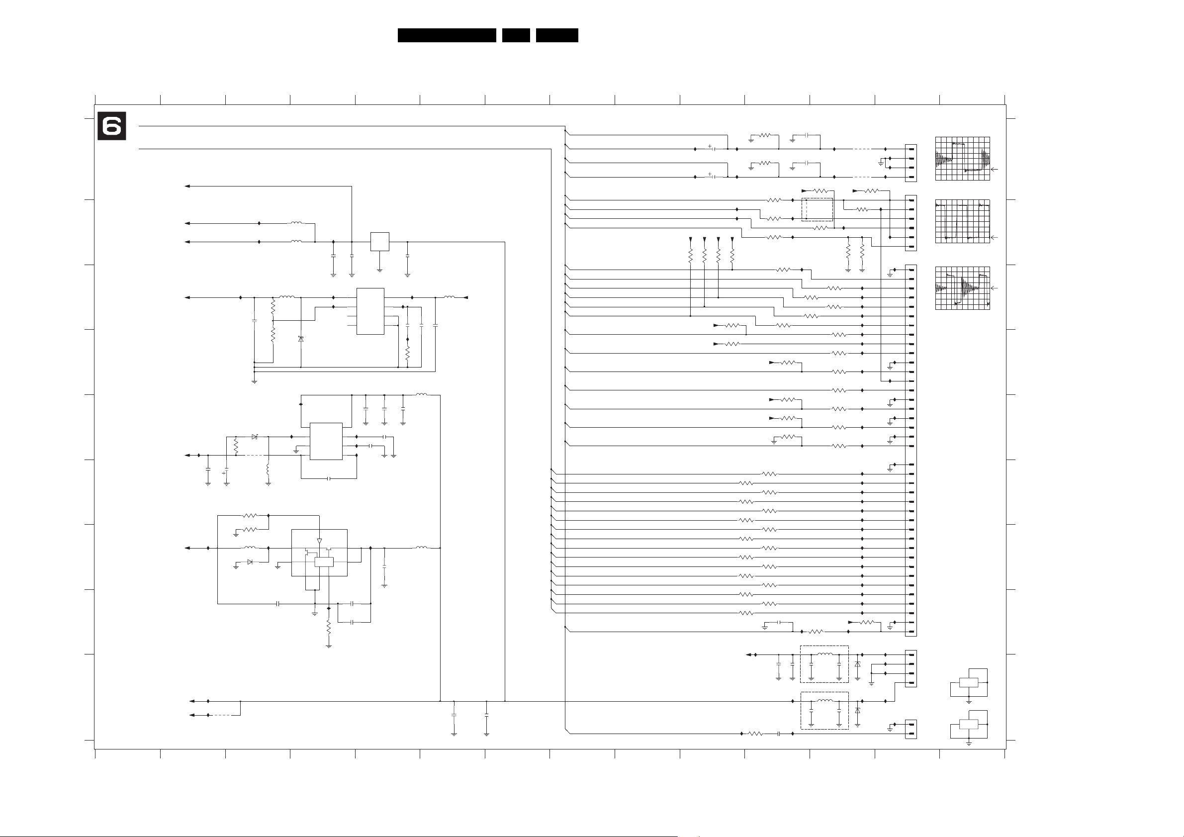
Electrical Diagrams and Print-Layouts
Servo Board: Power, Connectors
26VAD 8031 7.
A
B
C
D
E
F
G
H
I
1600-1 B13
1600-2 H13
1600-3 A13
1600-4 I13
1600-5 A13
1600-6 I14
1600-7 I14
2600 A12
2601 A12
2602 A11
2603 A11
2604 B12
2605 H11
2607 I11
2608 I6
2609 I11
2610 B5
2611 B4
2612 B4
2614 I6
2615 H3
2616 F2
2617 F2
2618 G5
2621 A10
2622 A10
2623 I11
2624 I12
2625 I12
2626 I11
2650 E5
2651 H4
2652 E5
2653 I11
2654 I6
2655 B4
2656 E5
2657 E5
2658 F4
2659 H4
2660 E5
2661 I11
2662 C6
2663 C5
2664 C5
2665 C3
3600 A12
3601 B12
3602 A11
3603 A11
3604 A12
3605 A11
3606 B11
3607 B12
3608 B11
3609 B12
3610 B12
3611 B10
3612 B10
3613 B10
3614 B10
3615-A C12
3615-B C12
3615-C C12
3615-D C12
3619 D12
3620 C10
3621 D10
3622 D12
3623 D12
3624 D11
3625 D12
3626 E12
3627 E11
3628 E12
3629 E11
3630 E12
3631-A F11
3631-B F11
3631-C F11
3631-D F11
3635-A G11
3635-B G11
3635-C F11
3635-D F11
3639-A G11
3639-B G11
3639-C G11
3639-D G11
3643-A H11
3643-B H11
3643-C G11
3643-D H11
3647 H12
3648 H12
3650-1 H9
3650-2 H9
3650-3 H9
3650-4 H9
3651-1 H9
3651-2 H9
3651-3 H9
3651-4 H9
3652-1 H9
3652-2 H9
3652-3 H9
3652-4 H10
3653-1 H10
3653-2 H9
3653-3 H9
3653-4 H9
3660 F3
3661 G3
3662 E3
3665 I11
3684 E11
3686 H4
3689 C11
1 2 3 4 5 6 7 8 9 10 11 12 13 14
CENTAURUS-DRAM-FLASHROM
{AUDIOL,AUDIOR,RX1_MASTER,DEBUG(11),TX1,TX2,HDASPN,CS0,CS1,HA0,HA1,HA2,HPDIAGN,HIRQ,HDACKN,IORDY,HRDN,HRWN,HDRQ,HRESET,IEC958,AUDIO_FRONT_L,AUDIO_FRONT_R}
HD(0:15)
A
3V3
A3V3
B
C
D3V3
+5V25
I629
I633
I687 I688 I689
22u
2665
3694
3693
5602
5603
5617
47u
3K9
1K2
6607
I634
2612
I690
SL12
22u
7606
L5970D
1
5
2
6
2611
100n
OUT
FB
SYNC
VREF
7603
LD1117DT33
OUT IN
COM
1
VCC
COMP
INH
GND
3
IN
2610
100n
2663
220p
2662
5616
+12V
22u
8
I691
4
3
7
22n
2664
2
OUT
I692
4K7
3692
D
5613
I630
8
SHDN_
E
I640
-5V
2617
22u
2616
3662
6606
SL12
1R
4612
47u
5604
10u
VCC
I686
7
LX
6
GND
5
OUT
2658
150p
ST735
REF
7605
2652
1
I665
2
I664
3
SS
I666
4
CC
2657
22u
22u
15n
2660
2656
10u
2650
100n
F
I652
3660
68K
3661
150K
D1V8
I648
G
5609
10u
6603
SK14
I647
4
5
2615
22u
LX I|O
SYNC
H
I
I650
+5V
I654
5VA
4604
GND
6
CTRL
7
7604
TEA1207T
FB
ILIM
OFF
2
8
I656
3686
330R
U_|D
DNIN
2651
2659
I667
3
1
2618
22u
22u
100n
5614
2654
22u
2608
100n
AUDIO_FRONT_R
AUDIOR
AUDIO_FRONT_L
AUDIOL
RX1_MASTER
TX2
TX1
DEBUG(11)
HDASPN
CS1
CS0
HA2
HA0
HPDIAGN
HA1
HIRQ
HDACKN
IORDY
HRDN
HRWN
HDRQ
HD(15)
HD(0)
HD(14)
HD(1)
HD(13)
HD(2)
HD(12)
HD(3)
HD(11)
HD(4)
HD(10)
HD(5)
HD(9)
HD(6)
HD(8)
HD(7)
HRESET
IEC958
2621
I684
47u
2622
I685
47u
+5V +5V +5V +5V
10K
10K
10K
3612
3613
3614
+5V
+5V
3611
3620
10K
3621
10K
3602
100K
I600 I601
3603 2603
100K
I603
3631-C
33R
3631-A
33R
3635-C
33R
3635-A
33R
3639-C
33R
3639-B
33R
3643-D
33R
3643-A
33R
I651
3665
100R
3605
1K
3606
470R
3608
1K
+5V
+5V
+5V
3631-D
45
33R
3631-B
27
33R
3635-D
45
33R
3635-B
27
33R
3639-D
45
33R
3639-A
18
33R
3643-C
36
33R
3643-B
27
33R
I657
I663
10K
36
18
36
18
36
27
45
18
+12V
I660
2605
10p
2653
2661
100n
3689
82R
3690
22R
3624
10K
3627
10K
3629
10K
3684
10K
22u
2602
10n
10n
+5V
I606
4601
I607
I609
I610
3615-C
36
3615-A
18
I646
2607
100n
I658
I661
3600
470R
ON BOTTOM
SIDE PCB
3607
470R
82R
82R
3648
82R
5615
100n
2623
EMI-FILTER
5607
2626
100n
EMI-FILTER
3615-D
45
3615-B
27
4610
I604 I605
4611
3604
+5V
10K
I674
3601
1K0
I608
3609
3610
220R
220R
I611
I612
82R
I613
I614
82R
I615
I616
3619
I668
82R
I617
3622
22R
I618
3623
82R
I619
3625
22R
I620
3626
82R
I621
3628
82R
I622
3630
22R
I623
I624
I625
I626
I627
I628
I631
I632
I636
I637
I638
I641
I642
I643
I644
I645
3647
+5V
I649
10K
I653
66046605
2624
100n
BZX384-C15
I659
100n
2625
MM3Z6V2
1600-3
I602
50
I675
49
I673
48
47
1600-5
46
45
44
43
I671
42
41
1600-1
I683
40
39
38
37
36
35
34
33
32
31
I679
30
29
I662
28
27
I678
26
25
I670
24
23
I669
22
21
I677
19
18
17
16
15
14
13
12
11
10
9
8
7
6
5
4
3
I672
2
1
1600-2
I680
+12V
I676
53
54
I538
55
56
I682
+5V
1600-4
I681
51
52
IC7604 Pin 4
A: DC, 1 V/Div, 1us/Div
IC7606 Pin 1
A: DC, 2 V/Div, 1us/Div
IC7605 Pin 7
A: DC, 2 V/Div, 1us/Div
1600-7
AA3E1A-G2K2L
AA3E1A-G2K2L
61
1600-6
57
62
63
58
59
64
60
aTR 15008_001
100903a
3690 C11
3691 F3
3692 D5
3693 D3
3694 C3
4601 B11
4604 I2
4605 B4
4610 A12
4611 A12
4612 E3
5602 B4
5603 B4
5604 F3
5607 I12
5609 G3
5613 D6
5614 G6
5615 H12
5616 C6
5617 C3
6603 G3
6604 I12
6605 I12
6606 E3
6607 D4
7603 B5
7604 G4
7605 E4
7606 C4
I538 I13
I600 A10
I601 A12
I602 A13
I603 A10
I604 A12
I605 A13
I606 A11
I607 B11
I608 B12
I609 B11
I610 C11
I611 C12
I612 C12
I613 C12
I614 C12
I615 C12
I616 C12
I617 D12
I618 D12
I619 D12
I620 E12
I621 E12
I622 E12
I623 F12
I624 F12
I625 F12
I626 F12
I627 F12
I628 F12
I629 B3
I630 E4
I631 F12
I632 G12
I633 B3
I634 B4
I636 G12
I637 G12
I638 G12
I640 E2
I641 G12
I642 G12
I643 G12
I644 H12
I645 H12
I646 H11
I647 G3
I648 G2
I649 H12
I650 I2
I651 H11
I652 F3
I653 H12
I654 I2
I656 H4
I657 B10
I658 I11
I659 I12
I660 I10
I661 I11
I662 D13
I663 B10
I664 E5
I665 E5
I666 E5
I667 G5
I668 D12
I669 E13
I670 E13
I671 B13
I672 H13
I673 A13
I674 B13
I675 A13
I676 I13
I677 E13
I678 D13
I679 D13
I680 H13
I681 I13
I682 I13
I683 B13
I684 A10
I685 A10
I686 E4
I687 C3
I688 C4
I689 C5
I690 C4
I691 C5
I692 D5
1 2 3 4 5 6 7 8 9 10 11 12 13 14
Page 27

Electrical Diagrams and Print-Layouts
Servo Board: Tray Motor Connections
1 2 3 4 5 6 7 8 9 10 11 12 13 14
A
B
C
D
E
F
G
H
I721
I722
I723
RX1_MASTER
L700
L701
L702
I715
L703
I716
I717
RX2
MRN
DEBUG(5)
DEBUG(6)
DEBUG(7)
DEBUG(10)
DEBUG(8)
DEBUG(12)
DEBUG(13)
DEBUG(4)
DEBUG(0)
DEBUG(1)
DEBUG(2)
DEBUG(3)
DEBUG(6)
DEBUG(7)
DEBUG(8)
DEBUG(5)
27VAD 8031 7.
OPU/CHEETAH_QD/DRIVERS/CENTAURUS/POWER-CONN
{RAD,SERVO-COMM,MOTO1,MRN,RX1_MASTER,TX1,A1,A2,CALF,VRIN,D1_TILTN,D2_TLN,D3_REN,D4_FEN,S1_MIRN,S2,FTC,MON1,MON2,RX2,TX2,PPNO,IRQN,PORN,T1,SCL,SDA,XDN,DRIVER-ON,FO-,FO+,VFOO-,VFOO+,RA,VRAOO,SL+,SL-,FOC+,FOC-,AUDIO_FRONT_L,AUDIO_FRONT_R,TR+,TR-,TRAYSW,EJECTKEY,SL,VSLOO,VMOTO1O}
DEBUG(0:13)
JTAG_TRST_CENT
JTAG_TDO_CENT
JTAG_TDI_CENT
JTAG_TMS
JTAG_TCK
JTAG_WE
JTAG_RY_BY
I720
3717
33R
3718
10K
3709
D3V3
10K
I700
I701
I702
I703
I704
I705
I707
I709
I711
I713
1702
AF2
15
14
I725
13
12
11
10
9
8
7
+5V
6
5
4
3
D3V3
2
I736
1
TRAYSW
AUDIO_FRONT_L
EJECTKEY
4700
AUDIO_FRONT_R
TR+
DEBUG(2)
DEBUG(1)
DEBUG(5)
DEBUG(4)
TR-
I706
I714
I710
I712
I708
I731
I732
I735
JTAG CONECTION
0001 I7
0002 I8
1700 B1
1702 F6
1703 C6
1705 E9
2700 I10
2701 I11
2702 I10
2703 I11
2704 I10
2705 I11
2706 I10
2707 I11
A
3702 H5
3703 H5
3704 H5
3705 H5
3706 I5
3707 I5
3708 C5
3709 C4
3710 C4
3711 C4
3712 C5
B
3713 B13
3714 B13
3715 B13
3716 B13
3717 C13
3718 D13
3719 D13
4700 F7
4701-A B2
4701-B B2
4701-C B2
4701-D C2
C
4702-A C2
4702-B C2
4702-C C2
4702-D D2
4703-A D2
4703-B D2
4703-C C2
4703-D C2
4704-A E2
4704-B E2
4704-C D2
4704-D E2
D
4705-A D2
4705-B F2
4705-C F2
4705-D E2
4706-A F2
4706-B F2
4706-C F2
4706-D D2
4707 F2
I700 C5
I701 D5
E
I702 D5
I703 D5
I704 D5
I705 D5
I706 C14
I707 D5
I708 C14
I709 D5
I710 C14
I711 E5
I712 C14
I713 E5
F
I714 C14
I715 H3
I716 H3
I717 H3
I718 I3
I719 I3
I720 C12
I721 E2
I722 E2
I723 F2
I725 F6
I731 C14
G
I732 C14
I735 D14
I736 H6
L700 G3
L701 G3
L702 H3
L703 H3
H
I718
DEBUG(9)
I719
DEBUG(11)
I
2700
10n
2702
10n
2704
10n
2706
10n
2701
2703
2705
2707
10n
10n
10n
10n
TR 15014_001
I
071003
1 2 3 4 5 6 7 8 9 10 11 12 13 14
Page 28

Electrical Diagrams and Print-Layouts
Layout Servo Board (Top Side)
28VAD 8031 7.
TR 15009_001
100903
Page 29

Electrical Diagrams and Print-Layouts
Layout Servo Board (Bottom Side)
29VAD 8031 7.
TR 15010_001
100903
Page 30

Electrical Diagrams and Print-Layouts
30VAD 8031 7.
Page 31

8. Alignments
In case of a change of DVD-M or PWB a readjustment is
necessary to align the OPU and PWB to each other.
8.1 Necessary Tools
– Personal computer with Windows 2000TM or Windows
TM
XP
– USB to ATAPI adapter, (standard computer equippment)
see figure 8-1.
– “Applicator software” (v2.85.00).
Alignments
EN 31VAD 8031 8.
Figure 8-2 , Applicator Software
Figure 8-1 , USB to ATAPI adapter
8.2 Adjustment Procedure
– Connect the basic engine to the USB to ATAPI adapter
– Power on the adapter
– Connect the USB connector of the adapter to the PC.
Note that the USB bus supports “Hot Plugging”. That
means the computer can already be switched on.
Alternatively you can connect the basic engine directly to
the IDE bus of a computer. In this case the adapter is not
necessary but the PC has to be switched off and must be
started up in order to detect the new drive on the IDE bus.
– Call up the applicator software, see figure 8-2
– Set the timeout to 50 seconds, see figure 8-3
– Run the “Adjust Laser Control” command, see figure 8-4.
– The "Status" indicator in the left section of the window has
to become green after successful adjustment.
After repairing the drive it should be tested at least with the
following discs:
1. LVP 12.01 (710409991731) test layer change on track 28
->31
2. DVD+R disc. Use Disc type Ricoh 4X DVD+R
- Record 1 minute
- press stop
- Open / close
- Play back recorded track
3. CD-RW low reflection audio disc. (7104 099 96581)
Figure 8-3 , Set Timeout
Figure 8-4 , Run Adjust Laser Control
Page 32

EN 32 VAD 80319.
Circuit Descriptions, Abbreviation List, and Data sh ee ts
9. Circuit Descriptions, Abbreviation List, and Datasheets
9.1 General
The VAD8031 module, also known as “AV3”, is a Video
Recorder Drive with an IDE interface intended for use in a
consumer DVD+RW/+R video recorder.
The video recorder engine performs all basic servo tasks. It
reads data from and writes data to the disc and controls all
functions like tray control, start/stop the disc, tracking, jumping
and communicating to the host.
9.2 Overall Block Diagram
OPU 67.66
BMC12S
Laser
(SZA1016)
Brush-less
Motordriver
3D
BA5995FM
BA5995FM
Op-amps
Laser
DVD
PCS
CD
EEPROM
Laser driver
EL6295
PAEDIC
Mechanically, the module consists of a motorized tray loader
that contains the dual laser optical pickup unit and a PCBA that
contains all the electronics needed to control the drive and
interfacing to the MPEG encoder/decoder back-end
application.
There is a temperature sensor included in the drive that
prevents malfunction or destruction of the drive in case the
temperature inside the drive gets too high.
Laconic
Cheetah-M
Sync
DRAM
Digital Backend
CENTAURUS
2MB
Flash
ROM
IDE
BA5944FP
Tilt Motor
driver
This section describes briefly the functional behaviour of the
engine. It performs all basic servo functions:
• It reads data from the disc,
• It writes data to the disc,
• It controls all other functions like tray control, start/stop the
disc, tracking, jumping, and communication to the host.
Optional tilt backup
9.3 Centaurus
Centaurus Basic Functions Block Diagram
Channel
Codec
Analogue
Servo
Controller
Analogue
Figure 9-2
Manager
Control
Processor
Buffer
Figure 9-1 Block diagram
The Centaurus, IC7500 is a highly integrated IC that controls all
the functions of the drive. It interfaces via the IDE to the MPEG
back-end and incorporates the following functions:
• CD/DVD channel decoder/encoder
• CD/DVD data block decoder/encoder
• Buffer Manager
• Digital Servo processor using digital signal processor.
• Drive System microprocessor based on MIPS core.
The MIPS microcontroller uses Flash ROM for the firmware
and SRAM to execute the program. SDRAM is provided for the
encoding/decoding function block of centaurus. 2 MBytes of
data buffer size is available inside the IC for data storage.
9.4 Cheetah
The Cheetah, IC7201 is an analogue pre-processing for the
diode signals coming from the OPU. It contains an amplifier
with programmable gain that amplifies the RF signal to adapt
the output for the different reflectivity of the various discs. The
tracking signals are filtered and normalized. In addition the IC
contains a timing circuit for the sample and hold circuits and for
switching the various blocks between read and write.
Supporting functions such as laser control and offset control
are incorporated. Communication to and from the IC is based
on a fast two-wire serial bus that works according to the I2C
interface protocol.
Page 33

Circuit Descriptions, Abbreviation List, and Datasheets
9.5 Laconic
The main function of the LACONIC, IC7300 is to control the
laser power. The IC forms a closed control loop in combination
with the Elantec located on the OPU. It compensates aging and
temperature of the laser. Furthermore it forms a fingerprint
correction loop. It also acts as bridge between IIC and serial
bus of the Elantec laser driver on the OPU.
9.6 Optical Pick-up Unit
The OPU66 is a dual laser Optical Pick-up Unit for DVD+RW/
+R. It consists of a 3-D actuator for focusing, redial tracking and
tilt correction.
• 650nm laser for DVD
• 780nm laser for CD
On the interconnecting flex several electrical components are
mounted.
• Elantec programmable laser diode power
driver
• Paedic integrated photo detector with
programmable gain pre-amplifier
• Eeprom containing a number of values
representing adjustments belonging to
the OPU.
EN 33VAD 8031 9.
The laser control and diode signal processor ICs together with
an EEPROM are mounted on the OPU flex.
The laser control IC generates the DVD laser read and writing
signals needed for reading DVD discs and writing DVD+RW /
+R discs (write strategies of DVD+RW / +R discs).
The diode signal processor is an analogue pre-processor
adapted for the CD and CD-R / RW read function.
The EEPROM contains information about writing current,
writing strategies and other parameters belonging to the OPU.
9.7 Motor and Servo drivers
A Servo Driver is implemented to control the sledge. Several
motor driver ICs are incorporated to control the Tray, Disc and
Turntable motors,
Driver ICs are incorporated for control of the:
• Actuator
•Disc Motor
• Sledge Motor
•Tray Motor
Page 34

EN 34 VAD 80319.
Circuit Descriptions, Abbreviation List, and Data sh ee ts
9.8 ICs Servo Board
IC7105, LM75A: Servo Board, Temperature Sensor
Pin description
PIN SYMBOL DESCRIPTION
1 SDA Digital I/O. I2C serial bi-directional data line.
Open Drain.
2 SCL Digital input. I2C serial clock input.
3 OS Overtemp Shutdown output. Open Drain.
4 GND Ground. To be connected to the system
ground.
5 A2 Digital input. User-defined address bit2.
6 A1 Digital input. User-defined address bit1.
7 A0 Digital input. User-defined address bit0.
8 V
CC
Power supply.
SIMPLIFIED BLOCK DIAGRAM
V
CC
BIAS
REFERENCE
BAND–GAP
TEMP
SENSOR
OSC
POWER–ON
RESET
LOGIC CONTROL AND INTERFACE
A2 A1 A0 SCL
SIGMA–DELTA
A–TO–D
CONVERTER
11–BIT
SDA
POINTER
REGISTER
COUNTER
TIMER
COMPARATOR
/ INTERRUPT
GND
CONFIGURATION
REGISTER
TEMPERATURE
REGISTER
TOS
REGISTER
THYST
REGISTER
OS
SL01389
Page 35

Circuit Descriptions, Abbreviation List, and Datasheets
IC7201, TZA1039HL: Servo Board, Analogue Preprocessor
BLOCK DIAGRAM
WRF
RFPIN
RFNIN
VDD1 VDD2 VSS1 VSS2
s/d
GND1
GND2
mux
GNDD
VSSD
RF-AMP
EN 35VAD 8031 9.
RFP
RFN
RF-REF
CALF
A1,A2
RRF
LASP
VIA..VIH
VREF
EFMDP
EFMDN
EFMCP
EFMCN
Input
Circuit
EFMTIM
s/d
S&H
to ALF A
and NORM
Gain
V I
LPF
Offset
Control
DPD
FTC
mux
L,R
BET A
ALF A
NORM
MON
PP-Processor
CCALF
CA1,CA2
ALF A
TS1
TS2
D1..D4
S1,S2
XDN
CMPP
MON1
MON2
PPN
FTC
CFTC
R/W
TIMOUT
VDDL
MI
LD
RREF
Laser
Control
r/w
control
currents
DACs
bandgap
reference
control
switches
Registers
+
Logic
Serial Bus
Interface
2
IC
Interface
POR
SIDA
SICL
SILD
SERTST
SROUT
SDA
SCL
TEST
Page 36

EN 36 VAD 80319.
Circuit Descriptions, Abbreviation List, and Data sh ee ts
PINNING
SYMBOL PIN DESCRIPTION
VIH 1 Satelite segment H input
GND1 2 Ground
VIC 3 Central segment C input
VIB 4 Central segment B input
GND1 5 Ground
RFNIN 6 Inverse differential RF input
RFPIN 7 Differential RF input
VDD1 8 Positive supply
VID 9 Central segment D input
VIA 10 Central segment A input
VDD1 11 Positive supply
VIE 12 Satelite segment E input
VIG 13 Satelite segment G input
R/W 14 External Read/Write signal input
N.C. 15 Not connected
N.C. 16 Not connected
N.C. 17 Not connected
TIMOUT 18 EFMTIM test output
VSSD 19 Negative supply
EFMCN 20 Inverse EFM clock input
EFMCP 21 EFM clock input
EFMDN 22 Inverse EFM data input
EFMDP 23 EFM data input
GNDD 24 Ground
SDA 25 Data input/output I2C
SCL 26 Clock input I2C
N.C. 27 Not connected
FTC 28 FTC output
CFTC 29 FTC high pass lter capacitor
TS2 30 Tilt sensor input current
TS1 31 Tilt sensor input current
SILD 32 Strobe line of serial bus interface
N.C. 33 Not connected
SIDA 34 Data line of serial bus interface
SICL 35 Clock line of serial bus interface
VDD2 36 Positive supply voltage
GND2 37 Supply ground
RFP 38 RF output voltage, positive
RFN 39 RF output voltage, negative
VSS2 40 Negative supply voltage
RFREF 41 Reference voltage for differential
RF output common mode level
PPNO 42 Output PP voltage
SYMBOL PIN DESCRIPTION
N.C. 43 Not connected
N.C. 44 Not connected
SERTST 45 Enable test mode (Tie to GND for
normal operation)
VSSD 46 Negative supply voltage
GNDD 47 Supply ground
CA1 48 Beta circuit external capacitor
CA2 49 Beta circuit external capacitor
CCALF 50 Beta circuit external capacitor
VSS1 51 Negative supply voltage
RREF 52 Reference resistor to VSS
GND1 53 Supply ground
CMPP 54 MPP external capacitor
VDD1 55 Positive supply
MON1 56 Monitor output voltage
MON2 57 Monitor output voltage
S2 58 Servo output current
S1 59 Servo output current
D4 60 Servo output current
D3 61 Servo output current
D2 62 Servo output current
D1 63 Servo output current
XDN 64 X-position output voltage
CALF 65 RF average level signal
A2 66 RF bottom level signal
A1 67 RF top level signal
SROUT 68 shift register output for register
test mode
ALFA 69 alfa output current
LASP 70 laser power setpoint signal
TEST 71 Test output
N.C. 72 Not connected
MI 73 Monitor input for laser
LD 74 Drive current for laser
VDDL 75 Laser supply voltage
RRF 76 Single-ended RF read input
WRF 77 Single-ended RF writeinput
VSS1 78 Negative supply
VREF 79 PDIC reference voltage output
VIF 80 Satelite segment F input
Page 37

Circuit Descriptions, Abbreviation List, and Datasheets
IC7300, TZA1042: Servo Baord, Laser Power Controller
Block diagram
EN 37VAD 8031 9.
DRAFT
Page 38

EN 38 VAD 80319.
Circuit Descriptions, Abbreviation List, and Data sh ee ts
Pin description
Symbol Pin Type Drive
Description
/Thr.
AEZ 1 I hypdT Alpha Error Zero/Alpha SetZero
V
V
DDD3
SSD3
2 P - Digital Pad Supply
3 P - Digital Pad Supply
CLOCKOUT 4 T M Buffered Oscillator Output
OSCO 5 AO A Output of inverting Amplifier that forms oscillator
OSCI 6 AI A Input of inverting Amplifierthat forms oscillator
TEST1D 7 I pd T Test pin
AMEAS 8 AI A Alpha Measure – valueof measured disk writing
quality
V
V
DDA1
SSA1
9 P - Analogue Supply
10 P - AnalogueSupply
LASP 11 AO A Laser Power – indicates power level
VREFL 12 AO A Bandgap Voltage Reference ground connection
VREFH 13 AO A Bandgap VoltageReference output
VDEL 14 AI A Voltage input for Delta “laser power”
VTHR 15 AI A Voltage input for Threshold“laser power”
VOPUREF 16 AO A Reference Voltage for OPU
VREFIN 17 AI A Input Reference Volt age for Vthr and Vdel
V
V
DDA2
SSA2
18 P - AnalogueSupply
19 P - AnalogueSupply
TEST1A 20 AB A Test pin
IAPCW 21 AO A Current Output of Delta Reference
IAPCR 22 AO A Current Output of ThresholdReference
TEST2A 23 AB A Test pin
ENR2 24 T M Programmable Output Flag
ENR1 25 B pd M/T Device Initialisation/Programmable Output Flag (must
be drivento VDD during reset)
DVDCD 26 T M Programmable Output Flag for indicating DVD/CD
mode
HILO 27 T M Programmable Output Flag for indicating High/Low
reflectivity
V
V
SSD1
DDD1
28 P - Digital Pad Supply
29 P - Digital Pad Supply
BUSY 30 B M/T Busy Enable input from Elantec / Board test IO
SEN 31 B M/T Serial Enable output to Elantec / Board test IO
SDIO 32 B M/T Serial datainput output from/to Elantec/ Board test IO
SCLK 33 B M/T Busy Enable input from Elantec/ Board test IO
WSB 34 B M/T Write Strategy Bank – output contr ols OPU write
switching / Board test IO
Page 39

Circuit Descriptions, Abbreviation List, and Datasheets
EN 39VAD 8031 9.
Pin description
Symbol Pin Type Drive
…continued
Description
/Thr.
IRQN 35 OD M I nterrupt Request Not – active low interrupt request
OSTR 36 I hypdT OPC Strobe – request step in alpha setpoint / Board
test input
RESETN 37 I hypdT Reset Not – active low reset input
RWN 38 B M/T Read/Write not– indicatespower setpoints/Board test
IO
V
V
SSD2
DDD2
39 P - Digital Core Supply
40 P - Digital Core Supply
BANK 41 I hypdT CAV setpoint switching input signal / Board test IO
TEST2D 42 I pd T Test pin
SDA 43 BOD M/T
SCL 44 I T
[1] All supply pins mustbe connected to thesame external power supply voltage
[2] All inputs are 5V tolerant – i.e. they will drive the supply voltage (3.0-3.6V), but will work correctly
when interface to a 5V drive device
[3] The pin type definitionis given below:
I2C Serial Data
I2C Serial Clock
PinType Definition Table
Type Definition
I input
O output
OD open drain
B bi-directional
BOD bi-directional
open drain
T tri-state output
AI analog input
AO analog output
AB analog
bi-directional
Ppower
connection
hy hysteresis on
input
pd hysteresis on
output
Page 40

EN 40 VAD 80319.
IC7402, SZA1015: Servo Board, Brushless Motor Controller
Circuit Descriptions, Abbreviation List, and Data sh ee ts
i.c.
ECR
EC
9, 31
8
7
n.c.
18
MUX
REFERENCE
MUX
INPUTS
OSCILLATOR
COSC ROSC
D
ADC
D
SZA1015
V
DD START
24
C
CURRENT
LIMITER
LIM
CURRENT
REFERENCE
23
THERMAL
SHUTDOWN
+
Σ
PWM COMMUTATION
+
EMF
REGENERATOR
HALL AMPLIFIERS
BIASREMFRLIM FG
REVERSE
BLOCKING
V
DDM
13, 16, 22
21
U
19
POWER
SWITCHES
15, 17, 20
DC-DC
CONVERTER
302928272625
WNWPVPUN VNUP
12332 456
V
SSA
V
14
W
GND
10
CP1
11
CP2
CAPY
12
MGT188
Page 41

Circuit Descriptions, Abbreviation List, and Datasheets
PINNING
SYMBOL PIN DESCRIPTION
V
SSA
BIAS 2 Hall element bias
ROSC 3 external resistor for internal oscillator
REMF 4 external resistor for EMF regeneration
RLIM 5 external resistor for current limiting
FG 6 frequency generator output
EC 7 output current control pin
ECR 8 output current control reference
i.c. 9 internally connected (leave
CP1 10 booster capacitor connection 1
CP2 11 booster capacitor connection 2
CAPY 12 booster output
V
DDM
W 14 motor terminal W
GND 15 ground supply
V
DDM
GND 17 ground supply
n.c. 18 not connected
V 19 motor terminal V
GND 20 ground supply
U 21 motor terminal U
V
DDM
START 23 start/stop control pin
V
DD
UP 25 positive Hall input U
UN 26 negative Hall input U
VP 27 positive Hall input V
VN 28 negative Hall input V
WP 29 positive Hall input W
WN 30 negative Hall input W
i.c. 31 internally connected (leave
COSC 32 external capacitor for internal oscillator
1 motor control ground supply
voltage pin
open-circuit)
13 motor supply voltage
16 motor supply voltage
22 motor supply voltage
24 system supply voltage
open-circuit)
EN 41VAD 8031 9.
Page 42

EN 42 VAD 80319.
Circuit Descriptions, Abbreviation List, and Data sh ee ts
IC7408,7409 BA5995: Servo Board, 4-channel BTL driver IC actuator and motor drive
23
24
25
26
27
28
+
PreV
+
CC
1
20k
10k
10k
+
2
+
+
20k
4
3
10k
10k
MUTE
ch1
5
Pin No.
Note) Symbol of + and (output of drivers) means polarity to input pin.
(For example if voltage of pin4 high, pin14 is high.)
Pin name
BIAS IN
1
OPIN1 (+)
2
OPIN1 ( )
3
OPOUT1
4
IN2
5
MUTE
6
STBY2
7
GND
8
PowV
9
10
PowV
11
V
O2
( )
12
V
O2
(+)
13
V
O1
( )
14
O1
(+)
V
Input for bias-amplifier
Non inverting input for CH1 OP-AMP
Inverting input for CH1 OP-AMP
Output for CH1 OP-AMP
Input for CH2
Input for CH1 mute control
Input for CH2 stand by control
Substrate ground
CC
1
V
CC
for CH1 power block
CC
2
V
CC
for CH2 power block
Inverted output of CH2
Non inverted output of CH2
Inverted output of CH1
Non inverted output of CH1
Function
22
20k
+
+
20k
STBY
ch2
7
6
21
8
Pin No.
15
16
17
18
19
20
21
22
23
24
25
26
27
28
STAND BY
ch1 / 3 / 4
PowV
CC
(ch1)
9
PowV
(ch3 / 4)
PowV
(ch2)
10
ch3
CC
+
LEVEL
SHIFT
LEVEL
SHIFT
+
CC
ch2
12
11
Pin name Function
V
O4
O4
V
V
O3
V
O3
PowV
STBY1
GND
OPOUT3
OPIN3 ( )
OPIN3 (+)
OPOUT4
OPIN4 ( )
OPIN4 (+)
PreV
Non inverted output of CH4
(+)
Inverted output of CH4
( )
Non inverted output of CH3
(+)
Inverted output of CH3
( )
V
CC
CC
for CH3/4 power block
3
Input for CH1/3/4 stand by control
Substrate ground
Output for CH3 OP-AMP
Inverting input for CH3 OP-AMP
Non inverting input for CH3 OP-AMP
Output for CH4 OP-AMP
Inverting input for CH4 OP-AMP
Non inverting input for CH4 OP-AMP
V
CC
CC
for pre block
10k 10k10k10k
+
10k 10k10k10k
ch4
+
+
LEVEL
SHIFT
LEVEL
SHIFT
+
+
ch1
14
Resistor unit : [ ]
10k10k
10k10k
10k
10k
10k
10k
+
13
15
16
17
18
19
20
Page 43

Circuit Descriptions, Abbreviation List, and Datasheets
M
m
IC7500, PNX7850: Servo Board, Channel Codec/Buffer Manager/Servo Processor and Controller
Nexperia PNX7850 conceptual block diagra
EN 43VAD 8031 9.
wobble
HF
motor
actuators
LF input
OPC input
ANALOG
EF
CHANNEL CODEC BUFFER
CD/DVD
WOBBLE
PROCESSOR
SIGNAL
CONDITION.
TACHO/MOTOR
CONTROL
SERVO DSP AND CONTROL PROCESSOR
SERVO
ACCELERATORS
OPC
EFM WRITE
CLOCK/DATA
GENERATOR
BIT
DETECTION
AND
DEMOD.
TELEMETRY
SERVO
DSP
CD/DVD
CHANNEL
ENCODE/
DECODE
WITH
ERROR
CORRECTION
DATA BLOCK
MICRO
INTERFACE
MIPS PR1910
INSTRUCTION
EXECUTION
UNIT
COPROCESSOR
ENCODE/
DECODE
PI-bus
INTERFACE
MANAGER
DRIVE INTERFACE
MICRO
INTERFACE
POWER
MANAGEMENT
CACHE
DEBUG SUPPORT
DEEPLY EMBEDDED
MEMORY
SDRAM
SDRAM
CONTROLLER
MEMORY
PROCESSOR
AUTOMATION
INTERRUPT
CONTROLLER
EJTAG
STATIC MEMORY
INTERFACE
ROM
CSS
UDMA66
HOST
INTERFACE
AUDIO
PROCESSOR
UART
CONFIG
GPIO
I2C
POWER CONTROL
AND RESET
host
audio
UART
GPIO
I2C
IC7603, LD1117: Servo Board, Voltage Regulator
BLOCK DIAGRAM
Flash
Page 44

EN 44 VAD 80319.
IC7604, TEA1207: Servo Board, DC/DC Converter
Block diagrama
Circuit Descriptions, Abbreviation List, and Data sh ee ts
LX
ILIM
4
2
N-type
POWER
FET
GND
I/V
CONVERTER
sense
FET
I/V
CONVERTER
CURRENT LIMIT
COMPARATORS
TEMPERATURE
PROTECTION
13 MHz
OSCILLATOR
P-type POWER FET
sense FET
START-UP
CIRCUIT
CONTROL LOGIC
AND
MODE GEARBOX
COUNTER
SYNC
GATE
568 1
SYNC U/D
SHDWN
DIGITAL CONTROLLER
TIME
INTERNAL
SUPPLY
TEA1207T
BAND GAP
REFERENCE
MGR665
3
7
UPOUT/DNIN
FB
PINNING
SYMBOL PIN DESCRIPTION
U/D 1 up-or-down mode selection
input; active LOW for up mode
ILIM 2 current limiting resistor
connection
UPOUT/DNIN 3 output voltage in up mode;
input voltage in down mode
LX 4 inductor connection
SYNC 5 synchronization clock input
GND 6 ground
FB 7 feedback input
SHDWN 8 shut-down input
Page 45

Circuit Descriptions, Abbreviation List, and Datasheets
IC7605, ST735: Servo Board, -5V Inverting PWM Regulator
SCHEMATIC DIAGRAM
EN 45VAD 8031 9.
PIN DESCRIPTION
Pin N˚ Symbol Name and Function
1 SHDN SHUT-DOWN Control (V
2V
REF
Reference Output Voltage
=ON GND=Shutdown
CC
3 SS Soft Start
4 CC Compensation Input
5V
OUT
Negative Output Voltage
6 GND Ground
7 LX Switch Output
8V
IC7606, L5970: Servo Board, Step Down Switching Regulator
IN
Positive Supply - Voltage Input
PINS FUNCTION
N. Name Description
1 OUT Regulator Output.
2 SYNC Master/slave synchronization.
3 INH A logical signal (active high) disables the device. If INH not used the pin must be grounded.
When it is open an internal pull-up disable the device.
4 COMP E/A output for frequency compensation.
5 FB Feedback input. Connecting directly to this pin results in an output voltage of 1.23V. An external
resistive divider is required for higher output voltages.
6V
7 GND Ground.
8V
3.3V V
REF
Unregulated DC input voltage.
CC
. No cap is requested for stability.
REF
Page 46

EN 46 VAD 80319.
Circuit Descriptions, Abbreviation List, and Data sh ee ts
9.9 Abbreviation list
ADC..............................Analogue to Digital Converter
ADIP.............................Address In Pre-groove
AGC..............................Automatic Gain Control
CD................................Compact Disc
CLV ..............................Constant Linear Velocity
DROPPI........................Dvd Rewritable Opu Pre-Processor IC
AM................................Amplitude Modulation
BE.................................Basic Engine
ComPair .......................Computer aided rePair
CD-DA..........................CD Digital Audio
CS ................................Chip Select
DAC..............................Digital to Analogue Converter
DAIO.............................Digital Audio Input Output
DENC...........................Digital Encoder
DFU..............................Direction For Use: description for the
end user
DNR..............................Dynamic Noise Reduction
DRAM...........................Dynamic RAM
DSD..............................Direct Stream Digital
DSP..............................Digital Signal Processing
DVD..............................Digital Versatile Disc
EEPROM......................Electrical Erasable Programmable
ROM
EFM..............................Eight to Fourteen bit Modulation
FDS..............................Full Diagnostic Software
HF.................................High Frequency
I2C................................Integrated Ic bus (signals at 5V level)
I2S................................Integrated Ic Sound bus (signals at
3.3V level)
IC..................................Integrated Circuit
IF..................................Intermediate Freq uency
IRQ...............................Interrupt ReQuest
LADIC...........................LAser Driver IC
LLD...............................Loss Less Decoder
LPCM ...........................Linear Pulse Code Modulation
LRCLK..........................Left/Right CLocK
MACE...........................Mini All Cd Engine
MPEG...........................Motion Pictures Experts Group
NC................................Not Connected
NVM .............................Non Volatile Memory: IC containing
DVD related data e.g. alignments
OPC..............................Optimum Power Calibration
OPU..............................Optical Pickup Unit
PCB..............................Printed Circuit Board (see PWB)
PCS..............................Position Control Sledge
PLL...............................Phase Locked Loop
PCM .............................Pulse Code Modulation
PCM_CLK ....................Audio system clock for DAC
PCM_OUTx..................Audio serial output data
PSU..............................Power Supply Unit
PWB.............................Printed Wiring Board (see PCB)
RAM .............................Random Access Memory
RGB..............................Red, Green and Blue colour space
ROM.............................Read Only Memory
RF.................................Radio Frequency
S2B...............................Serial to Basic engine, communication
bus between host- and servo
processor
SCL ..............................Serial Clock I2C
SCLK............................Audio serial bit clock
SDA..............................Serial Data I2C
SDRAM ........................Synchronous DRAM
SMC .............................Surface Mounted Components
S/PDIF..........................Sony Philips Digital InterFace
SPIDRE........................Signal Processing Ic for Dvd R
Ewritable
SRAM...........................Static Random Access Memory
STBY............................STandBY
SVCD ...........................Super Video CD
SW................................SoftWare
THD..............................Total Harmonic Distortion
TTL...............................Transistor Transistor Logic (5V logic)
uP................................. Microprocessor
VCD .............................Video CD
Y/C............................... Luminance (Y) and Chrominance (C)
signal
YUV.............................. Component video
Page 47
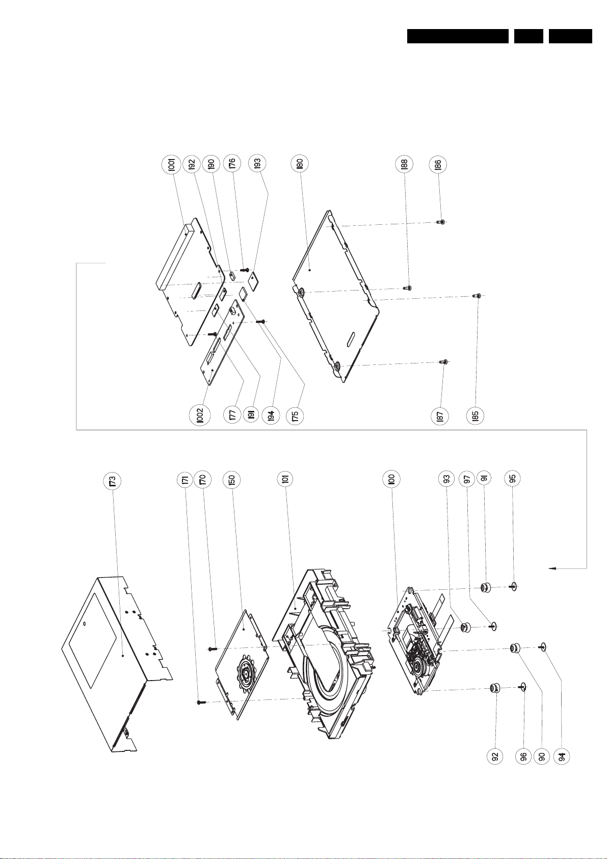
10. Spare Parts List
10.1 Exploded Views
Basic Engine
Spare Parts List
EN 47VAD 8031 10.
110903
TR 15011_001
Page 48

EN 48 VAD 803110.
Loader
Spare Parts List
110903
TR 15012_001
Page 49

DVD-M
Spare Parts List
EN 49VAD 8031 10.
TR 15013_001
110903
Page 50

EN 50 VAD 803110.
Spare Parts List
Basic Engine VAD8031
Various
7104 099 91731 LVP 12.01 MARGINAL DISC
7104 099 96581 CD-RW LOW REFLECTION
10-12 3104 148 01500 SLEDGE MOTOR ASSY
0090 3104 144 03901 SUSPENSION
0091 3104 144 03901 SUSPENSION
0092 3104 144 03901 SUSPENSION
0093 3104 144 03901 SUSPENSION
0094 3104 140 40622 DVDM MOUNTING SCREW
0095 3104 140 40622 DVDM MOUNTING SCREW
0096 3104 140 40622 DVDM MOUNTING SCREW
0097 3104 140 40622 DVDM MOUNTING SCREW
0100 9305 022 83001 DVDM 8031/01 (AV3)
0101 3122 487 90041 LOADER ASSY
0125 3104 144 10121 TRAY MOTOR BELT
0147 3104 144 04272 TRAY
0150 3122 487 90021 CLAMPER PLATE
1002 3104 128 09061 LOADER TRAY MOTOR
8000 3104 157 12231 FLEX CONNECTION
AUDIO DISC
ASSY
WIRES (ALL)
PCB Assy 4343 Data 3
Various
1100 2422 025 17821 CON H 45P F 0.50
1302 2422 543 01025 Crystal 16.93 MHz
1400 2422 025 17361 CON BM H 9P
1401 2422 025 17264 CON BM H 11P
1600 2422 033 00396 SOC COMBI H 56P
1702 2422 025 17359 CON BM H 15P
2100 2238 586 59812 100nF 20-80% 50V 0603
2101 4822 126 13883 220pF 5% 50V
2102 2238 586 59812 100nF 20-80% 50V 0603
2103 2020 552 94427 100pF 5% 50v 0603
2104 2238 586 59812 100nF 20-80% 50V 0603
2105 2238 586 59812 100nF 20-80% 50V 0603
2106 2238 586 59812 100nF 20-80% 50V 0603
2107 2022 552 05635 22µF 16V X5R 10%
2108 2238 586 59812 100nF 20-80% 50V 0603
2206 2238 586 59812 100nF 20-80% 50V 0603
2207 2238 586 59812 100nF 20-80% 50V 0603
2209 2238 586 59812 100nF 20-80% 50V 0603
2210 2238 586 59812 100nF 20-80% 50V 0603
2211 2238 586 59812 100nF 20-80% 50V 0603
2212 2238 586 59812 100nF 20-80% 50V 0603
2213 2238 786 56642 27nF 16V 0603 X7R 10%
2214 5322 126 11583 10nF 10% 50V 0603
2215 5322 126 11583 10nF 10% 50V 0603
2217 3198 017 34730 47nF 16V 0603
2218 5322 126 11583 10nF 10% 50V 0603
2219 2238 586 59812 100nF 20-80% 50V 0603
2220 2238 586 59812 100nF 20-80% 50V 0603
2221 2238 586 59812 100nF 20-80% 50V 0603
2222 2238 586 59812 100nF 20-80% 50V 0603
2223 2238 586 59812 100nF 20-80% 50V 0603
2300 2238 586 59812 100nF 20-80% 50V 0603
2301 2238 586 59812 100nF 20-80% 50V 0603
2302 2238 586 59812 100nF 20-80% 50V 0603
2303 4822 122 33752 15pF 5% 50V
2304 4822 122 33752 15pF 5% 50V
2305 2238 916 15641 22nF 10% 25V 0603
2306 2238 586 59812 100nF 20-80% 50V 0603
2307 2238 586 59812 100nF 20-80% 50V 0603
2310 2238 586 59812 100nF 20-80% 50V 0603
2311 5322 126 11578 1nF 10% 50V 0603
2312 4822 122 33752 15pF 5% 50V
2400 2238 586 59812 100nF 20-80% 50V 0603
2401 2238 586 59812 100nF 20-80% 50V 0603
2403 2238 586 59812 100nF 20-80% 50V 0603
2405 2238 586 59812 100nF 20-80% 50V 0603
2406 2238 586 59812 100nF 20-80% 50V 0603
2407 2238 586 59812 100nF 20-80% 50V 0603
2409 2238 586 59812 100nF 20-80% 50V 0603
2411 2020 552 94427 100pF 5% 50v 0603
2412 2238 586 59812 100nF 20-80% 50V 0603
2413 2238 586 59812 100nF 20-80% 50V 0603
2414 5322 126 11583 10nF 10% 50V 0603
2415 2238 916 15641 22nF 10% 25V 0603
2417 2238 586 59812 100nF 20-80% 50V 0603
2418 4822 126 14238 2.2nF 50V 0603
2419 4822 126 14238 2.2nF 50V 0603
2420 4822 126 14238 2.2nF 50V 0603
2421 4822 126 13193 4.7nF 10% 63V
2426 4822 126 14043 1µF 20% 16V
2427 2238 586 15628 2.7nF 10% 50V 0603
2430 2238 586 59812 100nF 20-80% 50V 0603
2431 4822 124 23002 10µF 20% 16V
2432 2238 586 59812 100nF 20-80% 50V 0603
2433 2022 552 05636 10µF 1210 X5R 16V 10%
2434 4822 126 14238 2.2nF 50V 0603
2435 4822 126 14238 2.2nF 50V 0603
2436 4822 126 14238 2.2nF 50V 0603
2438 2238 586 59812 100nF 20-80% 50V 0603
2440 2238 586 59812 100nF 20-80% 50V 0603
2441 2238 586 59812 100nF 20-80% 50V 0603
2442 2022 552 05635 22µF 16V X5R 10%
2443 2022 552 05635 22µF 16V X5R 10%
2444 2022 552 05616 4.7µF 6.3V 0805 X5R
2445 2238 586 59812 100nF 20-80% 50V 0603
2500 2238 586 59812 100nF 20-80% 50V 0603
2501 2238 586 59812 100nF 20-80% 50V 0603
2502 2238 586 59812 100nF 20-80% 50V 0603
2503 4822 126 13879 220nF 20% 16V
2504 5322 126 11578 1nF 10% 50V 0603
2505 5322 126 11583 10nF 10% 50V 0603
2506 5322 126 11583 10nF 10% 50V 0603
2507 5322 126 11582 6.8nF 10% 63V
2509 4822 126 13881 470pF 5% 50V
2511 4822 126 13881 470pF 5% 50V
2512 4822 126 13881 470pF 5% 50V
2514 2238 586 59812 100nF 20-80% 50V 0603
2515 4822 124 23002 10µF 20% 16V
2516 2238 586 59812 100nF 20-80% 50V 0603
2517 2238 586 59812 100nF 20-80% 50V 0603
2518 2238 586 59812 100nF 20-80% 50V 0603
2519 2238 586 59812 100nF 20-80% 50V 0603
2520 2238 586 59812 100nF 20-80% 50V 0603
2521 2238 586 59812 100nF 20-80% 50V 0603
2522 2238 586 59812 100nF 20-80% 50V 0603
2523 2238 586 59812 100nF 20-80% 50V 0603
2524 2238 586 59812 100nF 20-80% 50V 0603
2525 2238 586 59812 100nF 20-80% 50V 0603
2526 2238 586 59812 100nF 20-80% 50V 0603
2527 2238 586 59812 100nF 20-80% 50V 0603
2528 2238 586 59812 100nF 20-80% 50V 0603
2529 2238 586 59812 100nF 20-80% 50V 0603
2530 2238 586 59812 100nF 20-80% 50V 0603
2531 2238 586 59812 100nF 20-80% 50V 0603
2533 4822 124 23002 10µF 20% 16V
2534 2238 586 59812 100nF 20-80% 50V 0603
2536 2238 586 59812 100nF 20-80% 50V 0603
2538 4822 124 23002 10µF 20% 16V
2540 2238 586 59812 100nF 20-80% 50V 0603
2550 5322 126 11583 10nF 10% 50V 0603
2551 4822 122 33753 150pF 5% 50V
2552 4822 122 33753 150pF 5% 50V
2561 3198 017 34730 47nF 16V 0603
2562 3198 017 34730 47nF 16V 0603
2565 2238 586 59812 100nF 20-80% 50V 0603
2566 2238 586 59812 100nF 20-80% 50V 0603
2567 2238 586 59812 100nF 20-80% 50V 0603
2568 2238 586 59812 100nF 20-80% 50V 0603
2569 2238 586 59812 100nF 20-80% 50V 0603
2570 2238 586 59812 100nF 20-80% 50V 0603
2571 2238 586 59812 100nF 20-80% 50V 0603
2577 5322 126 11582 6.8nF 10% 63V
2578 4822 126 14549 33nF 16V 0603
2579 2238 586 59812 100nF 20-80% 50V 0603
2580 2022 552 05635 22µF 16V X5R 10%
2581 2238 586 59812 100nF 20-80% 50V 0603
2602 5322 126 11583 10nF 10% 50V 0603
2603 5322 126 11583 10nF 10% 50V 0603
2605 4822 122 33741 10pF 10% 50V
2607 2238 586 59812 100nF 20-80% 50V 0603
2608 2238 586 59812 100nF 20-80% 50V 0603
2610 2238 586 59812 100nF 20-80% 50V 0603
2611 2238 586 59812 100nF 20-80% 50V 0603
2612 2022 552 05635 22µF 16V X5R 10%
2615 2022 552 05635 22µF 16V X5R 10%
2616 4822 124 11131 47UF 6.3V
2617 2022 552 05635 22µF 16V X5R 10%
2618 2238 586 59812 100nF 20-80% 50V 0603
2621 4822 124 11131 47UF 6.3V
2622 4822 124 11131 47UF 6.3V
2623 2238 586 59812 100nF 20-80% 50V 0603
2624 2238 586 59812 100nF 20-80% 50V 0603
2625 2238 586 59812 100nF 20-80% 50V 0603
2626 2238 586 59812 100nF 20-80% 50V 0603
2650 2238 586 59812 100nF 20-80% 50V 0603
2651 2022 552 05635 22µF 16V X5R 10%
2652 2022 552 05635 22µF 16V X5R 10%
2653 2022 552 05635 22µF 16V X5R 10%
2654 2022 552 05635 22µF 16V X5R 10%
2656 2020 552 96637 10µF 6.3V 0805 X5R
2657 3198 017 31530 15nF 20% 50V 0603
2658 4822 122 33753 150pF 5% 50V
2659 2022 552 05635 22µF 16V X5R 10%
2660 2022 552 05635 22µF 16V X5R 10%
2661 2238 586 59812 100nF 20-80% 50V 0603
2662 2022 552 05635 22µF 16V X5R 10%
2663 4822 126 13883 220pF 5% 50V
2664 2238 916 15641 22nF 10% 25V 0603
2665 2022 552 05635 22µF 16V X5R 10%
2700 5322 126 11583 10nF 10% 50V 0603
2701 5322 126 11583 10nF 10% 50V 0603
2702 5322 126 11583 10nF 10% 50V 0603
2703 5322 126 11583 10nF 10% 50V 0603
2704 5322 126 11583 10nF 10% 50V 0603
2705 5322 126 11583 10nF 10% 50V 0603
2706 5322 126 11583 10nF 10% 50V 0603
2707 5322 126 11583 10nF 10% 50V 0603
3100 4822 117 13501 82Ω 5% 0.62W 0603
3101 4822 117 13501 82Ω 5% 0.62W 0603
3103 4822 051 30102 1kΩ 5% 0.062W
3104 4822 051 30101 100Ω 5% 0.062W
3105 4822 051 30102 1kΩ 5% 0.062W
3106 4822 051 30102 1kΩ 5% 0.062W
3107 4822 051 30102 1kΩ 5% 0.062W
3110 4822 051 30103 10kΩ 5% 0.062W
3111 4822 051 30103 10kΩ 5% 0.062W
3112 4822 051 30102 1kΩ 5% 0.062W
3113 4822 051 30102 1kΩ 5% 0.062W
3114 4822 117 12968 820Ω 5% 0.62W
3115 4822 051 30332 3.3kΩ 5% 0.062W
3116 4822 051 30152 1.5kΩ 5% 0.062W
3117 4822 051 30221 220Ω 5% 0.062W
3118 4822 051 30102 1kΩ 5% 0.062W
3200 4822 051 30101 100Ω 5% 0.062W
3201 4822 051 30101 100Ω 5% 0.062W
3203 4822 051 30103 10kΩ 5% 0.062W
3205 5322 117 13029 47kΩ 1% 0.063W 0603
3206 5322 117 13029 47kΩ 1% 0.063W 0603
3207 4822 051 30103 10kΩ 5% 0.062W
3208 4822 051 30103 10kΩ 5% 0.062W
3209 4822 117 12903 1.8kΩ 1% 0.063W 0603
3210 4822 117 12903 1.8kΩ 1% 0.063W 0603
3211 4822 117 12903 1.8kΩ 1% 0.063W 0603
3212 4822 117 12903 1.8kΩ 1% 0.063W 0603
3213 4822 051 30183 18kΩ 5% 0.062W
3214 4822 051 30273 27kΩ 5% 0.062W
3217 4822 051 30333 33kΩ 5% 0.062W
3301 4822 051 30103 10kΩ 5% 0.062W
3302 4822 117 12917 1Ω 5% 0.062W 0603
3303 4822 051 30151 150Ω 5% 0.062W
3309 4822 117 12903 1.8kΩ 1% 0.063W 0603
3315 4822 051 30339 33Ω 5% 0.062W
3316 4822 051 30103 10kΩ 5% 0.062W
3400 4822 051 30103 10kΩ 5% 0.062W
3401 4822 051 30103 10kΩ 5% 0.062W
3403 4822 051 30103 10kΩ 5% 0.062W
3404 4822 051 30103 10kΩ 5% 0.062W
3405 4822 051 30103 10kΩ 5% 0.062W
3406 4822 051 30102 1kΩ 5% 0.062W
3407 4822 051 30563 56kΩ 5% 0.062W
3408 4822 051 30103 10kΩ 5% 0.062W
3409 4822 051 30103 10kΩ 5% 0.062W
3410 4822 051 30563 56kΩ 5% 0.062W
3411 4822 051 30472 4.7kΩ 5% 0.062W
3412 4822 117 13501 82Ω 5% 0.62W 0603
3418 4822 117 12917 1Ω 5% 0.062W 0603
3420 4822 051 30123 12kΩ 5% 0.062W
3421 4822 117 12925 47kΩ 1% 0.063W 0603
3422 4822 051 30203 20K00 5% 0,062W
3423 4822 051 30103 10kΩ 5% 0.062W
3425 4822 117 13501 82Ω 5% 0.62W 0603
3426 4822 051 30562 5.6kΩ 5% 0.063W 0603
3427 2322 702 60184 180kΩ 5% 0603
3428 4822 051 30562 5.6kΩ 5% 0.063W 0603
3429 4822 051 30272 2.7kΩ 5% 0.062W
3430 2322 702 60511 510Ω 0603 RC21 PM5
3440 5322 117 13036 1.2kΩ 1% 0.063W 0603
3444 5322 117 13053 6.8kΩ 1% 0.063W 0603
3445 5322 117 13036 1.2kΩ 1% 0.063W 0603
3446 4822 117 11817 1.2kΩ 1% 1/16W
3447 5322 117 13053 6.8kΩ 1% 0.063W 0603
3450 5322 117 13053 6.8kΩ 1% 0.063W 0603
3451 4822 117 11817 1.2kΩ 1% 1/16W
3452 5322 117 13036 1.2kΩ 1% 0.063W 0603
3453 5322 117 13053 6.8kΩ 1% 0.063W 0603
3454 5322 117 13036 1.2kΩ 1% 0.063W 0603
3457 5322 117 13053 6.8kΩ 1% 0.063W 0603
3460 5322 117 13036 1.2kΩ 1% 0.063W 0603
3461 4822 117 11817 1.2kΩ 1% 1/16W
3462 5322 117 13053 6.8kΩ 1% 0.063W 0603
3464 5322 117 13036 1.2kΩ 1% 0.063W 0603
Page 51

Spare Parts List
EN 51VAD 8031 10.
3471 2322 702 60279 27Ω 5% 0.1W 0603
3472 4822 051 30123 12kΩ 5% 0.062W
3473 4822 051 30103 10kΩ 5% 0.062W
3474 4822 051 30123 12kΩ 5% 0.062W
3475 4822 051 30103 10kΩ 5% 0.062W
3477 4822 051 30123 12kΩ 5% 0.062W
3479 4822 051 30103 10kΩ 5% 0.062W
3480 4822 051 30103 10kΩ 5% 0.062W
3481 4822 117 12917 1Ω 5% 0.062W 0603
3482 4822 051 20108 1Ω 5% 0.1W
3483 4822 051 30103 10kΩ 5% 0.062W
3484 4822 051 30103 10kΩ 5% 0.062W
3485 4822 051 30103 10kΩ 5% 0.062W
3486 4822 051 30103 10kΩ 5% 0.062W
3487 4822 051 30102 1kΩ 5% 0.062W
3488 4822 051 30102 1kΩ 5% 0.062W
3489 2322 702 60279 27Ω 5% 0.1W 0603
3490 2322 702 60279 27Ω 5% 0.1W 0603
3491 2322 702 60279 27Ω 5% 0.1W 0603
3492 4822 051 30102 1kΩ 5% 0.062W
3493 4822 051 30471 470Ω 5% 0.062W
3494 4822 051 30471 470Ω 5% 0.062W
3495 4822 117 11817 1.2kΩ 1% 1/16W
3496 4822 117 11817 1.2kΩ 1% 1/16W
3497 4822 117 11817 1.2kΩ 1% 1/16W
3498 4822 117 11817 1.2kΩ 1% 1/16W
3499 4822 117 11817 1.2kΩ 1% 1/16W
3500 4822 051 30562 5.6kΩ 5% 0.063W 0603
3501 4822 051 30472 4.7kΩ 5% 0.062W
3502 4822 051 30272 2.7kΩ 5% 0.062W
3503 4822 051 30472 4.7kΩ 5% 0.062W
3504 4822 051 30472 4.7kΩ 5% 0.062W
3507 4822 051 30102 1kΩ 5% 0.062W
3508 4822 051 30102 1kΩ 5% 0.062W
3509 4822 051 30102 1kΩ 5% 0.062W
3510 4822 051 30682 6.8kΩ 5% 0.062W
3511 4822 051 30682 6.8kΩ 5% 0.062W
3512 4822 051 30682 6.8kΩ 5% 0.062W
3513 4822 051 30682 6.8kΩ 5% 0.062W
3514 4822 117 13632 100kΩ 1% 0603 0.62W
3515 4822 117 13632 100kΩ 1% 0603 0.62W
3516 4822 117 13525 24kΩ 1% 0.62W 0603
3517 4822 051 30103 10kΩ 5% 0.062W
3519 4822 051 30103 10kΩ 5% 0.062W
3520 4822 051 30103 10kΩ 5% 0.062W
3522 4822 117 12917 1Ω 5% 0.062W 0603
3524 4822 051 30103 10kΩ 5% 0.062W
3527 4822 051 30103 10kΩ 5% 0.062W
3529 4822 051 30222 2.2kΩ 5% 0.062W
3530 4822 051 30222 2.2kΩ 5% 0.062W
3531 4822 051 30479 47Ω 5% 0.062W
3532 4822 051 30479 47Ω 5% 0.062W
3541 4822 117 13576 NETW 4 X 33R 5% 1206
3542 4822 117 13576 NETW 4 X 33R 5% 1206
3543 4822 117 13576 NETW 4 X 33R 5% 1206
3545 4822 051 30339 33Ω 5% 0.062W
3546 4822 051 30339 33Ω 5% 0.062W
3547 4822 051 30334 330kΩ 5% 0.062W
3548 4822 051 30103 10kΩ 5% 0.062W
3550 4822 051 30102 1kΩ 5% 0.062W
3551 4822 051 30103 10kΩ 5% 0.062W
3560 4822 051 30101 100Ω 5% 0.062W
3562 4822 117 13526 150Ω 5% 0.63W
3574 4822 051 30103 10kΩ 5% 0.062W
3577 4822 051 30103 10kΩ 5% 0.062W
3578 4822 051 30332 3.3kΩ 5% 0.062W
3579 4822 051 30223 22kΩ 5% 0.062W
3580 4822 051 30472 4.7kΩ 5% 0.062W
3582 4822 051 30103 10kΩ 5% 0.062W
3583 4822 117 13526 150Ω 5% 0.63W
3584 4822 117 13526 150Ω 5% 0.63W
3585 4822 117 13526 150Ω 5% 0.63W
3586 4822 117 12968 820Ω 5% 0.62W
3587 4822 117 13526 150Ω 5% 0.63W
3588 4822 117 13526 150Ω 5% 0.63W
3589 4822 117 13526 150Ω 5% 0.63W
3591 4822 051 30151 150Ω 5% 0.062W
3592 4822 051 30151 150Ω 5% 0.062W
3593 4822 051 30151 150Ω 5% 0.062W
3594 4822 051 30151 150Ω 5% 0.062W
3595 4822 051 30151 150Ω 5% 0.062W
3596 4822 051 30151 150Ω 5% 0.062W
3597 4822 051 30151 150Ω 5% 0.062W
3598 4822 051 30151 150Ω 5% 0.062W
3599 4822 051 30151 150Ω 5% 0.062W
3602 4822 117 13632 100kΩ 1% 0603 0.62W
3603 4822 117 13632 100kΩ 1% 0603 0.62W
3604 4822 051 30103 10kΩ 5% 0.062W
3605 4822 051 30102 1kΩ 5% 0.062W
3606 4822 051 30471 470Ω 5% 0.062W
3607 4822 051 30471 470Ω 5% 0.062W
3608 4822 051 30102 1kΩ 5% 0.062W
3609 4822 051 30221 220Ω 5% 0.062W
3610 4822 051 30221 220Ω 5% 0.062W
3611 4822 051 30103 10kΩ 5% 0.062W
3612 4822 051 30103 10kΩ 5% 0.062W
3613 4822 051 30103 10kΩ 5% 0.062W
3614 4822 051 30103 10kΩ 5% 0.062W
3615 2350 035 10829 RST NETW SM ARV24 4X
3619 4822 117 13501 82Ω 5% 0.62W 0603
3620 4822 051 30103 10kΩ 5% 0.062W
3621 4822 051 30103 10kΩ 5% 0.062W
3622 4822 117 12139 22Ω 5% 0.062W
3623 4822 117 13501 82Ω 5% 0.62W 0603
3624 4822 051 30103 10kΩ 5% 0.062W
3625 4822 117 12139 22Ω 5% 0.062W
3626 4822 117 13501 82Ω 5% 0.62W 0603
3627 4822 051 30103 10kΩ 5% 0.062W
3628 4822 117 13501 82Ω 5% 0.62W 0603
3629 4822 051 30103 10kΩ 5% 0.062W
3630 4822 117 12139 22Ω 5% 0.062W
3631 2120 108 94458 RST NETW SM RAC16 4X
3635 2120 108 94458 RST NETW SM RAC16 4X
3639 2120 108 94458 RST NETW SM RAC16 4X
3643 2120 108 94458 RST NETW SM RAC16 4X
3647 4822 051 30103 10kΩ 5% 0.062W
3648 4822 117 13501 82Ω 5% 0.62W 0603
3650 4822 117 13578 4X10K 5% MNR14
3651 4822 117 13578 4X10K 5% MNR14
3652 4822 117 13578 4X10K 5% MNR14
3653 4822 117 13578 4X10K 5% MNR14
3660 2322 704 68203 82kΩ 0603 RC22H PM1
3661 2322 704 61504 150k 1% 0603
3662 4822 117 12917 1Ω 5% 0.062W 0603
3665 4822 051 30101 100Ω 5% 0.062W
3684 4822 051 30103 10kΩ 5% 0.062W
3686 4822 051 30331 330Ω 5% 0.062W
3689 4822 117 13501 82Ω 5% 0.62W 0603
3690 4822 117 12139 22Ω 5% 0.062W
3692 4822 051 30472 4.7kΩ 5% 0.062W
3693 4822 117 11817 1.2kΩ 1% 1/16W
3694 4822 051 30392 3.9kΩ 5% 0.063W 0603
3709 4822 051 30103 10kΩ 5% 0.062W
3717 4822 051 30339 33Ω 5% 0.062W
3718 4822 051 30103 10kΩ 5% 0.062W
4105 4822 051 30008 Jumper 0603
4108 4822 051 30008 Jumper 0603
4110 4822 051 30008 Jumper 0603
4112 4822 051 30008 Jumper 0603
4201 4822 051 30008 Jumper 0603
4303 4822 051 30008 Jumper 0603
4400 4822 051 20008 Jumper 0805
4402 4822 051 30008 Jumper 0603
4403 4822 051 20008 Jumper 0805
4404 4822 051 20008 Jumper 0805
4405 4822 051 20008 Jumper 0805
4406 4822 051 20008 Jumper 0805
4407 4822 051 20008 Jumper 0805
4413 4822 051 30221 220Ω 5% 0.062W
4415 4822 051 30008 Jumper 0603
4416 4822 051 20008 Jumper 0805
4419 4822 051 30008 Jumper 0603
4422 4822 051 30008 Jumper 0603
4427 4822 051 30008 Jumper 0603
4502 4822 051 30008 Jumper 0603
4525 4822 051 30008 Jumper 0603
4604 4822 051 30008 Jumper 0603
4610 4822 051 30008 Jumper 0603
4611 4822 051 30008 Jumper 0603
4612 4822 051 30008 Jumper 0603
4700 4822 051 30008 Jumper 0603
82R PM5
56R PM5 R
56R PM5 R
56R PM5 R
56R PM5 R
5101 2422 549 43062 Bead 600Ω at 100MHz
5102 2422 549 43062 Bead 600Ω at 100MHz
5103 2422 549 43062 Bead 600Ω at 100MHz
5104 3198 018 51090 10µH 10% 0603
5201 2422 549 43062 Bead 600Ω at 100MHz
5202 2422 549 43062 Bead 600Ω at 100MHz
5204 2422 549 43062 Bead 600Ω at 100MHz
5300 2422 549 43062 Bead 600Ω at 100MHz
5301 2422 549 43062 Bead 600Ω at 100MHz
5400 2422 536 00501 IND FXD SM D62LCB 10U
5405 2422 549 43062 Bead 600Ω at 100MHz
5406 2422 549 43062 Bead 600Ω at 100MHz
5501 2422 549 43062 Bead 600Ω at 100MHz
5502 2422 549 43062 Bead 600Ω at 100MHz
5504 2422 549 43062 Bead 600Ω at 100MHz
5602 2422 549 43062 Bead 600Ω at 100MHz
5603 2422 549 43062 Bead 600Ω at 100MHz
PM20 R
5604 2422 536 00501 D62LCB 10U PM20 R
5607 2422 549 45322 0603 EMI 100MHZ 150R R
5609 2422 536 00501 D62LCB 10U PM20 R
5613 2422 549 43062 Bead 600Ω at 100MHz
5614 2422 549 43062 Bead 600Ω at 100MHz
5615 2422 549 45322 EMI 100MHZ 150R R
5616 2422 549 43062 Bead 600Ω at 100MHz
5617 2422 536 00593 IND FXD SM D62LCB 47U
PM20 R
6100 4822 130 11397 BAS316
6401 9340 548 52115 PDZ5.1B
6603 9322 168 86685 SK14
6604 4822 130 11522 UDZ15B
6605 9322 159 72685 MM3Z6V2
6606 9322 189 14668 SL12
6607 9322 189 14668 SL12
7101 5322 130 60159 BC846B
7102 5322 130 60159 BC846B
7103 5322 130 60159 BC846B
7104 9340 547 21215 BSH205
7105 9352 697 76118 LM75ADP
7201 9352 714 71557 TZA1039HL
7300 9352 713 77157 TZA1042HL
7400 5322 209 82941 LM358D
7401 5322 209 82941 LM358D
7402 9352 656 66118 SZA1015TT BMC12
7405 4822 209 63709 LM324D
7408 9322 164 64668 BA5995FM
7409 9322 164 64668 BA5995FM
7500 9352 730 44557 PNX7850E_Z_M1D
7502 9322 186 84685 MAX6352SVUK
7503 3104 123 96850 IC FLASH ASSY DATA 3
7504 9322 166 67668 MT48LC4M16A2TG-7E
7603 4822 209 17398 LD1117DT33
7604 9352 610 38118 TEA1207T_N1
7605 9322 184 76668 ST735CD
7606 9322 191 07668 L5970D
Page 52

EN 52 VAD 803110.
Spare Parts List
 Loading...