

Page 1

DISCRETE SEMICONDUCTORS
DATA SH EET
ook, halfpage
M3D088
BAS19; BAS20; BAS21
General purpose diodes
Product specification
Supersedes data of 1999 May 26
2003 Mar 20
Page 2

Philips Semiconductors Product specification
General purpose diodes BAS19; BAS20; BAS21
FEATURES
• Small plastic SMD package
• Switching speed: max. 50 ns
• General application
• Continuous reverse voltage: max. 100 V; 150 V; 200 V
• Repetitive peak reverse voltage: max. 120 V; 200 V;
250 V
• Repetitive peak forward current: max. 625 mA.
APPLICATIONS
• General purpose switching in e.g. surface mounted
circuits.
DESCRIPTION
The BAS19, BAS20 and BAS21 are general purpose
diodes fabricated in planar technology, and encapsulated
in a small SOT23 plastic SMD package.
MARKING
TYPE NUMBER MARKING CODE
(1)
BAS19 JP∗
BAS20 JR∗
BAS21 JS∗
PINNING
PIN DESCRIPTION
1 anode
2 not connected
3 cathode
handbook, halfpage
21
2
n.c.
3
Fig.1 Simplified outline (SOT23) and symbol.
1
3
MAM185
Note
1. ∗ = p: Made in Hong Kong.
∗ = t: Made in Malaysia.
∗ = W: Made in China.
2003 Mar 20 2
Page 3

Philips Semiconductors Product specification
General purpose diodes BAS19; BAS20; BAS21
LIMITING VALUES
In accordance with the Absolute Maximum Rating System (IEC 60134).
SYMBOL PARAMETER CONDITIONS MIN. MAX. UNIT
V
V
I
F
I
FRM
I
FSM
P
T
T
RRM
R
tot
stg
j
repetitive peak reverse voltage
BAS19 − 120 V
BAS20 − 200 V
BAS21 − 250 V
continuous reverse voltage
BAS19 − 100 V
BAS20 − 150 V
BAS21 − 200 V
continuous forward current see Fig.2; note 1 − 200 mA
repetitive peak forward current − 625 mA
non-repetitive peak forward current square wave; Tj=25°C prior to
surge; see Fig.4
t=1µs − 9A
t = 100 µs − 3A
t = 10 ms − 1.7 A
total power dissipation T
=25°C; note 1 − 250 mW
amb
storage temperature −65 +150 °C
junction temperature − 150 °C
Note
1. Device mounted on an FR4 printed-circuit board.
2003 Mar 20 3
Page 4

Philips Semiconductors Product specification
General purpose diodes BAS19; BAS20; BAS21
ELECTRICAL CHARACTERISTICS
Tj=25°C unless otherwise specified.
SYMBOL PARAMETER CONDITIONS MAX. UNIT
V
F
I
R
C
d
t
rr
forward voltage see Fig.3
I
= 100 mA 1 V
F
I
= 200 mA 1.25 V
F
reverse current see Fig.5
BAS19 V
BAS20 V
BAS21 V
= 100 V 100 nA
R
= 100 V; Tj= 150 °C 100 µA
V
R
= 150 V 100 nA
R
V
= 150 V; Tj= 150 °C 100 µA
R
= 200 V 100 nA
R
V
= 200 V; Tj= 150 °C 100 µA
R
diode capacitance f = 1 MHz; VR= 0; see Fig.6 5 pF
reverse recovery time when switched from IF= 30 mA to
50 ns
IR= 30 mA; RL= 100 Ω; measured at
IR= 3 mA; see Fig.8
THERMAL CHARACTERISTICS
SYMBOL PARAMETER CONDITIONS VALUE UNIT
R
R
th j-tp
th j-a
thermal resistance from junction to tie-point 330 K/W
thermal resistance from junction to ambient note 1 500 K/W
Note
1. Device mounted on an FR4 printed-circuit board.
2003 Mar 20 4
Page 5
Philips Semiconductors Product specification
General purpose diodes BAS19; BAS20; BAS21
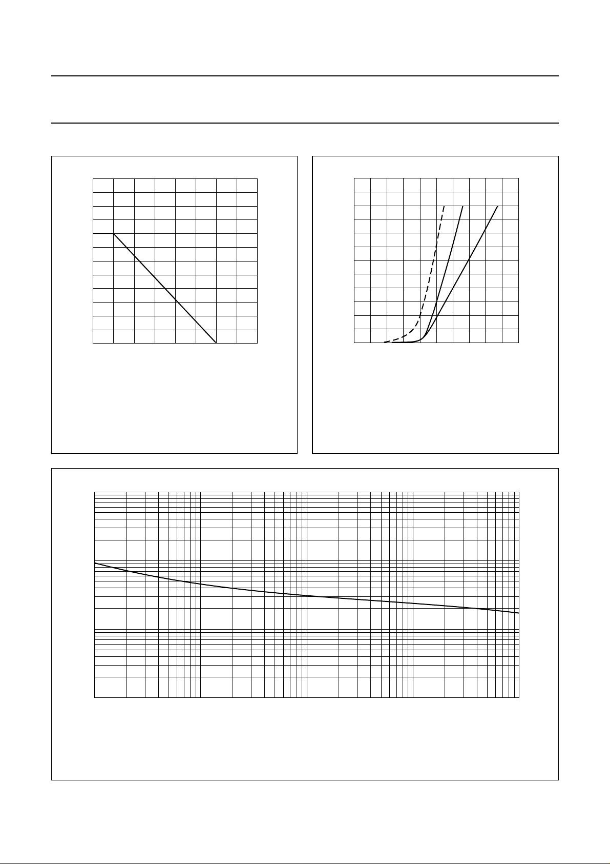
GRAPHICAL DATA
amb
MBG442
(oC)
300
handbook, halfpage
I
F
(mA)
200
100
0
0 100 200
Device mounted on an FR4 printed-circuit board.
T
Fig.2 Maximum permissible continuous forward
current as a function of ambient
temperature.
600
handbook, halfpage
I
F
(mA)
400
200
0
02
(1) Tj= 150°C; typical values.
(2) Tj=25°C; typical values.
(3) Tj=25°C; maximum values.
(1) (3)(2)
1
MBG384
VF (V)
Fig.3 Forward current as a function of forward
voltage.
2
10
handbook, full pagewidth
I
FSM
(A)
10
1
−1
10
1
Based on square wave currents.
Tj=25°C prior to surge.
Fig.4 Maximum permissible non-repetitive peak forward current as a function of pulse duration.
MBG703
10
2
10
3
10
tp (µs)
4
10
2003 Mar 20 5
Page 6
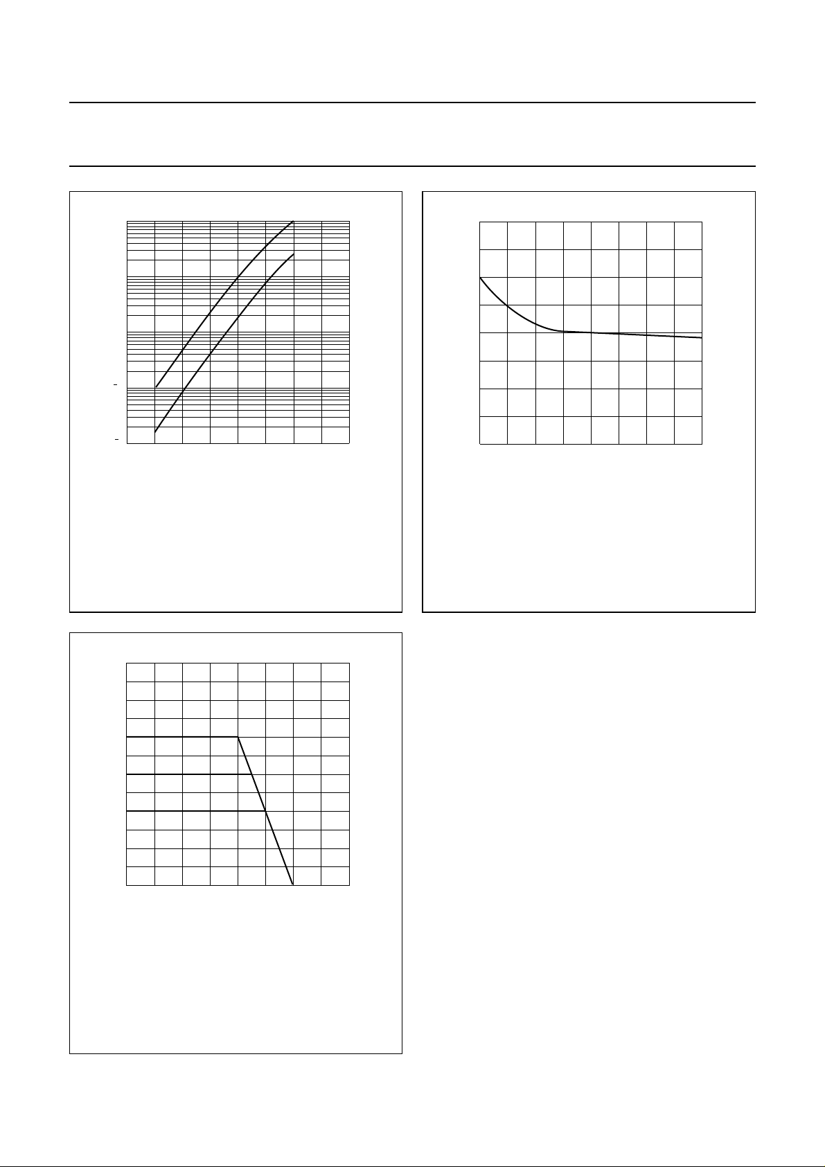
Philips Semiconductors Product specification
General purpose diodes BAS19; BAS20; BAS21
2
10
handbook, halfpage
I
R
(µA)
10
1
1
10
2
10
0
(1) VR=V
(2) VR=V
(1) (2)
; maximum values.
Rmax
; typical values.
Rmax
100
Tj (
MBG381
o
C)
Fig.5 Reverse current as a function of junction
temperature.
200
1.0
handbook, halfpage
C
d
(pF)
0.8
0.6
0.4
0.2
04862
f = 1 MHz; Tj=25°C.
MBG447
VR (V)
Fig.6 Diode capacitance as a function of reverse
voltage; typical values.
amb
MBG445
(oC)
300
handbook, halfpage
V
R
(V)
200
100
0
0 100 200
(1) BAS21.
(2) BAS20.
(3) BAS19.
(1)
(2)
(3)
T
Fig.7 Maximum permissible continuous reverse
voltage as a function of the ambient
temperature.
2003 Mar 20 6
Page 7

Philips Semiconductors Product specification
General purpose diodes BAS19; BAS20; BAS21
handbook, full pagewidth
R = 50SΩ
V = V I x R
RF S
(1) IR= 3 mA.
I
F
D.U.T.
SAMPLING
OSCILLOSCOPE
R = 50iΩ
MGA881
t
r
10%
V
R
90%
t
p
input signal
Fig.8 Reverse recovery voltage test circuit and waveforms.
t
I
F
t
rr
t
(1)
output signal
2003 Mar 20 7
Page 8

Philips Semiconductors Product specification
General purpose diodes BAS19; BAS20; BAS21
PACKAGE OUTLINE
Plastic surface mounted package; 3 leads SOT23
D
3
A
A
1
12
e
1
b
p
e
w M
B
E
H
E
detail X
AB
Q
L
p
X
v M
A
c
0 1 2 mm
scale
DIMENSIONS (mm are the original dimensions)
A
1
0.1
b
cD
p
0.48
0.15
3.0
0.38
0.09
IEC JEDEC EIAJ
2.8
1.4
1.2
e
E
1.9
REFERENCES
0.95
e
1
UNIT
A
max.
1.1
mm
0.9
OUTLINE
VERSION
SOT23 TO-236AB
2003 Mar 20 8
H
2.5
2.1
L
Qwv
p
E
0.55
0.45
0.15
0.45
0.2
0.1
EUROPEAN
PROJECTION
ISSUE DATE
97-02-28
99-09-13
Page 9

Philips Semiconductors Product specification
General purpose diodes BAS19; BAS20; BAS21
DATA SHEET STATUS
LEVEL
DATA SHEET
STATUS
(1)
PRODUCT
STATUS
(2)(3)
DEFINITION
I Objective data Development This data sheet contains data from the objective specification for product
development. Philips Semiconductors reserves the right to change the
specification in any manner without notice.
II Preliminary data Qualification This data sheet contains data from the preliminary specification.
Supplementary data will be published at a later date. Philips
Semiconductors reserves the right to change the specification without
notice, in order to improve the design and supply the best possible
product.
III Product data Production This data sheet contains data from the product specification. Philips
Semiconductors reserves the right to make changes at any time in order
to improve the design, manufacturing and supply. Relevant changes will
be communicated via a Customer Product/Process Change Notification
(CPCN).
Notes
1. Please consult the most recently issued data sheet before initiating or completing a design.
2. The product status of the device(s) described in this data sheet may have changed since this data sheet was
published. The latest information is available on the Internet at URL http://www.semiconductors.philips.com.
3. For datasheets describingmultipletype numbers,the highest-level productstatus determines thedata sheetstatus.
DEFINITIONS
DISCLAIMERS
Short-form specification The data in a short-form
specification is extracted from a full data sheet with the
same type number and title. For detailed information see
the relevant data sheet or data handbook.
Limiting valuesdefinition Limitingvalues givenare in
accordance with the Absolute Maximum Rating System
(IEC 60134). Stress above one or more of the limiting
values may cause permanent damage to the device.
These are stress ratings only and operation of the device
atthese orat anyother conditionsabovethose givenin the
Characteristics sectionsof the specification isnot implied.
Exposure to limiting values for extended periods may
affect device reliability.
Application information Applications that are
described herein for any of these products are for
illustrative purposes only. Philips Semiconductors make
norepresentation orwarrantythat suchapplications willbe
suitable for the specified use without further testing or
modification.
Life support applications These products are not
designed for use in life support appliances, devices, or
systems where malfunction of these products can
reasonably beexpected toresult inpersonal injury.Philips
Semiconductorscustomers usingorselling theseproducts
for use in such applications do so at their own risk and
agree to fully indemnify Philips Semiconductors for any
damages resulting from such application.
Right to make changes Philips Semiconductors
reserves the right to make changes in the products including circuits, standard cells, and/or software described or contained herein in order to improve design
and/or performance.When theproduct is infull production
(status ‘Production’), relevant changes will be
communicated via a Customer Product/Process Change
Notification (CPCN). Philips Semiconductorsassumes no
responsibility or liability for the use of any of these
products, conveys no licence or title under any patent,
copyright, or mask work right to these products, and
makes no representations or warranties that these
products are free from patent, copyright, or mask work
right infringement, unless otherwise specified.
2003 Mar 20 9
Page 10

Philips Semiconductors Product specification
General purpose diodes BAS19; BAS20; BAS21
NOTES
2003 Mar 20 10
Page 11

Philips Semiconductors Product specification
General purpose diodes BAS19; BAS20; BAS21
NOTES
2003 Mar 20 11
Page 12

Philips Semiconductors – a w orldwide compan y
Contact information
For additional information please visit http://www.semiconductors.philips.com. Fax: +31 40 27 24825
For sales offices addresses send e-mail to: sales.addresses@www.semiconductors.philips.com.
© Koninklijke Philips Electronics N.V. 2003
All rights are reserved. Reproduction in whole or in part is prohibited without the prior written consent of the copyright owner.
The information presented in this document doesnot formpart of any quotation or contract, isbelieved tobe accurate and reliable and may bechanged
without notice. No liability will be accepted by the publisher for any consequence of its use. Publication thereof does not convey nor imply any license
under patent- or other industrial or intellectual property rights.
Printed in The Netherlands 613514/04/pp12 Date of release: 2003 Mar 20 Document order number: 9397 75010961
SCA75
 Loading...