

Philips AZ-1009, AZ-1010 Service manual
Published by MS 9741 Service Audio Printed in The Netherlands Subject to modification
chapter
Technical Specification................................................2-1
Measurement setup.....................................................2-2
Controls & Connections...............................................2-3
Brief Operating Instructions....................................2-4 to 2-7
Warnings & Safety.......................................................2-8
Dismantling Instructions..........................................3-1 to 3-3
Service hints...........................................................3-4 to 3-6
CD - startup procedure ................................................3-7
Abbreviations CD-ICs ..................................................3-8
Service Test Program.................................................3-10
BLOCK DIAGRAM.......................................................4-1
WIRING DIAGRAM......................................................5-1
TUNER BOARD
schematic diagram ..................................................6-1
component layout....................................................6-2
adjustment table......................................................6-2
chapter
FRONT BOARD
component layout .................................................7-1
schematic diagram .................................................7-2
COMBI BOARD
component layout ................................................7-1, 7-4
schematic diagram CD part.....................................7-2
Recorder/Amplifier part............7-3
EXPLODED VIEWS
apparatus, drawing 1...............................................8-1
apparatus, drawing 2...............................................8-2
tape transport ..........................................................8-3
MECHANICAL PARTSLIST see Exploded views
ELECTRICAL PARTSLIST.........................................9-1 ff
TABLE OF CONTENTS
CS 49 101
AZ1009/00/05/17
© 4822 725 26015
CD Stereo Radio Recorder
CLASS 1
LASER PRODUCT
AZ1010/00/01/04/05/10
/11/11H/14/17
©
Copyright 1997 Philips Consumer Electronics B.V. Eindhoven, The Netherlands
All rights reserved. No part of this publication may be reproduced, stored in a retrieval
system or transmitted, in any form or by any means, electronic, mechanical, photocopying,
or otherwise without the prior permission of Philips.
Service Manual
DB
D
B
B
DYNAMIC
B
DYNAMIC
BASS
BASS
BOOST
BOOST
CD SYNCHRO START RECORDING
CD SYNCHRO START RECORDING
VO
VO
LUM
LUME
E
PAUSE
PAUSE
STOP.OP
STOP.O
EN
PEN
BASS REFLEX SPEAKER SYSTEM
BASS REFLEX SPEAKER SYSTEM
OPEN
OPEN
S
EA
S
E
R
A
C
R
H
C
H
PLAY
PLAY
R
EC
R
O
E
R
C
D
O
R
D
CD MODE
CD MODE
FM AM
FM AM
10
8
1
0
17
8
00
1
70
1
04
0
10
4
13
0
13
0
0
104
0
1
04
10
00
10
0
0
9
0
9
8
0
00
80
0
9
2
92
630
6
30
TU
TUN
N
IN
G
IN
8
8
G
88
53
0
5
3
0

TECHNICAL SPECIFICATION
General:
Mains voltage : 220V-230V / 50Hz for /00 /04 /14
230V-240V / 50Hz for /05 /10
110V-127V / 220V-240V /50Hz switchable for /01 /11 /11H
120V / 60Hz for /17
Battery : 9V ( 6xR20 )
Power consumption : ≤ 15W at maximum output power, ( ≤ 11W at 1/8 P
max
)
≤ 5W (typ. 2W) with source switch in
tape/off
Amplifier:
Power stage protection : temperature and shortcircuit
Output power mains : 2 x 1,4Wrms -1dB at 4Ω D=10%
battery : 2 x 2Wrms -1dB at 4Ω D=10%
Headphone : 3,5mm stereo jack, ≥ 20mW at 32Ω (≡ 0,8V at 32Ω ) D=10%
Frequency response : 30Hz - 16kHz ( typ. at volume set to -20dB, CD mode 0dB signal level ⇒use SBC429 )
Tone control DBB : +12dB ±3dB at 100Hz ( volume set to -20dB )
Tuner:
FM MW
Tuning range 87,5 - 108 MHz 522 - 1607 kHz
(520 - 1730 kHz for /17)
IF 10,7 MHz ± 20 kHz 468 kHz ± 3 kHz
Sensitivity Mono: 26dB S/N, m=30% ≤ 4 µV ( ≤ 2µV typ.) ≤ 4mV/m (≤ 1,5mV/m typ.)
-3 dB limiting point ≤ 5 µV ( ≤ 2µV typ.)
AFC capture range ±300kHz typ.
Distortion ≤ 7% (≤ 1% typ.) ≤ 7% (≤ 2,5% typ.)
RF=1mV ∆f=75kHz RF=100mV/m m=80%
Image rejection ratio ≥ 20dB (26dB typ.) ≥ 28dB
Channel separation at 1kHz ≥ 20dB (25dB typ.)
CD:
To be measured on phone socket with 100kΩ load.
Frequency response : 30 - 16.000 Hz -4dB
Signal/Noise ratio : ≥ 60dB
Distortion : 0.2% typ. at 1 kHz
Channel difference : ≤ 3dB at 1 kHz
Channel crosstalk : 40dB typ.
De emphasis : 0 or 15/50µs switched automatically by subcode on the disc
Laser
Output power : 500µW
Wave length : 780 ± 20 nm
Recorder:
To be measured on phone socket with 100kΩ load.
Tape speed : 4,76cm/s ±3%
Wow & Flutter : ≤ 0,5% weighted
Winding speed : 120s for C60 cassette
Erase / Bias system : permanent magnetic erase head / AC 65 ±5kHz
Distortion at 250 nWb/m : ≤ 7%
Signal/Noise ratio (FF weighted) : ≥ 40dB
(A - weighted) : ≥ 43dB
Channel difference at PB : ≤ 5dB
Channel difference overall : ≤ 5dB
Channel separation : ≥ 15dB at 1kHz
Track separation : ≥ 55dB at 1kHz
Frequency response IEC I
Pb : 125Hz - 8000Hz (within 8dB)
overall : 250Hz - 6300Hz (within 8dB)
note: set is not prepared to play or record
IEC II Chrome
cassettes!
2-1
CS 49 102
3-5
CS 49 114
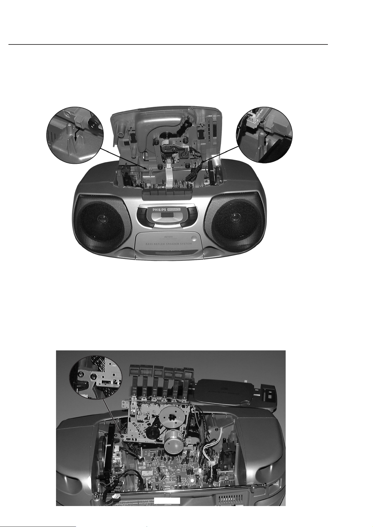
SERVICE HINTS
General Service position
picture 12
For repairs on: CD failures
Rec/Pb-amplifier
Power-amplifier
Power supply
Tuner Board
Service position Tape Transport
picture 13
For repairs on the Tape Transport or for
adjustment of the tape speed:
• Dismantle tape transport as described in
chapter 3-3.
• Fix tape transport on cabinet with one
screw as shown in picture 13.
• Connect cables on Combi Board again.
• Remove casstte door as described in chapter 3-1.
• Insert testcassette SBC420 (4822 397 30071)
directly into cassette compartment and play
10kHz part.
• Adjust right hand screw for max. output and
left channel = right channel.
3-6
CS 49 115
SERVICE HINTS
Alignment of AZIMUTH
picture 14
Details wire routing of mains transformer
picture 15
Wire routing has to be carried out as shown in picture
15 in order to:
•f
ulfil safety requirements and
• obtain tight speaker boxes
3-7
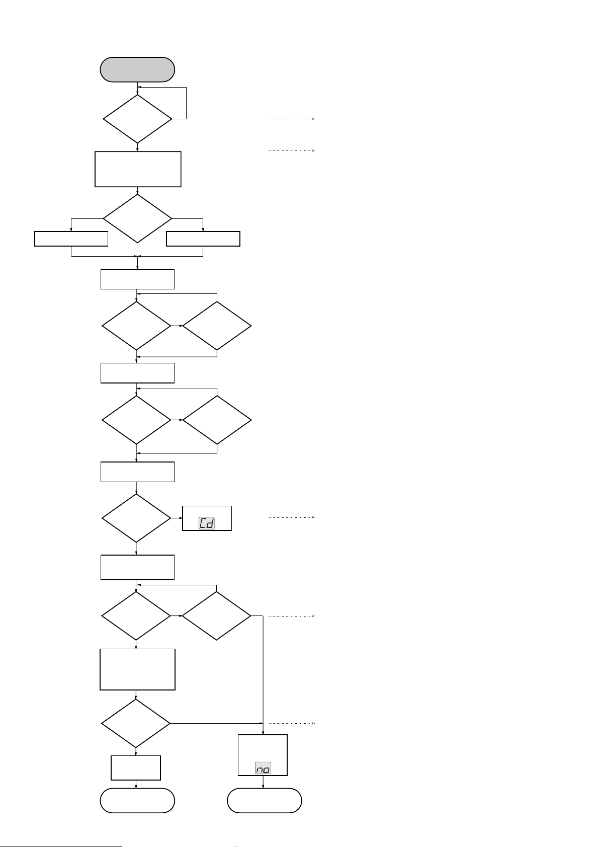
CS 49 116
N
Y
N
N
N
N
N
Y
CD switched on
(mode switch)
+A(CD)
supplied to
CD part?
Decoder delivers CLOCK -
frequ. 4.23MHz to µP.
µP-
RESET
line → high
µP init. Decoder 7801.
inner switch
closed?
4s time-out over?
0,2s time-out over?
inner switch open?
Laser on
Disc motor 100ms on
FOCUS search
on
focus found? 3s time-out over?
N
startup proc.
stopped,
display shows
µP initializes Decoder
and Servo IC:
-start turntable
-adj. track bal. and gain
-read subcode (TOC)
TOC
found?
display shows
max. trackno.
Y
Y
Y Y
N
Y Y
Remark: To check focus servo, slide servo, track servo and turntable
use service test program
- Battery empty?
- check +A,
- mode switch o.k.?
check: - Motor control pin 27 of Decoder 7801 and
Disc Motor driver 7805
- HF Signal by using service testprogram
check: - Laser light on ?
Check pin 38 of 7803 and
LASER CONTROL
circuit
- Focus Servo
HIGHLOW
Level on
pin23
(CD-RESET)
after 100µs?
Init. 7801 for ext. DAC Init. 7801 for int. DAC
BEGIN
µP moves slide inside
(4s time-out starts)
µP moves slide outside
(0,2s time-out starts)
STOP MODE STARTUP FAILED
CDstartup EVA, 080997
slide off
N
Y
check: - door switch
Door closed?
Display shows
check: - +A(CD), +B(CD), +LASER, +M,
- time constant of reset circuit
- Pin 32 of µP 7800 HIGH ?
- Pin 30 of µP 7800, if 4.23 MHz o.k.
CD STARTUP PROCEDURE

3-8
CS 49 117
SERVO PROCESSOR M62475FP
Pin Name Direction Description
1-3 A, B, C Diode array → Servo processor Current input ( central photo diode signal input )
4-5 E, F Diode array → Servo processor Current input ( satellite photo diode signal input )
6 SGT Servo processor → Track error ampl. input Signal generator output to track servo, sends 1700Hz for adjustment procedure
7 TE - - Inverting input of track error amplifier
8 TEGain - Gain control pin of track error amplifier
9 TG1 - Track Gain 1 - switch: controls the gain of the track servo amplifier
10 TE out - Track Error amplifier output
11 TC/Shock - Track Cross/Shock detector input
12 TS + - Non inverting input of track servo amplifier
13 TG2 not connected Track Gain 2 - switch: controls the gain of the track servo amplifier
14 TS - - Inverting input of track servo amplifier
15 TS out Servo processor → Servo driver Output of track servo amplifier
16 SS + - Non inverting input of slide servo amplifier
17 SS - - Inverting input of slide servo amplifier
18 Slide out Servo processor → Motor driver Output of slide servo amplifier
19 DET.FILTER - Pin for connection of DETection FILter capacitor of
ADJUST LOGIC
20 BIAS Servo processor → external electronic Reference Voltage output Vcc/2 of internal BIAS-generator
21 GND - Ground connection pin ( negative supply )
22 MLA/DIS µP → Servo processor Serial interface Microprocessor LAtch control / DIScharge control for adjustment
23 JP1/SG µP → Servo processor Serial interface Jump control line / Signal Generator input line for adjustment
24 MCK µP → Servo processor Serial interface Clock input line
25 MSD µP → Servo processor Serial interface Data input line
26 D
out
Servo processor → µP Serial interface Data output line
27 C
LPF
- Pin for connection of Low Pass Filter capacitor for
ADJUST LOGIC
28 I
REF
- Reference current input
29 V
CC
- Positive supply connection pin ( 4V - 5.5V )
30 FS
OUT
Servo processor → Servo driver Output of focus servo amplifier
31 FS - - Inverting input of focus servo amplifier
32 FEGain - Gain control pin of focus error amplifier
33 FE - - Inverting input of focus error amplifier
34 SGF Servo processor → Focus error ampl. input Signal generator output to focus servo, sends 1300Hz for adjust. procedure
35 C
FSR
- Charge capacitor for Focus Search triangle-generator
36 ALPC + - Non inverting input of Automatic Laser Power Control amplifier
37 ALPC - - Inverting input of Automatic Laser Power Control amplifier
38 ALPC
OUT
Servo processor → Laser driver Output of Automatic Laser Power Control amplifier
39 MRC - Connection pin for capacitor of Mirror detector
40 HF Servo processor → Decoder Output of HF amplifier
41 HFI - Inverting input of HF amplifier
42 ABC - Sum output of amplified A, B and C input ( central photo diode signal input )
to external ac-coupling capacitor
SIGNAL PROCESSOR M65824FP
Pin Name Direction Description
1 Anal. V
SS
- Analog system ground
2 ADJCLK not connected Clock output for servo adjustment; f=88.2kHz
3 LOCK not connected Lock monitor / low disc rotation output
4 CKSEL - System clock selection. Low=8.4672MHz, high=16.9344MHz
5 RESET µP → Signal processor System reset ( low level = active )
6 C423 Signal processor → µP 4.2336MHz clock output
7 C846 not connected 8.4672MHz clock output
8 XI X-Tal → Signal processor Crystal oscillator input
9 DVSS - Digital system ground
10 XO Signal processor → X-Tal Crystal oscillator output
11 TEST - Normal / Test selection input. Testmode = high
12 SBCO not connected Subcode serial output
13 SCCK - Shift clock input for subcode data read
14 SYCLK not connected Frame lock status output. Lock = high
15 EFFK not connected EFM frame clock output. Duty = 50%
16 KILLB not connected Digital silence mute output. Digital zero = low
17 EST1 not connected Error monitor output 1
18 EST2 not connected Error monitor output 2
19 HF Servo processor → Signal processor HF signal input
20 TLC - Slice level control signal output
21 LPF - PLL loop filter
22 Dig.V
DD
- Digital interface power supply
23 DSPS - Digital system power supply
24 SBQS not connected Interrupt signal to read out subcode Q data. Read = low
25 CRCF not connected Subcode Q-channel Cyclic Redundance Check Flag output. CRC o.k.=high level
26 SCAND not connected Subcode sync signal detection. Sync = high
27 PWM Signal processor → Motor driver Disc motor driving ( Pulse Width Modulation ) output
28 DVDD2 - Digital interface power supply 2
29 DVSS2 - Digital system ground2
30 MCK µP → Signal processor µP interface shift Clock input
31 MSD µP ↔ Signal processor µP interface Serial Data I/O line
32 MLAB µP → Signal processor µP interface Latch clock input ( internal 22k pull up resistor )
33 EXP1 →Signal processor Versatile input pin ( internal 4.7k pull up resistor )
34 EXP2 →Signal processor Versatile input pin ( internal 4.7k pull up resistor )
35 CGREF → Signal processor Charge-pump for LPF reference current input
36 AMPREF not connected Op-amp for LPF reference voltage setting
37 LOUT/DO Signal processor → Audio signal output (left channel) / Ext. DAC mode: Audio serial data output
38 LNEG not connected Charge pump output (left channel) / Ext. DAC mode: Wordclock output
39 ROUT/DSCK Signal processor → Audio signal output (right channel) / Ext. DAC mode: Data shift clock output
40 RNEG/LRCK Signal processor → Charge pump output (right channel) / Ext. DAC mode: L/R clock output
41 IREF - Current reference
42 Anal. V
DD
- Analog System power supply
Pin-descriptions of CD ICs
 Loading...