

查询AU211供应商
INTEGRATED CIRCUITS
AU211/LM111/211/311/311B
Voltage comparator
Product data
Supersedes data of 2001 Aug 03
2003 Sep 30
Philips Semiconductors Product data
AU21 1/LM11 1/211/31 1/311BVoltage comparator
DESCRIPTION
The LM111 series are voltage comparators that have input currents
approximately a hundred times lower than devices like the µA710.
They are designed to operate over a wider range of supply voltages;
from standard ±15 V op amp supplies down to a single 3 V supply.
Their output is compatible with RTL, DTL, and TTL as well as MOS
circuits. Further, they can drive lamps or relays, switching voltages
up to 50 V at currents as high as 50mA.
Both the inputs and the outputs of the LM111 series can be isolated
from system ground, and the output can drive loads referred to
ground, the positive supply, or the negative supply. Offset balancing
and strobe capability are provided and outputs can be wire-ORed.
Although slower than the µA710 (200 ns response time versus 40 ns),
the devices are also much less prone to spurious oscillations. The
LM111 series has the same pin configuration as the µA710 series.
FEA TURES
•Operates from single 3 V supply (LM311B)
•Maximum input bias current: 150 nA (LM311: 250 nA)
•Maximum offset current: 20 nA (LM311: 50 nA)
•Differential input voltage range: ±30 V
•Power consumption: 135 mW at ±15 V
•High sensitivity: 200 V/mV
•Zero crossing detector
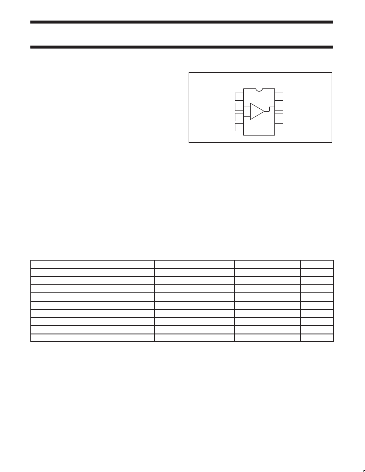
PIN CONFIGURATION
D, N Packages
1
GND
2
INPUT
INPUT
V–
Figure 1. Pin Configuration
+
–
3
45
APPLICATIONS
•Precision squarer
•Positive/negative peak detector
•Low voltage adjustable reference supply
•Switching power amplifier
8
V+
7
OUTPUT
6
BAL/STROBE
BALANCE
SL00062
ORDERING INFORMATION
DESCRIPTION TEMPERATURE RANGE ORDER CODE DWG #
8-Pin Plastic Small Outline Package (SO) –40 °C to +125 °C AU211D SOT96-1
8-Pin Plastic Small Outline Package (SO) –55 °C to +125 °C LM111D SOT96-1
8-Pin Plastic Dual In-Line Package (DIP) –55 °C to +125 °C LM111N SOT97-1
8-Pin Plastic Small Outline Package (SO) –25 °C to +85 °C LM211D SOT96-1
8-Pin Plastic Dual In-Line Package (DIP) –25 °C to +85 °C LM211N SOT97-1
8-Pin Plastic Small Outline Package (SO) 0 °C to +70 °C LM311D SOT96-1
8-Pin Plastic Dual In-Line Package (DIP) 0 °C to +70 °C LM311N SOT97-1
8-Pin Plastic Small Outline Package (SO) 0 °C to +70 °C LM311BD SOT96-1
8-Pin Plastic Dual In-Line Package (DIP) 0 °C to +70 °C LM311BN SOT97-1
2003 Sep 30
2

Philips Semiconductors Product data
2
AU211/LM1 11/211/311/311BVoltage comparator
EQUIVALENT SCHEMATIC
BALANCE/
STROBE
BALANCE
V+
INPUTS
R3
300
Q1
Q5
R1
1.3 kΩ
D1
5 VD25 V
R4
300
Q2
R2
1.3 kΩ
R8
750
Q8
R5
70
R6
1.2 kΩR71.2 kΩ
Q3
Q4
Q23
R19
250
Q7
Q8
Q2
R18
200
Q9
Q22
Q10
R17
60
R14
2 kΩ
Figure 2. Equivalent Schematic
Q11
Q19
R9
600
R15
400
R15
450
Q17
Q18
Q20
R10
4 kΩ
Q18
Q13
Q14
V–
Q12
R11
130
R12
600
Q15
R13
4
OUTPUT
SL00063
ABSOLUTE MAXIMUM RATINGS
SYMBOL PARAMETER RATING UNIT
V
S
V
IN
P
D MAX
I Output short-circuit duration 10 sec
T
amb
T
stg
T
sld
NOTES:
1. This rating applies for ±15 V supplies. The positive input voltage limit is 30 V above the negative supply. The negative input voltage limit is
equal to the negative supply voltage or 30 V below the positive supply, whichever is less.
2. Derate above 25 °C, at the following rates:
Total supply voltage 36 V
Output to negative supply voltage
LM111/LM211 50 V
LM311/LM311B 40 V
Ground to negative supply voltage 30 V
Differential input voltage ±30 V
Input voltage
Maximum power dissipation, T
1
= 25 °C (still-air)
amb
N package 1190 mW
±15 V
D package 780 mW
Operating ambient temperature range
AU211 –40 to +125 °C
LM111 –55 to +125 °C
LM211 –25 to +85 °C
LM311/LM311B 0 to +70 °C
Storage temperature range –65 to +150 °C
Lead soldering temperature (10 sec max) 230 °C
N package at 9.5 mW/°C
D package at 6.2 m/W°C
2003 Sep 30
3
 Loading...