


APPLI C ATION NOT E
PCA82C250 / 251
CAN Transceiver
AN96116

Philips Semiconduct or s
PCA82C250 / 251 CAN Transceiver
Appl ica tio n Note
AN96116
Abstract
The PCA82C250 and PCA82C251 are advanced transceiver products for use in automotive and general industrial applications with transf er rates up to 1 Mbit/s. They support the differential bus signal repre sentat ion being
described in the international standard for in-vehicle CAN high-speed app licat ions (ISO 11898). Controller Area
Network (CAN) is a serial bus protocol being primarily intended for transmission of control related data between a
number of bus nodes.
This application note provides inform at ion how to use the above-men tion ed transceiver product s and discusses
several topics of interest like slope control mode, stand-by mode, bus length and maximum number of bus nodes
per network.
Philips Electronics N.V. 1996
All rights are reserved. Reproduction in whole or in part is prohi bited without the prior written consent of the copyright owner.
The information presented in this document does not form part of any quotation or contract, is believed to be
accurate and reliable and may be changed without notice. No liability will be accepted by the publisher for any
consequence of its use. Publication thereof does not convey nor imply any license under patent - or other industrial or intellectual property rights.
2

Philips Semiconduct or s
PCA82C250 / 251 CAN Transceiver Application Note
AN96116
APPLI C ATION NOT E
PCA82C250 / 251
CAN Transceiver
AN96116
Author(s):
Harald Eisele, Egon Jöhnk
Product Conce pt & Application Laboratory Hamburg,
Germany
Keywords
Transceiver, ISO 11898, Physical Layer,
Slope-Control, Bus Length, PCA82C250, PCA82C251,
Controller Area Network (CAN)
Supersedes Data of 1996 Apri l 17 (AN96001)
Date: 1996 October 23
3

Philips Semiconduct or s
PCA82C250 / 251 CAN Transceiver
Appl ica tio n Note
AN96116
Summary
This report is intended to provide basic technical information for the implement ation of the Physical Medium
Attachment in a CAN network according to the ISO 11898 standard, using the transceiver products PCA82C250
and PCA82C251 from Ph ilip s Sem iconductors. These products support bit rate s up to 1 Mbit/s over a two-wire
differential bus line, which is the transmission medium being specified by the ISO 11898 standard.
The report provides typical application circuit diagrams with and without electrical isolation and discusses several
topics in more detail like slope control mode, stand-by mode, maximum bus length and maximum number of bus
nodes per network.
4

Philips Semiconduct or s
PCA82C250 / 251 CAN Transceiver
Appl ica tio n Note
AN96116
CONTENTS
1. INTRODUCTION . . . . . . . . . . . . . . . . . . . . . . . . . . . . . . . . . . . . . . . . . . . . . . . 7
2. APPLICATION OF THE PCA8 2C250 AND PC A82C251 . . . . . . . . . . . . . . . . . . . . . . . . . . 8
2.1 Application Examples. . . . . . . . . . . . . . . . . . . . . . . . . . . . . . . . . . . . . . . . . 9
2.2 Reference Voltage Out put . . . . . . . . . . . . . . . . . . . . . . . . . . . . . . . . . . . . . 11
3. OPERA TION MO DE S . . . . . . . . . . . . . . . . . . . . . . . . . . . . . . . . . . . . . . . . . . . 12
3.1 High-Speed Mode . . . . . . . . . . . . . . . . . . . . . . . . . . . . . . . . . . . . . . . . . 1 2
3.2 Slope Control Mode . . . . . . . . . . . . . . . . . . . . . . . . . . . . . . . . . . . . . . . . 12
3.3 Stand-by Mode . . . . . . . . . . . . . . . . . . . . . . . . . . . . . . . . . . . . . . . . . . . 13
4. SLOPE CONTRO L FUNCTION . . . . . . . . . . . . . . . . . . . . . . . . . . . . . . . . . . . . . . 14
4.1 Slew Rate Calculation . . . . . . . . . . . . . . . . . . . . . . . . . . . . . . . . . . . . . . . 14
4.2 Bus Length in Slope Control Mode . . . . . . . . . . . . . . . . . . . . . . . . . . . . . . . . . 16
5. MAX I MUM BUS L INE LENGT H . . . . . . . . . . . . . . . . . . . . . . . . . . . . . . . . . . . . . . 17
5.1 Impact of the Bus Cable Resistance . . . . . . . . . . . . . . . . . . . . . . . . . . . . . . . . 1 7
5.2 Maximum Number of Nodes . . . . . . . . . . . . . . . . . . . . . . . . . . . . . . . . . . . . 19
5.3 E x a mp l e s. . . . . . . . . . . . . . . . . . . . . . . . . . . . . . . . . . . . . . . . . . . . . . 20
6. BUS TERMIN ATION AND TOP OL OG Y ASPEC TS . . . . . . . . . . . . . . . . . . . . . . . . . . . . 22
6.1 Split Termination Conce pt . . . . . . . . . . . . . . . . . . . . . . . . . . . . . . . . . . . . . 2 2
6.2 Multiple Termination Concept . . . . . . . . . . . . . . . . . . . . . . . . . . . . . . . . . . . 22
6.3 Single Termination Concept . . . . . . . . . . . . . . . . . . . . . . . . . . . . . . . . . . . . 23
6.4 Termination Mismatch . . . . . . . . . . . . . . . . . . . . . . . . . . . . . . . . . . . . . . . 23
6.5 Unterminat ed Cable Drop Lengt h . . . . . . . . . . . . . . . . . . . . . . . . . . . . . . . . . 2 4
7. CONCLUSION . . . . . . . . . . . . . . . . . . . . . . . . . . . . . . . . . . . . . . . . . . . . . . . 25
8. LIST OF REFERENCES . . . . . . . . . . . . . . . . . . . . . . . . . . . . . . . . . . . . . . . . . . 25
APPENDIX 1 ABBREVIATIONS AND DEFINITIONS . . . . . . . . . . . . . . . . . . . . . . . . . . . . 26
APPENDIX 2 CALCULATION OF THE VOLTAGE AT THE INPUT OF A NODE . . . . . . . . . . . . . . 27
APPENDIX 3 CALCULATION OF THE MAXIMUM BUS L INE LENGT H . . . . . . . . . . . . . . . . . . 28
5

Philips Semiconduct or s
PCA82C250 / 251 CAN Transceiver
(page has been left blank intentionally)
Appl ica tio n Note
AN96116
6

Philips Semiconduct or s
PCA82C250 / 251 CAN Transceiver
Appl ica tio n Note
AN96116
1. INTRODUCTION
ISO 118 98 [3] is the internati onal stan dard for in-vehicle high-speed comm uni ca tion using the Controller A rea
Network (CAN) bus protocol. The scope of this standard essentially is to specify the so-called data link layer and
physical layer of the communication link. The physical layer is subdivided into three sublayers as shown in Fig. 1.
These are
• Physical Signalling bit coding, timing and synchronization
• Physical Medium Attachment driver and receiver characteristics
• Medium Dependent I nterface bus connector
This report focuses on the implementation of the Physical Medium Attachment sublayer using the transceivers
PCA82C250 [1] and PCA82C251 [2] from Philips Semiconductors. The implementation of the Physical Signalling
sublayer and the Data Link Layer is typically performed by integrated protocol controlle r products, like the
PCx82C200 from Ph ilip s Semiconduct or s. Connection to the transm ission medium is provided via the Medium
Dependent Interface i.e. a connector used to attach bus nodes to the bus line.
SPECIFICATION IMPLEMENTATIONOSI-LAYER
TO BE SPECIFIED BY
THE SYSTEM DESIGNER
DATA LINK
CAN-PROTOCOL
SPECIFICATION
SCOPE OF ISO 11898
Note: OSI = Open Systems Interconnection (see ISO 7498)
LAYER
PHYSICAL
LAYER
Fig. 1 Layered architecture of CAN
APPLICATION LAYER
MEDIUM ACCESS CONTROL
PHYSICAL MEDIUM ATTACHMENT
MEDIUM DEPENDENT INTERFACE
TRANSMISSION MEDIUM
LOGICAL LINK CONTROL
CAN-CONTROLLER
e.g.
PCx82C200
PHYSICAL SIGNALLING
CAN-TRANSCEIVER
PCA82C250/251
JK512191.GWM
7

Philips Semiconduct or s
EI203030
CAN_H
CAN_L
5V
3.5V
1.5V
0V
2.5V
Recessive Dominant Recessive
Time
Voltage
PCA82C250 / 251 CAN Transceiver
Appl ica tio n Note
AN96116
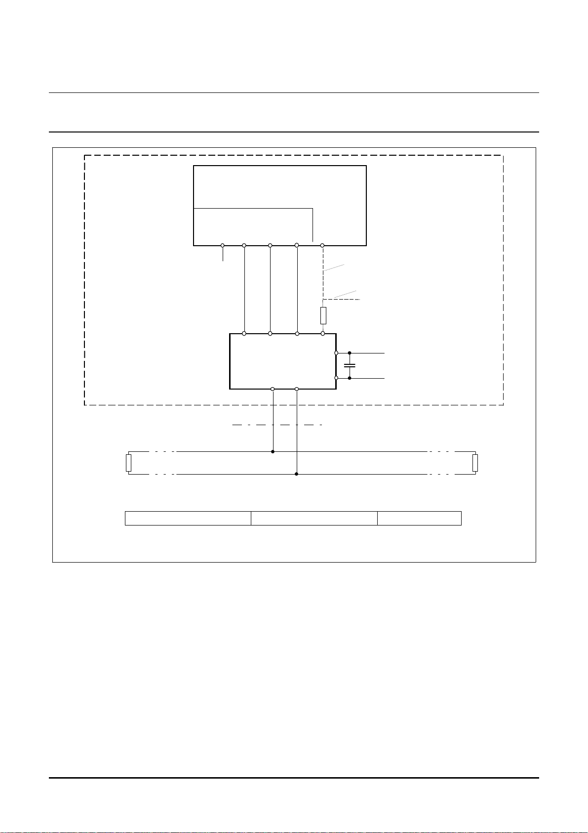
2. APPLICATION OF THE PCA82C250 AND PCA82C251
The PCA82C250/251 transceiver products basically provide interfacing between a protocol controller and a physical transmission line. They are designed to transmit data with a bit rate of up to 1 Mbit/s over a two-wire differential voltage bus line as described in the ISO 11898 standard. Their general features are listed in the data sheets
(see [1] and [2]).
Both devices are designed for the use in CAN bus systems with a nomin al supply volta ge of 12 V (PCA82C250)
and 24 V (P CA82C251) respecti ve ly. The y are function ally ident ical and can be used in automot ive and general
industrial applications accordi ng to the relevant standards e.g. the ISO 11898 stand ard [3] and the DeviceNet
Specification [5]. Both the PCA82 C250 and the PCA82C251 can commun icate to one another in one network.
Moreover they are pin- & function-compat ible i.e. they can be used with identical printed circuit boards.
Some main differences between both products are listed in Tabl e 1.
Table 1 M ain differen ces between PCA82C250 and PCA82C251
PCA82C250 PCA82C251
Nominal system supply volta ge 12 V 12V and/or 24 V
Maximum bus term inal D C volt a ge
(0 V < V
< 5.5 V)
CC
−−8V < V
CANL,H
< +18 V −−40 V < V
CANL,H
TM
< +40 V
Maximum transient bus terminal voltage
(ISO 7637)
Minimum transceiver supply voltage f or extended fan
out applications (R
= 45 Ω)
L
−−150 V < V
V
< +100 V −200 V < Vtr < +200 V
tr
> 4.9 V VCC > 4.5 V
CC
For general industrial applications the PCA82C251 is recommended to be employed as to e.g. its higher breakdown voltage and its capability to drive loads down to 45 Ω over the whole supply vo lta ge range. A lso the
PCA82C251 draw s less supply current in the recessive state and provides an enhanced bus output beh aviour in
power-fail situati ons.
Fig. 2 Nominal bus levels according to ISO 1 1898
8
Philips Semiconduct or s
PCA82C250 / 251 CAN Transceiver
e.g. PCx82C200
CAN - Contoller
CTX0
CTX1
/ TX1
CRX0
/ TX0
/ RX0
TxD RxD VREF Rs
PCA 82C250/251
CAN Transceiver
CANH CANL
uC
CRX1
/ RX1
Px,y
either connection to an output port pin,
if standby mode shall be possible
or
connection to ground
0V
R
ext
V
CC
GND
+5V
100n
0V
Appl ica tio n Note
AN96116
JK512151.GWM
ISO 11898 Standard
CAN_H
124
Programming of the Output Control Register (example)
Output Control TX0 push-pull, dominant = low e.g. 1A
Fig. 3 Application example of the PCA82C250/251 transceivers
CAN Bus Line
CAN_L
hex
124
2.1 Application Examples
A typical application of the PCA82C250/251 transceiver is shown in Fig. 3. A protocol controller is connected to
the transceiver via a serial data output line (TX) and a serial data input line (RX). The transceiver is attached to
the bus line via its two bus terminals CANH and CANL , which provide differential receive and transmit capability.
The input Rs is used for mode control purpose. The reference voltage output V
0.5 × V
nominal. Both transcei ve r products are powe red wi th a nom inal suppl y voltage of +5 V.
CC
The protocol controller outp uts a serial transm it data stream to the TxD input of the trans ceiver. A n internal pullup function sets the TxD input to logic HIGH i.e. the bus out put driver is passive by default . In this so-called
recessive state (see Fig. 2) the CANH and CANL inputs are biased to a voltage level of 2.5 V nominal via
receiver input networks with an internal impedance of 17 kΩ typical. Otherwi se if a logic LOW-le ve l is applied to
TxD, this activates the bus output stage, t hus generat ing a so-called dom inant signal level on the bus lin e (see
Fig. 2). The output driver consists of a source and a sink output stage. CANH is attached to the source output
and CANL to the sink output stage. The nom inal volt age in the domin ant sta te is 3.5 V for the CAN_H line and
1.5 V for the CAN_L lin e.
provides an output voltage of
REF
9

Philips Semiconduct or s
PCA82C250 / 251 CAN Transceiver
CAN - Contoller
CTX0
CTX1
/ TX0
/ TX1
360
Isolation
+5V
6N137
360
+5V
+5V
100n
0V
TxD RxD VREF Rs
PCA 82C250/251
CAN Transceiver
CRX0
/ RX0
360
+5V
360
n.c.
CANH CANL
CRX1
/ RX1
100n
6N137
V
CC
GND
e.g. PCx82C200
4.3k6.2k
0V
either connection to
R
ext
high-active reset signal
+5V
100n
0V
or connection to ground
Appl ica tio n Note
AN96116
RST
5V
Regulator
JK512152.GWM
ISO 11898 Standard
CAN_H
124
Programming of the Output Control Register (example)
Output Control TX0 push-pull, dominant = low e.g. 1A
Fig. 4 Application example for an interface with galvanic isolation using optocouplers
Note: If high bit rates shall be used, e.g. 500 kbit/s or above, then high-speed optocouplers should be considered with a delay of less than 40ns, e.g. HCPL-7101.
CAN Bus Line
CAN_L
124
hex
The bus line is in recessive state if no bus node transmits a dominant bit, i.e. all TxD input s in the network are
logic HIGH. Otherwi se if one or m ultiple bus nodes transmit a domi nant bit, i.e. at least one TxD input is logic
LOW, then the bus line enters the dominant state thus overriding the recessive state (wired-AND ch aracteristic).
10

Philips Semiconduct or s
PCA82C250 / 251 CAN Transceiver
Appl ica tio n Note
AN96116
The receiver comparator converts the differential bus signal to a logic level signal which is output at RxD. The
serial receive data stream is provided to the bus protocol controller for decoding. The receiver comparator is
always active i.e. it monitors the bus while the bus node is transmitting a message. This is required e.g. for safety
reasons and to support the non-destructive bit by bit contention scheme of CAN. Some controller products provide an analog receive interface (RX0, RX1). In that case RX0 usually needs to be connected to the RxD output
and RX1 needs to be biased to an appropriate voltage level. This can be done e.g. by using the V
Fig. 3) or by using a resistive voltage divider (see Fig. 4).
In Fig. 3 the transceiver is directly connected to the protocol controller and its application circuitry. In cases where
galvanic isolation is desired, optocouplers can be placed e.g. between the transceiver and the protocol controller
as shown in Fig. 4. When using optocouplers one has to pay attention to choose the right default state when the
circuitry at the protocol controller side of the isolation is not powered. In such a case the optocoupler being
attached to TxD will be “dark” i.e. LED switched off. When this optocoupler is off/dark, then a logic HIGH-level
has to be output to the TxD input of the transceiver for fail-safe purpose. Also if using optocouplers one may consider to attach the Rs mode control input to an active-high reset signal, e.g. to disable the transceiver when the
local transceiver supply voltage is not OK e.g. during ramp-up and -down.
However using optocouplers generally increase s the so-called loop delay of a bus node, if placed between the
transceiver and the protocol controller. The signal has to pass these devices twice per node, i.e. transmit and
receive path, which effectively decreases the maximum achievable bus length at a given bit rate. This fact has to
be considered when calculating the maximum achievabl e bus length due to propagation del ay s in a CAN network. For more details please refer e.g . to [4].
output (see
REF
2.2 Reference Voltage Output
The PCA82C250/251 provides a reference voltage output V
inputs of a CAN protocol controller´s differential inpu t comparator as shown in Fig. 3. In other cases a reference
voltage may be generated locally at the protocol co ntrol ler input as shown e.g. in Fig. 4. Which solution is appropriate in a system depends on the application and the bus input struct ure of the protocol controlle r product.
, which may be used e.g. to bias one of the
REF
11

Philips Semiconduct or s
PCA82C250 / 251 CAN Transceiver
Appl ica tio n Note
AN96116
3. OPERATION MODES
The PCA82C250 and PCA82C251 provide three different operation m odes. Mode control is being provided
through the Rs control inp ut.
The first mode is the high-speed mode supporting m aximum bus speed and/ or lengt h.
The second mode is the so-called slope control mode which should be considered if unshielded bus wires shall
be used. In this mode the output slew rate can be decreased intent ion ally, e.g. to reduce electromagn eti c emission.
The third mode is the stand-by mode being of interest especially in battery powered appl icati ons, when the system power consumption needs to be very low. System reactivation is performed through transmission of a message. Fig. 3 gives an example for switching the transceiver between stand-by mode and normal operating mode.
• Px,y = HIGH: the PCA82 C 250/251 is switched to stand-by mode (V
• Px,y = LOW: the PCA82C2 50/2 51 is switched to normal operating mode, which is either high-spe ed mode
or slope control mode, depending essentially upon the resistance connect ed to Rs.
Usually the following resistance values for the slope-control resistor R
• 0 Ω < R
• 16.5 kΩ <R
< 1.8 kΩ high-speed m ode (VRs < 0.3 × VCC)
ext
< 140 kΩ slope control mode (10 µA < - IRs < 200 µA)
ext
In the following these three operation modes shall be discussed in more detail .
> 0.75 × VCC)
Rs
are suitable:
ext
3.1 High-Speed Mode
This mode is suitable to achieve a maximum bit rate and/or bus length. The high-speed mode is commonly
employed in general industrial application s such as the CAN based system DeviceNet
output signals are switched as fast as pos sible and therefore a shield ed bus cable usually would be appropria te
to prevent a possible disturbance of e.g. a car radio by the bus signal.
The high-speed mode is selected with V
<0.3×VCC. This can be achieved with a direct connection of the Rs
Rs
control input to an output port of a microcontroller or ground potential or an active-high reset signal (see Fig. 3
and Fig. 4).
In high-speed mode the transceive rs provide an effect ive loop delay of as low as 145 ns max. (155 ns for
>85°C). With view to the CAN bit timing requirements, the effective loop delay is the maximum of the dom-
T
amb
inant edge loop delay and the average value of dominant and recessive edge loop delay.
t
loop.eff
max 0.5 t
{,}=
+()× t
onRxDtoffRxD
onRxD
TM
. In this mode the bus
3.2 Slope Control Mode
In several applications the use of an unshielded bus cable will be desirable e.g. for system cost reasons. However using an unshielded cable implies additional requirements to be met by the transceiver product e.g. with
view to electromagnetic compat ibi lity (EMC ). Using the PCA 82C250/ 251 the slew rate of the bus signal can be
decreased intentionally, which is recomm ended if an unshielded bus cable shall be used. The slew rate can be
set via a series resistance value R
requirements a decreased slew rate implies an increase of the bus node loop delay and thus a lower bus length
at a given bit rate or alternatively a lower bit rate at a given bus length. In slope control mode the bus output slew
rate is basically proportional to the current flow out of pin Rs in the range of 10 µ A < - I
sheets [1], [2]). If the Rs output current is in that range, then a voltage of approximately 0.5 × V
at the pin Rs. The transceiver is set to slope control mode when an appropria te resistance value is applied
between the Rs pin and ground potential. As a rule of thumb the resistance value should be in the range of
16.5 k Ω <R
< 140 kΩ to meet the above-mentioned range for the Rs output current.
ext
being connected to the control pin Rs. With respect to the CAN bit timing
ext
< 200 µA (see data
Rs
will be output
CC
12

Philips Semiconduct or s
PCA82C250 / 251 CAN Transceiver
Appl ica tio n Note
AN96116
The suitable range for R
10 µA<-I
<200µA and 0.4 × VCC<VRs< 0.6 × VCC.
Rs
The minimum and maxim um values for R
tion of the symbols see APPENDIX 1).
0.6 V
ext
R
------------------------------ -
ext
R
If the slope control resistor R
between the Rs output current and the bus signal slew rate is discussed in chapter 4.1.
3.3 Stand-by Mode
This mode is to be used when the power consumption needs to be minimized e. g. tempora rily. Th e stand-by
mode is selected with V
Using the stand-by mode, the system power consumption can be reduced drastically. This mode is primarily
intended for battery powered applications for example when a vehicle is parked. To enter stand-by mode a logic
HIGH-level has to be applied to the transceiver´s control input Rs. This can be done either by direct connection of
an output port pin to Rs or via any suitable slope control resist or R
and the receiver input bias network are switched off to reduce power consumption. The reference voltage output
and a basic receive function will remain active and work wit h very low power consumption . This allows to reactivate the system via the bus line by transmission of a message. Upon detection of a dominant bus condit ion of at
least 3 µs length, the transceiver will provide a wake-up interrupt signal to the protocol controller via its RxD output. Upon detection of a falling edge on RxD the cont roller should set the Rs pin to logic LOW-level in order to
switch the transceiver back to normal transmission mode. As the receiver is slower in stand-by mode, it essentially depends on the delay time of the logic (falling edge on Rs) when the transceiver is back to normal reception
speed. At high bus speeds the transceiver may not be able to correctly receive messages in stand-by mode i.e.
while the Rs pin is still HIGH.
An alternative applicatio n is to connect the Rs input to an active-high reset signal. This can be done for example
with view to the case of the transceiver and the protocol controller being supplied by different supply sources,
e.g. if optocouplers are used (see Fig. 4).
can be calculated using the limits for slope control mode
ext
can be calculated with the following two relations (for the explana-
ext
CC.max
I
Rs.max
0.4V
---------------------------------- ------------------------
> 0.75 × VCC.
Rs
0.6 V
CC.max
------------------------------ -=>
200µA
CC.minVOL.max
ext
–
I
Rs.min
is connected to ground, then the value V
0.4V
CC.minVOL.max
------------------------------------- ----------------------
=<
–
10µ A
. In stand-by mode the transmitter functio n
ext
OL.max
(1)
(2)
is zero volts. The relation
13

Philips Semiconduct or s
I
Rs
V
Rs
R
ext
----------- k
SE
SR×==
k
SE
0.5V
CC
R
ext
SR×
------------------------- -
2.5V
47kΩ 7
V
µs
------
×
------------------------------ - 7. 6 10
3–
µ s
k Ω
-------
×== =
PCA82C250 / 251 CAN Transceiver
Appl ica tio n Note
AN96116
4. SLOPE CONTROL FUNCTION
4.1 Slew Rate Calculation
As mentioned above, the slew rate (SR) of the bus output signal is proportional to the current flow (IRs) out of the
pin Rs. As the current is primarily determined by the slope- control resistance value R
achieved by applying a respective resistance. Note that there is a difference between the single-ended slew rate,
which applies to each bus voltage individually and the differential signal slew rate, which applies to the differential
voltage between CANH and CANL. Fig. 5 gives typical single-ended slew rate values as a function of the slopecontrol resistance value (see equat ion (4)).
single ended
slew rate for
CANH,CAN L
20
[V/µs]
15
, a certain slew rate is
ext
10
5
10 50 100
Fig. 5 Diagram: Slew rate versus slope control resistance value
These values are derived using the typical slew rate value given in the data sheets [1] and [2]:
SR (CANH or CANL) = 7 V/µs typ. at R
In slope-control mode the Rs-volt age is V
= 0.5 × VCC typ.
Rs
As with k
=47kΩ (connecte d betwee n input Rs and 0 V, see Fig. 3)
ext
: single-ended slew rate constant
SE
140
R
ext
[kΩ]
the slew rate constant (single-ended) can be calculated using above typical values.
(3)
14

Philips Semiconduct or s
SR
V
RsVOL
–
k
SERext
×
--------------------------- -
V
RsVOL
–
7.6 10
3–
µs
kΩ
-------
× R
ext
×
----------------------------------------------------- -==
PCA82C250 / 251 CAN Transceiver
Appl ica tio n Note
AN96116
Normally for slope control mode the resistor R
), provided either by a port output or a ground line. Thus the relation between the single-ended slew rate and
(V
OL
the resistance R
is given by the following equation:
ext
Example 1:
With R
= 24 kΩ and VOL = 0V the single-ended slew rate typically would be
ext
V
SR
–
RsVOL
--------------------------- -
×
k
SERext
0.5V
----------------------------------------------------- -
7.6 10
CC
µs
3–
-------× R
kΩ
×
Example 2:
To achieve a single-ended slew rate of 5 V/µs the typical slope-control resistance would be
V
–
R
ext
RsVOL
-------------------------- -
k
SE
S× R
0.5V
-------------------------------------------------- -
7.6 10
CC
µs
3–
-------× SR×
kΩ
is connected between the input Rs and and a logic LOW-level
ext
. (4)
0.5 5V×
-------------------------------------------------------- -
7.6 10
ext
0.5 5 V×
---------------------------------------------------- -
7.6 10
µs
3–
-------× 24kΩ×
kΩ
µs
3–
-------× 5
kΩ
------×
µ s
V
V
14
------== = =
µs
===> R
66 k Ω== = =
= 68 kΩ
ext
15

Philips Semiconduct or s
L
max
t
prop
2
------------ t
loop.efftloop.eff.oth
––
t
p
------------------------------------------------------------------------- -=
PCA82C250 / 251 CAN Transceiver
Appl ica tio n Note
AN96116
4.2 Bus Length in Slope Control Mode
In slope control mode the bus output slew rate is decreased intent ionally, which im plie s an increase of the bus
node loop delay. Due to the CAN bit timing requirement s, this is equivalent to a reduction of the maximum bus
line length at a given bit rate or reduction of the bit rate at a given bus length in a system compared to using the
high-speed mode.
The maximum achieva ble bus line leng th is given by (see also [4]):
(5)
With L
max
t
prop
t
loop.eff
t
loop.eff.oth
t
p
From equation (5) it is obvious, that the maximum bus line lengt h will increase, if the transceiver loop delay is
decreased. The loop delay of a transceiver, which is set to the high-speed mode, is smaller than the loop delay of
a transceiver, which is set to the slope cont rol mod e. Thus a higher bus line length can be achieved, if the transceiver is used in the high-speed mode, as a greater portion of the available propagation delay can be used for tolerating line delay.
: Maxim um achievable bus line leng th
: Maximum available two-way propagation delay (CAN bit timin g)
: Effect ive transceiver loop del ay
: Effect ive loop delay of other component s e.g. CAN control ler and optocou plers
: Specif ic bus line delay
This increase is given by the following equation:
∆L
max
t
loop.eff
----------------------------------------------------------------------------------------------------------------------------------------------
slope control mode() t
loop.eff
t
p
high speed mode()–
∆ t
loop.eff
---------------------- -==
t
p
(6)
In a CAN network the effective maximum delay of a transceiver (also valid for the delay of other devices) are calculated using the following equation
(See APPENDIX 1 for an explanation of used symbols and abbreviat ions):
t
loop.eff.max
max 0.5 t
{,}=
onRxDtoffRxD
+()× t
onRxD
(7)
Table 2 gives an indication of the difference between using high-speed mode and slope control mode - in terms
of maximum bus length. The values below refer to a specific propagation delay of t
= 5 ns/m on the bus cable.
p
Table 2 Difference of maximu m bus length
Effective loop del ay
Product slope-control mode2high-speed mode ∆ t
(upper limit at 125oC)
loop.eff
Difference between both
modes in terms of bus length
∆ L
max
1
PCA82C250 520 ns 155 ns 365 ns ~ 75 m
PCA82C251 550 ns 155 ns 395 ns ~ 80 m
1. At 5 ns/m specific propagation delay on the bus cable
2. Slope-control resistance R
= 47 kΩ
ext
16

Philips Semiconduct or s
PCA82C250 / 251 CAN Transceiver
Appl ica tio n Note
AN96116
5. MAXIMUM BUS LINE LENGTH
The maximum achieva ble bus line leng th in a CAN bus network is determined e ssenti ally by the followin g physical effects:
1. The loop delays of the connected bus nodes (CAN controller, transceiver etc.) and the delay of the bus line
2. The differences in bit time quantum length due to the relative oscilla tor tol erance betw een nodes
3. The signal amplitude drop due to the series resistance of the bus cable and the input resistance of bus
nodes
The effect 3. is discussed below.
The effects 1. and 2. are not discussed in this document (please refer e.g. to [4]). However as a rule of thumb the
following bus line length can be achieved with the PCA82C250 and PCA82C251 in high-speed mode and with
CAN bit timing parameters being optim ized fo r maximum propa gati on delay:
Table 3 Bit Rate / Bus Length Relation
Bit Rate (kbit/s) Bus Length (m )
1000 30
500 100
250 250
125 500
62.5 1000
5.1 Impact of the Bus Cable Resistance
The ISO 11898 Standard [3] assumes the network wiring topology to be close to a single line structure in order to
minimize refle ction effects on the bus line (Fig. 6).
At static conditions the diff erenti al input voltag e at a bus node is determined by the current f lowing through the
differential input resistance of that node. In case of a dominant bit the output transistors of the transmitting node
are switched on, causing a current flow, whereas the transistors are switched off for a recessive bit.
Thus the generated differential voltage at the input of a node (V
• The differential out put voltage of the transmitt ing nodes (V
• The resistance of the bus cable (R
= ρ×L) with
W
diff.out
ρ = specific resistance per length unit and
L = length of the bus line
• The differential input resista nce of receiving nodes ( R
diff
)
The worst case situation is given for one transmitting node at one end of the bus wire and a receiving node at the
other end.
For this case the differential input voltage at the receiving node is calcu lat ed using Fig. 7 (see APPENDI X 2).
) depends on (see Fig. 7)
diff.in
)
V
diff.in
------------------------------------------------------------=
12R
W
V
diff.out
n1–
1
+
×+
------ -
------------
R
R
T
diff
(8)
17

Philips Semiconduct or s
PCA82C250 / 251 CAN Transceiver
node
1
R
T
output of
transmitting
node node
2 3
Fig. 6 Basic setup of a bus system (ISO 11898)
bus wiringterminat ion
R
CAN_H
W
input of
node inputs
receiving
(#2 to #n-1)node (#1) node (#n)
Appl ica tio n Note
AN96116
node
n
R
T
terminat ion
R
R
T
V
diff.out
diff
(n-2)
R
diff
V
diff.in
R
T
CAN_L
R
W
Fig. 7 Circuit diagram for the system setup of Fig. 6
A receiver recognizes a
recessive bit if the differential input voltage is below a level of 0.5V or 0.4V (see [1] and [2])
dominant bit if the differenti al input vol tage is above a level of 0.9V or 1.0V (see [1] and [2])
The recessive level is generated by the bias network of the bus nodes and the termination resistors. The domi-
nant level is determined by the drive capability of the transmitt ing node and the total net work load resistance.
Thus for proper detection of a dominant bit, a differential input volt age at the receiving node is re queste d
(V
diff.in.req
margin. This safety margin can be considered as a fraction (k
), which is given by the dominant threshold volta ge of the receiver (Vth) and a user-defined safety
) of the difference between the output level at the
sm
transmitting node and the receiver input threshold for det ecti on of a dominant bit as shown in equation (9).
V
diff.in.req
Vthk
sm
V
diff.outVth
–()×+= k
with (9)
sm
0....1=
18

Philips Semiconduct or s
PCA82C250 / 251 CAN Transceiver
Appl ica tio n Note
AN96116
From equation (8) it is evident that the value of V
• the minimum value of the differe ntia l output volt age for a dominant level (V
• the maximum value of the bus wire resistance (R
• the minimum value of the termina tion resistors (R
• the minimum differential input resistance of the nodes (R
• the maximum numb er of connected bus nodes (n
This leads to the followi ng relati o n
V
W.max
diff.out.min
n
1
×+
-----------------
R
T.min
max
+
----------------------
R
diff.min
V
diff.in.min
------------------------------------------------------------------------------------------- -= V
12R
Equations (10) and (9) are the basis for calculating the maximum bus line length ( see APPENDIX 3) dependent
on
• the maximum number of nodes in a system (n
• the desired safety margin for detect ing a dominant bit (k
• the maximum specific resistance per length uni t (cross section) of the used cable (ρ
for a dominant level is restricted by
diff.in
)
W.max
)
T.min
)
)
max
max
1–
)
).
≥
sm
diff.min
diff.in.req
diff.out.min
)
max
(10)
).
L
max
1
----------------------
2 ρ×
max
V
----------------------------------------------------------------------------------------------------- ---- 1–
×
V
th.maxksm
diff.out.min
V
diff.out.minVth.max
–()×+
×≤
R
------------------------------------------------------------------------------- -
R
diff.minnmax
×
T.minRdiff.min
1–()R
×+
T.min
(11)
Using this equation the maximum bus line len gth for different wire types and a different number of conne cted
nodes can be calculated. Som e exampl es are given in Table 6.
5.2 Maximum Number of Nodes
The transceivers PCA82C250 and PCA82C251 provide an output drive capability down to a minimum load of
R
R
mum load resistance a transceiver is able to drive. This maximum number of nodes can be calculated using the
circuit diagram of Fig. 7. For worst case consideration the bus line resistance R
This leads to the following relations for calculat ing th e maximum numb er of nodes:
As the minimum differential input resistance of the PCA82C250/251 transceivers is R
ing maximum number of bus nodes can be connected:
=45Ω. If the PCA82C250 is used, a supply voltage of VCC> 4.9 V is needed for driving a load of
L.min
=45Ω (see Table 1). The num ber of nodes which can be connected t o a network depends e.g. on the mini-
L
is considered to be zero.
W
R
---------------------------------------------------------------------------------- - R
n
max
106 nodes for R
112 nodes for R
×
T . minRdiff.min
1–()R
× 2R
+
T.min
=118Ω and RL=45Ω ; (VCC > 4.9V if 82C250 is used)
T
=120Ω and RL=45Ω ; (VCC > 4.9V if 82C250 is used)
T
diff.min
> n
L . min
===>
max
1 R
diff.min
1
×+<
---------------- -
R
L.min
diff.min
2
–
-----------------
R
T . min
=20kΩ, the follow-
19

Philips Semiconduct or s
PCA82C250 / 251 CAN Transceiver
Appl ica tio n Note
AN96116
5.3 Examples
Table 4 provides a first indication on which kind of wire cross section should be considered for the signal pair of
the bus trunk cable.
Table 4 Minimum recommend ed bu s wire cross-sectio n for the trun k cable
Bus Length / Number of Nodes 32 64 100
2
100 m 0.25 mm
250 m 0.34 mm
500 m 0.75 mm
1. Assumptions for Table 4: 32 nodes : Rw < 21 Ω
64 nodes : R
100 nodes: R
For the drop cables a wire cross section of 0.25 to 0.34 m m
or AWG 24 0.25 mm2 or AWG 24 0.25 mm2 or AWG 24
2
or AWG 22 0.5 mm2 or AWG 20 0.5 mm2 or AWG 20
2
or AWG 18 0.75 mm2 or AWG 18 1.0 mm2 or AWG 18
< 18.5 Ω
w
< 16 Ω
w
2
(or AWG 24 , AWG 22) would be an appropriate
choice in many cases.
1
Based on the discussion in chapter 5.1 and chapter 5.2, the following examples list the maximum achievable bus
line length, calculated for bus cables being specified in the ISO 11898 standard [3] and in the Device Net
TM
spec-
ification [5]. The specific cable resistance for the cables used are given in Table 5.
Table 5 Specific resistance of different cables (1 km = 3280.84 ft. , 1 ft. = 0.3048 m)
Cable typ e
ISO 11898 (automotive ): 0.25 mm
2
(or AWG23) 70 90
Specific cable resistance
ρρ
[ΩΩ/km] ρρ
nom
max
[ΩΩ/km]
1
Device NetTM thin cable 69 92
TM
Device Net
0.5 mm
0.75 mm2 (or AWG18) 26 33
1. Assumed value
thick cable 18 23
2
(or AWG20) 37 50
1
1
With the known values for
the minimum dominant value : V
the minimum differential input resistance : R
the requested differential inpu t voltage : V
the minimum termin ation resistance of : R
diff.out.min
diff.min
th.max
T.min
= 1.5 V see [1] and [2]
= 20 kΩ see [1] and [2]
= 0.9V or 1.0 V see [1] and [2]
= 118 Ω see [3]
the maximum wiring length is calculate d for different bus cable types and a different number of connected bus
nodes using equation (11) on page 19. The result is listed in Table 6.
20

Philips Semiconduct or s
PCA82C250 / 251 CAN Transceiver
Appl ica tio n Note
AN96116
Table 6 Maximum bus cabl e len gth for different cabl es and numb er of nod es (n )
Cable Type L
(ksm=0,2)
max
1
L
max
(ksm=0,1)
n=32 n=64 n=100 n=32 n=64 n=100
TM
DeviceNet
and/or ISO 11898 cable
DeviceNet
0.5 mm
0.75 mm
1. Cal cu lated wit h V
2. Cal cu lated wit h V
(thin cable)
TM
(thick cable) 800 m 690 m 600 m 940 m 810 m 700 m
2
(or AWG 20) 360 m 310 m 270 m 420 m 360 m 320 m
2
(or AWG 18) 550 m 470 m 410 m 640 m 550 m 480 m
th.ma x
th.ma x
200 m 170 m 150 m 230 m 200 m 170 m
= 1.0 V and a safety margin of ksm=0.2
= 1.0 V and a safety margin of ksm= 0.1
Note: If driving more than 64 bus nodes and/or more than 250 m bus length the accuracy of the VCC supply voltage for the PCA82C251 is recommended to be 5% or better. The PCA82C250 needs a supply voltage of at least
4.75V whe n driving 50 Ω load, i.e. 64 bus nodes, and at least 4.9V when driving 45 Ω loa d, i.e. 100 bus nodes.
2
21

Philips Semiconduct or s
PCA82C250 / 251 CAN Transceiver
Appl ica tio n Note
AN96116
6. BUS TERMINATION AND TOPOLOGY ASPECTS
Generally the CAN high-speed standard ISO 11898 provides a single line structure as network topology. The bus
line is terminated at both ends wit h a single terminat ion resistor. However in practice som e deviat ion from that
topology may be needed to accommodat e appropri ate drop cable len gth of e.g. a few meters. Also a modi fied
termination network ma y be desirable in some applicatio ns e.g. for EMC re lated considerat ions. I n this chapter
some modified bus terminatio n concepts as well as topology aspects shall be discussed.
6.1 Split Termination Concept
This is an option intended to provide enhanced EMC characte ristics with out changing the DC characteristics of
the terminated line. Basical ly each of the terminati on re sistors is split into two resistors of equal value, i.e. two
resistors of 62 Ω instead of one resistor of 124 Ω (see Fig. 8). The special characteristic of this approach is, that
the so-called common-mode signal is available at the centre tap of the termination. As the common-mode signal
is simply a DC voltage in the ideal case, this centre tap can be grounded via a capacitor of e.g. 10 nF to 100 nF.
However it is obvious, that the capacitor should be connected to a “quiet” ground level. For example a separate
ground lead to the connector´s ground pin is recommended, if termination is placed inside of bus nodes.
CAN_H
RT/2
/2
R
T
Bus line
R
/2
C
G
T
CAN_L
RT/2 = 62 Ω
Fig. 8 Split termination concept
Basically there are two options with different advantages and disadvantages. The first option includes both termination resistors to be split and grounded. This is the preferred approach to optim ize the characteristi c in the
higher frequency range. However there is a chance that there are unwanted loop currents via ground potentia l,
as both termination resistors are grounded. In that case one may consider to ground only one of the terminatio n
resistors. This can provide a better characteristic in the medium to low frequency range. As mentioned above, the
DC characteristics of the terminated bus line is not changed.
R
/2
T
C
G
6.2 Multiple Termination Concept
This concept can be used in combination wit h the split term inat ion concept above and targets at network topol o gies which differ from a single line structure.
In some applications a topology differen t from a single line struct ure is needed, e.g. a star topology with three
branches (see Fig. 9). To accommodate such a topology, the multiple terminati on co ncept m ay be considered.
Essentially this approach suggests, that the total termination resistance, i.e. 62 Ω , is being distributed over more
than two resistors. If for example a star topology is needed with three branches, then one may consider to terminate each branch with about three time s the total terminatio n resistance, i.e. 180 Ω. With this approach it is
essential that the total termination resistance (i.e. all termination resisto rs in parallel) does suit the transceiver´s
output drive capability. If one of the branches is optional, e. g. for temporary attachment of diagnostic equipment,
then the trunk line would be terminat ed via two resisto rs of 180 Ω and the optional branch would be terminated
via another termination resisto r of 180 Ω. It is obvious that this concept implies some mismatch between charac-
22

Philips Semiconduct or s
PCA82C250 / 251 CAN Transceiver
Appl ica tio n Note
AN96116
teristic line impedance and termination resistance. However t his is not considered to be critical, provided t here is
a sufficient safety margin left with vi ew to the CAN bit timing param et ers.
As a rule of thumb the total bus length including all branches shall be less than the suitable bus length for the
single line structure in a given configuration. For exampl e instead of a single line structure of 100 m length a
3-branch star topology may be considered with each branch being terminated with 180 Ω and a drop length of
less than 33 m each. The basic net work is recommended to be terminated with at least 50% of the nomin al
termination resistance i.e. when all optional parts are disconne cted, the remaining “basi c” termination resistan ce
is recommended to be less than 120 Ω (e.g. 2 x 180 Ω or 3 x 240 Ω, etc.).
CAN_H
R
T
CAN_L
= 180 Ω
R
T
R
T
R
T
Fig. 9 Multiple termination concept (example)
6.3 Single Termination Concept
In some cases only a single termination resistor, e.g. 124 Ω or 62 Ω, is desired inside e.g. a master node. This is
suitable when the system configuration provides a co nsiderable safety margin wit h view to the CAN bit tim ing
requirements. As a rule of thumb the total line length should be less than 50% of the length with the normal termination concept.
6.4 Termination Mismatch
This concept supposes an intentional mismat ch betwee n the terminatio n resistance and the characteristi c line
impedance, e.g. to decrease the required wire cross section, to increase fan-out or to reduce power consumption
in a given configuration.
Essentially this approach implie s termination re sistance value s being higher than the characteristic ca ble impedance. Termination mismat ch can be suitable when the system configuration provide s a large safety margin with
view to the CAN bit timing requirements, i.e. the bit rate or bus length is considerably reduced compared to the
limit with the standard termination co ncept. This is needed due to the fact, that the bus line relat ed delay will significantly increase when the termin ation resistance is increased. In any case the differential terminatio n resistance is recommended to be less than 500 Ω, i.e. 2 x 1 kΩ should be considered as an upper limit independent of
the bit rate used. Note, that the value for the two-way bus line propagation dela y is related to the bus time constant, i.e. the capacitance of the entire network times the effect ive discharge resistan ce (e.g. 60 Ω). Also one
needs to consider, that ground offset between the bus nodes increases the time needed to discharge the network
capacitance.
23

Philips Semiconduct or s
PCA82C250 / 251 CAN Transceiver
Appl ica tio n Note
AN96116
6.5 Unterminated Cable Drop Length
Initially the topology of a CAN bus system is considered to be close to a single line structure. However in a
number of cases some deviation from this topology may be needed, e.g. for temporary attachment of diagnostic
equipment to the bus line. Also bus nodes will often be connected to the bus line via an unterminated drop cable.
When unterminated drop cables are connected, so me reflecti on effects will occur on the bus line. Reflectio n is
not necessarily a problem, as the network will provide some robustness thanks to e.g. receiver hysteresis and the
synchronization rules of the CAN protocol. Reflected waves are assumed to di sappear once they arrive at one of
the bus line ends being terminated wit h the charact eristic cable impeda nce. E ssen tially it depends on the bit t im ing parameters, the trunk cable length and the drop cable length whet her refle ctions will be tolerated.
Basically it is advisable to specify an upper limit for the drop length and an upper limit for the so-called cumulative
drop length. The cumulative drop length is the sum of all drop cable length. As a rule of thumb, the following relation can be considered for the cable drop length:
t
PROPSEG
L
-------------------------- -<
u
50 tp×
With t
PROPSEG
(TSEG1) minus the lengt h of the resynchronizati on jum p width (S JW ), t
unit (e.g. 5 ns/m) and L
As to the cumulative drop length the following relation can be considered as a rule of thumb:
being the length of the propagation segment of the bit period i.e. the length of time segment 1
being the specific line delay per length
representing the length of the unterminate d cable stub.
u
p
(12)
n
∑
i 1=
In addition to that, the actual propagation delay on the bus line should be calculated on the basis of the total line
length i.e. trunk cable plus all drop cable length. This effectively leads to a reduction of the maximum trunk cable
length by the sum of the actual cumulative drop cable length at a given bit rate. If the above recommendations
are met, then the probability of reflection pro blem s is considered to be fairly low.
L
ui
t
PROPSEG
-------------------------- -
<
10 tp×
(13)
Example:
Bit Rate = 500 kbit/s , t
t
PROPSEG
L
-------------------------- -<
u
50 tp×
n
∑
i1=
As a rule of thumb an unterminated drop cable should be shorter than 6 m and the cumulative drop length should
be less than 30 m fo r a CAN propagation segm ent (PROP_S E G) lengt h of 1500 ns.
t
---------------------------
<
L
ui
PROPSE G
------------------------ 50 5
PROPSEG
10 tp×
= 12 × 125 ns = 1500 ns , tp= 5 ns/m
1500 ns
1500ns
------------------------ -30 m==
10 5
ns
------×
m
6 m==
ns
------×
m
24

Philips Semiconduct or s
PCA82C250 / 251 CAN Transceiver
Appl ica tio n Note
AN96116
7. CONCLUSION
The PCA82C250 and PCA82 C251 are advanced transceiver products being suitable for usage in autom otive as
well as general industrial applications wit h bit rates up to 1 Mbit/s. They support a differential bus signal representation as described in the international standard for in-vehicle high-speed applicati ons (ISO 11898) using the
Controller Area Network (CAN) protocol.
Enhanced electromagnet ic compat ibi lity (EMC) performa n ce is provided through an extended common-m ode
range of -7V to +12V and the slope-control function, where the slew rate of the bus signal can be adjusted via a
resistance value. For battery powered applications a stand-by mode is provided to drastically reduce power consumption of the network, e.g. when a vehicle is parked. In stand-by mode the network is being activated via the
bus lines upon detection of a message.
The PCA82C250 and PCA82C251 are proof against short-circuit conditions on the bus outputs and usual transients in an automotive envi ronme nt (ISO 7637). Moreover a thermal shutdown function prote cts the devices
against thermal overload e.g. due to short-circuit conditions. Both products are designed for connection to the
protocol controller or bus line with a minimu m number of exte rnal compo nent s.
Also both products are capable of driving a large number of bus nodes i.e. 64 to 100 per network, and bus length
of up to about 0.5 to 1 km, which is advantageo us primaril y in general industrial applica tion s such as the CAN
based system DeviceNet
The PCA82C250 and PCA82C251 are pin- and function compat ible and operate in a wide supply voltage range
of 5 V ± 1 0 %. For general industrial applicat ion s the PCA82C251 should be used because of e.g. its larger drive
capability and higher breakdown vol tage pro tect ion at the bus outputs.
TM
.
The advanced functionality being described above makes the PCA82C250 and PCA82C251 an attractive choice
in many automotive and general industrial applications.
8. LIST OF REFERENCES
[1] Data Sheet PCA82C250 , Philips Semiconduct ors, Se pte mber 1994
[2] Data Sheet PCA82C251 , Philips Semiconduct ors, Oct ober 1995
[3] Road vehicles - Interchang e of digital informati on - Controller area network (CAN) for high-spee d comm uni-
cation, ISO 11898, International Standardization Organization, 1993
[4] CAN Bit Timin g, Applica tion Note, Philips Se miconductors, 1996 (to be publish ed )
[5] DeviceNet Specif icati on, Volume I, Release 1.3, Open DeviceNet Vendor As sociation Inc., December 1995
25

Philips Semiconduct or s
PCA82C250 / 251 CAN Transceiver
Appl ica tio n Note
AN96116
APPENDIX 1 ABBREVIATIONS AND DEFINITIONS
SR single-ended slew rate of the signal transition at CANL and/o r CAN H
k
SE
,I
I
Rs
V
Rs
P
x,y
, V
V
OL
,R
R
ext
,V
V
CC
t
loop.eff,tloop.eff.oth
∆t
loop.eff
t
prop
Rs.min
OL.max
ext.min
CC.min
, I
Rs.max
, R
ext.max
, V
CC.max
single-ended slew rate constant (in slope control mode the slew rate is proportional to the current out of pin Rs of the transceiver)
current (minimum, maxi mum) at pin Rs of the transceiver
typical voltage at pin Rs of the transceive r
digital output port pin of a controller IC for transceiver mode control
nominal (maximu m) LOW -level out put volt age of the control ler outp ut port
nominal (minimum , maximu m) value of the slope-control resi stor at pin Rs
of the transceiver. This value determines the current and thus the slew rate
at CANL and CANH
nominal (minimum , maximu m) value of the transceiver supply voltage
effective transceiver (other components) loop delay
difference between the effective loop delay of the transceiver in slope con-
trol mode and in high-spe ed mode
available two-way propagation delay (limited by CAN bit timing parame -
ters)
t
p
t
t
V
V
V
k
R
n, n
R
R
L, L
L
ρ, ρ
R
,t
onRx D
PROPSEG
diff.in
diff.out,Vdiff.out.min
,V
th
sm
diff
,R
T
W
u
,R
L
offRxD
,V
diff.in.min
th.max
,R
diff.min
max
T.min
,R
W.max
max
, ρ
typ
L.min
max
, V
diff.in.req
specific line delay per length unit (e.g. 5 ns/m)
loop delay of the transceiver between pin TxD (transmit data input) and
RxD (receive data output) at switching from recessive to dominant (dominant to recessive) state (see [1] and [2])
length of the propagation segment of the bit period i.e. length of segment 1
(TSEG1) minus length of the resynchronization jump widt h (SJW)
nominal (minimum , requested) dif ferent ial input voltage for recept ion
nominal (minim um ) different ial out put voltage at the transm itt ing node
nominal (maximum) dif feren tial input threshold voltage f or detect ion of a
dominant bus condition
a factor indicating the safety ma rg in for the different ial inpu t voltage for
detecting a dominant bit at reception (0 < k
sm
< 1)
nominal (minimum ) different ial inpu t resistance of a bus node in recessive
state (TxD = HIGH)
number (maximum number) of bus nodes in the network
nominal (minimum ) value for the bus terminat ion resisto rs
nominal (maximum) series resistance of the bus wires
length (maximum length) of the bus wires between any two bus nodes
length of the unterminated cable stub.
specific (typical, maxim um ) resistance pe r len gth unit of the bus wi res
total (minimum total) different ial resist ive bus load as seen by the transmit -
ting node
26

Philips Semiconduct or s
V
diff.inIinRdiff
×=
PCA82C250 / 251 CAN Transceiver
Appl ica tio n Note
AN96116
APPENDIX 2 CALCULATION OF THE VOLTAGE AT THE INPUT OF A NODE
For the calculation of the worst case (i.e. minimum ) different ial inp ut voltage at the receiving node the following
assumptions or simplifications are made (see also Fig. 7 and Fig. 10):
• The termination resistors (R
node.
• The resistance of the lines between the transmitting and the receiving node is repre sente d by the resistors
.
R
W
• All other nodes are at the same end of the transmission line as the receiving node resulting in the minimum dif-
ferential input volta ge.
• The output voltage of the transmitting node (V
transmitting
termination
) are located at the output of the transmitting and at the input of the receiving
T
) is supposed to be generated by a voltage source.
diff.out
output of
node inputs
node (1) (2...n-1) node (n)
I
W
bus wiring
R
W
input of
receiving
termination
R
R
T
I
T1
Fig. 10 Circuit diagram used for the calculation of the differential input voltage at the receiver node.
V
diff.out
I
W
R
W
diff
(n-2)
I
in(n-2)
R
diff
V
I
in
diff.in
I
R
T2
T
Thus the relation between the achievable differential input voltage at the receiving node and the differential output voltage of the transmitting node is given by:
V
diff.out
The current I
transmitting and receiving one), I
V
diff.in
flowing through the bus lines splits up in I
W
2 RW× IW×+=
(current flowing through the termination resistor ) and Iin (input current of the
T2
(input current of the connected nodes without the
in(n-2)
(14)
receiving node) as shown in Fig. 10.
With and
the relation between V
I
WIin n 2–()
V
diff.inIin n 2–()
I
++=
diff.out
I
T2
in
R
diff
----------- -×= V
n 2–
and V
and and
diff.in
diff.inIT2RT
is calculated from equation (14)
×=
27

Philips Semiconduct or s
L
max
1
2 ρ×
max
--------------------- -
V
diff.out.min
V
th.maxksm
V
diff.out.minVth.max
–()×+
---------------------------------- ----------------------------------------------------------------------- 1–
×
R
T.minRdiff.min
×
R
diff.minnmax
1–()R
T.min
+
---------------------------------------- --------------------------------- -
×≤
PCA82C250 / 251 CAN Transceiver
Appl ica tio n Note
AN96116
n 1–
1
V
diff.out
V
diff.in
2R
× V
W
diff.in
+
××+=
------ -
----------- -
R
R
T
diff
Equation (8) on page 17 is derived from equation (15).
APPENDIX 3 CALCULATION OF THE MAXIMUM BUS LINE LENGTH
Under worst case conditions the minimum differential input voltage of a dominant level at the receiving node must
be higher than the sum of the worst case switchi ng threshold of the input transistor and a ce rtain safety margin,
which is requested in the system. The requested input voltage was given by equation (9) on page 18. The worst
case value is given by
V
diff.in.req
V
th.maxksm
Thus the relation (10) on page 19 is changed to
V
diff.in.min
= V
--------------------------------- ---------------------------------------------------------- 12R
W.max
V
diff.out.minVth.max
V
diff.out.min
1
×+
-----------------
R
T.min
–()×+= k
th.maxksmVdiff.out.minVth.max
max
diff.min
1–
n
+
--------------------- -
R
with .
sm
0....1=
–()×+≥
(15)
. (16)
With the defini tio n
ρ
R
W.max
×=
maxLmax
the maximum wiring lengt h is determined using equati on (16):
28
 Loading...