

Page 1
INTEGRATED CIRCUIT
S
Control signals
µController
µProcessor
DSP or ASIC
Abstract
Philips Semiconductors family of bus controllers is detailed in this application note. PCA9564
device operation, software and hardware methodology and typical applications are discussed.
8 bits
PCA9564
SDA
SCL
AN10148
2
PCA9564 – I
C-bus controller
Jean-Marc Irazabal, PCA Technical Marketing Manager
Paul Boogaards, Sr. Field Application Engineer
Steve Blozis,
PCA International Product Manager
Supersedes data of 2004 August 11
Philips
Semiconductors
2004 November 22
1
Page 2

TABLE OF CONTENTS
OVERVIEW.......................................................................................................................................................................3
DESCRIPTION..................................................................................................................................................................... 3
APPLICATIONS................................................................................................................................................................... 3
FEATURES ......................................................................................................................................................................... 4
DEVICE PINOUT.................................................................................................................................................................5
ORDERING INFORMATION.................................................................................................................................................. 7
DATA SHEETS AND IBIS MODELS .....................................................................................................................................7
PCF8584 TECHNICAL INFORMATION.......................................................................................................................7
PCA9564 TECHNICAL INFORMATION......................................................................................................................7
BLOCK DIAGRAM............................................................................................................................................................... 7
REGISTERS DEFINITIONS ....................................................................................................................................................8
READ AND WRITE STROBES ............................................................................................................................................12
POLLING SI BIT VERSUS USING INT PIN AS INTERRUPT ..................................................................................................12
RESET.............................................................................................................................................................................. 13
INTERFACING THE PCA9564 WITH CPU AND SLAVE DEVICES – HARDWARE .................................................................13
INTERFACING THE PCA9564 WITH CPU AND SLAVE DEVICES – SOFTWARE ................................................................... 14
MASTER AND SLAVE MODES HANDLING..........................................................................................................................15
FLOWCHARTS.............................................................................................................................................................16
Initialization Sequence ...............................................................................................................................................16
Master Transmitter Mode...........................................................................................................................................17
Master Receiver Mode................................................................................................................................................19
Slave Transmitter / Receiver mode.............................................................................................................................21
Time-out – SCL Stuck Low Error...............................................................................................................................22
Bus Recovery – SDA Stuck Low Error .......................................................................................................................23
Bus error.....................................................................................................................................................................23
APPLICATIONS..............................................................................................................................................................24
TYPICAL APPLICATION USING THE 80C51 MICROCONTROLLER....................................................................................... 24
INTERFACING THE PCA9564 TO SEND/RECEIVE I2C COMMANDS OVER LONG CABLES..................................................... 24
PCA9564 EVALUATION BOARD ................................................................................................................................27
FREQUENTLY ASKED QUESTIONS.........................................................................................................................27
ADDITIONAL INFORMATION...................................................................................................................................30
REVISION HISTORY...................................................................................................................................................30
DISCLAIMERS ..................................................................................................................................................................31
2
Page 3
OVERVIEW
)
%
Description
The PCF8584 and the PCA9564 are bus controller devices performing the following functions:
- Receive data in a parallel format from a microcontroller/microprocessor, convert them to a serial format conforming
- Receive serial data from the I
The PCF8584 is an integrated circuit designed in CMOS technology that serves as an interface between most standard
parallel-bus microcontrollers/microprocessors and the serial I
functions. Communication with the I
controls all the I
communicate bi-directionally with the I
The PCA9564 is an integrated circuit designed in CMOS technology that serves as an interface between most standard
parallel-bus microcontrollers/microprocessors and the serial I
communicate bi-directionally with the I
or receiver. Communication with the I
PCA9564 controls all the I
The PCA9564 is similar to the PCF8584 but operates at lower voltages and higher I²C frequencies. Other programming
enhancements requested by design engineers have also been incorporated although the PCA9564 does not support bus
monitor “snoop” mode, General Call Address or long distance mode, as does the PCF8584.
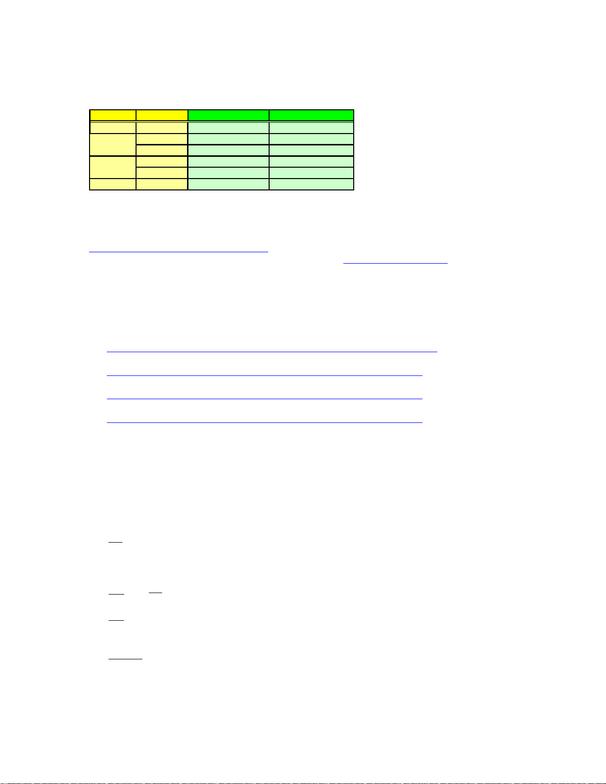
Characteristics PCF8584 PCA9564 Comments PCA9564
Voltage range 4.5 V - 5.5 V 2.3 V - 3.6 V 5 V tolerant
Maximum I
2
to the I
C protocol and send them to I2C devices located on the bus
2
C-bus, convert them to a parallel format and send them to the microcontroller /
microprocessor connected to the controllers
2
2
C -bus specific sequences, protocol, arbitration and timing. The PCF8584 allows parallel-bus systems to
2
C-bus specific transactions with no external timing element required.
2
C freq. 90 kHz 360 kHz Fast-mode I2C compatible
C-bus is carried out on a byte-wise basis using interrupt or polled handshake. It
2
C-bus.
2
C-bus. The PCA9564 can operate as a master or a slave and can be a transmitter
2
C-bus is carried out on a byte-wise basis using interrupt or polled handshake. The
2
C-bus. The PCF8584 provides both master and slave
2
C-bus allowing the 8-bit parallel bus system to
External Internal
Clock source Less expensive and more flexible
TTL (3 to 12
MHz
Parallel interface Compatible with faster processors
Slow Fast
3 MHz 50 MHz
accuracy:
±15
Snoop Mode Yes No
Long Distance Mode Yes No
While the PCF8584 supported most parallel-bus microcontrollers/microprocessors including the Intel 8049/8051,
Motorola 6800/68000 and the Zicor Z80, the PCA9564 has been designed to be very similar to the Philips standard
80C51 microcontroller I
2
C hardware so existing code, for devices such as Philips 8xC552 can be utilized with a few
modifications. There is already code written on the Philips Microcontroller website which would greatly reduce the
software development for the PCA9564. For more information, please check the following URL:
http://www.semiconductors.philips.com/markets/mms/products/microcontrollers/support/software_download/8051/index
.html
Applications
These bus controller devices can be used for a wide variety of applications:
2
I
C-bus Mastering – Some microprocessors have none or an insufficient number of I
be a way to add an I
from the processor to interface to the I
2
the I
C-bus using 2 bits of GPIO, one for the data and one for the clock, if it is the only master on the bus and needs to
2
C port to the microcontroller. The PCF8584 and PCA9564 use 8-bit I/Os and several control signals
2
C-bus in a multiple master capable environment. Any processor can “bit bang”
2
C ports and sometimes there must
3
Page 4

send only simple commands. The PCF8584 or PCA9564 is required when full multiple master compliance with the I
specification is required.
2
I
C-bus Slaving – The PCF8584 and PCA9564 can be used to interface any processor to the I
2
C-bus using 8-bit of
GPIO and some control signals.
2
I
C-bus Sniffing (PCF8584 only) – The PCF8584 provides an I
2
C-bus snoop mode that allows the microprocessor to
monitor communications on the bus without changing the structure.
2
I
C General Call Address (PCF8584 only) – The PCF8584 provides an I
2
C General Call Address mode that allows I2C
General Call Address detection (0x00) when bus controller addressed as a slave.
2
I
C Long Distance Mode (PCF8584 only) -The long-distance mode provides the possibility of longer-distance serial
communication between parallel processors via two I
2
C-bus controllers. In this mode the I2C -bus protocol is transmitted
over 4 unidirectional lines, SDA OUT, SCL IN, SDA IN and SCL IN (pins 2, 3, 4 and 5). These communication lines
should be connected to line drivers/receivers for long-distance applications. Hardware characteristics for long-distance
transmission are then given by the chosen standard. Control of data transmission is the same as in normal I
2
C -bus mode.
Features
PCA9564 Features
• Parallel-bus to I
• Both master and slave functions
• Multi-master capability
• I2C and SMBus compatible
• 2.3 V to 3.6 V operating supply voltage
• 5.5 V tolerant I/Os
• -45 ºC to 85 ºC operating temperature range
• 0 kHz to 360 kHz (400 kHz in slave mode) clock frequency
• Glitch free operation at power-up and power-down, supports hot insertion
• Manufactured in high-volume CMOS process
• ESD protection exceeds 2000 V HBM per JESD22-A114, 200 V MM per JESD22-A115 and 1000 V CDM per
JESD22-C101
• JESDEC Standard JESD78 Latch-up testing exceeds 100mA.
• Offered in 20-pin DIP (N), SO (D), TSSOP (PW) and HVQFN (BS)
PCF8584 Features
• Parallel-bus to I
• Compatible with most parallel-bus microcontrollers/microprocessors including 8049, 8051, 6800, 68000 and Z80
• Both master and slave functions
• Automatic detection and adaptation to bus interface type
• Programmable interrupt vector
• Multi-master capability
2
C-bus monitor mode
• I
2
C-bus All Call Mode
• I
• Long-distance mode (4-wire)
• 4.5 V to 5.5 V operating supply voltage
• -40 °C to +85 °C operating temperature range
• 0 kHz to 90 kHz (100 kHz in slave mode) clock frequency
• Manufactured in high-volume CMOS process
• Offered in 20-pin DIP (P) and SO (T)
2
C -bus protocol converter and interface
2
C -bus protocol converter and interface
2
C
4
Page 5
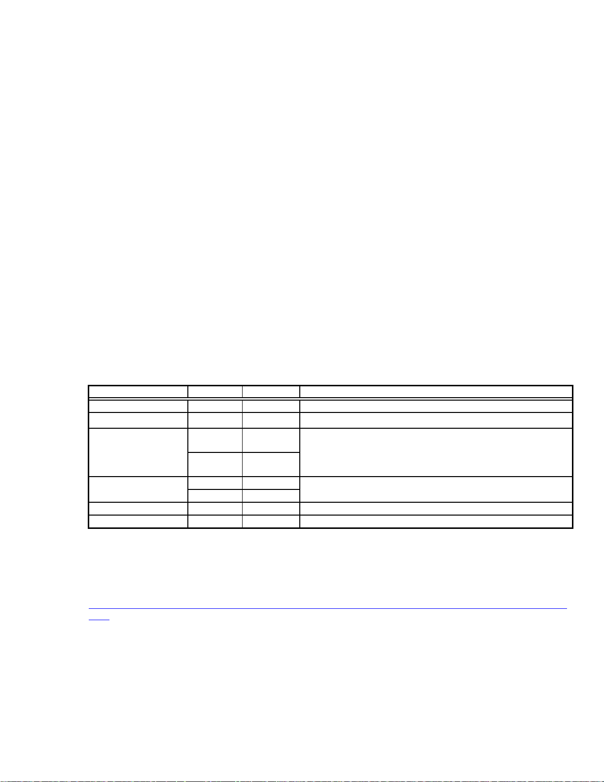
Device Pinout
PCA9564 Pinout
5
Page 6
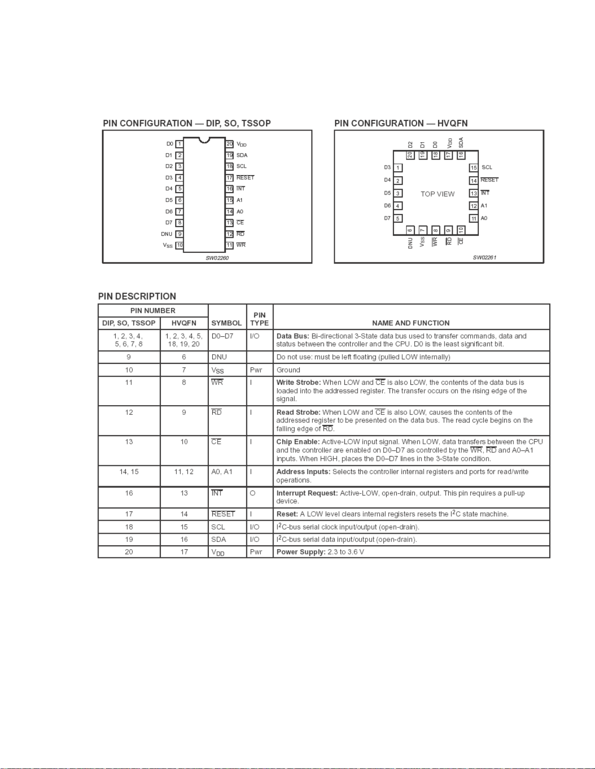
PCF8584 Pinout
6
Page 7
Ordering Information
Package Container
DIP
SO
TSSOP
HVQFN
Tube
Tube PCF8584D PCA9564D
T & R PCF8584D -T PCA9564D -T
Tube Not Available PCA9564P W
T & R Not Available PCA9564P W-T
T & R
PCF8564 PCA9564
PCF8584 PCA9564N
Not Available PCA9564B S-T
Data Sheets and IBIS Models
Data sheet of the PCF8584 and PCA9564 and IBIS model of the PCA9564 can be downloaded from
http://www.standardproducts.philips.com/i2c
PCA9564 HSPICE model is available upon request via email at I2C.Support@philips.com
There are no IBIS and HSPICE models available for the PCF8584.
PCF8584 TECHNICAL INFORMATION
PCF8584 Technical information can be found in the following Philips Application Notes.
• AN425: Interfacing the PCF8584 I
http://www.semiconductors.philips.com/acrobat/applicationnotes/IC22_AN425.pdf
• AN95068: C Routines for the PCx8584
http://www.semiconductors.philips.com/acrobat/applicationnotes/AN95068.pdf
• AN96098: Interfacing 68000 family peripherals to the XA
http://www.semiconductors.philips.com/acrobat/applicationnotes/AN96098.pdf
• AN96040: Using the 8584 with non specified timings and other frequently asked questions
http://www.semiconductors.philips.com/acrobat/applicationnotes/AN96040.pdf
2
C-bus controller to 80C51 family microcontrollers
PCA9564 TECHNICAL INFORMATION
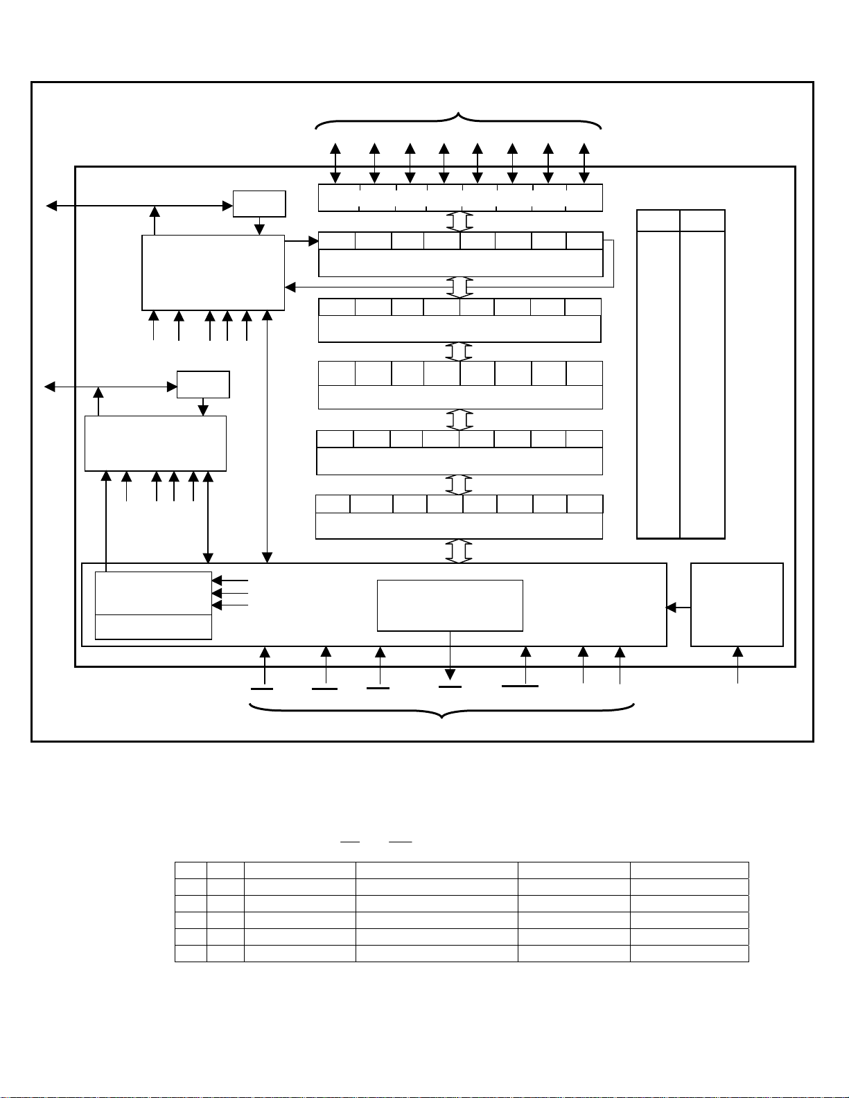
Block diagram
The block diagram of the PCA9564 is shown in Figure 1. Interfacing to the microcontroller, microprocessor or any
device able to communicate with the bus controller (“CPU” will be used from now to designate such a device) and to I
slave or master devices is done through the following pins:
•
: Active-LOW Chip Enable input signal allowing the PCA9564 to communicate with the CPU. This signal may
CE
be held low when it is the only device on the CPU address/data bus.
• D7 to D0: 8-bit bi-directional 3-statable data bus
• A1, A0: Address input pins for internal register-selection
•
and RD: Active-LOW Strobe input signals allowing writing or reading the content of the register addressed
WR
through A1 and A0 pins.
•
: Active-LOW Interrupt output indicating to the master that an event pertinent to the PCA9564 occurred on the
INT
2
C-bus or that an action requested by the CPU has been performed by the PCA9564. Nature of the event or result of
I
the requested action is available by reading the Status register (I2CSTA)
•
RESET
• SDA and SCL: Data and Clock lines of the I
Five internal registers allow the PCA9564 to be configured and data to be sent or received.
An internal 9 MHz oscillator controls I
(Standard-Mode and Fast-Mode I
: Active-LOW Reset input pin clearing the PCA9564 internal registers and resetting the I2C state machine.
2
C-bus timings and generates the I2C clock when the PCA9564 is used as a master
2
C protocol)
2
C-bus
7
2
C
Page 8
K
SDA
SCL
AA
SCL Control
STA STO SI ENSIO
CLOCK
SELECTOR
OSCILLATOR
SDA Control
STA STO SI ENSIO
Filter
Filter
CR0
CR1
CR2
CE
DATA
D7 D6 D5 D4 D3 D2
Bus Buffer
I2CDAT – Data Register – Read / Write
I2CTO – Timeout Register – Write Only
BIT7 BIT5 BIT4 BIT3 BIT2 BIT1 0
BIT6
I2CADR – Own Address – Read / Write
I2CSTA – Status Register – Read Only
AA ENSIO STA STO SI CR2 CR1 CR0
I2CCON – Control Register – Read / Write
INTERRUPT CONTROL
WR
RD
CONTROL SIGNALS
INT
D1
CONTROL BLOC
RESET
Figure 1. PCA9564 Block Diagram
D0
A1
A1 A0
0 1
0 0
1 0
0 0
1 1
A0
POWER
ON
RESET
VDD
Registers definitions
The five internal registers allow the PCA9564 to be configured and data to be sent or received. Definition of the registers
is shown in Table 1. The logic level of pins A1 and A0 determines access to a register. Read or Write operation is
determined by signals applied on pins
A1 A0 Register Name Register Function Read / Write Default Value
0 0 I2CSTA Status Register Read Only 0xF8
0 0 I2CTO Time-out Register Write Only 0xFF
0 1 I2CDAT Data Register Read / Write 0x00
1 0 I2CADR Own Address Register Read / Write 0x00
1 1 I2CCON Control Register Read / Write 0x00
RD and WR .
Table 1. Registers definition
8
Page 9
2
• I2CTO is the time-out register used to determine the maximum time that SCL is low before the I
C state machine is
reset.
Time-Out Period = I2CTO[6:0] x 113.7 µs
The MSB of I2CTO register contains the TE bit.
TE = 0 Time-out function disabled
TE = 1 Time-out function enabled
• I2CADR contains the own address of the CPU connected to the PCA9564 when the device is used in slave mode.
Content of the register is irrelevant when the PCA9564 is functioning as a master.
The seven MSB’s determine the slave address that the PCA9564 will respond to. The LSB should be programmed
with a “0”.
- A “0” in the I2CADR register corresponds to a LOW level in the I
- A “1” in the I2CADR register corresponds to a HIGH level in the I
• I2CDAT contains the byte to be transmitted on the I
In master mode, along with the data byte to be transmitted, it also includes the slave address that the master CPU
wants to send out on the I
2
C-bus: the seven MSB’s are the slave I2C address (SD[7:1] with SD7 as the MSB of the
2
C-bus or a byte that has been received from the I2C-bus.
2
C-bus
2
C-bus
address) while the LSB (SD[0]) is the Read/Write bit.
• I2CCON is the Control Register where the CPU can read from and write to.
A Write to the I2CCON register via the parallel interface automatically clears the SI bit (bit 3), which causes the
Serial Interrupt line to be de-asserted and the next clock pulse on the SCL line to be generated. Since none of the
registers should be written to via the parallel interface once the Serial Interrupt line has been de-asserted, all the
other registers that need to be modified should be written to before the content of the I2CCON register is modified
.
- Bit 7 is the AA bit: Assert Acknowledge Flag
AA = 1 An Acknowledge is sent (Low on SDA) during the Acknowledge clock pulse if:
- The “own slave address” has been received
- A data byte has been received in Master Receiver mode
- A data byte has been received in Addressed Slave Receiver mode
AA = 0 An Acknowledge is not sent (High on SDA) during the Acknowledge clock pulse if:
- The “own slave address” has been received
- A data byte has been received in Master Receiver mode
- A data byte has been received in Addressed Slave Receiver mode
Note:
1. AA bit can be used to temporarily remove the PCA9564 (and the connected CPU) by setting it to “0”.
No acknowledge will then be sent to the device accessing the PCA9564.
- Bit 6 is the ENSIO bit: Enable Serial Input Output (I
2
C-bus)
ENSIO = 1 Serial Input Output enabled – Internal oscillator enabled
ENSIO = 0 Serial Input Output disabled (Hi-Z) – Internal oscillator disabled
Notes:
1. When ENSIO = 0, the PCA9564 is in a “not addressed” slave state and will not respond if its address is
sent by a master on the I
2. When ENSIO = 1, it takes 500 µs for the internal oscillator to stabilize.
3. ENSIO bit should not be used to temporarily remove the PCA9564 form the I
2
C-bus.
2
C-bus since the I2C-bus
status is lost when ENSIO = 0. The AA flag should be used instead as explained above.
- Bit 5 is the STA bit: START command
STA = 1 START command requested – PCA9564 enters Master mode
STA = 0 START command not requested
9
Page 10
Notes:
1. START command is generated when the I
2. If the I
2
C-bus is not free at the request moment, the PCA9564 waits until a STOP command is placed on the
2
C-bus is free.
bus and then generates a START command after the bus free time between a STOP and a START
condition (t
) has elapsed.
BUF
3. If STA is set and the PCA9564 is already in a master mode (and one or more bytes have been sent or
received), the device sends a repeated START command.
- Bit 4 is the STO bit: STOP command
STO = 1 STOP command requested – Bus is free after the t
time has elapsed
BUF
STO = 0 STOP command not requested
Notes:
1. If both STA and STO are set when PCA9564 is in master mode, then a STOP command is generated on the
2
I
C-bus. PCA9564 then generates a START condition after the t
time has elapsed.
BUF
- Bit 3 is the SI bit: Serial Interrupt Flag
SI = 1 Serial Interrupt requested when ENSIO bit is set to 1
The serial interface entered one of 24 of the 25 possible states
(see I2CSTA register definition below)
Serial transfer is suspended
Low period of SCL is stretched
SI = 0 Serial Interrupt not requested
No stretching of SCL
Notes:
1. SI bit must be reset by software (by writing a “0” on that bit)
2. SI bit should never be set to “1” by the user
3. SI bit is not set to 1 when the value in I2CSTA is equal to F8
h
- Bit 2 to Bit 0 are the CR2 to CR0 bits: Clock Rate bits
CR2 CR1 CR0 Serial Clock Frequency (kHz)
0 0 0 330
0 0 1 288
0 1 0 217
0 1 1 146
1 0 0 88
Note 1
1 0 1 59
1 1 0 44
1 1 1 36
Notes:
1. The clock frequency values are approximate and may vary with temperature, supply voltage, process, and
SCL output loading. If normal mode I
2
C parameters must be strictly followed (SCL < 100 kHz), it is
recommended not to use CR[2:0] = 100 (SCL = 88 kHz) since the clock frequency might be slightly higher
than 100 kHz (109 kHz under worst case temperature, voltage, and process conditions) and use CR[2:0] =
101 (SCL = 59 kHz) instead.
2. Clock frequency values in the table are only for master mode. When PCA9564 is used in slave mode, the
device automatically synchronizes with any clock in the I
2
C-bus up to 400 kHz.
• I2CSTA contains the status code. It is a Read Only register and the 3 LSB are always “0”. 25 different codes are
possible and are shown in Table 2. Each code represents a different serial interface state. The first 24 states when
entered sets the SI bit in I2CCON Register to 1 and forces the
INT pin to go low. The 25
th
state (0xF8) does not set
the SI bit to 1 and does not generate an Interrupt because no relevant information is available and no serial interrupt
is then required.
10
Page 11

Status Code
(Hexadecimal)
1 00
2 08 - A START command has been transmitted
3 10 - A repeated START command has been transmitted
4 18
5 20
6 28
7 30
8 38
9 40
10 48
11 50
12 58
13 60
14 68
15 70
16 80
17 88
18 90
19 A0
20 A8
21 B0
22 B8
23 C0
24 C8
25 F8
Note: MT = Master Transmitter, MR = Master Receiver, SR = Slave Receiver, ST = Slave Transmitter
- Bus error due to illegal START or STOP command
- Address+W has been transmitted
- ACK has been received
- Address+W has been transmitted
- NACK has been received
- Data byte in I2CDAT has been transmitted
- ACK has been received
- Data byte in I2CDAT has been transmitted
- NACK has been received
- Arbitration lost in Address+W or Data byte
- Arbitration lost in Address+R or Data byte
- Arbitration lost in NACK bit
- Address+R has been transmitted
- ACK has been received
- Address+R has been transmitted
- NACK has been received
- Data byte has been received
- ACK has been returned
- Data has been received
- NACK has been returned
- Own Address+W has been received
- ACK has been returned
- Arbitration lost in Address+RorW as master
- Own Address+W has been received
- ACK has been returned
- Bus error, SDA stuck low
- Previously addressed with Own Address
- Data byte has been received
- ACK has been returned
- Previously addressed with Own Address
- Data byte has been received
- NACK has been returned
- Bus error, SCL stuck low
- A STOP or Repeated START command has been
detected while still addressed in SR mode
- Own Address+R has been received
- ACK has been returned
- Arbitration lost in Address+RorW as master
- Own Address+R has been received
- ACK has been returned
- Data byte in I2CDAT has been transmitted
- ACK has been received
- Data byte in I2CDAT has been transmitted
- NACK has been received
- Last data byte in I2CDAT has been transmitted (AA=0)
- ACK has been received
- Reset or STOP command
Table 2. Status Codes – I2CDAT Register
Status
MT MR SR ST
• • • •
•
•
•
•
•
• •
• •
• • • •
Mode
•
•
•
•
•
•
•
•
•
•
•
•
•
•
•
•
11
Page 12

Read and Write Strobes
r
t
U
Read and Write strobes are used to select the type of operation that needs to be performed on the selected register.
D[7:0]
Floating
Data from CPU
Floating
A[1:0]
Floating Address
Floating
Address
WR
RD
CE
ADDRESS LATCHED ADDRESS LATCHED
DATA WRITE
Address is latched when WRis going
low.
Data are written to the addressed registe
on the rising edge. Data must be stable a
that time.
Figure 2. Read and Write Strobes
Data available
DATA
READ
Address is latched when RD is going
low.
Data from the PCA9564 becomes
available after 17 ns max. The CP
can then read data from the PCA9564.
When
RD is going high, data bus
floating after 17 ns max.
Floating
Floating
Polling SI bit versus using INT pin as Interrupt
Interfacing and control of the I2C-bus operation can be done by either:
• Polling the SI bit by reading I2CCON Register.
- When SI is at 0, no new state has been generated or detected by the PCA9564 and SCL clock line is not held
low by the PCA9564
- When SI is at logic 1, a new state has been generated or detected by the PCA9564. SCL clock line is held low
by the PCA9564 (Clock stretching) and action by the CPU is required. To leave the “clock stretched” state, SI
bit must be reset by the CPU (write a “0”).
• Using the
- When
held low by the PCA9564
- When
by the PCA9564 (Clock stretching) and action by the CPU is required. To clear the Interrupt, SI bit must be
reset by the CPU (write a “0”).
pin as Interrupt function
INT
is High, no new state has been generated or detected by the PCA9564 and SCL clock line is not
INT
goes low, a new state has been generated or detected by the PCA9564. SCL clock line is held low
INT
12
Page 13

)
d
p
w
•
N
START
SI = 0, INT = 1
Power Up
Power Up default state
I2CCON = 0x00
CPU command
Initialization
See Figure 5. PCA9564 Initialization
PCA9564 initialized and ready to:
- Execute commands from the CPU
(START, STOP, Send/Receive Data)
- Recognize I
2
C traffic/command targeting it
Method 1:
CPU polls the SI bit (loop on I2CCON Register
Read until SI = 1
When SI = 1:
• The request from the CPU has been performed
by the PCA9564, or
• PCA9564 detected an a command targeting it
• The I2CSTA register contains new Status
•
INT
• SCL line is held low (clock stretching)
pin goes low
Method 2:
CPU waits until /INT pin goes low
When INT goes low:
• The request from the CPU has been performed by
the PCA9564, or
• PCA9564 detected an a command targeting it
• I2CSTA register updated with the new Status
• SI bit is set to 1
• SCL line is held low (clock stretching)
Important note:
SI bit is not set to 1 an
INT
in does not go Lo
when I2CSTA register is
loaded with F8
.
H
Read I2CSTA
Read I2CSTA: SI = 1 and pin INT Low
Write I2CCON Register
SI = 0
SI = 0
pin goes High
•
INT
• SCL not stretched
SI = 0 allows to clear the Interrupt condition
ote: a Write to I2CCON Register automatically clears SI bit
Figure 3. SI bit and
INT pin
Reset
An active low Reset allows to
- Clear all internal registers to their default values
- Reset the I
2
C-bus state machine
Reset pulse must be at least 100 ns long (Low state) to reset the device
Interfacing the PCA9564 with CPU and slave devices – Hardware
• Power supply: The PCA9564 is a 3.3V device and all the I/O’s are 5 V tolerant. This allows the device to interface
with 5 V CPU and 5 V I
• Interfacing with the I
SCL and SDA pins are open drain and must be connected to pull-up resistors. Pull-up resistors must be chosen to
satisfy:
- 3 mA drive capability with V
- Rise time max at 1 µs for Standard-Mode I
max capacitive load
2
C devices.
2
C devices:
at 0.4 V
OL
2
C protocol and 0.3 µs for Standard-Mode I2C protocol, for a 400 pF
13
Page 14

• Interfacing with the CPU:
- Data bus (D7 to D0), Address pins (A1 and A0), Chip Enable, Read and Write control signals (
CE , RD and
WR ), Reset pin ( RESET ) are a function of the I/O architecture of the CPU used.
-
INT is open drain and requires a pull-up resistor if the CPU pin connected to it does not have any
Interfacing the PCA9564 with CPU and slave devices – Software
An evaluation board with some embedded code is available at
http://www.standardproducts.philips.com/support/boards/pca9564. Block diagram is shown in Figure 4.
The evaluation board includes:
- A Philips P89LV51RA2 microcontroller
- A Philips PCA9564 interfacing with the P89LV51RA2 microcontroller
2
The I
C-bus has the following devices:
- A Philips P89LPC932 microcontroller able to be either an I
- A Philips PCF85116 I
- A Philips PCA9531 I
- A Philips PCA9554 I
2
Two I
C connectors allow connection to daughter cards with other I2C master and/or slave devices
2
C 16 kbits EEPROM
2
C 8-bit LED dimmer
2
C 8-bit GPIO collecting program selection information through 8 pushbuttons
Code can be downloaded to the 2 microcontrollers through a RS232 connector (ISP programming).
Sample code will show:
- How to create some dimming/blinking patterns using the P89LV51RA2 + PCA9564 + PCA9531 + PCF85116
- The multi-master capability of the PCA9564 using the P89LV51RA2 and the P89LPC932 as 2 masters trying to take
control of the bus at the same time.
For more information on the evaluation board and the sample code, consult Application Note AN10149 and the fllowing
link:
http://www.standardproducts.philips.com/support/boards/pca9564
2
C Connector (To Daughter Cards)
I
P89LV51Rx2
DATA
CONTROL
RS232
Connector
SP3223
Figure 4. PCA9564 evaluation block diagram
2
C slave or an I2C master
2
I
C
PCF85116
PCA9564
PCA9531
P89LPC932
INT
PCA9554
Pushbuttons for program selection
LEDs
LEDs
14
Page 15

Master and Slave modes handling
Master or Slave mode is automatically handled by the PCA9564. When the bus is idle (SDA = SCL = 1, before a
START command or after a STOP command), the PCA9564 is in:
- Active slave-receiving mode when ENSIO = 1 and AA = 1
- Passive slave-receiving mode when ENSIO = 1 and AA = 0
- Disabled mode in the bus when ENSIO = 0
From an idle situation, there are 3 possible scenarios:
1. The device (for example, µcontroller) connected to the parallel port of the PCA9564 requests a START command
(STA = 1, ENSIO = 1). The PCA9564 is then automatically configured in master mode until the device
(µcontroller) requests a STOP command and the PCA9564 sends it (then causing the I
condition) or if PCA9564 loses arbitration to another master (see scenario 3).
2. A master connected to the I
2
C-bus sends a START command, followed by the slave address of the PCA9564
(assuming the PCA9564 I2CADR register has been previously programmed with its slave address).
- If ENSIO = 1 and AA = 1, the PCA9564 is then automatically configured in active slave mode (receiver or
transmitter depending of the LSB of the I
master located in the I
2
C-bus (then causing the I2C-bus to be in an idle condition). Active slave mode means
that the PCA9564 acknowledges its I
2
C address byte) and will stay so until a STOP command is sent by the
2
C address and will either send or receive data (depending of the R/W bit
value) at the speed determined by the SCL signal.
- If ENSIO = 1 and AA = 0, the PCA9564 is then automatically configured in passive slave mode and will stay
so until a STOP command is sent by the master connected to the I
idle condition). Passive slave mode means that the PCA9564’s SIO (Serial I/O) can be temporarily released
(virtually disconnected) from the I
running and the SIO can be connected back to the bus at any time by setting the AA bit. When AA = 0, the
PCA9564 does not acknowledge its I
2
C-bus without completely disabling it, i.e. the internal oscillator is still
2
C address and will stay “quiet” until the master has sent a STOP
2
C-bus (then causing the I2C-bus to be in an
command.
- If ENSIO = 0, the PCA9564 is in disabled mode. The internal clock is disabled, the PCA9564 is virtually
disconnected from the I
3. In a multi-master configuration, both sides of the PCA9564 (parallel and I
2
C-bus and its state machine is not synchronized with what is happening on the I2C-bus.
2
C) try to take control of the bus, thus
causing the PCA9564 to start an arbitration procedure. The arbitration will end with one of the following:
- The PCA9564 enters master mode (it won the arbitration, same as scenario 1 above)
- The PCA9564 enters slave mode (it lost the arbitration and the other master addresses the PCA9564, same as
scenario 2 above)
- The PCA9564 enters master-in-waiting mode, where the PCA9564 is waiting for the other master (that won
arbitration) to complete its transaction so that it can once again try to gain control of the I
2
C-bus to be in an idle
2
C-bus.
15
Page 16

FLOWCHARTS
r
Initialization Sequence
Delay: wait a time equal to the
longest I
(Multimaster systems only)
Reset 100 ns
TIMEOUT REGISTER
I2CTO =0xFF
OWN ADDRESS
I2CADR = 0x64
ENABLE SERIAL IO
I2CCON = 0x44
Wait 500 µs
READ BACK REGISTERS
2
C message
I2CCON = 0xC4
START
END
A0 = 0
A1 = 0
A0 = 0
A1 = 1
A0 = 1
A1 = 1
A0 = 1
A1 = 1
Set own address for use as a slave
Clock Frequency set at 88 kHz
Wait for Oscillator Startup
Optional verification – allows verification of the
previous programming
At power-up, if a PCA9564 node is powered-up slightly afte
another node has already begun an I2C-bus transmission, the bus
busy condition will not have been detected. Thus, introducing this
delay will insure that this condition will not occur.
Slave receiver mode
AA = 1, ENSIO = 1, SI = 0
Figure 5. PCA9564 Initialization
16
Page 17

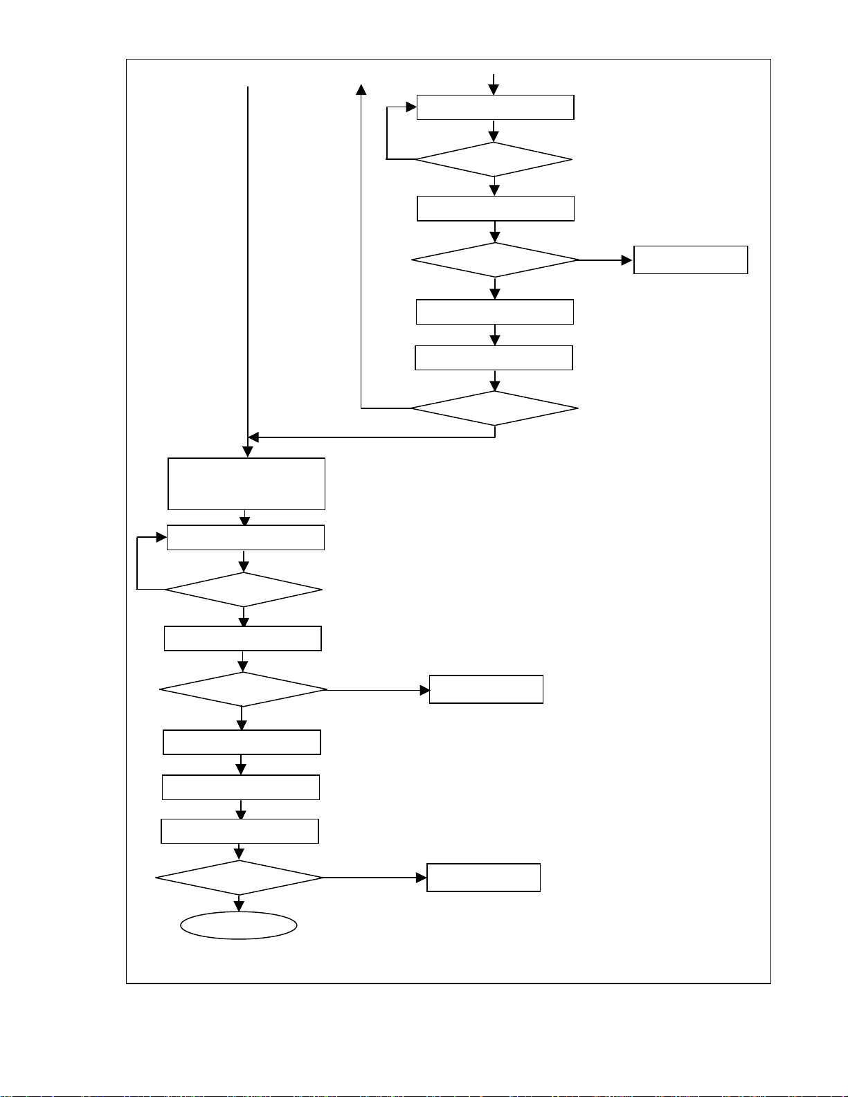
Master Transmitter Mode
N
N
N
N
In this flow chart, I2C clock frequency is programmed to run at 88 kHz (I2CCON Register, bits CR [2:0] = 100)
`
O
Load Slave Address + R/W bit = 0
Reset SI and STA bits in I2CCON
O
N = number of bytes to be transferred
M = number of bytes transferred = 0
Load data into I2CDAT
Reset SI bit in I2CCON
Write I2CCON = 0xC4
Continued on next page – Figure 6b
START
Write I2CCON = 0xE4
Read I2CCON
SI = 1?
YES
Read I2CSTA
I2CSTA = 0x08?
YES
into I2CDAT
Write I2CCON = 0xC4
Read I2CCON
SI = 1?
YES
Read I2CSTA
I2CSTA = 0x18?
YES
Figure 6a. Master Transmitter Mode
A0 = 1
A1 = 1
A0 = 1
A1 = 1
A0 = 0
A1 = 0
O
A0 = 1
A1 = 0
A0 = 1
A1 = 1
A0 = 1
A1 = 1
A0 = 0
A1 = 0
A0 = 1
A1 = 0
A0 = 1
A1 = 1
O
Generate START command
AA = 1, ENSIO = 1, STA = 1
Poll from transmission finished
FAULT HANDLER
Send Slave address + Write Command
AA = 1, ENSIO = 1
Poll from transmission finished
FAULT HANDLER
Data to be sent is loaded I2CDAT register
Send Data
AA = 1, ENSIO = 1
17
Page 18

N
N
N
N
Continued from previous page – Master Transmitter mode
Read I2CCON
A0 = 1
A1 = 1
O
SI = 1?
YES
Read I2CSTA
A0 = 0
A1 = 0
Poll from transmission finished
I2CSTA = 0x28?
YES
M = M + 1
O
FAULT HANDLER
O
N = M?
YES
Write I2CCON = 0xD4
A0 = 1
A1 = 1
Generate STOP command
AA = 1, ENSIO = 1, STO = 1
Read I2CCON
A0 = 1
A1 = 1
STO = 0?
YES
END
O
FAULT HANDLER
Slave receiver mode
AA =1, ENSIO = 1, SI = 0, Clock Frequency = 88 kHz
STO bit resets itself once the
STOP command is sent
Figure 6b. Master transmitter Mode
18
Page 19

N
N
N
N
N
Master Receiver Mode
In this flow chart, I2C clock frequency is programmed to run at 88 kHz (I2CCON Register, bits CR [2:0] = 100)
O
Load Slave Address + R/W bit = 1
Reset SI and STA bits in I2CCON
O
N = number of bytes to be transferred
M = number of bytes transferred = 0
START
Write I2CCON = 0xE4
Read I2CCON
SI = 1?
YES
Read I2CSTA
I2CSTA = 0x08?
YES
into I2CDAT
Write I2CDAT
Write I2CCON = 0xC4
Read I2CCON
SI = 1?
YES
Read I2CSTA
I2CSTA= 0x40?
YES
N = 1?
YES
A0 = 1
A1 = 1
A0 = 1
A1 = 1
A0 = 0
A1 = 0
A0 = 1
A1 = 0
A0 = 1
Continued on next page – Figure 7b
A1 = 1
A0 = 1
A1 = 1
A0 = 0
A1 = 0
O
Generate START command
AA = 1, ENSIO = 1, STA = 1
Poll from transmission finished
O
Send Slave address + Read Command
AA = 1, ENSIO = 1
Poll from transmission finished
O
Figure 7a. Master Receiver Mode
FAULT HANDLER
FAULT HANDLER
Reset SI bit and set AA bit in
I2CCON
Write I2CCON = 0xC4
A0 = 1
A1 = 1
Read Data
AA = 1, ENSIO = 1
19
Page 20
N
Continued from previous page – Master Receiver mode
N
N
N
N
N
Read I2CCON
O
SI = 1?
YES
Read I2CSTA
A0 = 1
A1 = 1
A0 = 0
A1 = 0
Poll from transmission finished
A0 = 1
A1 = 0
O
FAULT HANDLER
Data read from the I2C bus can be
read from I2CDAT register
I2CSTA = 0x50?
YES
Read data from I2CDAT
M = M + 1
Reset SI and AA bits in I2CCON
Write I2CCON = 0x44
A0 = 1
A1 = 1
Read I2CCON
A0 = 1
A1 = 1
O
The last byte of the transmission is not
acknowledged
AA = 0, ENSIO = 1
Read Data
M = N - 1?
YES
O
SI = 1?
YES
Read I2CSTA
A0 = 0
A1 = 0
Poll from transmission finished
I2CSTA = 0x58?
YES
Read Data from I2CDAT
A0 = 1
A1 = 0
O
FAULT HANDLER
Data read from the I2C bus can be
read from I2CDAT register
Write I2CCON = 0xD4
A0 = 1
A1 = 1
Generate STOP command
AA = 1, ENSIO = 1, STO = 1
Read I2CCON
STO = 0?
YES
END
A0 = 1
A1 = 1
O
FAULT HANDLER
Slave receiver mode
AA =1, ENSIO = 1, SI = 0, Clock Frequency = 88 kHz
STO bit resets itself once the
STOP command is sent
Figure 7b. Master Receiver Mode
20
Page 21

Slave Transmitter / Receiver mode
N
N
N
N
N
N
N
N
N
A0 = 1
A1 = 1
A0 = 1
A1 = 1
A0 = 0
A1 = 0
A0 = 1
A1 = 0
O
Read Data from I2CDAT
START
Read I2CCON
SI = 1?
YES
Read I2CSTA
I2CSTA = 0x60?
YES
Reset SI bit in I2CCON
Write I2CCON = 0xC4
Read I2CCON
SI = 1?
YES
Read I2CSTA
I2CSTA
= 0x80?
YES
Data read from the bus
can be read from
I2CDAT Register
A0 = 1
A1 = 1
A0 = 1
A1 = 1
A0 = 0
A1 = 0
O
Slave Receiver Mode
O
Read Data or Command from the bus
AA = 1, ENSIO = 1
O
FAULT HANDLER
I2CSTA
= 0xA0
Write I2CCON = 0xC4
END
Figure 8. Slave Receiver / Slave Transmitter Modes
Assumption: PCA9564 is in Slave Receiver Mode
I2CCON = 0xC4 (AA = 1, ENSIO = 1, Clock Frequency = 88 kHz)
Own slave address already loaded in I2CADR (see Figure 5 – PCA9564 Initialization)
Poll from transmission finished
O
?
YES
Slave Receiver Mode
AA =1, ENSIO = 1, SI = 0, Clock Frequency = 88 kHz
Slave Transmitter Mode
Send Data on the bus
AA = 1, ENSIO = 1
FAULT HANDLER
O
I2CSTA
= 0xC0?
YES
I2CSTA = 0xA8?
YES
Load I2CDAT with Data
Reset SI bit and set AA bit in
I2CCON = 0xC4
Read I2CCON
O
Read I2CSTA
O
I2CCON
SI = 1?
I2CSTA
= 0xB8?
FAULT HANDLER
YES
YES
O
A0 = 1
A1 = 0
A0 = 1
A1 = 1
A0 = 1
A1 = 1
A0 = 0
A1 = 0
21
Page 22

Time-out – SCL Stuck Low Error
Command?
)
N
p
N
N
p
N
N
N
N
N
N
N
N
PCA9564 integrates a “SCL Low” sensing feature that generates a “SCL Stuck Low” error (90H) when activated (TE bit
in I2CTO Register = 1) and the clock line stays low longer than the TimeOut Value programmed on I2CTO register.
O
YES
Count TimeOutCount
- Reset TimeOutCount
- Send START
Command (Send
LOW SDA
- I2CSTA = 0x08
-
INT = Low
- SI = 1
Read I2CSTA (08H)
START
Command
START
YES
Bus idle?
YES
Bus idle and
STOP
detected?
O
TimeOutCount >
TimeOutValue?
YES
START, STOP, Send / Receive Data
ENSIO = 1, SI = 0
STA = 1 if START Command
STO = 1 if STOP Command
O
O
- Send LOW SCL
- Send Data on SDA if Write
- Send Low on SDA if STOP
Command
- Count SCLCount
- Count TimeOutCount
O
O
SCLCount
> Half SCL
Release SCL
SCL = HIGH?
Keep counting TimeOutCount
TimeOutCount >
TimeOutValue?
Timeout on SCL
detected
SCL is stuck low
- Reset TimeOutCount
I2CSTA = 0x90
-
- INT = Low
- Set SI bit at 1
- Release SDA and SCL
Read I2CSTA (90H)
Reset PCA9564
RESET = Low
- Reset SCLCount
Figure 9. Timeout Flowchart
eriod?
YES
YES
otes:
1. Time-out feature enabled (TE=1)
2. Time-out register loaded with TimeOutValue (7 bits)
3. Valid for Master Mode
CPU Command
YES
O
- Count SCLCount
- Receive Data if Read Mode
- Receive ACK or NACK if
- Send ACK or NACK if Read
O
STOP
Command?
O
Reset TimeOutCount
Write Mode and ACK Phase
Mode and ACK Phase
SCLCount
eriod?
> SCL
YES
Command fully
YES
Send Low SCL
-
Release SDA
-
Reset SCLCount
-
- Update I2CSTA
INT = Low
-
- SI = 1
Read I2CSTA
YES
- Release SDA
- Reset TimeOutCount
- Reset SCLCount
END
O
22
Page 23

Bus Recovery – SDA Stuck Low Error
K
K
p
N
S
ow
d
d
N
N
eceiving data (byte+ACK)?
N
N
A built-in bus recovery feature allows the PCA9564 to initiate automatically a recovery attempt from a “SDA Stuck
Low” situation. If the attempt is unsuccessful, a “SDA Stuck Low” error (70
START Command
ENSIO = 1, SI = 0, STA = 1
SDA Stuck Low Detected
- Send 9 SCL Clock Pulses
- Keep PCA9564 SDA
released
The 9 clock pulses will make the hanging
device’s state machine move to the next state
after each clock pulse while the PCA9564 SDA
released (not pulled down) will cause a NAC
when the state machine will move to the AC
hase. The NACK will force the device to go
to idle mode
Generate a STOP command
If the bus recovery has been successful,
the bus is now idle (SDA = SCL = 1) an
a STOP command can be generated
SDA Stuck
O
Generate START Command
- I2CSTA = 0x70
- INT = Low
- Set SI bit at 1
- Release SDA and SCL
YES
Bus recovery has not been successful an
a “Bus Stuck Low” error needs to be
generated
Read I2CSTA (70H)
Reset PCA9564
RE
ET = L
Figure 10. Bus recovery Flowchart
) is generated.
H
ote:
1. Valid for Master Mode
CPU Command
Bus error
A “Bus Error” error (00H) is generated by the PCA9564 every time an illegal command is generated.
Command
Command = STOP
and sent right after
START?
YES
- I2CSTA = 0x00
- INT = Low
- Set SI bit at 1
- Release SDA and SCL
Figure 11. Bus error Flowchart
O
Read I2CSTA (00H)
Reset PCA9564
RESET = Low
23
Command = STOP or
START when sending or
r
YES
ote:
1. Valid for Master and Slave Modes
CPU Command
O
Valid
Command
Page 24

APPLICATIONS
Typical Application using the 80C51 microcontroller
Figure 12 shows the PCA9564 in a typical application. Interfacing is simple to realize and requires minimal external
devices.
Figure 12. PCA9564 using the 80C51
Interfacing the PCA9564 to send/receive I2C commands over long cables
Figure 13 shows an application of PCA9564 used in conjunction with Philips P82B96 Bus buffers to send I2C commands
through long cables to slave ICs.
Figure 13. PCA9564 with P82B96 for long distance application
In such I
The existing I
enclosure. When we introduce delays we need to design to ensure the necessary bus timings will still be met. See
Figure 14 for one example of the necessary timing.
2
C systems, we introduce bus propagation delays into the SCL and SDA signals.
2
C specifications do not expect bus delays because they were written for small systems inside one
24
Page 25

Figure 14. Illustrating the allowed delay time that needs to be considered
The following example shows how to calculate the longest allowed cable based on PCA9564 running at the maximum
speed of 400 kHz (nominal 330 kHz with the limits of tolerances applied). When even longer cables are needed the bus
speed must be reduced.
Two bus signal propagation delays are introduced:
1. Propagation delays caused by buffering with P82B96
2. Cable propagation delays.
Flat 4-core telephone cable makes a convenient cable for I
2
C signals. The logic signals should be separated by a ground
or supply wire so the signals across the cable might be chosen in the order Ground, SCL, 5V, SDA. The characteristic
impedance of the transmission lines will probably be in the 75-150 Ω range, and will not be equal due to their
asymmetry. The allowed pull-up resistors will be greater than the correct termination impedance, especially if the pullups are split, for symmetry, by putting half the pull-up at each end of the link. For 5V operation, the lowest resistance
allowed at each end of the cable is (5 V – 0.4 V) / 15 mA = 307 Ω and it is best to use the nearest convenient value,
316 Ω or 330 Ω. Plastic cable propagation delays are about 5 ns/m. We need to consider the “round trip” delays, meaning
the sum of SCL signal delays from master to slave then the SDA reply signal delays back to the master. So for each
meter of cable, the “round trip” signal delay will be 10 ns.
The delays associated with the P82B96 buffering include its internal logic propagation delays (about 300 ns from master
to slave, and 300 ns from slave back to master because the signals in each direction will travel through two devices) plus
“effective” propagation delays caused by bus rise and fall times if there is significant local bus capacitive loading at the
ends of the cables. Each device will cause about 200 ns delay for signals in one direction and less than 80 ns in the other
direction, the total is less than 300 ns.
Because the delays will be almost identical on the SCL and SDA lines, and PCA9564 supports “clock stretching”, about
half of the propagation delay introduced by P82B96 on the SCL wire does not need to be considered. When it delays the
rise of the SCL line at the master (PCA9564), the master will simply adjust its timings to take account of that delay.
The important delays are:
1. The effective delay of the falling edge of the SCL signal from the PCA9564 to the slave and
2. The effective delay of a rising edge of SDA information from a slave back to the PCA9564.
These are usually the longest delay times that effectively reduce the timing margins of I
2
C signals.
25
Page 26

(A falling edge generated by a slave usually has a faster fall time than the corresponding (passive) bus rise time, so the
rise time case becomes the design limit. A delay of the rising edge of the SCL is an allowed “clock stretching”.)
Consider:
1. The SCL falling edge propagation to the slave. PCA9564 drives Sx low, the low at Sx propagates to Tx with less
than 80 ns delay. Tx has powerful sinking capability and will drive the cable past the logic low threshold in about
20 ns. The low propagates to the distant P82B96 after a cable delay of 5ns/meter. The received low at Rx propagates
to Sx on the slave I
2
C-bus with about 200 ns delay. Total delay = 80 ns + 20 ns + 200 ns + 5 ns/m = 300 ns +
5 ns/m.
2. When the slave receives the SCL low it responds with an ACK pulse or data on its SDA line. Most Philips slave
parts will respond in less than 600 ns (See AN255 Appendix 7). I/O expanders and LED drivers e.g. PCA9554 or
PCA9550 respond in less than 375 ns. We need to consider the worst case where a slave outputs a “1” and the SDA
line needs to rise from a low.
The slave SDA line at Sx rises to 0.65 V and that high level at Sx propagates through P82B96 in 80 ns to release its
Tx pin. The cable at Tx will rise with a time constant that depends on any local capacitance and the pull-up resistor
in parallel with the cable’s characteristic impedance. The maximum allowed rise time is 300 ns (measured between
30% and 70% of V
) but to allow for buffer/cable delays it is necessary to design for much shorter times. It is
CC
difficult (without simulations) to accurately predict the signals on improperly terminated transmission lines but in
practice it is easy to achieve the more practical cable rise time (i.e. its 0-50% rise time) in less than 50 ns by using
minimum pull-up resistors (30 mA total sink current).
The cable delays will not exceed 5 ns/m, but don’t be surprised if, due to reflection effects, the Rx pin crosses Vcc/2
at the far end before it reaches that level at the end that generates the signal!
The signal from the cable connected at Rx propagates to Sx (connected to PCA9564) with a delay less than 200 ns.
So the total propagation delay of the SDA signal = 80 ns + 50 ns + 5 ns/m. + 200 ns = 330 ns + 5 ns/m.
The slave response delay may be measured, or taken as less than 600 ns for most Philips parts.
The delay in the rise of Sx on the SCL connection at the PCA9564 is calculated as follows:
- PCA9564 releases Sx
- Sx rises to the high threshold at Sx = 0.65 V, this high at Sx propagates to Tx after a delay about 80 ns.
- Tx releases the cable and the cable input voltage rises to half rail in typically 30 ns.
- That high at Rx propagates back to release the SCL line at Sx after a delay about 200 ns.
So the total “clock stretch” = 80 ns + 30 ns + 200 ns = 310 ns.
The total (effective) delay introduced into the data signal returning from a slave is calculated as:
Propagation delay of SCL falling edge from PCA9564 to the slave – compensating local clock stretch effect at the
PCA9564 + slave response time + delay of an SDA rising edge of data sent from a slave to PCA9564.
Effective delay (ns) = (300 ns + 5 ns/m) – 310 ns + Slave response time + (330 ns + 5 ns/m) = slave response time plus
(320 ns + 10 ns/m)
The available response time for 400 kHz operation = minimum clock low period – data set-up time = 1300 ns – 100 ns =
1200 ns.
The safety margin available to be used for introduced delays (assuming a 600 ns slave response time) = 1200 ns – 600 ns
– 320 ns – 10 ns/m = 280 ns – 10 ns/m.
This would allow a maximum cable length of 28 m, for full 400 kHz operation.
Notice that no allowance is made until now for the rise/fall times of the buses connected at Sx at the master and slave.
When these are 3.3 V buses, that permit pull-up resistors of around 1 kΩ, practical rise and fall times with say 50 pF
loading can be kept to less than 80 ns total.
That means practical cable lengths up to at least 20 m, having 200 ns propagation delay, are possible when operated with
5 V logic and slaves with delays up to 600 ns. For greater noise immunity, it is also allowable to use 12 V logic levels on
the cable but with such fast switching and unshielded the possible radiated interference also should be considered.
In practice these calculations provide quite large safety margins. For example PCA9564 does not actually use the SDA
signal until about 180 ns after the SCL rising edge while our calculations, based on the general I
2
C requirements, have
allowed 100 ns set-up time. That provides some 280 ns of additional safety margin.
And when PCA9564 is operating at its normal master speed of 330 kHz there will be an additional clock low time of
276 ns, providing another very large factor of safety. At the nominal 330 kHz a typical cable could be over 70 meters
long.
26
Page 27

PCA9564 EVALUATION BOARD
An evaluation board for the PCA9564 device has been designed and is available free of charge (while supplies last)
through your local Philips Sales office or by sending an email to: I2C.Support@philips.com.
More information can be found at the PCA9564 Evaluation Board main web page:
http://www.standardproducts.philips.com/support/boards/pca9564
FREQUENTLY ASKED QUESTIONS
1. Question: We are planning on using the PCA9564. Does this device support Hot Insertion (i.e., the SCL and SDA
pins receive a signal before power is up)?
Answer: The PCA9564 would be OK, in the sense that it should not do anything to the bus until the power-up
sequence is finished and the part is programmed to do so. There could be some drooping of the bus lines as the part
is added to the line and the SCL/SDA pin capacitance is charged.
2. Question: What happens to the PCA9564 and the PCF8584 if they are inserted to an active I
that they will not be well initialized and will not recognize that the bus is busy.
Answer: Both the PCF8584 and PCA9564 will be in an incorrect initialization state if they are inserted into a
system in the middle of an I
2
C transmission. Both devices need to see the Start condition to recognize that the bus is
busy. For that, it is a good design practice to introduce a delay at least equal to the longest I
up before starting any operation. Introducing this delay will insure that the bus controller will detect correctly the
“bus busy” condition.
3. Question: We have begun to work with the PCA9564 Parallel ↔ I2C converter in our application and we noticed
that there is no specific mention of the handling of the General Call Address in the specification. Is this device able
to process messages from the general call address as well as its specific node address (set by software)?
Answer: The PCA9564 has not been designed to respond to the General Call Address. When such a command is
generated in the bus, the PCA9564 will ignore it, will not acknowledge and no further action will be taken during
the sequence.
4. Question: The PCA9564 does not seem to include a bus monitor mode. Is it only the PCF8584 that has this
capability?
Answer: Yes, the PCF8584 can monitor the bus, but the PCA9564 cannot. This feature was not included in the
PCA9564 to make the part less complex.
5. Question: Prior to changing the design over to the PCA9564, we had planned to use the PCF8584. It was my
understanding the PCF8584 was not recommended for new designs. Is that the case?
Answer: The PCF8584 is recommended for new designs. It is usually always better to move to the newer devices
for new design since they would give the greatest life span, but since the PCA9564 doesn't have the snoop mode,
long distance mode, all call and can't work at 5 V AND the PCF8584 is currently being used in many different
segments in cumulative large volumes, the PCF8584 is not going to be obsolete for 5-10 years if then, so please feel
free to use it for your new design without worrying about EOL issues.
6. Question: How do masters know who they are (how is their address assigned)?
Answer: Masters do not have addresses unless they can also be slaves. The system architect reviews all I
devices that will operate within the system and which I
then writes firmware in C or Assembly language that includes the specific 7-digit I
2
C address each slave device will be assigned. The designer
2
C address for that master/slave
device. The firmware is loaded into the microcontroller in three possible ways:
1) Mask programmable by manufacturer (e.g., Philips Semiconductors),
2) OTP on test bench by manufacturer or done locally
3) Sent to device and stored in flash (EEPROM like memory) by manufacturer or done locally.
When the microcontroller powers up, the firmware will assign the slave address to the device (127 different
addresses are possible). If the microcontroller does not have an I
PCF8584 or PCA9564 to interface with the I
2
C-bus. The bus controllers are programmed by the microcontroller at
2
C port, it can use a bus controller device like the
start up through the 8 parallel I/O pins with the slave address in the firmware. The bus controller's slave address is
stored in the “Own Address” register in the PCF8584 and the “I2CADR” register in the PCA9564.
2
C-bus? It seems to me
2
C transmission at power
2
C slave
27
Page 28

7. Question: What happens when the master connected to the PCA9564 initiates an I
a START condition and that the SDA line is LOW because an I
2
C device downstream is holding the line (stuck
situation)? Can the PCA9564 manage this situation or does it only report a “SDA Stuck Low” status?
Answer: The PCA9564 is capable of sending out 9 clock pulses and a STOP condition on the I
2
C communication by requesting
2
C-bus (when it has
been requested to send a START condition and the SDA line is LOW). It will then look at the SDA line again and
check if the line has gone HIGH after this particular sequence. If not, it will report an error condition. If the SDA
line has gone HIGH, it will go ahead and send a START condition on the I
2
C-bus. This was designed in specifically
for the situation in which a slave is holding the SDA line low because it is stuck in a READ operation and is sending
out a LOW (zero) to the master but does not receive any further clock cycles followed by a NACK to reset itself.
8. Question: I want to know if Philips Semiconductors has an I
Answer: I don't know of any bus controller that handles 3.4 MHz. The bus controller is used to interface a
Microcontroller to the I
2
C-bus in a multiple master application since it supports all master modes. In simple systems
with only one master it would be possible to bit bang the I
2
C-bus controller for high-speed mode – 3.4 MHz?
2
C-bus using two I/O ports on the micro. This allows the
higher bus speeds assuming the slave is rated for the High-Speed mode.
9. Question: Is there a low power standby mode in the PCA9564. If yes, how?
Answer: When the SDA/SCL lines are high, the bus is idle and the PCA9564 is in active standby mode, meaning
that the digital core does not consume any current and since the SDA/SCL lines are high, there is no current also in
the I/O's. However, the device is ready to send/receive data to/from the I
There is a bit in the Control register (I2CCON Register, bit ENSIO) that enables/disables the Serial I/O (I
2
C-bus and the built-in oscillator is running.
2
C-bus)
and thus disabling the internal oscillator.
- When this bit is at 0, SDA/SCL are in high-impedance state, all signals from the SDA/SCL lines will be ignored
and the device is in a "not addressed" slave state. Internal oscillator is also deactivated. This is the low power
standby mode of the PCA9564. All the block of the devices are disabled.
- When this bit is set to 1, the part becomes fully "awake" after 500 µs, which is the required time to have the
internal oscillator up and running. The device is then ready to send/receive data to/from the I
2
C-bus.
10. Question: The standby current of the PCA9564 is specified at 0.1 µA typical, 3 µA max. What test setting is it used
to achieve such a value?
Answer: As far as the measurement conditions for testing went, 3 different setups for I
standby were tested. For
DD
all the following conditions, the ENSIO bit of the control register I2CCON must be set to "0" (which is also the
default conditions at power up or external reset).
I
standby(L1): All inputs low except for CEwhich is high, V
DD
standby(L2): All inputs low except for RDwhich is high, V
I
DD
I
standby(H): All inputs high except for NC that is internally pulled low when not connected. V
DD
Note: You cannot have
CE
and
low at the same time or the outputs are enabled and any then additional
RD
= 3.6 V
DD
= 3.6 V
DD
= 3.6 V
DD
current will be a function of your parallel port loading.
11. Question: I would like to use the PCA9564 in my design but I noticed that its power supply can be 3.6 V max.
However, I need to interface the device with a 5 V microcontroller. Do I need a 5 V↔ 3.3 V interface between the
2 devices?
Answer: No. Even though the PCA9564 is a 3.3 V device, all the I/O’s (parallel port and control signals, serial bus)
are 5 V tolerant and do not require additional device to interface with 5 V systems.
12. Question: PCA9564 has a SCL clock frequency specified at 330 kHz. Fast-mode I
2
C protocol specifies a max
frequency at 400 kHz. Why this difference?
Answer: Maximum clock frequency has been designed to be 330 kHz typical in order to include its variation
depending on the power supply, the temperature and the process. Doing that ensures not to violate the “400 kHz max
2
I
C clock frequency” specified by the protocol when the PCA9564 is in Master mode.
When PCA9564 is in Slave mode, it accepts a clock frequency up to 400 kHz from the bus master.
13. Question: Does the PCA9564 have to switch the mode between slave transmitter and master transmitter mode or
can the PCA9564 do these in a signal-operating mode?
Answer: PCA9564 takes care of that itself. From an idle situation, the device is able to recognize if it has to act as a
master or slave.
- If from an idle situation, data are sent in the parallel port from the microcontroller (data will be a START
command first), then the PCA9564 will act as a master and later on, depending on what the master wants to do
28
Page 29

(read or write), it will be a transmitter and/or receiver. Note that if the bus is not idle at that time (another master
is communicating with somebody else), the PCA9564 will tell the microcontroller that it can't take the control
of the bus so far.
- If from an idle condition, a Start command is placed by somebody in the I
2
C-bus and that the address matches
the address that the PCA9564 has on it, it will then configure itself as a slave and again, depending on what the
master outside wants to do (read or write), the PCA9564 will be either a transmitter or and/or receiver.
14. Question: The manual states that only a Reset may set the PCA9564 into a working state 0xF8 but that would
require an additional port bit in my master device for resetting the PCA9564. I would suggest to use ENSIO bit for
that purpose. Is that possible?
Answer: ENSIO bit only disables the I
2
I
C-bus) but does not reset the state machine and does not put the PCA9564 on that specific state. It's actually quite
2
C port of the PCA9564 (it cannot send / cannot respond to anything from the
dangerous not to use the Reset pin of the PCA9564 because it can go to some states (see datasheet page 14 table 6)
where only a Reset allows the device to leave this mode (or a Power down/ Power up sequence).
15. Multi-part Question: Decoupling capacitors/noise
Question15-1: Do you have any recommendation for the bypass capacitor between V
Answer 15-1: A 0.1 µF capacitor can be used and it needs to be located as close as possible from the V
Question 15-2: Is there any limitation for noise on V
line that we should be aware of? We are concerned about
DD
and VSS?
DD
pin.
DD
“false operations" or "dispersion of clock frequency" that might be caused by noise.
Answer 15-2: We have not seen any limitation induced by noise on the PCA9564 (simulation, bench,
characterization). The device has good noise immunity. The internal clock is 9 MHz (+/- 10 %) and goes through
several dividers to be used by the digital core. Special cares have been taken for the clock tree. The I
2
C max
frequency is not high (400 kHz max) and at such value, not that much noise is generated.
Question 15-3: From a noise point of view, are there any PCB rules that have to be applied to the PCA9564 and the
different signals connected to it?
Answer 15-3: There are not special cares for that device. Only rules that apply to any other digital devices must be
followed:
- No digital signals should cross each other and no other high frequency clock should cross those signals (parallel
bus, control signals, SDA, SCL)
- The parallel bus signals should be separated from the other signals (those ones can run up to 50 MHz and are
susceptible to generate higher noise levels.
- "Quiet" signals (V
, VSS) can be used to separate the control signals.
DD
16. Question: I want to use the PCA9564 as master receiver. How do I handle the ACK/NACK phases? The PCA9564
has to ACK all the received bytes except the last one where it has to NACK so it can take control of the SDA line
and generate the STOP command.
Answer: This is controlled by the bit AA in the I2CCON Register. When you write AA = 1 in the I2CCON
Register, the PCA9564 will acknowledge the received byte (ACK). When you write AA = 0 in the I2CCON
Register, the PCA9564 will not acknowledge the received byte (NACK)
17. Question: Which pins of the PCA9564 device require pull-up resistors?
Answer:
INT , SDA and SCL signals must have pull-up resistors. The data bus D[0:7], the address bus A[0:1],
CE , RD and WR signals may require pull-up resistors but it depends what you are interfacing it with. Most
microcontrollers have pull-ups in their I/O ports so pull-ups are not required. If the device controlling the PCA9564
does not have pull-ups then you will need to add them.
18. Question: We have connected the PCA9564 towards a FPGA circuit that acts as a control-unit for the PCA9564.
The FPGA sets its data bus pins in tri-state mode when reading from the data bus between the FPGA and the
PCA9564. To enable the PCA9564 to read from the data bus between the FPGA and the PCA9564, should the
CE pin be in a 0-state? What worries me is that the PCA9564 really has the ability to read from the bus when in
3-state mode.
Answer:
CE needs to be active (Low) to read from the bus. When CE is High, the PCA9564 will ignore any RD or
WR signals on the bus.
29
Page 30

ADDITIONAL INFORMATION
The latest datasheets for the Bus Controller family of products and other SMBus/I
Semiconductors website:
http://www.semiconductors.philips.com/i2c
Software tools for most of Philips’ products can be found at:
http://www.semiconductors.philips.com/i2c/support
Additionnal technical support for Bus Controller devices can be provided by e-mailing the question to:
Email: I2C.Support@philips.com
2
C products can be found at the Philips
REVISION HISTORY
Revision Date Description
_4 20041122 Application note (9397 750 14357)
Modification:
• Page 12: Figure 2 modified to correct timing errors
_3 20040802 Application note (9397 750 13934)
Modifications:
• Page 4: PCA9564 features: added DIP package
• Page 5: Modified Pin configuration and Pin information to include DIP package
• Page 15: Added “Master and Slave modes handling” paragraph
• Page 27: Added “PCA9564 Evaluation Board” paragraph
• Page 29: Added Question/Answer 14 to 18
_2 20031013 Application note (9397 750 12166).
Modifications:
• Page 4: added “I
• Page 4: PCF8584 Features: added bullet “I
• Page 10: Clock bit rates for CR2-CR0 bits (table): modified Note 1.
_1 20031003 Application note, initial version (9397 750 12149).
2
C General Call Address” paragraph
2
C-bus All Call Mode”
30
Page 31

A
Purchase of Philips I2C components conveys a license under the Philips I2C
patent to use the components in the I
conforms to the I
2
C specifications defined by Philips. This specification can
2
C system provided the system
be ordered using the code 9398 393 40011.
Disclaimers
Application information – Applications that are described herein for any of these products are for illustrative purposes only. Philips
Semiconductors make no representation or warranty that such applications will be suitable for the specified use without further testing or
modification.
Life support – These products are not designed for use in life support appliances, devices or systems where malfunction of these
products can reasonably be expected to result in personal injury. Philips Semiconductors customers using or selling these products for
use in such applications do so at their own risk and agree to fully indemnify Philips Semiconductors for any damages resulting from such
application.
Right to make changes – Philips Semiconductors reserves the right to make changes, without notice, in the products, including circuits,
standard cells, and/or software, described or contained herein in order to improve design and/or performance. Philips Semiconductors
assumes no responsibility or liability for the use of any of these products, conveys no license or title under any patent, copyright, or mask
work right to these products, and makes no representations or warranties that these products are free from patent, copyright, or mask
work right infringement, unless otherwise specified.
Contact information
For additional information please visit
http://www.semiconductors.philips.com
Fax: +31 40 27 24825
For sales offices addresses send e-mail to:
sales.addresses@www.semiconductors.philips.com
©Koninklijke Philips Electronics N.V. 2004
All rights reserved. Printed in U.S.
Date of release: 11-04
Document order number: 9397 750 14357
31
 Loading...