

Page 1

CD Clock Radio
AJ3950
all versions
TABLE OF CONTENTS
chapter
Handling chip components and safety 1 - 1
Technical Specification & Service Tools 2 - 1
Service Measurement 2 - 2
Connections & Controls
Instructions for use
Disassembly Diagram 4 - 1
CD Service Test Program 4 - 2 to 4 - 3
Block Diagram
Wiring Diagram 6 - 1
MAIN BOARD (Part 1)
circuit diagram
layout diagram
MAIN BOARD (Part 2)
circuit diagram
layout diagram
..................................................
................................................
.................................................
...................................................
........................................
.............................................................
...........................................................
.......................................................
.......................................................
.......................................................
.......................................................
.............................
..........................
3 - 1
3 - 2 to 3 - 4
5 - 1
7 - 1
7 - 2
8 - 1
8 - 2
TUNER BOARD
circuit diagram
layout diagram
CD MODULE
layout diagram
circuit diagram
EXPLODED VIEWS DIAGRAM
cabinet
Mechanical partslist
Electrical partslist
.......................................................
.......................................................
......................................................
......................................................
.................................................................
.....................................................
...............................................
chapter
9 - 1
9 - 2
10 - 1
10 - 2
11 - 1
11 - 1
12 - 1 to 12 - 5
Safety regulations require that the set be restored to its original
condition and that parts which are identical with those specified
be used.
C
Copyright 1995 Philips Consumer Electroncis B.V. Eindhoven, The Netherlands
All rights reserved. No part of this publication may be reproduced, stored in a retrieval
system or transmitted, in any form or by any means, electronic, mechanical, photocopying,
or otherwise without the prior permission of Philips.
Printed in The Netherlands Copyright reserved Subject to modification
PCS 107 248
CLASS 1
LASER PRODUCT
GB
3140 785 22570Published by SS 0109 Service Audio
Page 2

HANDLING CHIP COMPONENTS
1-1
© WARNING
All ICs and many other semiconductors are susceptible to
electrostatic discharges (ESD). Careless handling during
repair can reduce life drastically.
When repairing, make sure that you are connected with the
same potential as the mass of the set via a wristband with
resistance. Keep components and tools at this potential.
f ATTENTION
Tous les IC et beaucoup d ´autres semi-conducteurs sont
sensibles aux d écharges statiques (ESD). Leur long évite
pourrait être consid érablement écourt ée par le fait qu ´aucune
précaution n ést prise à leur manipulation.
Lors de r éparations, s ´assurer de bien être reli é au m ême
potentiel que la masse de l ´appareil et enfileer le bracelet
serti d ´une r ésistance de s écurit é.
Veiller à ce que les composants ainsi que les outils que l ´on
utilise soient également à ce potentiel.
©
Safety regulations require that the set be restored to its
original condition and that parts which are identical with
those specified be used.
Safety components are marked by the symbol
f
Les normes de s écurit é exigent que l`appareil soit remis
à l`état d`origine et que soient utilis ées les pi èces de
rechange identiques à celles sp écifiées.
Les composants de s écurit é sont marqu és
d WARNUNG
Alle ICs und viele andere Halbleiter sind empfindlich
gegen über elektrostatischen Entladungen (ESD).
Unsorgf ältige Behandlung im Reparaturfall kann die
Lebensdauer drastisch reduzieren.
Sorgen Sie daf ür, daß Sie im Reparaturfall über ein Pulsarmband mit Widerstand mit dem Massepotential des
Gerätes verbunden sind.
Halten Sie Bauteile und Hilfsmittel ebenfalls auf diesem
Potential.
d
Bei jeder Reparatur sind die geltenden Sicherheitsvorschriften zu beachten. Der Originalzustand des Ger ätes
darf nicht ver ändert werden. F ür Reparaturen sind Originalersatzteile zu verwenden.
Sicherheitsbauteile sind durch das Symbol markiert.
ESD
SAFETY
ñ WAARSCHUWING
Alle IC ´s en vele andere halfgeleiders zijn gevoelig voor
electrostatische ontladingen (ESD).
Onzorgvuldig behandelen tijdens reparatie kan de levensduur
drastisch doen vermindern. Zorg ervoor dat u tijdens reparat ie
via een polsband met weerstand verbonden bent met hetzelfde
potentiaal als de massa van het apparaat.
Houd componenten en hulpmiddelen ook op ditzelfde potentiaal .
i AVVERTIMENTO
Tutti IC e parecchi semi-conduttori sono sensibili alle scar iche
statiche (ESD).
La loro longevit à potrebbe essere fortemente ridatta in caso di
non osservazione della pi ù grande cauzione alla loro
manipolazione. Durante le riparationi occorre quindi essere
collegato allo stesso potenziale che quello della massa
delápparecchio tramite un braccialetto a resistenza.
Assicurarsi che i componenti e anche gli utensili con quali si
lavora siano anche a questo potenziale.
ñ
Veiligheidsbepalingen vereisen, dat het apparaat in zijn
oorspronkeliijke toestand wordt teruggebracht en dat
onderdelen, identiek aan de gespecificeerde, worden toegepas t.
De Veiligheidsonderdelen zijn aangeduid met het symbool
i
Le norme di sicurezza estigono che l ´apparecchio venga
rimesso nelle condizioni originali e che siano utilizzati i
pezzi di ricambiago identici a quelli specificati.
Componenty di sicurezza sono marcati con
©
DANGER : Invisible laser radiation when open.
AVOID DIRECT EXPOSURE TO BEAM.
s Varning !
Osynlig laserstr ålning n är apparaten är öppnad och
spärren är urkopplad. Betrakta ej str ålen.
∂ Advarsel !
Usynlig laserstr åling ved åbning n år sikkerhedsafbrydere
er ude af funktion. Undg å udsaettelse for str åling.
PCS 104 437
CLASS 1
LASER PRODUCT
ß Varoitus !
Avatussa laitteessa ja suojalukituksen ohitettaessa olet alt tiina
näkymättömälle laseris äteilylle. Älä katso s äteeseen !
©
After servicing and before returning the set to customer
perform a leakage current measurement test from all
exposed metal parts to earth ground, to assure no
shock hazard exists.
The leakage current must not exceed 0.5mA.
f
"Pour votre s écurite, ces documents doivent être utilis és par
des sp écialistes agr éés, seuls habilit és à réparer votre
appareil en panne".
Page 3

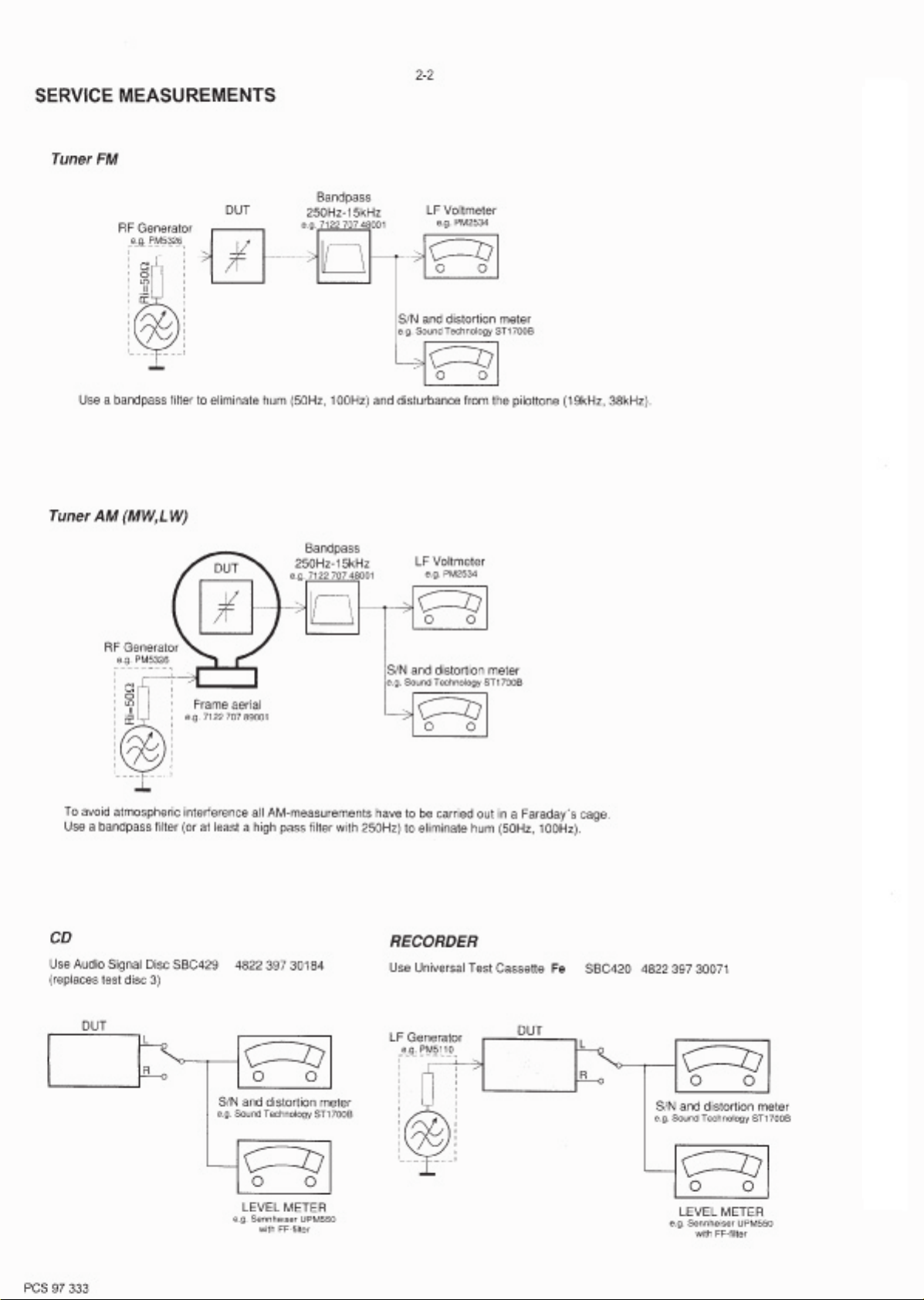
TECHNICAL SPECIFICATIONS
2-1
GENERAL
Mains voltage -/00 : 220 - 230 V
-/17 : 120v
Mains frequency -/00 : 50 Hz
-/17 : 60 Hz
Battery mains : 4.5 V
Power consumption max. : 17 W
standby : 3.4 W
Dimension (W x H x D) : 170 x 190 x 190 mm
Weight : 2.1 Kg
AMPLIFIER
Output power mains : 2 x 0.8 W
Speaker impedance : 2 x 8 ohm
Frequency response : 100 Hz - 10 kHz (±4dB)
TUNER - FM SECTION
Tuning range : 87.5 - 108 MHz
IF frequency : 10.7 MHz ± 0.3 MHz
Sensitivity : 3 µV at 26dB S/N
Selectivity : 24 dB at 300kHz
IF rejection : 55 dB
Image rejection : 26 dB
TUNER - AM SECTION
Tuning range MW : 526.5 – 1606.5 kHz
-/17 : 520 - 1722 kHz
IF frequency : 468 kHz ± 3 kHz
Sensitivity MW : 69 dBµV/m at 26dB S/N
Selectivity M W : 20 dB
IF rejection MW : 28 dB
Image rejection MW : 32 dB
COMPACT DISC
Frequency response : 125 Hz - 10 kHz
S/N ratio : 60 dB
Channel difference 1 kHz : 2 dB
Channel crosstalk 1 kHz : 40 dB
Laser wavelength : 780 ± 20 nm
Laser light power : < 0.5 mW
SERVICE TOOLS
Audio signal disc SBC 429.......................................................................4822 397 30184
Playability test disc SBC 444
Test disc 5 (disc without errors ) +
Test disc 5A (disc with dropout errors, black spots and fingerprints)
SBC 426/426A.....................................................................4822 397 30096
Burn in test disc (65 min. 1kHz signal at -30 dB level without “pause”)
Universal test cassette Fe SBC 420........................................................4822 397 30071
...................................................................4822 397 30245
.....4822 397 30155
PCS 107 249
Page 4
Page 5

CONNECTIONS AND CONTROLS
3-1
24 hours.
- sets the day for weekend sleeper activation.
- stops the active buzzer, radio or CD alarms for
- opens/ closes CD door.
- tunes to a radio station.
%SET DAY
^24 HR RESET
CONTROLS
•CD PLAYER
1STOP 9
&LIFT TO OPEN
*TUNING
- stops CD playback;
- stops sleep function in CD mode;
- stops the active CD alarm for 24 hours.
2PLAY/ PAUSE 2;
- aerial to improve FM reception.
(Pigtail
)Mains lead
- starts/ pauses CD playback.
passage.
- skips CD tracks/ searches for a particular
3SEARCH ∞, §
- for AC mains supply.
INSTALLATION
The type plate is located on the bottom of the
set.
CAUTION
Use of controls or adjustments or performance of
procedures other than herein may result in hazardous
radiation exposure or other unsafe operation.
BRIGHTNESS CONTROL
illumination;
- changes the brightness of the display
- switches off the alarm for a 9 minute period;
- activates and adjusts the sleep time.
•GENERAL
4SLEEP
5REPEAT ALARM/
^
- stops sleep function in CD, buzzer or radio mode.
6WEEKEND-SLEEPER
%
2
M
R
LA
MODE/OFF
A
Y
A
D
T
SE
Mains Supply and Demo mode
set.
- deactivates alarm 1 and/ or 2 for the weekend.
- shows the clock/ alarm time and status of the
7Display
8
2
E
M
U
L
O
V
plate on the bottom of the set, corresponds to your
local mains supply. If it does not, consult your
1 Check if the power voltage, shown on the type
dealer or service centre.
2 Connect the mains plug into the wall socket. The
- sets/ reviews/ switches off alarm 1 or 2.
8ALARM 1 MODE/ OFF or ALARM 2 MODE/ OFF
- switches the radio on/ off;
•RADIO
9ON/ OFF
#$@
continuously.
mains supply is now switched on and the display
will show the PHILIPS demo mode.
™ PH..IL..IPSscrolls across the display
• Press any control (with the exception of
- stops sleep function in radio mode;
- stops the active radio alarm for 24 hours.
- selects the radio waveband.
0FM/ AM (MW)
!
to exit the demo mode.
supply, withdraw the mains plug from the wall
REPEAT ALARM/ BRIGHTNESS CONTROL on the set)
•SETTING TIMES
!ALARM 1, ALARM 2, TIME
socket.
3 To disconnect the set completely from the mains
- sets the respective alarm or clock time
Standby power consumption (clock mode)......3 W
volume level for alarm 1 or 2;
- adjusts clock/ alarm times;
- adjusts the gentle wake minimum and maximum
- selects a CD wake up track for alarm 1 or 2.
@7, 8
- adjusts the sound level.
#VOLUME $, 3
$Frequency indicator
waveband
- shows the radio frequency of your selected
3 2 1
()*&&
z
z
h
RADIO
ON
9
H
k
M
0
8
0
0
6
1
1
•
4
0
1
•
8
9
•
3
9
•
8
8
M
F
OFF
2
M
T
R
A
E
0
0
2
1
0
5
8
0
3
6
0
3
5
W
M
FM
AM
L
A
S
M
R
A
L
A
-
E
M
E
M
I
T
1
I
M
T
R
A
L
A
0
PM
L
RO
M
P
R
TO
CONT
A
S
L
A
T
A
BRIGHTNESS
E
USE
P
A
P
E
/
Y
O
I
D
K RA
C
O
CL
C
IS
D
T
AC
MP
O
C
0
95
J3
A
R
PLA
H
C
R
A
E
S
SLEEPER
WEEKEND-
P
EE
L
S
IOIIOIOO
O
O
IO
547
I
6
MODE/OFF
ALARM 1
Z
FM
O
I
D
A
R
P
E
E
L
S
Z
1
8
PCS 107 250
Page 6

INSTRUCTIONS FOR USE
SETTING THE ALARM OPTIONS
General
Two different alarm times, ALARM 1or 2 can be set
in the CD, radio or buzzer modes. This can be useful
time functions correctly!
when for example you need to be woken up at a
different time during the week and at the weekend.
- Remember to first set the DAY, clock and alarm
- Make sure your selected alarm symbol is shown.
Viewing the Alarm Mode Options
1 Select your choice of alarm mode by pressing
gentle wake alarm
gentle wake alarm
CD mode with CD and a track number
(buzzer) k AL, or
(radio) m tu, or
– Followed by the 3 different alarms:
ALARM 1 or ALARM 2 MODE/ OFF once or more
to find your respective mode.
– H1:16 – default maximum volume level for
™ The alarm mode display sequence is shown:
– Lo:00 – default volume level for start of
3-2
1-99.
respective modes.
2 Read the following chapters to adjust or select the
Adjusting the Gentle Wake Volume
A sure way of getting up in the mornings, the gentle
wake volume for the alarm begins from gentle
volume e.g Lo:00 (low) and gradually increases to a
higher volume e.g. H1:11.
The default volume range is Lo:00 and H1:16. If
or ALARM 2 MODE/ OFF once.
you wish to change the default volume for the buzzer,
radio or CD alarm:
1 In the standby mode, press ALARM 1 MODE/ OFF
more to adjust the starting volume of your alarm.
ALARM 1 MODE/ OFF or ALARM 2 MODE/ OFF
again to change to the H1:16 display.
2 As soon as Lo:00appears, press 7or 8once or
3 To set the maximum volume for your alarm, press
reach the desired volume level (10-32).
4 As soon as H1:16appears, press 7or 8until you
Notes:
• The H1 volume is always greater or equal to the
track(s).
previous tracks.
Selecting a different track during playback
the beginning of the current track.
The track number appears briefly in the display when
you press SEARCH ∞ or § to skip tracks.
• Press SEARCH § once or more to skip to the next
• Press SEARCH ∞ more than once to skip to
• Press SEARCH ∞ once and playback will return to
SETTING THE DAY
Setting the day enables you to set the WEEKEND-
SLEEPER function. If you attempt to use the
WEEKEND-SLEEPER prior to setting the day
(Monday to Sunday, 1-7) will show briefly in
the display to remind you to set the day first.
1 Press SET DAY.
2 While the day display is shown, pressSET DAY
SEARCH ∞ or §.
™ The CD is played at high speed and low volume;
Finding a passage within a track
1 During playback, press and hold down
again once or more to select the day numbered
from dAY 1-7 (Monday-Sunday):
™ The display will revert to show the clock time.
CD PLAYBACK
RADIO
the display will show Cd: and your current
track number.
LIFT TO OPEN.
1 To open the CD door, lift at the edge marked
resumes.
the passage you want.
™ Normal CD playback and standby clock time
2 Release SEARCH ∞ or § when you recognize
close the door.
2 Insert a CD with the printed side facing up, and
RADIO
CD
number of tracks are shown, followed by the
™ The CD indicator , Cd:-- and the total
3 Press PLAY/ PAUSE 2;to start playback.
time , and the last selected
™ tuis displayed briefly followed by the clock
1 Press ON/ OFF to switch on the radio.
first track number before returning to clock time.
door/ open the CD door during playback.
– door is shown if you have not closed the CD
waveband.
inserted incorrectly.
– noCd is shown if no CD has been inserted/
station.
3 Adjust the sound using VOLUME $or 3.
4 Adjust the TUNING wheel to tune to a radio
To improve reception:
FM: Extend pigtail at the back of the set fully for
optimum reception.
2 Press FM/ AM if you wish to change waveband.
the set.
– nFCd is shown if the CD-R(W) is non-finalized
– Err indicates a general error in operation of
™ The display returns to clock time.
4 Adjust the sound with VOLUME $or 3.
AM (MW): uses a built-in aerial. Direct the antenna
CD
returning to clock time. flashes during
5 To interrupt, press PLAY/ PAUSE 2;.
• The current track number shows briefly before
RADIO
the display.
™ and the waveband disappear from
by adjusting the position of your set.
5 Press ON/ OFF to switch off the radio.
playback.
pause.
™ The display returns to clock time.
7 Press STOP 9to stop playback.
6 Press PLAY/ PAUSE 2; again to resume
MEMORY BACKUP
The memory backup conveniently allows your day,
PCS 107 251
will show the PHILIPS demo mode and you will
alarm and clock time settings to be stored for up to 3
need to re-enter the day, alarm and clock times.
minutes when there is a mains interruption e.g.
AC mains failure.
The complete CD clock radio and illumination will be
switched off. As soon as the mains supply returns, the
display will indicate the correct time.
• If mains supply returns after 3 minutes, the display
BASIC FEATURES
or more.
Illumination brightness
™ The brightness of the display will change in this
• Press REPEAT ALARM/ BRIGHTNES CONTROL once
sequence:
LOW ? MEDIUM ? BRIGHT ? LOW...
Volume
Press VOLUME $ or 3to adjust the volume level.
SETTING THE CLOCK AND ALARM TIMES
0-32.
The volume level UO: is indicated as a number from
the respective clock or alarm time display flashes.
and minutes.
decreases rapidly and continuously from minutes to
hours. Release 7or 8when you have reached the
correct setting.
minute, press 7or 8briefly and repeatedly.
The time is displayed using the 24 hour clock.
1 PressTIME, ALARM 1 or ALARM 2 briefly until
2 Press and hold down 7, 8to adjust both the hours
• By pressing 7or 8respectively, the time increases/
• If you need to adjust the time slowly, minute by
3 Press TIME, ALARM 1 orALARM 2 to confirm
your respective time setting.
Page 7

INSTRUCTIONS FOR USE
long time, withdraw the power plug from the wall
outlet.
sand or excessive heat caused by heating
equipment or direct sunlight.
chamois leather. Do not use any cleaning agents
containing alcohol, ammonia, benzene or abrasives
MAINTENANCE
General (See figure 6)
• If you do not intend to use the CD clock radio for a
• Do not expose the set or CDs to humidity, rain,
Z
as these may harm the housing.
• To clean the set, use a soft, slightly dampened
3-3
can cause condensation to form and the lens of
your CD player to cloud over. Playing a CD is then
not possible. Do not attempt to clean the lens but
leave the set in a warm environment until the
moisture evaporates.
compartment dust-free. To clean, dust the
compartment with a soft dry cloth.
spindle while lifting the CD. Always pick up the CD
CD player and CD handling
• The lens of the CD player should never be touched!
• Sudden changes in the surrounding temperature
• Always shut the CD door to keep the CD
by the edge and replace the CD in its box after use
• To take a CD out of its box, press the centre
to avoid scratching and dust.
centre towards the edge using a soft, lint-free
cloth. Do not use cleaning agents as they may
• To clean the CD, wipe in a straight line from the
damage the disc.
• Never write on a CD or attach any stickers to it.
Environmental information
All unnecessary packaging material has been omitted
to make the packaging easy to separate into three
materials: cardboard (box), expandable polystyrene
(buffer), polyethylene (bags, protective foam).
SLEEP
Your set consists of materials which can be recycled if
disassembled by a specialized company. Please
observe local regulations on the disposal of packing
materials and old equipment.
disappears from the display.
Z
appears for one or both alarms.
step 1 until Z
WEEKEND-SLEEPER
This feature deactivates the alarm every Saturday and
Sunday and resumes the alarm function Monday to
Friday. Make sure, however, that you have set the day
first.
• See chapter on SETTING THE DAY.
1 Press WEEKEND-SLEEPER once or more until Z
– inserted a CD incorrectly;
– inserted a damaged CD;
– forgotten to insert any CD;
– not closed the CD door properly.
SWITCHING OFF THE ALARM
There are three ways of switching off the alarm.
Unless you cancel the alarm completely, the
See figure 4.
2 To cancel the weekend-sleeper function repeat
24 HOUR ALARM RESET will be automatically
SLEEP
24 HOUR ALARM RESET
selected after 59 minutes, from the time your alarm
time first goes off.
If you want the alarm mode to be stopped
switch on the respective mode.
About Sleep
The CD clock radio has a built-in sleep timer which
enables the set to be automatically switched off
during radio or CD playback after a set period of time.
There are four sleep times before the set turns itself
off:
10, 30, 60, 90 minutes and off.
The sleep function does not affect the operation of
your alarm settings.
Setting Sleep
1 Press PLAY/ PAUSE2; (CD) or ON/ OFF (radio) to
CD alarms
selected alarm:
immediately but also wish to retain the same alarm
a 24 HR RESET to switch off the buzzer, radio or
setting for the following day:
• Press from 3 possible options according to your
reset activation.
b STOP 9 CD alarm only
c ON/ OFF radio alarm only.
™ You will hear a beep tone confirming 24 hour
disc first.
• For the CD mode, make sure you have inserted a
CANCELING THE ALARM COMPLETELY
To cancel the set alarm time before it goes off, or
during the alarm call:
• Press ALARM 1 MODE/ OFF or ALARM 2 MODE/
more until the desired sleep time is shown.
2 Select your sleep time by pressing SLEEP once or
OFF once or more until the selected alarm indicator
disappears from the display.
disappears from the display
See figure 5
3 To cancel the sleep function you can either:
– press SLEEP once or more untily
will also hear a beep tone confirming the alarm
™ If you cancel the alarm during the alarm call, you
– press STOP 9 (CD only)
– press REPEAT ALARM/ BRIGHTNESS CONTROL
– press ON/ OFF (radio only).
has been cancelled.
press REPEAT ALARM/ BRIGHTNESS CONTROL.
REPEAT ALARM
This will repeat your alarm call at 9-minute intervals.
• During the alarm call,
• Repeat if desired up to an hour.
Notes:
• The selected alarm mode k, m , or indicators will
flash throughout the repeat alarm duration.
resumes at the point interrupted by the repeat alarm.
to an hour unless you cancel/ reset the alarm.
• If you are using the CD alarm mode, CD playback
• During the CD alarm, CD playback continues for up
e.g.ii. Lo:12, H1:12
Lo volume: e.g.i. Lo:15, H1:19
• The starting volume is Lo:00, with a possible
low volume range 00-32, and the maximum
volume is H1:32, with a possible high volume
range10-32.
normal CD and radio playback volume level.
• The gentle wake volume settings do not affect
cancels the alarm completely.
range during the active alarm call as pressing
ALARM 1 MODE/ OFF or ALARM 2 MODE/ OFF
• It is not possible to review the gentle wake volume
• During the alarm call, if you press 7or 8the high
volume stops increasing immediately.
OFF repeatedly until the (buzzer) k AL or
(radio) m tu display is shown.
Selecting Buzzer or Radio Alarm
• Press ALARM 1 MODE/ OFF or ALARM 2 MODE/
Note:
If you have selected the radio alarm m tu, make sure
you have tuned properly to a station.
ALARM 2 MODE/ OFF repeatedly until the CD and
track number display is shown.
CD Alarm Mode: Selecting a CD track
You can program and select a CD track number
between 1-99, when the set is in the standby or radio
playback mode.
However, if the track number programmed does not
exist on your CD, the CD will start playback from the
first track during the alarm call.
1 Insert a CD into the CD compartment.
See figure 3.
2 Press ALARM 1 MODE/ OFF or
3 As soon as the CD alarm display appears,
press 7or 8until the desired track number is
shown.
™ The display returns to standby clock time.
again repeatedly until the CD alarm display is
shown.
ALARM 1 MODE/ OFF or ALARM 2 MODE/ OFF
4 To review your programmed track number, press
the CD alarm if you have:
Note:
• The buzzer alarm option will automatically replace
PCS 107 252
Page 8

INSTRUCTIONS FOR USE
3-4
TROUBLESHOOTING
If a fault occurs, first check the points listed below before taking the set for repair.
PCS 107 253
•RADIO
Occasional crackling sound during
FM broadcast
Weak signal
- Extend pigtail fully
Continuous crackling/
hiss disturbance during AM (MW) broadcast
Electrical interference from TVs, computers,
fluorescent lamps, etc.
- Move set away from other electrical equipment
•ALARM
The alarm does not function
Problem
Possible Cause
- Remedy
No sound
Volume not adjusted
- Adjust the volume
If you are unable to remedy a problem by following these hints, consult your dealer or service centre
WARNING:
Do not open the set as there is a risk of electric shock!
Under no circumstances should you try to repair the set yourself, as this will invalidate the guarantee.
No reaction to any operation of the buttons
reconnect the set after 5 minutes
Electrostatic discharge
- Disconnect the set from the power supply and
•CD PLAYER
TIMES
Alarm time not set
- See chapter on SETTING THE CLOCK AND ALARM
Alarm mode not selected
- See chapter on SETTING THE ALARM OPTIONS
CD playback does not work
CD badly scratched or dirty
- Replace/ clean CD
Laser lens steamed up
- Wait until lens has acclimatized
Volume too low for radio/ CD/ buzzer alarm mode.
- See chapter on Adjusting the Gentle wake volume
•WEEKEND-SLEEPER
WEEKEND-SLEEPER does not function
Day selection not set/ incorrect
- See chapter on SETTING THE DAY
WEEKEND-SLEEPER not set
- Set WEEKEND-SLEEPER
This product complies with the radio interference
requirements of the European Union.
Laser lens dirty
- Clean lens by playing a CD lens cleaning disc
CD-R(W) is non-finalized
- Use a finalized CD-R(W)
Page 9

DISASSEMBLY DIAGRAM
A. To remove Rear Cabinet
B. To remove Speaker Frame
C. To remove CD Tray and Middle Bracket
D. To remove Middle Bracket
E. To remove Main Board
F. To remove Repeat Alarm Key
4-1 4-1
PCS 107 254
Page 10

CD SERVICE TEST PROGRAM
STOP button pressed in any step returns
*
to begin of Service Testprogram.
To leave Service Testprogram switch mode switch
*
to off-position.
Door switch is ignored Æ CD door can be opened.
*
Volume up/down buttons function independentely
*
of the service testprogram.
4-2 4-2
For entering the Factory and Service mode keep BAND and NEXT keys pressed while power up (plug-in) the set.
The set will enter CD repeat all mode.
For entering the Factory and Service mode keep BAND and PREV keys pressed while power up (plug-in) the set.
The set will enter CD repeat one mode.
DISPLAY TEST
ALARM 1 button
N
pressed?
Display shows all
segments and flags.
see figure 1
To enter Service
Testprogramm hold
BAND & PLAY buttons
depressed while power
up the set.
Display shows
version number
of the µP - software.
N
r001
PLAY button
pressed?
Y
Display shows
01
BUZZER TEST
SET DAY button
N
pressed?
Y
Y
Display shows
AL
Buzzer is turn on.
CD TEST
Slide servo, Radial servo, Focus servo, Disc motor
and Laser are switched off.
Mute is switched on via decoder IC.
CD SERVO TEST
SLIDE test DISC MOTOR test
fig. 1
N
STOP button
pressed?
Y
N
STOP button
pressed?
Y
N N N N N
SLEEP button
pressed?
FOCUS search
Display shows
noFo
objective moves up&down
disc motor for 160ms "on"
FOCUS found?
Display shows
Y Y Y Y Y
Y
outside as long as
N
NEXT button
pressed?
Slide moves
button is held
depressed.
PREV. button
pressed?
Slide moves
inside as long as
button is held
depressed.
24 HR RESET
button pressed?
Disc motor turns
counter clockwise
as long as button
is held depressed.
(brake)
SET DAY button
pressed?
Disc motor turns
clockwise
as long as button
is held depressed.
(accelerate)
Fo
disc motor turns.
STOP button
pressed?
N
Y
WEEKEND SLEEPER
button pressed?
Y
Enable
CD-RW mode
and shows
FM flag.
N
PCS 107 255
Page 11

4-3 4-3
Abbreviations and Pin-description of CD Ics
Abbreviations and Pin-description of CD Ics
SERVO PROCESSOR SAA7325H
SYMBOL PIN DESCRIPTION
HFREF 1 comparator common mode input
HFIN 2 comparator signal input
ISLICE 3 current feedback output from data slicer
V
SSA1
V
DDA1
I
ref
V
RIN
D1 8 unipolar current input (central diode signal input)
D2 9 unipolar current input (central diode signal input)
D3 10 unipolar current input (central diode signal input)
D4 11 unipolar current input (central diode signal input)
R1 12 unipolar current input (satellite diode signal input)
R2 13 unipolar current input (satellite diode signal input)
V
SSA2
CROUT 15 crystal/resonator output
CRIN 16 crystal/resonator input
V
DDA2
LN 18 DAC left channel differential output - negative
LP 19 DAC left channel differential output - positive
V
neg
V
pos
RN 22 DAC right channel differential output - negative
RP 23 DAC right channel differential output - positive
SELPLL 24 selects whether internal clock multiplier PLL is used
TEST1 25 test control input 1; this pin should be tied LOW
CL16 26 16.9344 MHz system clock output
DATA 27 serial d4(1)ata output (3-state)
WCLK 28 word clock output (3-state)
SCLK 29 serial bit clock output (3-state)
EF 30 C2 error flag output (3-state)
TEST2 31 test control input 2; this pin should be tied LOW
KILL 32 kill output (programmable; open-drain)
V
SSD1
V2/V3 34 versatile I/O: input versatile pin 2 or output versatile pin 3 (open-drain)
WCLI 35 word clock iutput (for data loopback to DAC)
SDI 36 serial data input (for data loopback to DAC)
SCLI 37 serial bit clock input (for data loopback to DAC)
RESET 38 power-on reset input (active LOW)
SDA 39 microcontroller interface data I/O line (open-drain output)
SCL 40 microcontroller interface clock line input
(1)
4
(1)
5
analog ground 1
analog supply voltage 1
6 reference current output pin
7 reference voltage for servo ADC's
(1)
14
17
(1)
analog ground 2
analog supply voltage 2
20 DAC negative reference input
21 DAC positive reference input
(1)
33
digital ground 2
SERVO PROCESSOR SAA7325H
SYMBOL PIN DESCRIPTION
RAB 41 microcontroller interface R/W and load control line input (4-wire bus mode)
SILD 42 microcontroller interface R/W and load control line input (4-wire bus mode)
STATUS 43 servo interrupt request line/decoder status register output (open-drain)
TEST3 44 test control input 3; this pin should be tied LOW
RCK 45 subcode clock input
SUB 46 P-to-W subcode bits output (3-state)
SFSY 47 subcode frame sync output (3-state)
SBSY 48 subcode block sync output (3-state)
CL11/4 49 11.2896 MHz or 4.2336 MHz (for microcontroller) clock output
V
SSD2
DOBM 51 bi-phase mark output (externally buffered; 3-state)
V
DDD1(P)
CFLG 53 correction flag output (open-drain)
RA 54 radial actuator output
FO 55 focus actuator output
SL 56 sledge control output
V
DDD2(C)
V
SSD3
MOTO1 59 motor output 1; versatile (3-state)
MOTO2 60 motor output 2; versatile (3-state)
V4 61 versatile output pin 4
V5 62 versatile output pin 5
V1 63 versatile intput pin 1
LDON 64 laser drive on output (open-drain)
Note : All supply pins must be connected to the same external power supply voltage.
50
52
57
58
(1)
(1)
(1)
(1)
digital ground 3
digital supply voltage 2 for periphery
digital supply voltage 3 for core
digital ground 4
PCS 99 458
Page 12

BLOCK DIAGRAM
5-1 5-1
PCS 107 256
Page 13

WIRING DIAGRAM
6-1 6-1
PCS 107 257
Page 14

MAIN BOARD (Part 1) - CIRCUIT DIAGRAM
7-1 7-1
PCS 107 258
Page 15

7-2 7-2
MAIN BOARD (Component Side View) - LAYOUT DIAGRAM
CD KEYBOARD - LAYOUT DIAGRAM
KEYBOARD - LAYOUT DIAGRAM
LED BOARD - LAYOUT DIAGRAM
KEYBOARD (TOP) - LAYOUT DIAGRAM
PCS 107 259
Page 16

MAIN BOARD (Part 2) - CIRCUIT DIAGRAM
8-1 8-1
PCS 107 260
Page 17

8-2 8-2
MAIN BOARD (Copper Side View) - LAYOUT DIAGRAM
POWER BOARD - LAYOUT DIAGRAM
CD DOOR SWITCH - LAYOUT DIAGRAM
PCS 107 261
Page 18

TUNER BOARD ATM5 - CIRCUIT DIAGRAM
9-1 9-1
1 2 3 4 5 11 12
A
A
9018
B
C
D
E
F
1104
9020
9021
5111
2116
2119
3114
*
FERRITE ONLYFRAME ONLY
5102
USA OSC
15n
22n
15n
22n
ON OFF
20p
18p2108
FM-OSC
Provisional
AM-OSC
FRAME LOOP
T013
B
G
FM : 87.0(+/-0.5) ... 108.5(+/-0.5) MHz
AM : 520(+/-10) ... 1730(+/-20) KHz
3114
*
2110
T012
T003
6101
T002
8p2
Provisional
1104
XH-S
6102
BAS216
BAS216
2109
820R
2p2
3 4
2
1
7
9020
1
2
9021
5102
FERRITE BAR
USA
2108
5105
RED
8
5100
OSC
20p
6
6
2102
5104
AM-RF
2103
ORANGE
1
PAD1
PAD2
1
1001
1
47p
100MHZ
Vp
VSTABA
VSTABB
10u
T001
5111
78
FM-RF
2101
34
2
1
AM-RF
4n7
1
17 RFGND
23 FM-OSC
25 VP
19 RIPPLE
12 VSTABA
6 IFGND
24 AM-OSC
18 AM-RFI
C
24p
2105
7101
TEA5711T
NC
VSTABB8
6
3T5
5101
16
21
FM-RFI
FM
FRONTFMMIXFMIF1
STABILIZER
AM
FRONT
5106WHITE
7M4A545N
78
FM-RFO
FM
OSC
AM
OSC
AM
MIX
34
2
1
VSTABA
FM-MIX
AM-MIX
6 7 8 9 10
5107a
SFE10.7MS3
180KHz
3
1
O
I
G
2
VSTABA
11
13
FM-IF1I
FM-IF1O
AGC
AM
IF
AM-IF1I10AM-IF2I|O
15
14
7M4A522A
6
5107b
SFE10.7MS2
230KHz
1I3
G
VSTABB
9
7
FM-IF2I
FM
IF2FMDET
AM FM
AM/FM
INDIC CONV
IND
AGC|AFC
26
20
5108BLACK
34
2
1
78
VSTABB
O
2
5
FM-DEM
AM
DET
2104
CDA10.7MC1
PHASE
SWITCH
AFO
28
10u
5107c
DET
PILOT
PRESENCE
SELECTOR
PILFIL
4
T010
4u7
2115
2121
31
LPF-M|S
CTRL
V-I
MPXI32MUTE
29
2113
2114
2K2
3104
1u
2122
470n
27
VCO|AM-FM-S
VCO/
DIV
SDS/
DET
MUTE/
MATRIX
MONO/
STEREO
SUBGND
22
220n
2120
1u
330p
3113
500R
3101
3102
150K
7102
BC847B
68K
3AF-RO
2AF-LO
30ST-LED
AM-RF
AM-OSC
3
2119
2116
T006
3121
*
*
1
3
22K
3120
2118
1u
2117
1u
C4 AMrf
C2 FMrf
2106
WF420
AM-ANT
AM-OSC
100K
2
3110
100K
3109
100K
1
Vp
PVC TOP VIEW
C1 FMosc
FM-ANT
MT16MT2
FM-OSC
5
T009
T007
T004
T005
T008
3108
2112
C3 AMosc
All SMD Transistors
B
E
Top View from
Solder Side
1110
FE-BT-VK-N
1
2
3
4
5
33R
BAND
47u
7mm PACK
3
2
1
BOTTOM VIEW
FM-RF
2
FM-OSC
4
L
GND
R
B+
+FM
AM
FM
C
+FM
Lo
Hi
4
6
A
B
C
D
E
F
G
1001 A4
1104 E3
1110 B11
2101 A4
2102 A4
2103 D4
2104 G7
2105 A5
2106 F10
2108 C3
2109 C3
2110 D2
2112 D11
2113 F8
2114 G8
2115 G7
2116 C9
2117 C10
2118 B10
2119 C9
2120 G8
2121 A8
2122 B8
3101 A9
3102 B9
3104 A8
3108 D11
3109 C10
3110 C10
3113 G9
3114 C2
3120 A10
3121 A9
5100 A3
5101 A5
5102 G3
5104 C4
5105 D3
5106 F5
5107a A6
5107b A7
5107c A7
5108 F7
5111 E4
6101 A2
6102 A3
7101 B5
7102 A9
9018 A2
9020 E3
9021 F3
T001 E4
T002 B3
T003 A3
T004 B11
T005 C11
T006 E9
T007 B11
T008 C11
T009 B11
T010 F8
T012 G2
T013 F2
PCS 107 262
1 2 3
4 5 6 7 8 9 10
11 12
Page 19

TUNER BOARD ATM5 - LAYOUT DIAGRAM
FM/MW versions
9-2 9-2
TUNER ADJUSTMENT TABLE
Input FrequencyWaverange Input Set tuned to Adjust Measure on Scope / Counter
1001 E1 2122 D6
1104 A2 3101 E6
1110 F6 5101 C1
2103 D2 5102 B3
2104 D1 5104 D5
2105 C2 5105 C6
2106 C3 5106 G2
2108 B5 5107a F3
2109 B5 5107b F4
2110 B6 5107c F4
2112 E5 5108 G3
2113 D6 5111 B1
2115 F5 5112 B2
2117 F5 9018 F1
2118 G6 9020 A2
2120 C6 9021 A1
2121 E6 9027 D5
OSCILLATOR
FM
87,5 - 108 MHz
MW
525 - 1607 kHz
(530 - 1710 kHz)
FM - RF
1)
87,35 MHz
108,25 MHz
512 kHz
(520 kHz)
1635 kHz
(1730 kHz)
A
D f = ±500kHz
VRF = 100µV
C
D f = ±30kHz
VRF = 100µV
lower band end
upper band end
lower band end
upper band end
5104
2106 C1
5105
2106 C3
or
1 2
or
1 2
f
o
f
o
2101 F6 3121 F1
2102 E7 6101 G7
2114 E3 6102 G7
2116 F3 7101 E5
2119 G3 7102 F2
3102 E1 9010 F7
3104 E2 9011 E7
3108 E3 9012 F3
3109 F2 9013 F1
3110 G2 9015 E4
3113 D2 9017 E6
3114 D4 9026 E3
3120 F2 9028 G6
FM
87,5 - 108 MHz
87,5 MHz
108 MHz
A
D f = ±500kHz
VRF = 10µV
87,5 MHz
108 MHz 2106 C2
VCO
A
FM 98 MHz 98 MHz
continuous
wave
VRF = 1 mV
AM - IF
IC 7101
AM
468 kHz
connect pin 24 of
IC 7101 (AM Osc)
with short wire to
ground
C
D f = ±15kHz
VRF = 10mV
IC 7101
see
remark
2)
AM -RF
B
560 kHz
MW
10
220R
14
220R
100nF
100nF
5101
3101
5106
5108
5111560 kHz
or
1
7101
pin 30
2k2
3
or
1 2
or
1 2
2
4k7
V
max.
152 ±1 kHz
cc
max.
f
o
symmetric
max.
repeat
1500 kHz
1)
for USA /17
2)
RC-network serves for damping the IF-filter while adjusting the other one.
D f = ±30kHz
VRF as low as
possible
1500 kHz
2106 C4
symmetric
PCS 107 263
Page 20

CD99 DA11 - LAYOUT DIAGRAM
10-1 10-1
A
B
C
D
E
F
G
H
1 2 3 4 5
CD99 Board component side view
2840
8
1801
7809
3863
1 6
16 9
1
15
1824
6 2
1810
1 3
1821
2857
2823
5803
2846
17
2851
1823
6 2
16
3855
7808
1
2836
This assembly drawing shows a summary
of all possible versions.
For components used in a specific version
see schematic diagram respectively partslist.
2855
2854
5802
3
1
8
4
6
3750
3751
7
2817
2 14
1
1800
9
8
1 2 3 4 5
F4
D3
3703 B5
3704 A2
3705 A3
3728 E5
3745 B3
3750 B2
3751 B2
3757 B3
3788 C5
3800 F1
3801 G2
3802 G2
3803 G1
3804 G1
3805 G1
3806 G1
3807 F1
3808 F2
3809 F1
3810 E1
3811 D1
3812 D1
3813 D2
3814 D1
3815 D1
3816 D1
3817 C2
3818 C1
3819 D1
3820 C1
3821 C1
3822 C1
3823 C2
3824 C2
3825 C2
3826 D3
3827 D2
3828 E4
3829 D5
3830 D4
3831 F5
3832 F5
3834 D5
3835 C4
3836 C5
3837 C4
3838 C4
3839 C4
3840 B4
3841 B4
3842 A3
3843 A3
3844 A3
3845 C3
3846 A3
3847 B3
3848 B2
3849 H4
3850
3851 B3
3852 B2
3853 H3
3854 H3
3855 G5
3856 B3
3857 B3
3858 A5
3859 C2
3860 B2
3861 B2
3862 B2
3863 A4
3864 E1
3865 E1
3867 E4
3868 E4
3869 E4
3870 F4
3871 E4
3872 F5
3873
3874 E4
3875 F3
1800 F2
1801 A5
1810 D3
1821 E5
1822 A2
1823 G5
A
B
C
D
E
F
G
H
1824 D5
2701 B4
2702 A2
2703 A2
2704 A2
2801 F1
2802 E1
2803 D2
2804 D2
2805 D2
2806 E1
2807 D2
2808 D2
2809 D1
2810 C1
2811 C2
2812 C1
2813 C2
2814 D2
2815 C2
2816 C2
2817 D2
2818 D2
2819 E4
2820 E3
2821 D4
2822 D4
2823 E4
2824 D4
2825 D4
2826 F5
2827 C5
2828 C4
2829 A4
2830 B3
2831 B3
2832 B2
2833 H4
2834 B2
2835 H3
2836 G5
2837 B2
2838 B5
2839 A5
2840 A4
2841 E2
2842 C1
2843 E4
2844 E3
2845 E4
2846 E4
2847 F5
2848
2849 F3
2850 F4
2851 G4
2852 F5
2853 E5
2854 F3
2855 E3
2856 D5
2857 E5
2860 E3
2861 E2
2862 E2
2863 D2
2864 D2
2865 D2
2869 F1
2870 E3
2871 E3
2872 E3
2873 D3
2874 D3
2875
3701 B4
3702 B4
1
1822
3
2842
2802
3810
15
2801
99-05-21
3415.4
CD99 Layout stage .4 990817
H4
E4
3876 F4
3877 F4
3878 F4
3879 F5
3880 F5
3881 E5
3882 F4
3883 F3
3884 E3
3885 B5
3886 C5
3887 B5
3888 C5
3889 D5
3890 D2
3891 E2
3892 D2
3893 D2
3894 E3
3895 E2
3896 E2
3897 D2
3898 D2
3899 D2
3900 D4
4801 E5
4802 F2
4804 D4
4805 E4
4806 D5
4807 E2
4808 D5
4809 D5
4810 B2
4812 B4
4813 B3
4814 B3
4815 A4
4823 C2
4824 B2
4828 B2
4831 B3
4832 B3
4838 C5
4845 D2
4847 E1
4848 B4
4850 G5
4853 F2
4856 F5
4857 B4
4859 B5
4863 C5
4865 A4
4866 B4
4872 F2
4877 H5
4881 G5
E2
4884
4885 G5
4886 G1
4888 F2
4889 G1
5802 A2
5803 E5
6877 F5
7800 C4
7802 C2
7803 F1
7804 G2
7807 D1
7808 G4
7809 A5
7810 F4
7875 F5
8401 H3
8402 H5
A
B
C
D
E
F
G
H
CD99 Board copper side view
99-05-21
3415.4
This assembly drawing shows a summary
of all possible versions.
For components used in a specific version
see schematic diagram respectively partslist.
A
B
C
D
E
F
G
H
CD99 Layout stage .4 990817
PCS 104 487
1 2 3 4 5
1 2 3 4 5
Page 21

CD99 DA11 - CIRCUIT DIAGRAM
10-2 10-2 10-2
1800 D1
1801 G1
2801 A2
2802 A3
2803 E4
2804 E4
2805 E4
2806 E4
2807 E4
2808 E4
2809 E6
2810 E6
2811 F7
2812 E8
1 2 3 4 5 6 7 8 9
CD Part (sheet 1)
Vdd_HCU
A
27K
3801
3805
150K
3
0,2V
27K
2
3803
0,2V
4K7
B
C
D
E
F
G
H
3804
Monitor
LDON
L
SANYO DA11
F
D
A
B
E
TRACK
FOCUS
side entry connector
1K
3802
+5V
L
comm. cath
C
-
SLIDE
+
INNERSW.
+
DISC
-
1 2 3 4 5 6 7 8 9 10 11 12 13 14 15
2813 E9
2814 E9
2815 E10
2816 F10
2817 D9
2818 D9
2819 B10
5V
7804-A
8
LM358D
4
L
1
680R
2,5V
3806
1K5
3807
2820 B10
2821 B11
2822 B11
2823 B11
2824 B11
2825 B12
2826 A13
47u
4R73800
3,3V
BC807-40
Laser power control
10K
3864
47n
2841
1800
1
B
2
E
3
F
4
D
5
6
C
7
A
8
M
9
10
L
11
L
12
T-
13
F+
14
T+
15
F-
1
2
3
Innersw
4
5
6
1801
EH-S
2801
33R
33R
3809
3808
3,9V
1,8V
7803
LASER
286947n
during Focus search
connect shielding
2827 C14
2828 C14
2829 G14
2830 F13
2831 G12
2832 F5
2833 F4
L
L
T = 1 s
2802
6,2V
FOCUS
6,1V
6,2V
TRACK
6,0V
6,1V
SLIDE
6,2V
6,5V
DISC
8401
5,9V
L
Monitor
LASER
2834 F5
2835 F4
2836 F4
2837 G5
2838 G4
2839 H4
2840 H4
2841 C1
2842 F7
2860 B5
2861 B5
2862 C5
2863 C5
2864 D5
2865 D5
2869 E2
2870 B5
2871 B5
2872 C5
2873 C5
2874 D5
2875 D5
3728 A10
3745 G12
3750 G11
3751 G11
3757 G5
3800 B2
3801 A1
3802 B1
3803 B1
3804 B1
3805 A1
3806 B2
3807 A2
3808 A2
3809 A2
3810 A3
3811 E4
3812 D5
3813 E5
3814 E5
3815 E5
3816 E5
3817 E7
3818 E6
3819 E6
3820 E7
3821 E7
3822 E7
3823 E8
3824 E9
3825 E9
3826 D10
3827 D9
3828 A10
3829 A11
3830 B12
3831 B14
3832 B14
3834 B14
3835 C14
3837 C14
3838 D14
3839 D14
3840 D15
3841 E14
3842 G14
3843 G14
3844 G13
3845 G12
3846 F10
3847 F6
3848 F5
3849 E5
3850 F5
3851 F6
3852 F5
3853 F5
3854 F5
3855 F4
3856 G6
3857 G5
3858 G5
3859 H5
3860 H5
3861 H5
3862 H5
3863 H4
3864 C1
3865 F7
3890 B4
3891 C4
3892 C4
3893 D4
3894 A5
3895 B5
3896 B5
3897 C5
3898 C5
3899 D5
7800 D12
7802-A E6
7802-B E5
7802-C E5
10 11 12 13 14
3828
3810
+5V
4R7
2808
150p
3855
PTH8
3863
3R3
A
7802-C
8K2
+t
8K2
3K9
2860
2861
2862
2863
2864
2865
3894
10K
560p
HF
1n5
HF
180p
HF
180p
HF
180p
HF
180p
HF
3812470K
3813
68K
Y
6
3849
56K
3850
Vref
+10V
3853
15K
3854
Vref
3857
68K
3858
Vref
+10V
3860 1K
3861
3862 1K
3895
10K
3896
10K
3897
10K
3898
10K
3899
10K
3K3
3814
47K3859
47K
3757
22K
D
D
2871 2870
2872
2873
2874
2875
3
3848
47K
3852
47K
220p
DA
220p
DA
220p
DA
220p
DA
220p
DA
220p
DA
4K7
3815
3816
15K
A4Y
7802-B
47n
M2
M1
0,9V 0,9V
2832
2834
2837
D
150p
D
270p
D
3856
68K
0,9V 0,9V
2809
33p
3847
82K
3851
56K
BC847C
7807
1,5V 0V
3818
5K6
7802-A
A1Y
3819
15K
HF-Amplifier
3817
47K
2810
2
33p
Vdd_HCU
of HCU
VCC
2842
HF
3820
18K
A11Y
7802-E
1u
3K3
3K3
10
3821
3822
33p
2811
HF
3865
+5V
1K
3V
0V
47u
3890
100K
3891
100K
3892
100K
3893
100K
82p
82p
7808
+
+
-
7809
+
+
-
2804
2807
27p
1
2
5
6
7
8
1
2
5
6
7
2805
2806 82p
FOCUS
10V
2836
47u
TRACK
SLIDE
2840
47u
100n
DISC
3811
1K
2833
2838
470p
2839
5
470p
2835
22n
2803 82p
HF
TDA7073A
+
16
14
_
13
12
_
10
+
9
16
+
14
_
13
12
_
10
+
9
VDD
TDA7073A
VDD
9
3823
3K3
7802-D
A8Y
2812
10p
R2 (CD10)
R1 (CD10)
D4 (CD10)
D3 (CD10)
D2 (CD10)
D1 (CD10)
2817
4u7
HF
2813
2n2
EYE-PATTERN
+3.3V
33R
3827
3824
1K
TB = 0.5m s/div
3728
47R
+3.3V
only for digital out versions
(Quartz used)
33p
2819
1810
8.46 MHz
D
47n
2818
L
27K
3826
HF
DA
HF
HF
47n
2814
22K
HF
LOW = CD_RW (high gain)
3825
2816 22n
800mVpp
L
HFIN
2815
LDON
47p
47R
2820
Innersw
16
15
14
13
12
11
10
33p
9
8
7
6
5
4
3
2
1
2821
D
CRIN
CROUT
VSSA2
R2
R1
D4
D3
D2
D1
VRIN
IREF
VDDA1
VSSA1
ISLICE
HFIN
HFREF
LDON
100n
VDDA2
+3servo
22K
17
TIMING
ADC
VREF GEN.
64
3846
DACLEFT_pos
DACLEFT_neg
2822
1n5
18LN19
LP
BITSTREAM DAC
FRONT
END
VERSATILE
INTERFACE
V1
V5
63
22K
3750
@ @
drive_recognition
7802-D E8
7802-E E7
7802-F F8
7803 B2
7804-A A1
7804-B C3
7807 E6
D
2823
220u
2824
47n
20
VNEG
PRE-
PROCESSING
CONTROL
FUNCTION
61V462
22K
3751
+3.3V
3829
21
VPOS
EFM
DEMOD
DIG.
PLL
MOTOR
CONTROL
MOTO2
60
M1M2
7808 E4
7809 G4
8401 H3
DACRIGHT_pos
DACRIGHT_neg
100R
2825
1n5
23
22
RP
RN
PROCESSOR
ADDR
VSSD3
MOTO1
58
59
2831
1u
D
AUDIO
SRAM
VDDD2C
+3.3V
24
SELPLL
3845 2R2
3745 10R
SL
D
4K7
3830
25
TEST1
SAA7325H
7800
OUTPUT
STAGES
SL
FO
56
26
CL16
55
RAFO
GNDA
27
DATA
SER. DATA
INTERFACE
ERROR
CORR.
RA
54
D
CFLG
53
2830
2826
47n
28
WCLK
PEAK
DET.
INTERF.
1u
+3.3V
EBU
VDDD1P
100R
29
5257
30
EF
SCLK
VERSAT.
KILL
INTERF.
SER. DATA
LOOPBACK
INTERF.
MICROCONTROLLER
SUBCODE
DOEM
51
3844
+3servo
for digital out: 33E
V
15
table for drive- and digital out recognition
stuffed resistor
3750
3751
3834
3835
+5V
D
31
TEST2
INTERFACE
PROCESSOR
VSSD2
50
D
Vref
EVM
3831
@
32
KILL
D
VSSD1
33
V2|V3
34
D
WCLI
35
D
SDI
36
D
SCLI
37
RESETn
38
SDA
39
SCL
40
RAB
41
SILD
42
STATUS
43
TEST3
44
RCK
45
SUB
46
SFSY
47
SBSY
48
CL11|4
49
EBUGND
+3servo
47n2829
D
D
............. Vdc measured during PLAY with normal CD or CD-R
V
Vdc measured during PLAY with CD-RW
@
... for provision only
digital out
drive
VAM
on
VAM
off
DA11
on
off
DA11
22K
@
3832
3835
2827
3837
D
D
470R
3839
4K73841
DOBM
22K3834
@
22K
D
1n
D
2828
47p
470R3838
470R
3840
470R
D
to
dig. out circuitry
on
sheet 2
KILL
drive_recognition
DRIVE = DA11
digital out = off
PORE
D
SDA
SCL
SILD
+3.3V
to
1805
on
sheet 2
(uP-interface)
CD99 Schematic Part1 18081999
470R
3842 1K
3843 1K
1821 D10
1822 E4
1823 B10
1824 D10
2701 E2
2702 E2
2703 E4
2704 E3
2843 A5
2844 A5
1 2 3 4 5 6 7 8 9
CD Part (sheet 2)
A
A
B
B
C
C
optical out coax out
47p
2701
not stuffed
2702
Jumper
2703
D
D
E
E
F
G
H
not stuffed
2704 100n
5802
not stuffed
3701 100R
3702
not stuffed
33R
3703 not stuffed
3705
1R
from
7800
DOBM
on
sheet1
digital out circuitry (not for all versions)
1 2 3 4 5 6 7 8 9
22p
47n
100n
stuffed
270R
470R
not stuffed
3701
270R
2845 A6
2846 A7
2847 A8
2848 C5
2849 C5
EBUGND
2701
22p
2850 B6
2851 C7
2852 C8
2853 E6
2854 D6
3702
470R
EBUGND
2702
47n
2855 D6
2856 E10
2857 E6
3701 E1
3702 E2
3705
1R
5802
920927152B
3 4
2
1
7 8
EBUGND
6
3703 D3
3704 E4
3705 D3
3788 E9
3836 D10
DACRIGHT_neg
DACRIGHT_pos
+3.3V
3703 33R
100n
2704
3867 A5
3868 A5
3869 A6
3870 A6
3871 A7
DACLEFT_neg
DACLEFT_pos
3704
10R
2703
100n
3872 A8
3873 C5
3874 C5
3875 C5
3876 B6
48040R
GNDA
4805
0R
GNDA
EH-S
1
2
3
1822
3877 C6
3878 C7
3879 C8
3880 E7
3881 E7
3900
22K
3867
22K
220p
@
GNDA
3873
22K
3874
22K
@
220p
GNDA
COAX1/+5V
COAX2/EBU
SHIELD/EBU_GND
100p
10K
2844
+2.5V
100p
10K
2849
+2.5V
DIGout
GNDA
2,5V
2
2843
2,5V
3
3868
GNDA
2,5V
6
2848
2,5V
5
3875
+2.5V
GNDA
+5V
+3.3V
3882 D7
3883 D6
3884 D6
3885 E8
3886 E8
4
8
5V
4
8
5V
2845
220p
3869
10K
TDA 1308
7810-A
2850
220p
3876
10K
TDA 1308
7810-B
2857
2,5V
2,5V
1
7
3884
2855
220u
1K
47u
3887 E9
3888 E9
3889 E10
3900 A5
4804 A4
10K
GNDA
10K
GNDA
5803
4805 C4
4806 E9
5802 D3
5803 E6
6877 E7
7810-A A5
7810-B C5
7875 E7
8402 C9
10
2846
3871
470R
10u
47K
2847
470p
3870
@
2851
3878
470R
10u
3877
@
2854
GNDA
10n
7875
100R3882
220u
33R
4,8V
3,3V
3880
BC847B
6877UDZ
3881
3,9V
150R
3883
1K
1u
B3V9
2853
3872
@
GNDA
GNDA
47K
2852
470p
3879
@
GNDA
GNDA
@
SCL
SILD
SDA
............. Vdc measured during PLAY
EVM
V
with normal CD or CD-R
V
Vdc measured during PLAY with CD-RW
10K3885
+3.3V
10K3886
1823
basic version w/ 6p-connector
1
LEFT
GNDA
+10V
KILL
+5V
+3.3V
+3.3V
10K
4K7
3788
PORE
3887
4K7
3888
+5V
@
2
3
4
8402
5
6
7
FE-ST-VK-N
1821
1
2
+3.3V
4806
0R
EH-S
3836
1824
basic version w/ 5p-connector
10K
1
2
3
4
5
3889
6
@
1K
FE-ST-VK-N
285610n
@
@
... for provision only
GNDA
RIGHT
+5V
GND
+10V
KILL
doorswitch
GND
PORE
GND
DATA
SICL
SILD
+5V/doorsw
CD99 Schematic Part2 18081999
A
B
C
D
E
10
PCS 104 488
Page 22

EXPLODED VIEW DIAGRAM - CABINET
SCREW
1. C2 x 6
2. C2 x 8
3. C2.5 x 6
4. C2.5 x 8
5. C2.5 x 12
6. C2.5 x 14
7. C3 x 8
8. C3 x 10
9. C3 x 12
10. C3 x 16
11. P/W C2.5 x 8
12. P/W C2.5 x 10
13. P/W C3 x 6
14. P/W C3 x 8
15. P/W C3 x 20
404
403
401
7 (2x)
11-1
1 (6x)
4 (2x)
2 (2x)
423
411
426
412
424
1 (4x)
1 (3x)
13 (2x)
4 (4x)
422
2
406
5
407
1 (6x)
1 (10x)
408
4 (2x)
1 (3x)
409
413
11-1
11-1
MECHANICAL PARTSLIST - CABINET
401 9965 000 07661 Display Lens (For AJ3950/00)
438
9
8 (2x)
8 (3x)
421
436
4
437
12
434
3
419
418
431
12 (4x)
433
439
432
10 (2x)
417
416
4 (2x)
414
4 (2x)
502
4 (2x)
503
4
6 (3x)
15 (2x)
504
503
13
429
4 (3x)
428
7
427
4 (2x)
14 (2x)
506
401 9965 000 07714 Display Lens (For AJ3950/17)
401 9965 000 07851 Display Lens (For AJ3951/AJ3952)
402 9965 000 07688 Rubber Foot
403 9965 000 07678 Front Cabinet (For AJ3950)
403 9965 000 07856 Front Cabinet (For AJ3951)
403 9965 000 07864 Front Cabinet (For AJ3952)
404 9965 000 07669 Repeat Alarm Key (For AJ3950)
404 9965 000 07853
Repeat Alarm Key (For AJ3951/AJ3952)
406 9965 000 07676 Time/Alarm Set Key (For AJ3950)
406 9965 000 07855 Time/Alarm Set Key (For AJ3951)
406 9965 000 07863 Time/Alarm Set Key (For AJ3952)
407 9965 000 07675 Alarm Up/Down Key
408 9965 000 07674 Volume Up/Down Key
409 9965 000 07672 Set Day & Alarm 2 Key
411 9965 000 07673 Radio On/Off & Band Switch Key
412 9965 000 07671 Weekend Sleeper & Alarm 1 KEY
413 9965 000 07660 LCD Light Guide
414 9965 000 07664 LCD Bracket
416 9965 000 07677 Stabilizer
417 9965 000 07683 Magnet
418 9965 000 07666 Stabilizer Ring
419 9965 000 07665 Stabilizer Bracket
421 9965 000 07685 CD Door Spring
422 9965 000 07687 CD Door Inlay (B) (For AJ3950)
422 9965 000 07861 CD Door Inlay (D) (For AJ3951/AJ3952)
423 9965 000 07686 CD Door Inlay (A) (For AJ3950)
423 9965 000 07860 CD Door Inlay (C) (For AJ3951AJ3952)
424 9965 000 07670 CD (Play/Stop/FF/Rew) Keys (For AJ3950)
424 9965 000 07854 CD (Play/Stop/FF/Rew) Keys (For AJ3951/AJ3952)
426 9965 000 07684 CD Door (For AJ3950)
426 9965 000 07859 CD Door (For AJ3951)
426 9965 000 07867 CD Door (For AJ3952)
427 9965 000 07662 Dial Pointer
428 9965 000 07663 Tuning Gear
429 9965 000 07668 Tuning Knob (For AJ3950)
429 9965 000 07852 Tuning Knob (For AJ3951/AJ3952)
431 4822 529 10433 CD Damper (Front)
432 4822 529 10432 CD Damper (Rear)
433 3103 309 05290 CD DA11N Drive Assy
PCS 107 264
501
7 (4x)
434 9965 000 07667 CD Drive Cover
436 9965 000 07682 CD Door Gear Holder
437 9965 000 07681 CD Door Gear
438 9965 000 07679 CD Tray (For AJ3950)
438 9965 000 07857 CD Tray (For AJ3951)
7
402
438 9965 000 07865 CD Tray (For AJ3952)
439 9965 000 07680 Rear Cabinet (For AJ3950)
439 9965 000 07858 Rear Cabinet (For AJ3951)
439 9965 000 07866 Rear Cabinet (For AJ3952)
9965 000 07689 Instr Manual (For AJ3950/00)
9965 000 07715 Instr Manual (For AJ3950/17)
9965 000 07862 Instr Manual (For AJ3951/AJ3952)
Note:Only these parts mentioned in the list are
normal service parts.
Page 23

12-1
ELECTRICAL PARTSLIST - MAIN BOARD
- COILS, CRYSTAL & FILTER - - IC & TRANSISTORS -
J116 9965 000 05605 Inductor 1µH Q227 9965 000 07691 Trans 2SA608NG-NPA-AT
L101 9965 000 05605 Inductor 1µH
L102 9965 000 05605 Inductor 1µH - MISCELLANEOUS -
L103 9965 000 05604 Axial Inductor 100µH
L202 9965 000 05605 Inductor 1µH LCD101 9965 000 07697 LCD Display 90673TT-P
9965 000 07695 Flexible Foil 5P
X101 4822 242 11034 Filter DCRHTL4.19 9965 000 07696 Flexible Foil 4P
X102 4822 242 10795 Crystal DMC-AT32.768kHZ
Note:Only these parts mentioned in the list are
- DIODES - normal service parts.
D101 4822 130 32778 Diode 1SS133
D102 4822 130 32778 Diode 1SS133
D103 4822 130 32778 Diode 1SS133
D104 4822 130 32778 Diode 1SS133
D105 4822 130 32778 Diode 1SS133
D106 4822 130 32778 Diode 1SS133
D107 4822 130 32778 Diode 1SS133
D108 4822 130 32778 Diode 1SS133
D203 4822 130 32778 Diode 1SS133
D204 4822 130 32778 Diode 1SS133
D207 4822 130 32778 Diode 1SS133
ZD101 9965 000 07692 Zener Diode 3.3V 0.5W
ZD102 9965 000 07693 Zener Diode 2.7V 0.5W
- IC & TRANSISTORS -
IC101 9965 000 07694 IC TMP86CH29F-1A90
IC201 4822 209 31544 IC TA8227P
IC202 4822 209 83824 IC NJM7805FA
Q101 9965 000 05370 Trans 2SC536NF-NPA-AT
Q102 9965 000 05370 Trans 2SC536NF-NPA-AT
Q103 4822 130 62782 Trans DTC114ESTP
Q104 9965 000 05370 Trans 2SC536NF-NPA-AT
Q105 9965 000 05370 Trans 2SC536NF-NPA-AT
Q201 9965 000 05370 Trans 2SC536NF-NPA-AT
Q202 9965 000 05370 Trans 2SC536NF-NPA-AT
Q203 9965 000 05370 Trans 2SC536NF-NPA-AT
Q204 9965 000 05370 Trans 2SC536NF-NPA-AT
Q205 4822 130 44568 Trans BC557B
Q206 4822 130 44568 Trans BC557B
Q207 4822 130 44568 Trans BC557B
Q208 4822 130 44568 Trans BC557B
Q209 9965 000 05370 Trans 2SC536NF-NPA-AT
Q210 9965 000 05370 Trans 2SC536NF-NPA-AT
Q211 9965 000 05370 Trans 2SC536NF-NPA-AT
Q212 9965 000 05370 Trans 2SC536NF-NPA-AT
Q221 9965 000 07691 Trans 2SA608NG-NPA-AT
Q222 4822 130 63423 Trans 8550C
Q223 9965 000 05370 Trans 2SA608NG-NPA-AT
Q224 9965 000 07691 Trans 2SA608NG-NPA-AT
Q226 9965 000 05370 Trans 2SC536NF-NPA-AT
PCS 107 265
Page 24

ELECTRICAL PARTSLIST - KEYBOARD
12-2
ELECTRICAL PARTSLIST - TUNER BOARD
- LED -
D110 4822 130 10668 LED L-934SGC (Green)
D111 4822 130 10668 LED L-934SGC (Green)
D112 4822 130 10668 LED L-934SGC (Green)
- MISCELLANEOUS -
SW201 9965 000 05597 Tact Switch
SW202 9965 000 05597 Tact Switch
SW203 9965 000 07690 Tact Switch
SW204 9965 000 05597 Tact Switch
SW205 9965 000 07690 Tact Switch
SW206 9965 000 07690 Tact Switch
SW207 9965 000 05597 Tact Switch
SW208 9965 000 05597 Tact Switch
SW209 9965 000 05597 Tact Switch
SW210 9965 000 05597 Tact Switch
SW211 9965 000 05597 Tact Switch
SW212 9965 000 05597 Tact Switch
SW213 9965 000 05597 Tact Switch
SW214 9965 000 05597 Tact Switch
SW215 9965 000 05597 Tact Switch
SW216 9965 000 05597 Tact Switch
SW217 9965 000 05597 Tact Switch
SW218 9965 000 05597 Tact Switch
SW219 9965 000 05597 Tact Switch
SW220 9965 000 05597 Tact Switch
- CAPACITOR -
2106 9965 000 07711 PVC 160/82+20X2
- RESISTOR -
3101 9965 000 07713 Semi-fixed VR50K
- COILS & FILTERS -
5101 9965 000 07707 FM Coil
5102 9965 000 07705 MW Ant Coil
5104 9965 000 07706 FM Coil
5105 9965 000 07702 Ferrite Bead AFNRS-A8993GO
5106 9965 000 07704 Coil IFT AM
5017A 9965 000 07708 Filter SFE10.7MS3-Z
5017B 9965 000 07709 Filter SFE10.7MS2-Z
5017C 9965 000 07710 Filter CDS10.7MC6-Z
5108 9965 000 07703 Coil IFT AM
- DIODES -
6101 4822 130 83757 Diode BAS216
6102 4822 130 83757 Diode BAS216
- IC & TRANSISTORS -
7101 4822 209 32746 IC TEA5711T/N2
7102 4822 130 60511 Trans BC847B
- MISCELLANEOUS -
Note:Only these parts mentioned in the list are
normal service parts.
ELECTRICAL PARTSLIST - POWER BOARD
- COIL -
L201 4822 157 50963 Coil 2,2µH
- DIODES -
D208 5322 130 30684 Diode 1N4002RL
D209 5322 130 30684 Diode 1N4002RL
D210 5322 130 30684 Diode 1N4002RL
D211 5322 130 30684 Diode 1N4002RL
- MISCELLANEOUS -
F201 9965 000 07701 Fuse 5T-1.25A 250V
Note:Only these parts mentioned in the list are
normal service parts.
ELECTRICAL PARTSLIST - MISCELLANEOUS
1201 9965 000 07712 Ferrite Bar 5x13x55mm
Note:Only these parts mentioned in the list are
normal service parts.
- MISCELLANEOUS -
JK201 9965 000 07698 3.5 Stereo Jack EJS5-0735G-01
SP1 9965 000 07699 Speaker 2" 8 Ohm 2W
SP2 9965 000 07699 Speaker 2" 8 Ohm 2W
SW101 9965 000 07525 CD Door Switch
T201 9965 000 07700 Transformer (For -/00)
T201 9965 000 07716 Transformer (For -/17)
Note:Only these parts mentioned in the list are
normal service parts.
PCS 107 266
Page 25

12-3
ELECTRICAL PARTSLIST - CD99 DA11
- CAPACITORS - - CAPACITORS -
2801 482212441751 47µF 20% 50V 2855 482212411912 220µF 20% 6,3V
2802 482212441751 47µF 20% 50V 2857 482212412362 47µF 4V 20%
2803 482212613695 82pF 1% NP0 63V 2860 532211680853 560pF 5% NP0 63V
2804 482212613695 82pF 1% NP0 63V 2861 532212231865 1,5nF 10% X7R 63V
2805 482212613695 82pF 1% NP0 63V 2862 482212610326 180pF 5%NP0 63V
2806 482212613695 82pF 1% NP0 63V 2863 482212610326 180pF 5%NP0 63V
2807 482212613691 27pF 1% NP0 63V 2864 482212610326 180pF 5%NP0 63V
2808 532212233538 150pF 2% NP0 63V 2865 482212610326 180pF 5%NP0 63V
2809 482212613691 27pF 1% NP0 63V 2869 482212613751 47nF 10% X7R 63V
2810 482212613691 27pF 1% NP0 63V 2870 482212233575 220pF 5% NP0 63V
2811 532212232659 33pF 5% 50V 2871 482212233575 220pF 5% NP0 63V
2812 532212232448 10pF 5% NP0 63V 2872 482212233575 220pF 5% NP0 63V
2813 482212233127 2,2nF 10% X7R 63V 2873 482212233575 220pF 5% NP0 63V
2814 482212613751 47nF 10% X7R 63V 2874 482212233575 220pF 5% NP0 63V
2815 482212613692 47pF 1% NP0 63V 2875 482212233575 220pF 5% NP0 63V
2816 532212232654 22nF 10% X7R 63V
2817 482212440769 4,7µF 20% 100V
2818 482212613751 47nF 10% X7R 63V
2821 482212614585 100nF 10% X7R 50V
2822 482212613344 1,5nF 5% 63V - RESISTORS -
2823 482212442383 220µF 20% 4V 3728 482205120479 47R 5% 0,1W
2824 482212613751 47nF 10% X7R 63V 3745 482205120109 10R 5% 0,1W
2825 482212613344 1,5nF 5% 63V 3757 482205120223 22K 5% 0,1W
2826 482212613751 47nF 10% X7R 63V 3788 482205120472 4K7 5% 0,1W
2827 532212231647 1nF 10% X7R 63V 3800 482205120478 4R70 5% 0,1W
2828 482212613692 47pF 1% NP0 63V 3801 482205120154 150K 5% 0,1W
2829 482212613751 47nF 10% X7R 63V 3802 482205110102 1K 2% 0,25W
2830 482212614043 1µF +80-20% Y5V 16V 3803 482205120273 27K 5% 0,1W
2831 482212614043 1µF +80-20% Y5V 16V 3804 482205120472 4K7 5% 0,1W
2832 532212233538 150pF 2% NP0 63V 3805 482205120273 27K 5% 0,1W
2833 532212232268 470pF 10% 50V 3806 482211710361 680R 1% 0,1W
2834 482212233216 270pF 5% NP0 50V 3807 482211711139 1K5 1% 0,1W
2835 532212232268 470pF 10% 50V 3808 482205120339 33R 5% 0,1W
2836 482212441751 47µF 20% 50V 3809 482205120339 33R 5% 0,1W
2837 482212613751 47nF 10% X7R 63V 3810 482205210478 4R7 5% 0,33W
2838 532212232654 22nF 10% X7R 63V 3811 482205110102 1K 2% 0,25W
2839 482212614585 100nF 10% X7R 50V 3812 482205120474 470K 5% 0,1W
2840 482212441751 47µF 20% 50V 3813 482205120683 68K 5% 0,1W
2841 482212613751 47nF 10% X7R 63V 3814 482205120332 3K3 5% 0,1W
2842 482212421913 1µF 20% 63V 3815 482205120472 4K7 5% 0,1W
2843 532212232531 100pF 5% NP0 50V 3816 482211683933 15K 1% 0,1W
2844 482212233575 220pF 5% NP0 63V 3817 482211710834 47K 1% 0,1W
2845 482212233575 220pF 5% NP0 63V 3818 482205120562 5K6 5% 0,1W
2846 482212440248 10µF 20% 63V 3819 482211683933 15K 1% 0,1W
2848 532212232531 100pF 5% NP0 50V 3820 482211710965 18K 1% 0,1W
2849 482212233575 220pF 5% NP0 63V 3821 482205120332 3K3 5% 0,1W
2850 482212233575 220pF 5% NP0 63V 3822 482205120332 3K3 5% 0,1W
2851 482212440248 10µF 20% 63V 3823 482205120332 3K3 5% 0,1W
2853 482212233177 10nF 20% X7R 50V 3824 482205110102 1K 2% 0,25W
2854 482212411912 220µF 20% 6,3V 3825 482205120223 22K 5% 0,1W
PCS 104 492
Page 26

12-4
ELECTRICAL PARTSLIST - CD99 DA11
- RESISTORS - - RESISTORS -
3826 482205120273 27K 5% 0,1W 3883 482205110102 1K 2% 0,25W
3827 482205120339 33R 5% 0,1W 3884 482205110102 1K 2% 0,25W
3828 482205120479 47R 5% 0,1W 3886 482211710833 10K 1% 0,1W
3829 482205120101 100R 5% 0,1W 3887 482211710833 10K 1% 0,1W
3830 482205120472 4K7 5% 0,1W 3888 482205120472 4K7 5% 0,1W
3835 482205120223 22K 5% 0,1W 3889 482205110102 1K 2% 0,25W
3836 482211710833 10K 1% 0,1W 3890 482211710837 100K 1% 0.1W
3837 482205120471 470R 5% 0,1W 3891 482211710837 100K 1% 0.1W
3838 482205120471 470R 5% 0,1W 3892 482211710837 100K 1% 0.1W
3839 482205120471 470R 5% 0,1W 3893 482211710837 100K 1% 0.1W
3840 482205120471 470R 5% 0,1W 3894 482211710833 10K 1% 0,1W
3841 482205120472 4K7 5% 0,1W 3895 482211710833 10K 1% 0,1W
3842 482205110102 1K 2% 0,25W 3896 482211710833 10K 1% 0,1W
3843 482205110102 1K 2% 0,25W 3897 482211710833 10K 1% 0,1W
3844 482205120101 100R 5% 0,1W 3898 482211710833 10K 1% 0,1W
3845 482205120228 2R2 5% 0,1W 3899 482211710833 10K 1% 0,1W
3846 482205120223 22K 5% 0,1W 3900 482205120223 22K 5% 0,1W
3847 482211711149 82K 1% 0,1W 4801 482205120008 Jumper
3848 482211710834 47K 1% 0,1W 4802 482205120008 Jumper
3849 482211711148 56K 1% 0,1W 4807 482205120008 Jumper
3850 482205120822 8K2 5% 0,1W 4808 482205120008 Jumper
3851 482211711148 56K 1% 0,1W 4809 482205120008 Jumper
3852 482211710834 47K 1% 0,1W 4810 482205120008 Jumper
3853 482211683933 15K 1% 0,1W 4812 482205120008 Jumper
3854 482205120822 8K2 5% 0,1W 4813 482205120008 Jumper
3855 482211640227 4R6 25% 12V 4814 482205120008 Jumper
3856 482205120683 68K 5% 0,1W 4815 482205120008 Jumper
3857 482205120683 68K 5% 0,1W 4823 482205120008 Jumper
3858 482205120392 3K9 5% 0,1W 4824 482205120008 Jumper
3859 482211710834 47K 1% 0,1W 4828 482205120008 Jumper
3860 482205110102 1K 2% 0,25W 4831 482205120008 Jumper
3861 482211710834 47K 1% 0,1W 4832 482205120008 Jumper
3862 482205110102 1K 2% 0,25W 4838 482205120008 Jumper
3863 482205210338 3R3 5% 0,33W 4845 482205120008 Jumper
3864 482211710833 10K 1% 0,1W 4847 482205120008 Jumper
3865 482205110102 1K 2% 0,25W 4848 482205120008 Jumper
3867 482205120223 22K 5% 0,1W 4850 482205120008 Jumper
3868 482211710833 10K 1% 0,1W 4853 482205120008 Jumper
3869 482211710833 10K 1% 0,1W 4856 482205120008 Jumper
3871 482205120471 470R 5% 0,1W 4857 482205120008 Jumper
3872 482211710834 47K 1% 0,1W 4859 482205120008 Jumper
3873 482205120223 22K 5% 0,1W 4863 482205120008 Jumper
3874 482205120223 22K 5% 0,1W 4865 482205120008 Jumper
3875 482211710833 10K 1% 0,1W 4866 482205120008 Jumper
3876 482211710833 10K 1% 0,1W 4872 482205120008 Jumper
3878 482205120471 470R 5% 0,1W 4877 482205120008 Jumper
3879 482211710834 47K 1% 0,1W 4881 482205120008 Jumper
3880 482205120339 33R 5% 0,1W 4884 482205120008 Jumper
3881 482211710353 150R 1% 0,1W 4885 482205120008 Jumper
3882 482205120101 100R 5% 0,1W 4886 482205120008 Jumper
PCS 104 493
Page 27

ELECTRICAL PARTSLIST - CD99 DA11
Note :
- RESISTORS -
4888 482205120008 Jumper
4889 482205120008 Jumper
- COILS & FILTERS -
1810 482224273557 Filter CST8,46MTW-TF01
5803 482215711231 Coil LAN02TB1R0J
- DIODES -
6877 482213011564 Diode UDZ3.9B
- IC & TRANSISTORS -
7800 482220917324 IC SAA7325H
7802 532220911517 IC PC74HCU04T
7803 532213060123 Trans BC807-40
7804 532220982941 IC LM358D
7807 532213042755 Trans BC847C
12-5
7808 482220932852 IC TDA7073A/N2
7809 482220932852 IC TDA7073A/N2
7810 482220933165 IC TDA1308T/N1
7875 482213060511 Trans BC847B
- MISCELLANEOUS -
1800 482226510925 Connector 15P
1823 482226511207 Connector 6P
1824 482226511207 Connector 6P
8000 482232012178 Flexible Foil 15P
Only these parts mentioned in the list are
normal service parts.
PCS 104 494
 Loading...