


Philips adc0820 DATASHEETS
Philips Semiconductors Linear Products Product specification
ADC0820
8-Bit, high-speed, µP-compatible A/D converter
with track/hold function
568
August 31, 1994 853-1631 13721
DESCRIPTION
By using a half-flash conversion technique, the 8-bit ADC0820
CMOS A/D offers a 1.5µs conversion time while dissipating a
maximum 75mW of power. The half-flash technique consists of 31
comparators, a most significant 4-bit ADC and a least significant
4-bit ADC.
The input to the ADC0820 is tracked and held by the input sampling
circuitry, eliminating the need for an external sample-and-hold for
signals slewing at less than 100mV/µs.
For ease of interface to microprocessors, the ADC0820 has been
designed to appear as a memory location or I/O port without the
need for external interfacing logic.
FEATURES
•Built-in track-and-hold function
•No missing codes
•No external clocking
•Single supply—5V
DC
•Easy interface to all microprocessors, or operates stand-alone
•Latched 3-State outputs
•Logic inputs and outputs meet both MOS and TTL voltage level
specifications
•Operates ratiometrically or with any reference value equal to or
less than V
DD
•0V to 5V analog input voltage range with single 5V supply
•No zero- or full-scale adjust required
•Overflow output available for cascading
•0.3″ standard width 20-pin DIP
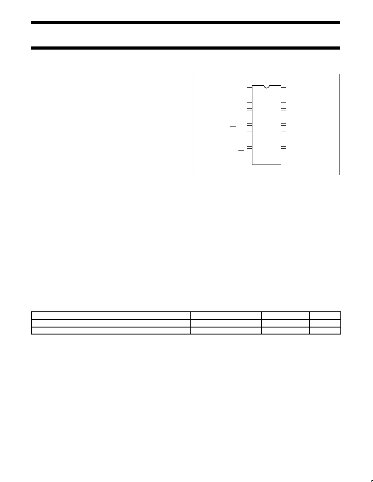
PIN CONFIGURATION
V
REF
(–)
1
2
3
4
5
6
7
8
9
10
11
12
13
14
20
19
18
17
16
15
V
IN
DB0
DB1
DB2
DB3
WR
/RDY
MODE
RD
INT
GND
V
DD
NC
OFL
DB7
DB6
DB5
DB4
CS
V
REF
(+)
TOP VIEW
D, F, N Packages
APPLICATIONS
•Microprocessor-based monitoring and control systems
•Transducer/µP interface
•Process control
•Logic analyzers
•Test and measurement
ORDERING INFORMATION
DESCRIPTION TEMPERATURE RANGE ORDER CODE DWG #
20-Pin Plastic Dual In-Line Package (DIP) 0 to +70°C ADC0820CNEN 0408B
20-Pin Plastic Small Outline (SO) package 0 to +70°C ADC0820CNED 1021B
Philips Semiconductors Linear Products Product specification
ADC0820
8-Bit, high-speed, µP-compatible A/D converter with
track/hold function
August 31, 1994
569
BLOCK DIAGRAM
∑
V
IN
V
REF
(+)
V
REF
(–)
V
REF
(+)
+
–
V
REF
(–)
V
REF
(–)
V
REF
16
(+)
OFL
4–BIT
FLASG
ADC
(4MSBs)
4–BIT
DAC
4–BIT
FLASG
ADC
(4LSBs)
MODE WR
/RDY
TIMING AND CONTROL CIRCUITRY
CS RD
INT
OUTPUT
LATCH
AND
THREE–STATE
BUFFERS
OFL
DB7
DB6
DB5
DB4
DB3
DB2
DB1
DB0
PIN DESCRIPTION
PIN NO SYMBOL DESCRIPTION
1 V
IN
Analog input; range=GND≤VIN≤V
DD
2 DB0 3-state data output—Bit 0 (LSB)
3 DB1 3-state data output—Bit 1
4 DB2 3-state data output—Bit 2
5 DB3 3-state data output—Bit 3
6 WR/RDY
WR-RD Mode
WR: With CS Low, the conversion is started on the falling edge of WR. Approximately 800ns (the preset internal time
out, t
I
) after the WR rising edge, the result of the conversion will be strobed into the output latch, provided that RD
does not occur prior to this time out (see Figures 3a and 3b).
RD Mode
RDY: This is an open-drain output (no internal pull-up device). RDY will go Low after the falling edge of CS; RDY will
go 3-State when the result of the conversion is strobed into the output latch. It is used to simplify the interface to a
microprocessor system (see Figure 1).
7 Mode Mode: Mode selection input—it is internally tied to GND through a 30µA current source.
RD Mode: When mode is Low.
WR-RD Mode: When mode is High.
8 RD
WR-RD Mode
With CS Low, the 3-State data outputs (DB0-DB7) will be activated when RD goes Low. RD can also be used to
increase the speed of the converter by reading data prior to the preset internal time out (T
I
~ 800ns). If this is done,
the data result transferred to output latch is latched after the falling edge of the RD
(see Figures 3a and 3b).
RD Mode
With CS Low, the conversion will start with RD going Low; also, RD will enable the 3-State data outputs at the
completion of the conversion. RDY going 3-State and INT
going Low indicate the completion of the conversion (see
Figure 1).
9 INT
WR-RD Mode
INT going Low indicates that the conversion is completed and the data result is in the output latch. INT will go
Low ~ 800ns (the preset internal time out, t
I
) after the rising edge of WR (see Figure 3a); or INT will go Low after
the falling edge of RD
, if RD goes Low prior to the 800ns time out (see Figure 3b). INT is reset by the rising edge of
RD
or CS (see Figures 3a and 3b).
Philips Semiconductors Linear Products Product specification
ADC0820
8-Bit, high-speed, µP-compatible A/D converter with
track/hold function
August 31, 1994
570
PIN DESCRIPTION (Continued)
PIN NO
SYMBOL DESCRIPTION
RD Mode
INT going Low indicates that the conversion is completed and the data result is in the output latch. INT is reset by
the rising edge of RD
or CS (see Figure 1).
10 GND Ground
11 V
REF
(-) The bottom of resistor ladder, voltage range: GND≤V
REF
(-)≤V
REF
(+)
12 V
REF
(+) The top of resistor ladder, voltage range: V
REF
(-)≤V
REF
(+)≤VDD.
13 CS CS must be Low in order for the RD or WR to be recognized by the converter.
14 DB4 3-State data output—Bit 4
15 DB5 3-State data output—Bit 5
16 DB6 3-State data output—Bit 6
17 DB7 3-State data output—Bit 7 (MSB)
18 OFL Overflow output—if the analog input is higher than the V
REF
(+)- LSB, OFL will be low at the end of conversion. It can
be used to cascade 2 or more devices to have more resolution (9, 10-bit). It is always active and never becomes
3-state.
19 NC No connection
20 V
DD
Power supply voltage
ABSOLUTE MAXIMUM RATINGS
1, 2
SYMBOL
PARAMETER RATING UNIT
V
DD
Supply voltage 7 V
Logic control inputs -0.2 to VDD+0.2 V
Voltage at other inputs and output -0.2 to VDD+0.2 V
T
STG
Storage temperature range -65 to +150 °C
P
D
Maximum power dissipation
3
TA=25°C(still-air)
N package 1690 mW
D package 1390 mW
T
SOLD
Lead temperature (soldering, 10sec) 300 °C
T
A
Operating ambient temperature range T
MIN≤TA≤TMAX
ADC0820CNEN/CNED 0 to +70 °C
NOTES:
1. Absolute Maximum Ratings are those values beyond which the life of the device may be impaired.
2. All voltages are measured with respect to GND, unless otherwise specified.
3. Derate above 25°C at the following rates:
N package at 13.5mW/°C
D package at 11.1mW/°C
Philips Semiconductors Linear Products Product specification
ADC0820
8-Bit, high-speed, µP-compatible A/D converter with
track/hold function
August 31, 1994
571
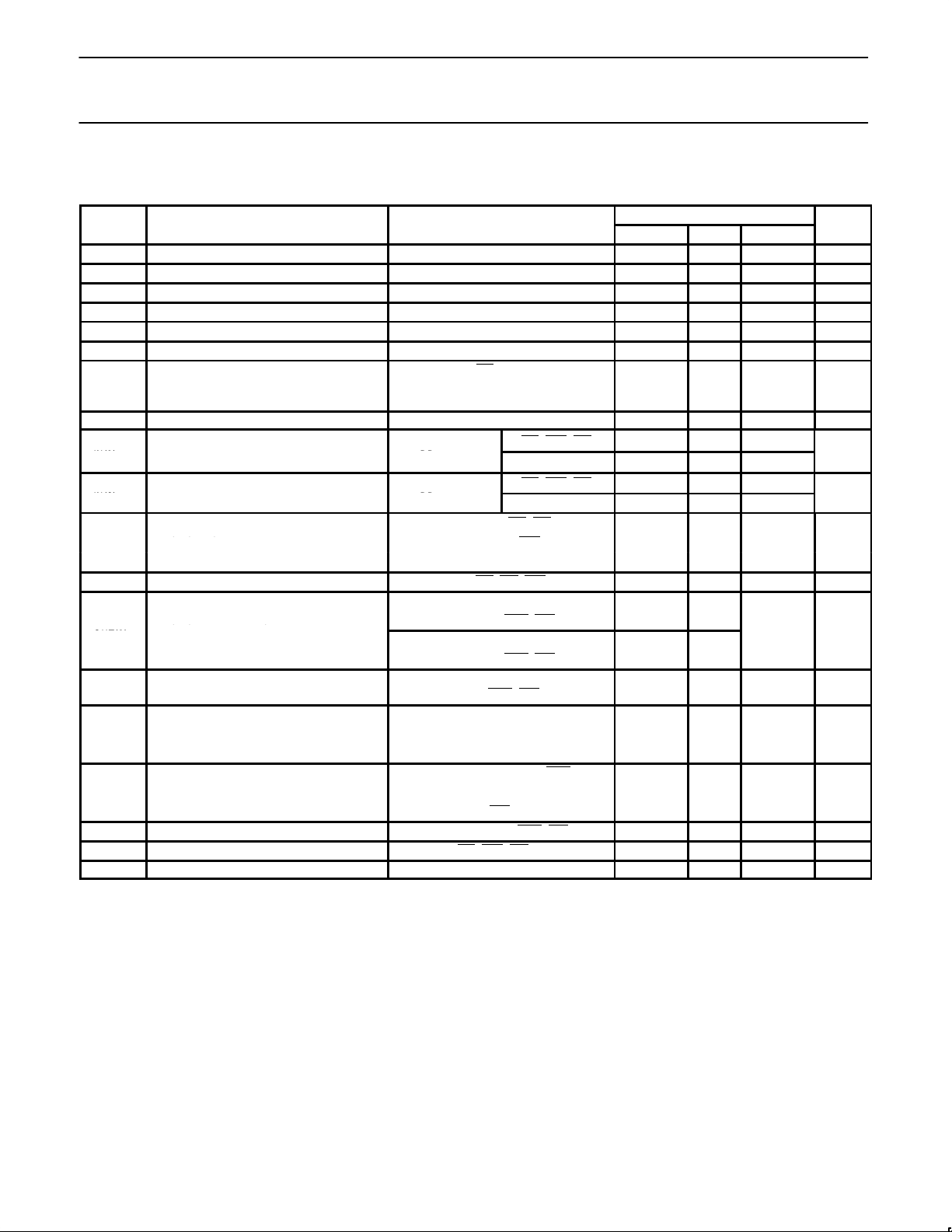
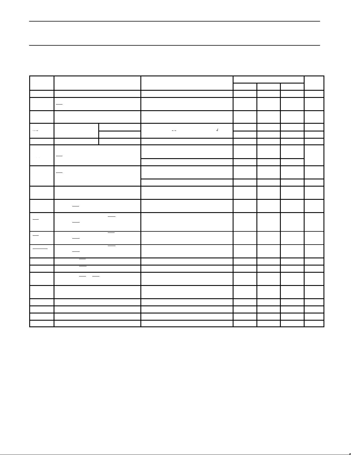
DC ELECTRICAL CHARACTERISTICS
RD mode (Pin 7=0), VDD=5V, V
REF
(+)=5V, and V
REF
(-)=GND, unless otherwise specified. Limits apply from T
MIN
to T
MAX
.
LIMITS
SYMBOL
PARAMETER
TEST CONDITIONS
Min Typ
3
Max
UNIT
Resolution 8 8 8 bits
Unadjusted error
1
ADC0820C ±1 LSB
R
REF
Reference resistance 1 1.6 4 kΩ
V
REF
(+) Input voltage
5
V
REF
(-) V
DD
V
V
REF
(-) Input voltage GND V
REF
(+) V
V
IN
Input voltage
5
GND-0.1 VDD+0.1 V
Maximum analog input leakage current
CS=V
DD
VIN=V
DD
VIN=GND
-3 3 µA
Power supply sensitivity VDD=5V±5% ±1/16 ±1/4 LSB
CS, WR, RD 2.0 V
DD
V
IN(1)
Logical “1” input voltage
VDD=5.25V
Mode 3.5 V
DD
V
CS, WR, RD GND 0.8
V
IN(0)
Logical “0” input voltage
VDD=4.75V
Mode GND 1.5
V
V
IN(1)
=5V; CS, RD 1
V
IN(1)
=5V; WR 3
µA
IN(1)
V
IN(1)
=5V; Mode 30 200
I
IN(0)
Logical “0” input current V
IN(0)
=0V; CS, RD, WR, Mode -1 µA
VDD=4.75V, I
OUT
=-360µA; 2.4 4.6
DB0-DB7, OFL, INT
V
OUT(1)
Logical “1” output voltage
VDD=4.75V, I
OUT
=-10µA 4.5 4.74
V
DB0-DB7, OFL, INT
V
OUT(0)
Logical “0” output voltage
VDD=4.75V, I
OUT
=1.6mA;
DB0-DB7, OFL
, INT, RDY
0.2 0.4 V
V
OUT
=5V; DB0-DB7, RDY 3
µA
OZ
V
OUT
=0V; DB0-DB7, RDY -3
V
OUT
=0V, DB0-DB7, OFL 6 12
SOURCE
INT 4.5 8
I
SINK
Output sink current V
OUT
=5V; DB0-DB7, OFL, INT, RDY 7 20 mA
I
DD
Supply current CS=WR=RD=0 6 15 mA
V
DD
Range 4.5 5.5 V
I
IN(1)
I
OZ
I
SOURCE
Logical “1” input current
3-state output current
Output source current mA
Philips Semiconductors Linear Products Product specification
ADC0820
8-Bit, high-speed, µP-compatible A/D converter with
track/hold function
August 31, 1994
572
AC ELECTRICAL CHARACTERISTICS
V
DD
= 5V, t
R
= t
F
= 20ns, V
REF(+)
= 5V, V
REF(-)
= 0V, and T
A
= 25°C, unless otherwise specified.
LIMITS
4
SYMBOL
PARAMETER
TEST CONDITIONS
Min Typ
3
Max
UNIT
t
CRD
Conversion time for RD mode Mode=0, Figure 1 1.6 2.5 µs
t
ACCO
Access time (delay from falling edge of
RD
to output valid)
Mode=0, Figure 1 t
CRD
+20 t
CRD
+50 ns
t
CWR-RD
Conversion time for WR-RD mode
Mode=VDD, tWR=600ns, tRD=600ns;
Figures 3a and 3b
1.52 µs
Min
600 ns
tWRWrite time
Max
Mode=VDD, Figures 3a and 3b
2
50 µs
t
RD
Read time Min Mode=VDD, Figures 3a and 3b
2
600 ns
Mode=VDD, tRD<tI;
Figure 3b, C
L
=15pF
190 280
t
ACC1
RD t o output valid)
CL=100pF 210 320
ns
t
ACC2
Access time (delay from falling edge of
RD
t o output valid)
Mode=VDD, tRD>tI;
Figure 3a, C
L
=15pF
70 120 ns
CL=100pF 90 150 ns
t
I
Internal comparison time
Mode=VDD;
Figures 2 and 3a, C
L
=50pF
800 1300 ns
t1H, t
0H
Three-state control (delay from rising
edge of RD
to Hi-Z state)
RL=1kΩ, CL=10pF 100 200 ns
t
INTL
Delay from rising edge of WR to falling
edge of INT
Mode=VDD, CL=50pF
t
RD>tI
; Figure 3a
t
RD<tI
; Figure 3b
t
RD
+200
t
I
tRD+290
ns
ns
t
INTH
Delay from rising edge of RD to rising
edge of INT
Figures 1, 3a, and 3b,
C
L
=50pF
125 225 ns
t
INTHWR
Delay from rising edge of WR to rising
edge of INT
Figure 2, CL=50pF 175 270 ns
t
RDY
Delay from CS to RDY Figure 1, CL=50pF, Mode=0 50 100 ns
t
ID
Delay from INT to output valid Figure 2 20 50 ns
t
RI
Delay from RD to INT
Mode=VDD, tRD<tI;
Figure 3b
200 290 ns
t
P
Delay from end of conversion to next
conversion
Figures 1, 2, 3a, and 3b
2
500 ns
SR Slew rate, tracking 0.1 V/µs
C
VIN
Analog input capacitance 45 pF
C
OUT
Logic output capacitance 5 pF
C
IN
Logic input capacitance 5 pF
NOTES:
1. Unadjusted error includes offset, full-scale, and linearity errors.
2. Accuracy may degrade if t
WR
or tRD is shorter than the minimum value specified.
3. Typical values are at 25°C and represent most likely parametric norm.
4. Guaranteed but not 100% production tested. These limits are not used to calculate outgoing quality levels.
5. V
REF
and VIN must be applied after VCC has been turned on to prevent possibility of latching.
t
ACC1
Access time (delay from falling edge of
ns