Philips adc0803x DATASHEETS

Philips Semiconductors Linear Products Product specification
ADC0803/4-1CMOS 8-bit A/D converters
555
August 31, 1994 853-0034 13721
DESCRIPTION
The ADC0803 family is a series of three CMOS 8-bit successive
approximation A/D converters using a resistive ladder and
capacitive array together with an auto-zero comparator. These
converters are designed to operate with microprocessor-controlled
buses using a minimum of external circuitry. The 3-State output data
lines can be connected directly to the data bus.
The differential analog voltage input allows for increased
common-mode rejection and provides a means to adjust the
zero-scale offset. Additionally, the voltage reference input provides a
means of encoding small analog voltages to the full 8 bits of
resolution.
FEATURES
•Compatible with most microprocessors
•Differential inputs
•3-State outputs
•Logic levels TTL and MOS compatible
•Can be used with internal or external clock
•Analog input range 0V to V
CC
•Single 5V supply
•Guaranteed specification with 1MHz clock
PIN CONFIGURATION
1
2
3
4
5
6
7
8
9
10
11
12
13
14
20
19
18
17
16
15
D
1
,
N PACKAGES
CS
RD
WR
INTR
CLK IN
V
IN
(+)
V
IN
(–)
A GND
V
REF
/2
D GND
V
CC
CLK R
D0
D1
D2
D3
D4
D5
D6
D7
TOP VIEW
NOTE:
SOL — Released in large SO package only.
TEMPERATURE RANGE ORDER CODE DWG #
20-Pin Plastic Dual In-Line Package (DIP) -40 to +85°C ADC0803/04-1 LCN 0408B
20-Pin Plastic Dual In-Line Package (DIP) 0 to 70°C ADC0803/04-1 CN 0408B
20-Pin Plastic Small Outline (SO) Package 0 to 70°C ADC0803/04-1 CD 1021B
20-Pin Plastic Small Outline (SO) Package -40 to 85°C ADC0803/04-1 LCD 1021B
ABSOLUTE MAXIMUM RATINGS
SYMBOL PARAMETER RATING UNIT
V
CC
Supply voltage 6.5 V
Logic control input voltages -0.3 to +16 V
All other input voltages
-0.3 to
(V
CC
+0.3)
V
T
A
Operating temperature range
ADC0803/04-1 LCD -40 to +85 °C
ADC0803/04-1 LCN -40 to +85 °C
ADC0803/04-1 CD 0 to +70 °C
ADC0803/04-1 CN 0 to +70 °C
T
STG
Storage temperature -65 to +150 °C
T
SOLD
Lead soldering temperature (10 seconds) 300 °C
P
D
Maximum power dissipation
T
A
=25°C (still air)
1
N package 1690 mW
D package 1390 mW
NOTES:
1. Derate above 25°C, at the following rates: N package at 13.5mW/°C; D package at 11.1mW/°C
APPLICATIONS
•Transducer-to-microprocessor interface
•Digital thermometer
•Digitally-controlled thermostat
•Microprocessor-based monitoring and control systems
ORDERING INFORMATION
DESCRIPTION

Philips Semiconductors Linear Products Product specification
ADC0803/4-1CMOS 8-bit A/D converters
August 31, 1994
556
BLOCK DIAGRAM
M
VIN (+) VIN (–)
76
+
–
LADDER AND
DECODER
+
–
AUTO ZERO
COMPARATOR
V
REF
/2
A GND
9
8
V
CC
20
10
D GND
WR
CS
RD
3
1
2
SAR
8–BIT
SHIFT REGISTER
INTR
FF
CLOCK
OUTPUT
LATCHES
LE OE
D7 (MSB) (11)
D6 (12)
D5 (13)
D4 (14)
D3 (15)
D2 (16)
D1 (17)
D0 (LSB) (18)
INTR
CLK IN
CLK R
S
R Q
5 4 19

Philips Semiconductors Linear Products Product specification
ADC0803/4-1CMOS 8-bit A/D converters
August 31, 1994
557
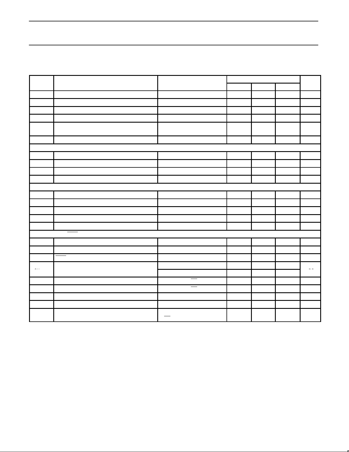
DC ELECTRICAL CHARACTERISTICS
V
CC
= 5.0V, f
CLK
= 1MHz, T
MIN
≤ TA ≤ T
MAX
, unless otherwise specified.
ADC0803/4
SYMBOL
PARAMETER
TEST CONDITIONS
Min Typ Max
UNIT
ADC0803 relative accuracy error (adjusted) Full-Scale adjusted 0.50 LSB
ADC0804 relative accuracy error (unadjusted) V
REF
/2 = 2.500V
DC
1 LSB
R
IN
V
REF
/2 input resistance
3
VCC = 0V
2
400 680 Ω
Analog input voltage range
3
–0.05 VCC+0.05 V
DC common-mode error
Over analog input voltage
range
1/16 1/8 LSB
Power supply sensitivity VCC = 5V ±10%
1
1/16 LSB
Control inputs
V
IH
Logical “1” input voltage VCC = 5.25V
DC
2.0 15 V
DC
V
IL
Logical “0” input voltage VCC = 4.75V
DC
0.8 V
DC
I
IH
Logical “1” input current VIN = 5V
DC
0.005 1 µA
DC
I
IL
Logical “0” input current VIN = 0V
DC
–1 –0.005 µA
DC
Clock in and clock R
VT+ Clock in positive-going threshold voltage 2.7 3.1 3.5 V
DC
VT– Clock in negative-going threshold voltage 1.5 1.8 2.1 V
DC
V
H
Clock in hysteresis (VT+)–(VT–) 0.6 1.3 2.0 V
DC
V
OL
Logical “0” clock R output voltage IOL = 360µA, VCC = 4.75V
DC
0.4 V
DC
V
OH
Logical “1” clock R output voltage IOH = –360µA, VCC = 4.75V
DC
2.4 V
DC
Data output and INTR
V
OL
Logical “0” output voltage
Data outputs IOL = 1.6mA, VCC = 4.75V
DC
0.4 V
DC
INTR outputs IOL = 1.0mA, VCC = 4.75V
DC
0.4 V
DC
IOH = –360µA, VCC = 4.75V
DC
2.4
VOHLogical “1” output voltage
IOH = –10µA, VCC = 4.75V
DC
4.5
V
DC
I
OZL
3-state output leakage V
OUT
= 0VDC, CS = logical “1” –3 µA
DC
I
OZH
3-state output leakage V
OUT
= 5VDC, CS = logical “1” 3 µA
DC
I
SC
+Output short-circuit current V
OUT
= 0V, TA = 25°C 4.5 12 mA
DC
I
SC
–Output short-circuit current V
OUT
= VCC, TA = 25°C 9.0 30 mA
DC
I
CC
Power supply current
f
CLK
= 1MHz, V
REF
/2 = OPEN,
CS
= Logical “1”, TA = 25°C
3.0 3.5 mA
NOTES:
1. Analog inputs must remain within the range: –0.05 ≤ VIN ≤ VCC + 0.05V.
2. See typical performance characteristics for input resistance at VCC = 5V.
3. V
REF
/2 and VIN must be applied after the VCC has been turned on to prevent the possibility of latching.

Philips Semiconductors Linear Products Product specification
ADC0803/4-1CMOS 8-bit A/D converters
August 31, 1994
558
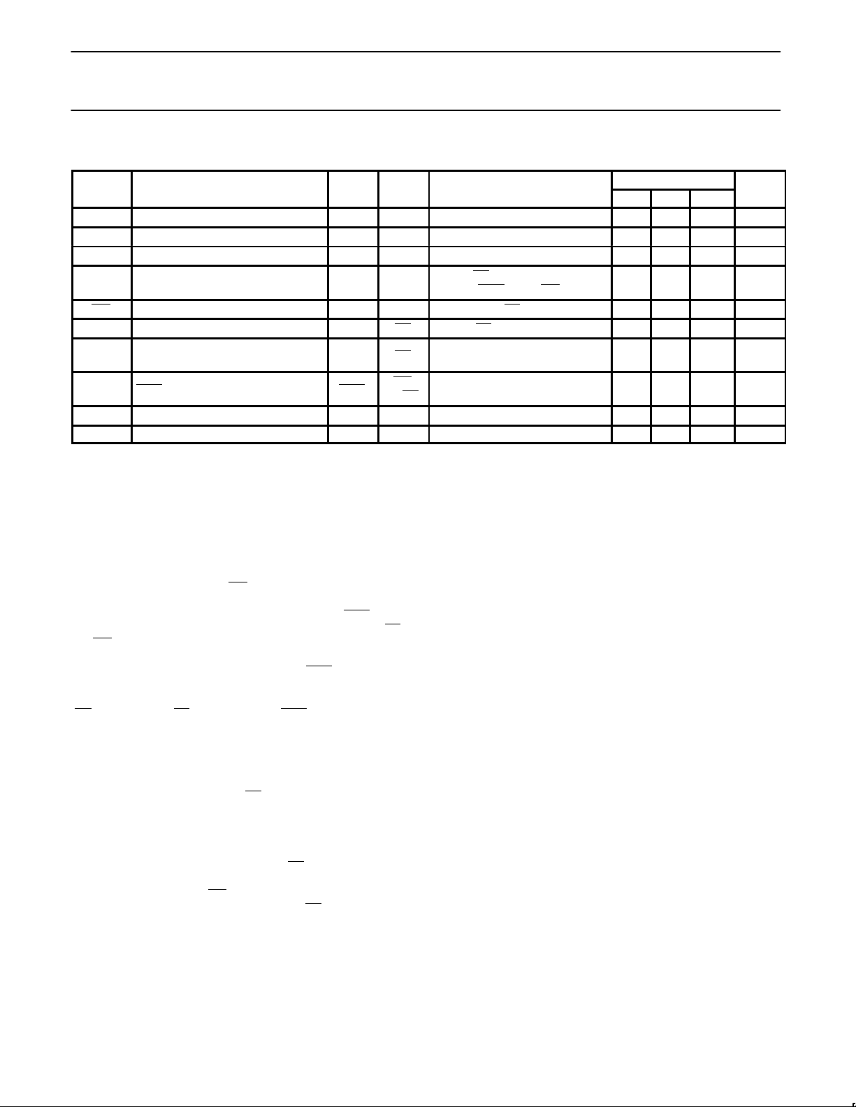
AC ELECTRICAL CHARACTERISTICS
ADC0803/4
SYMBOL
PARAMETER
TO
FROM
TEST CONDITIONS
Min Typ Max
UNIT
Conversion time f
CLK
=1MHz
1
66 73 µs
f
CLK
Clock frequency
1
0.1 1.0 3.0 MHz
Clock duty cycle
1
40 60 %
CR Free-running conversion rate
CS=0, f
CLK
=1MHz
INTR
tied to WR
13690 conv/s
tW(WR)L Start pulse width CS=0 30 ns
t
ACC
Access time Output RD CS=0, CL=100pF 75 100 ns
t1H, t
0H
3-State control Output RD
CL=10pF, RL=10kΩ
See 3-State test circuit
70 100 ns
tW1, t
R1
INTR delay INTR
WD
or RD
100 150 ns
C
IN
Logic input=capacitance 5 7.5 pF
C
OUT
3-State output capacitance 5 7.5 pF
NOTES:
1. Accuracy is guaranteed at f
CLK
=1MHz. Accuracy may degrade at higher clock frequencies.
FUNCTIONAL DESCRIPTION
These devices operate on the Successive Approximation principle.
Analog switches are closed sequentially by successive
approximation logic until the input to the auto-zero comparator
[ V
IN
(+)-VIN(-) ] matches the voltage from the decoder. After all bits
are tested and determined, the 8-bit binary code corresponding to
the input voltage is transferred to an output latch. Conversion begins
with the arrival of a pulse at the WR
input if the CS input is low. On
the High-to-Low transition of the signal at the WR or the CS input,
the SAR is initialized, the shift register is reset, and the INTR
output
is set high. The A/D will remain in the reset state as long as the CS
and WR inputs remain low. Conversion will start from one to eight
clock periods after one or both of these inputs makes a Low-to-High
transition. After the conversion is complete, the INTR
pin will make a
High-to-Low transition. This can be used to interrupt a processor, or
otherwise signal the availability of a new conversion result. A read
(RD
) operation (with CS low) will clear the INTR line and enable the
output latches. The device may be run in the free-running mode as
described later. A conversion in progress can be interrupted by
issuing another start command.
Digital Control Inputs
The digital control inputs (CS, WR, RD) are compatible with
standard TTL logic voltage levels. The required signals at these
inputs correspond to Chip Select, START Conversion, and Output
Enable control signals, respectively. They are active-Low for easy
interface to microprocessor and microcontroller control buses. For
applications not using microprocessors, the CS
input (Pin 1) can be
grounded and the A/D START function is achieved by a
negative-going pulse to the WR
input (Pin 3). The Output Enable
function is achieved by a logic low signal at the RD
input (Pin 2),
which may be grounded to constantly have the latest conversion
present at the output.
ANALOG OPERATION
Analog Input Current
The analog comparisons are performed by a capacitive charge
summing circuit. The input capacitor is switched between V
IN(+)
4
and V
IN(-)
, while reference capacitors are switched between taps on
the reference voltage divider string. The net charge corresponds to
the weighted difference between the input and the most recent total
value set by the successive approximation register.
The internal switching action causes displacement currents to flow
at the analog inputs. The voltage on the on-chip capacitance is
switched through the analog differential input voltage, resulting in
proportional currents entering the V
IN(+)
input and leaving the V
IN(-)
input. These transient currents occur at the leading edge of the
internal clock pulses. They decay rapidly so do not inherently cause
errors as the on-chip comparator is strobed at the end of the clock
period.
Input Bypass Capacitors and Source Resistance
Bypass capacitors at the input will average the charges mentioned
above, causing a DC and an AC current to flow through the output
resistance of the analog signal sources. This charge pumping action
is worse for continuous conversions with the V
IN(+)
input at full
scale. This current can be a few microamps, so bypass capacitors
should NOT be used at the analog inputs of the V
REF
/2 input for
high resistance sources (> 1kΩ). If input bypass capacitors are
desired for noise filtering and a high source resistance is desired to
minimize capacitor size, detrimental effects of the voltage drop
across the input resistance can be eliminated by adjusting the full
scale with both the input resistance and the input bypass capacitor
in place. This is possible because the magnitude of the input current
is a precise linear function of the differential voltage.
 Loading...