

Page 1
1PHILIPS AA5 (AB) Chassis
Recommended Safety Parts
Item Part No. Description
4822 256 92053 Fuse holder
4822 276 12597 Mains switch
4822 492 70158 Spring for TS7540-7400
4822 265 30389 2 pins male for degaussing
4822 265 40596 2 pins male for mains
4822 267 60243 21 pins euroconnector
1001 4822 210 10448 UV915E/IEC
1001 4822 210 10459 UV913/IEC
1001 4822 210 10464 U943C/IEC
1001 4822 210 10554 UV917/IEC
1449 4822 071 54001 Fuse 400 mA
1500 4822 070 33152 Fuse 3.15A
1501 4822 070 33152 2183.15 (3.15A)
1540 4822 071 58001 Fuse 800 mA
1571 4822 071 56301 Fuse 630 mA
1572 4822 252 51173 Fuse 1.000 mA
1710 4822 071 51601 Fuse 160 mA
2015 4822 124 41525 100uF 20% 25V
2017 4822 124 41579 10uF 20% 50V
2041 5322 126 10223 4.7nF 10% 63V
2043 5322 126 10223 4.7nF 10% 63V
2044 5322 126 10223 4.7nF 10% 63V
2080 5322 122 32654 22nF 10% 63V
2101 5322 126 10223 4.7nF 10% 63V
2117 5322 126 10223 4.7nF 10% 63V
2124 4822 124 41579 10pF 20% 50V
2125 5322 122 32654 22nF 10% 63V
2129 4822 124 41579 10pF 20% 50V
2151 4822 122 33177 10nF 20% 50V
2157 4822 124 41525 100uF 20% 25V
2157 5322 122 34123 1nF 10% 50V
2158 5322 126 10223 4.7nF 10% 63V
2170 4822 122 33177 10nF 20% 50V
2171 5322 126 10223 4.7nF 10% 63V
2180 4822 124 41579 10uF 20% 50V
2248 4822 124 41579 10uF 20% 50V
2261 4822 122 33177 10nF 20% 50V
2263 5322 122 32654 22nF 10% 63V
2264 4822 122 33177 10nF 20% 50V
2271 5322 122 32654 22nF 10% 63V
2272 5322 122 34123 1nF 10% 50V
2273 5322 122 34123 1nF 10% 50V
2291 4822 122 33177 10nF 20% 50V
2292 4822 122 33177 10nF 20% 50V
2293 4822 122 33177 10nF 20% 50V
2350 5322 126 10223 4.7nF 10% 63V
2354 4822 122 33177 10nF 20% 50V
2366 5322 126 10223 47nF 10% 63V
2371 5322 122 32654 22nF 10% 63V
2401 4822 122 33172 390pF 5% 50V
2414 5322 126 10223 4.7nF 10% 63V
2445 4822 126 11503 820pF 10% 2KV
2445 4822 126 13435 1.2nF 10% 2KV
2446 4822 121 70618 12nF 5% 1600V
2446 4822 121 70637 8.2nF 5% 1600V
2448 4822 124 80096 47uF 200V
2450 5322 121 44128 680nF 10% 250V
2456 5322 122 34123 1nF 10% 50V
2482 5322 122 32654 22nF 10% 63V
2500 4822 126 13589 470nF 275V
2502 4822 126 11141 2.2nF 10%1KV
2504 4822 126 11141 2.2nF 10%1KV
2505 4822 124 42104 68uF 20% 385V
2506 4822 126 10727 3.3nF 20% 400V
2506 4822 126 11141 2.2nF 10% 1KV
2511 4822 126 11141 2.2nF 10% 1KV
2512 4822 126 11141 2.2nF 10% 1KV
2524 4822 126 11382 1nF 10% 1KV
2525 4822 124 41525 100uF 20% 25V
2530 4822 124 80096 47uF 200V
2534 4822 126 11524 1.5nF 10%1KV
2540 4822 126 13337 220pF 10% 1KV
2550 4822 126 10727 3.3nF 20% 400V
2552 4822 126 11382 1nF 10%1KV
2568 4822 126 12274 1500pF 10% R(HR) 2KV
2569 4822 124 80096 47uF 200V
2602 4822 124 41579 10uF 20% 50V
2630 4822 124 41579 10uF 20% 50V
2660 5322 122 34123 1nF 10% 50V
2662 5322 126 10223 4.7nF 10% 63V
Recommended Safety Parts
Item Part No. Description
2663 5322 126 10223 4.7nF 10% 63V
2685 4822 124 41525 100uF 20% 25V
2686 5322 122 32654 22nF 10% 63V
2689 4822 122 33177 10nF 20% 50V
2734 4822 124 41579 10uF 20% 50V
2752 4822 124 40433 47uF 20% 25V
2848 4822 124 41579 10uF 20% 50V
2860 5322 126 10223 4.7nF 10% 63V
3001 4822 052 10129 12Ω 5% 0.33W
3001 4822 052 10279 27Ω 5% 0.33W
3007 4822 116 83953 75Ω 5% 0.125W
3019 4822 051 20008 0Ω jumper SMD
3032 4822 051 20121 120Ω 5% 0.1W
3124 4822 052 10109 10Ω 5% 0.33W
3141 4822 051 10472 4k7 2% 0.25W
3160 4822 117 11649 82Ω 5%
3161 4822 117 11649 82Ω 5%
3257 4822 116 83953 75Ω 5% 0.125W
3292 4822 051 10103 10k 2% 0.25W
3295 4822 051 10103 10k 2% 0.25W
3306 4822 051 20008 0Ω jumper SMD
3345 4822 052 10109 10Ω 5% 0.33W
3345 4822 052 11471 470Ω 5% 0.5W
3401 4822 052 10222 2k2 5% 0.33W
3404 4822 051 20472 4k7 5% 0.1W
3408 4822 052 10222 2k2 5% 0.33W
3408 4822 053 10681 680Ω 5% 1W
3409 4822 051 10103 10k 2% 0.25W
3411 4822 052 10228 2Ω2 5% 0.33W
3411 4822 052 10278 2Ω7 5% 0.33W
3412 4822 052 10228 2Ω2 5% 0.33W
3412 4822 052 10278 2Ω7 5% 0.33W
3415 4822 050 21802 1k8 1% 0.6W
3416 4822 050 21802 1k8 1% 0.6W
3421 4822 053 12279 27Ω 5% 3W
3448 4822 052 10108 1Ω 5% 0.33W
3448 4822 052 10228 2Ω2 5% 0.33W
3449 4822 052 10108 1Ω 5% 0.33W
3452 4822 052 10108 1Ω 5% 0.33W
3452 4822 052 11338 3Ω3 5% 0.5W
3454 4822 052 11102 1k 5% 0.5W
3469 4822 052 10478 4Ω7 5% 0.33W
3470 4822 052 10828 8Ω2 5% 0.33W
3501 4822 116 40137 PTC 36Ω 365V
3503 4822 053 21475 4M7 5% 0.5W
3504 4822 053 21475 4M7 5% 0.5W
3506 4822 116 40137 PTC 36Ω 365V
3523 4822 050 24708 4Ω7 1% 0.6W
3524 4822 052 10229 22Ω 5% 0.33W
3528 4822 050 24708 4Ω7 1% 0.6W
3529 4822 053 11689 68Ω 5% 2W
3533 4822 050 24703 47k 1% 0.6W
3544 4822 052 10108 1Ω5% 0.33W
3547 4822 050 21802 1k8 1% 0.6W
3549 4822 053 21475 4M7 5% 0.5W
3550 4822 053 21475 4M7 5% 0.5W
3554 4822 053 11689 68Ω 5% 2W
3557 4822 053 11271 270Ω 5% 2W
3564 4822 050 21202 1k2 1% 0.6W
3573 4822 053 11102 1k 5% 2W
3608 4822 051 20472 4k7 5% 0.1W
3617 4822 051 20472 4k7 5% 0.1W
3623 4822 051 10103 10k 2% 0.25W
3671 4822 051 10103 10k 2% 0.25W
3695 4822 051 20472 4k7 5% 0.1W
3696 4822 051 20472 4k7 5% 0.1W
3697 4822 051 20472 4k7 5% 0.1W
3701 4822 052 10108 10 5% 0.33W
3707 4822 051 20472 4k7 5% 0.1W
3722 4822 051 20472 4k7 5% 0.1W
3749 4822 053 10159 15Ω 5% 1W
3760 4822 051 20472 4k7 5% 0.1W
3761 4822 051 20472 4k7 5% 0.1W
3851 4822 116 83953 75Ω 5% 0.125W
3853 4822 116 83953 75Ω 5% 0.125W
3855 4822 116 83953 75Ω 5% 0.125W
3858 4822 116 83953 75Ω 5% 0.125W
3875 4822 116 83953 75Ω 5% 0.125W
5445 4822 140 10406 LOT AT2079/40
5453 4822 157 51462 10uH 10%
Recommended Safety Parts
Item Part No. Description
5500 4822 157 53348 Mains filter (2x)
5500 4822 212 22978 Mains filter (1x)
5501 4822 157 53348 Mains filter (2x)
5515 4822 157 50963 2.2uH 20%
5560 4822 157 51462 10uH 10%
5601 4822 157 51462 10uH 10%
6053 4822 130 30621 1N4148
6113 4822 130 30621 1N4148
6141 4822 130 30621 1N4148
6481 4822 130 34499 BZX79-C20
6502 4822 130 31933 1N5061
6503 4822 130 31933 1N5061
6504 4822 130 31933 1N5061
6505 4822 130 31933 1N5061
6510 4822 130 31933 1N5061
6511 4822 130 31933 1N5061
6512 4822 130 31933 1N5061
6513 4822 130 31933 1N5061
6522 4822 130 30621 1N4148
6524 4822 130 31631 BYV10-20
6530 4822 130 30621 1N4148
6568 4822 130 81175 BYD74G
6658 4822 130 30621 1N4148
6663 4822 209 30563 TLXR5400
6849 4822 130 30621 1N4148
7030 5322 130 41982 BC848B
7126 5322 130 41982 BC848B
7127 5322 130 41982 BC848B
7141 5322 130 41982 BC848B
7142 5322 130 41982 BC848B
7143 5322 130 41982 BC848B
7170 5322 130 41982 BC848B
7242 5322 130 41982 BC848B
7243 5322 130 41982 BC848B
7408 5322 130 41982 BC848B
7514 4822 130 91451 CQY80NG
7540 4822 130 63409 STP6N60FI
7567 4822 209 80591 LM317T
7571 5322 130 41982 BC848B
7640 5322 130 41982 BC848B
7641 4822 130 44197 BC558B
7642 4822 130 41344 BC337-40
7654 5322 130 41982 BC848B
7657 5322 130 41982 BC848B
7665 5322 130 41982 BC848B
7670 5322 130 41982 BC848B
7672 5322 130 41982 BC848B
7674 5322 130 41982 BC848B
7686 5322 130 41982 BC848B
7710 5322 130 41982 BC848B
7711 5322 130 41982 BC848B
7713 5322 130 41982 BC848B
7715 5322 130 41982 BC848B
7732 5322 130 41982 BC848B
7751 4822 130 41344 BC337-40
7754 5322 130 41982 BC848B
7755 5322 130 41982 BC848B
7856 5322 130 41982 BC848B
7858 5322 130 41982 BC848B
7875 5322 130 41982 BC848B
7876 5322 130 41982 BC848B
4822 255 70306 Holder valve mini neck
2282 5322 122 32654 22nF 10% 63V
3235 4822 052 1018 1Ω 5% 0.33W
7206 5322 130 41982 BC848B
7219 5322 130 41982 BC848B
7228 5322 130 41982 BC848B
4822 255 70305 Holder valve narrow neck
2209 5322 122 32654 22nF 10% 63V
2214 4822 126 13451 2.2nF 10% 2KV
7235 5322 130 41982 BC848B
7240 4822 130 44197 BC558B
7245 5322 130 41982 BC848B
7255 5322 130 41982 BC848B
1236 4822 052 10108 1R00 5% 0,33W
1236 4822 071 51002 Fuse 1A T
1449 4822 071 54001 Fuse 400 mAT
2401 4822 122 33172 390pF 5% 50V
2401 5322 122 34123 1nF 10% 50V
2445 4822 126 11503 820pF 10% 2kV
Recommended Safety Parts
Item Part No. Description
2445 4822 126 12267 470pF 10%R (HR) 2kV
2445 4822 126 13435 1.2nF 10% 2kV
2445 4822 126 13449 1nF 10% 2kV
2445 4822 126 72274 1n5 10% 2kV
2446 4822 121 70618 12nF 5% 1600V
2446 4822 121 70637 8.2nF 5% 1600V
2446 4822 121 70649 9.1nF 5% 1.6kV
2450 4822 121 42365 330nF 5% 250V
2450 4822 121 42634 560nF 5% 250V
2450 4822 121 70711 0.47uF 5% 250V
2450 5322 121 44128 680nF 5% 250V
2456 5322 122 32531 100pF 5% 50V
2456 5322 122 34123 1nF 10% 50V
2505 4822 124 42104 68uF 20% 385V
2505 4822 157 71702 150uF 20% 385V
2540 4822 126 13337 220pF 10% 1kV
2568 4822 126 12267 470pF 10%R (HR) 2kV
2568 4822 126 12274 1500pF 10%R (HR) 2kV
2706 4822 124 41579 10uF 20% 50V
3001 4822 052 10629 56Ω 5% 0.33W
3001 4822 052 10399 39Ω 5% 0.33W
3001 4822 052 10229 22Ω 5% 0.33W
3267 4822 053 12123 12k 5% 3W
3267 4822 053 12153 15k 5% 3W
3277 4822 053 12123 12k 5% 3W
3277 4822 053 12153 12k 5% 3W
3287 4822 053 12123 12k 5% 3W
3287 4822 053 12153 15k 5% 3W
3401 4822 052 10222 2k2 5% 0.33W
3401 4822 052 10392 3k9 5% 0.33W
3401 4822 117 11824 2k2 5% 0.33W
3401 4822 052 11102 1k 5% 0.33W
3408 4822 052 10222 2k2 5% 0.33W
3408 4822 052 10392 3k9 5% 0.33W
3408 4822 052 11152 1k5 5% 0.5W
3408 4822 053 10681 680Ω 5% 1W
3408 4822 052 11102 1k 5% 0.5W
3411 4822 052 10158 1Ω5 5% 0.33W
3411 4822 052 10278 2Ω7 5% 0.33W
3411 4822 052 10338 3Ω3 5% 0.33W
3412 4822 052 10228 2Ω2 5% 0.33W
3412 4822 052 10278 2Ω7 5% 0.33W
3412 4822 052 10338 3Ω3 5% 0.33W
3412 4822 052 10158 1R5 5% 0.33W
3420 4822 053 11102 1k 5% 2W
3420 4822 053 11561 560Ω 5% 2W
3420 4822 117 10483 910Ω 5% 2W
3421 4822 053 12279 27Ω 5% 3W
3421 4822 053 12399 39Ω 5% 3W
3449 4822 052 10108 1Ω 5% 0.33W
3452 4822 052 10108 1Ω 5% 0.33W
3452 4822 052 10338 3Ω3 5% 0.33W
3452 4822 052 10478 4Ω7 5% 0.33W
3452 4822 052 10568 5Ω6 5% 0.33W
3452 4822 052 10828 8Ω2 5% 0.33W
3454 4822 052 11102 1k 5% 0.5W
3469 4822 052 10478 4Ω7 5% 0.33W
3470 4822 052 10478 4Ω7 5% 0.33W
3470 4822 052 10828 8Ω2 5% 0.33W
3506 4822 116 40137 FTC 36Ω 365V
3506 4822 116 40282 FTC 22Ω 276V
3749 4822 050 24708 4R7 1% 1/6W
3749 4822 050 26808 6Ω8 1% 0.6W
3749 4822 053 10159 15Ω 5% 1W
5445 4822 140 10406 LOT uS 4
5445 4822 140 10544 LOT uSLOT S
5445 4822 140 10543 LOT LOT110
2401 4822 121 40479 390nF 10% 250V
2404 4822 121 40488 22nF 10% 400V
2405 4822 121 40479 390nF 10% 250V
3402 4822 052 10561 560Ω 5% 0.33W
3404 4822 052 10479 47Ω 5% 0.33W
3422 4822 053 10681 680Ω 5% 1W
5401 4822 157 63079 COIL
5402 4822 157 53069 COIL
6401 4822 130 83342 BY228-RAP15/10
6402 4822 130 41602 BYW95C/20
6403 4822 130 30621 1N4148 (COL)
7402 4822 130 44197 BC558B
7403 4822 130 40981 BC337-25
Electrical
Adjustments
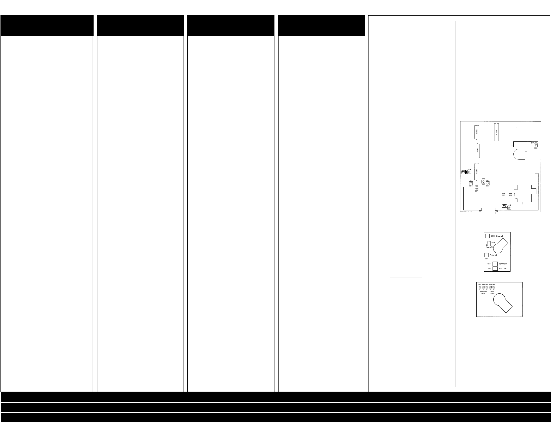
1. Adjustments on the main panel (Fig. 7.1)
1.1 +100V power supply voltage
Connect a voltmeter (DC) across 02530. Adjust
R3532 at a black picture (beam current 0 mA)
for a voltage of:
- +100V for l4-15-17”
- +92V5 for 20” narrow neck (neck diameter
approx 30 mm) and 21” mini neck (neck
diameter approx
20 mm) at a black picture
- +86V for 21’ narrow neck (neck diameter
approx 30 mm)
1.2 Horizontal centring
Is adjusted with potentiometer R3354.
1.3 Picture height
Is adjusted with potentiometer R3410.
1.4 Vertical centring
Can be adjusted by eventually mounting one of
the resistors R3401 and/or R3408.
1.5 Focusing
Is adjusted with the focusing potentiometer in
the line output transformer.
1.6 IF filter (only for sets with SECAM LL’
reception possibility):
Connect a signal generator (e.g. PM5326) via a
capacitor of 5p6 to pin 17 of the tuner and
adjust the frequency for 40.4 MHz.
Connect an oscilloscope to pin 1 of filter 1015.
Switch on the set and select system Europe
(BG/L is “low” for BGIDK reception).
Adjust L5012 for a minimum amplitude.
1.7 AFC
a. For sets with SECAM LL’ reception possibility:
Connect a signal generator (e.g. PM5326) as
indicated in point 1 .6. Connect a voltmeter to
pin 44 of IC7015/6A.
Adjust the frequency for 33.9 MHz and select
system France (L/L’ is “high” for L’ reception).
Adjust L5040 for 3V5 (DC).
Next adjust the frequency for 38.9 MHz and
select system Europe (L/L’ is “low” for
BGILDK reception). Adjust L5043 for 3V5
(DC).
b. For sets without SECAM LL’ reception
possibility:
Connect a signal generator (e.g. PM5326) as
indicated above and adjust the frequency for
38.9 MHz (for PAL I at 39.5 MHz). Connect a
voltmeter to pin 44 of IC7015/6A. Adjust
L5040 for 3V5 (DC).
1.8 RF AGC
If the picture of a strong local transmitter is
reproduced distorted, adjust potentiometer
R3021 until the picture is undistorted.
Or: Connect a pattern generator (e.g. PM5518)
to the aerial input with RF signal amplitude =1 mV .
Connect a multimeter (DC) at pin 5 of tuner.
Adjust R3021 so that voltage at pin 5 of tuner is
7V5 ± 0V5 (DC).
2. Adjustments on the CRT panel (Fig. 7.2)
2.1 Vg2 cut-off points of picture tube
Apply a pattern generator (e.g PM5518) and set
it to a white raster pattern. Adjust contrast and
Vg2 at minimum (Vg2 with potentiometer in line
output transformer to the left). Adjust brightness
until the DC voltage across potentiometer 3213
is 0V. Adjust R3207 (B), R3220 (G) and R3234
(R) for a level of 125V for 14-1 5-17-21” mini
neck (neck diameter of approx 20 mm) on the
collectors of transistors 7205, 7218 and 7227.
Adjust R3264 (B), R3274 (G) and R3302 (R) for
a level of 150V for 20” narrow neck and 160V
for 21” narrow neck (both neck diameter of
approx 30 mm) on the collectors of TS7265,
7275 and 7285. Adjust Vg2 potentiometer until
the light from the gun that first emits light is just
no longer visible. Adjust the two other guns with
the respective controls (3207, 3220 or 3234 or
for mini neck and 3264, 3274 or 3302 for narrow
neck) until just no light will be visible.
2.2 Grey scale (white D)
Apply a grey scale and adjust the set for normal
operation. Allow the set to warm up for about 10
minutes. Adjust R3213 and R3214 (R3263 and
R3273 for 20-21” narrow neck) until the desired
grey scale has been obtained.
Main carrier (component side)
Fig. 7.1
CRT panel mini neck 14-15-17-21”
CRT panel narrow neck 20”
Fig. 7.2
Repair facilities
Functional blocks
On both the service printing on the copper and
the component side, functional blocks are
indicated by a line and text.
Test points
The AA5 chassis is equipped with test points in
the service printing on both sides of monoboard. These test points are referring to the
functional blocks as mentioned above:
Safety Parts / Electrical Adjustments ...Cont’d / Difference Tables / 110° EW Panel Diagram / Fault Finding Guide / Controls Diagram
Power Supply Diagram / Separate Control Diagram / Deflection Diagram / CRT PCB (14/15/17/21” mini neck) / CRT PCB (20/21” narrow neck)
Synchronisation Diagram / SVHS Connections Diagram / Waveforms / Text Diagram / Tuner IF Diagram / Video/Audio Diagram
Page 2
PHILIPS AA5 (AB) Chassis
2
Electrical Adjustments
Cont’d
* P1-P2-P3, etc: Test points for the power
supply
* L1-L2-L3, etc: Test points for the line drive
and line output circuitry
* F1-F2-F3, etc: Test points for the frame drive
and frame output circuitry
* S1-S2-S3, etc: Test points for the synchronisation circuitry
* V1-V2-V3, etc: Test points for the video
processing circuitry
*A1-A2-A3, etc: Test points for the audio
processing circuitry
* C1-C2-C3, etc: Test points for the control
circuitry
* T1-T2-T3, etc: Test points for the teletext
processing circuitry
The numbering is done in a for diagnostics
logical sequence; always start diagnosing within
a functional block in the sequence of the
relevant test points for that functional block.
Service default mode (SDM)
The service default mode is a pre-defined mode
which can be used when for faultfinding
(especially when the TV gives no picture at all).
All oscillograms and DC voltages in this service
manual are measured in the service default
mode.
Entering the service default mode can be done
in 2 ways:
1. By short-circuiting the service pins S1 and S2
of the microcomputer (pin 7 of IC7600) while
switching on the set with the mains switch
2. From normal operation mode by pressing the
button “DEFAULT’ on the DST (Dealer
Service Tool) RC7150.
Leaving the service default mode to normal
operation can only be done by the stand-by on
the remote control (so not via mains switch “off”;
after mains switch “off” and then “on” again the
set will start up in the Service Default Mode
again to enable easy faultfinding).
Functions of the service default mode
(see Fig. 8.1):
1. All analog settings (volume, contrast,
brightness and saturation) are in the mid
position (in µC with V1 .0 the volume in the
SDM is set at 25%, from V1 .1 onwards the
volume in the SDM is set at 50%).
2. For VST sets are to program number 1
indicated in the right top corner
3. For PLL sets are tuned to 475.25 MHz
4. Delta volume settings are not used (delta
volume setting per program in reference with
the PP volume setting which is valid for all
programs)
5. OSD error message (present available error
code) is displayed continuously
6. Store open and store close commands will act
as search and auto store
7. Automatic switch off function (set switches
“off” after iS minutes no DENT) will be
switched off
8. Hotel mode will be disabled
9. All other functions remain normal controllable
10.A counter in the middle of the screen indicate
the normal operation hours of the set in a
hexadecimal code (every time the set is
switched “on” the counter is incremented by 1
hour, so +1 at the counter).
11.An “Sin the middle of the screen (next to the
counter) indicate that the set is in the service
default mode
Counter + “S” for SDM 0023 S 1
active + prog nr. ➝
Fig. 8.1
Service Menu (SM)
Entering the service menu can be done in 2
ways:
1. From service default mode by simultaneously
pressing the buttons “-” and “+” buttons on the
local keyboard.
2 From normal operation mode by pressing the
button “ALIGN” on the DST RC7150.
Leaving the service menu to normal operation
can be done in 2 ways:
1. Via the stand-by on the remote control
2. Via mains switch “off”
For reading a new option setting, the set must
be switched “on” by the mains switch (so not by
stand-by as by then the EEPROM settings are
not read).
Functions of the service menu (see Fig 8.2);
1. Software version of the microprocessor used
in that typical set is displayed in the right top
corner
2. A counter in the middle of the screen indicate
the normal operation hours of the set in a
hexadecimal code (every time the set is
switched “on” the counter is incremented by 1
hour, so +1 at the counter).
3. The “S” in the middle of the screen next to the
counter indicate that the set is in the service
default mode
4. Error code history; The 5 last different error
codes occurred are stored in the EEPROM
memory; last error code detected will be
displayed on the right side (see for an
overview of all possible error codes Fig. 8.4),
so e.g.:
0 0 0 0 0
means no error codes present in the buffer
0 0 0 0 3
means one error code present in the buffer;
error code 3
0 0 0 3 2
means two error codes present in the buffer;
last detected error code is error code 2,
previous detected error code is error code 3
The error code history buffer is cleared as soon
as the Service Menu is left by the stand-by
command. In case the Service Menu is left by
the mains switch “off” the error code history
buffer will not be cleared.
Counter +“5” for SM ➝ 0023 S 1.0
active +software version
Error code history ➝ 0 0 0 3 2
Option setting bar ➝ - SYSTEM 80 +
YNNYYNNNYYYN
Fig. 8.2
5.Option setting;
The options of the set can be changed in the
service menu. In the 2 bottom lines the options
are given. Control of the options is with the
following keys on the remote control:
* PROGRAM +/Select the option to be changed;
Via the “PROGRAM +/-” button to option to be
changed can be selected by scrolling through
the possible options in the upper row from left to
right (via the “PROGRAM +” button) or from
right to left (via the “PROGRAM -” button). The
selected option will be displayed in the upper
row, the present “Y” or “N” status of that option
“OSD error “OSD “LED error” Error Possible
message” error “on/off” in SEC description defective
(normal number” component
operation) (service
(see table 8.3) will be blinking in the bottom row
(when arrived at the end of the row the scrolling
will be continued at the other side).
* MENU +/-
No indication 0 No blinking LED No error -ERROR: RAM 1 1 sec on / 1 sec µC error IC7600
ERROR: BUS 2 2 sec on / 2 sec General 12C12C bus is
Change the selected option: via “MENU +/-”
buttons the selected option can be changed.
The selected Y (yes) or N (no) blinks and via
either “MENU +“ or the “MENU you toggle
through the “Y” or “N” possibility.
The options (both the changed and the not-
ERROR: 3 3 sec on / 3 sec EEPROM error IC7685
EEPROM off
ERROR: 4 4 sec on / 4 sec Teletext error IC7700/7702 or
TELETEXT off option wrong
ERROR: 5 5 sec on / 5 sec PLL tuner error PLL tuner or
TUNER off option wrong
changed options) are stored in the EEPROM as
soon as the service menu is left (by stand-by or
mains switch “off”). The new option settings are
Fig. 8.4
only read after mains switch “on” (so not after
switching on the set from stand-by mode).
The following table indicates the possible
options and there technical consequences:
Text displayed in In case the “N” or The technical consequence
the upper option row “Y” blinks, it can be for the selected option
in the service menu changed
SINGLE ➝ NN ➝ For a PAL EG only set
SYSTEM I ➝ NY ➝ For a PAL I only set
SYSTEM BG+L ➝ YN ➝ For a PAL BG + SECAM LL’ set
SYSTEM BG+L+l ➝ YY ➝ For a PAL BGI or PAL BGDKI + SECAM LL’ set
PLL TUNER N ➝ For a VST tuner set
NO TXT ➝ NN ➝ For a set without teletext
1 p TXT ➝ NY For a set with 1 page WST teletext
4P TXT ➝ YN For a set with 4 page FLOF teletext
16/9 SWITCH N ➝ Disable 16/9 switching possibility
S-VIDEO N ➝ For a set without SVHS connectors
SCART N ➝ For a set without a scart connector
SHARPNESS N Disable sharpness control
LOCAL MENU N ➝ No ring menu after pressing
40 PROGRAMS N ➝ 70 programs can be stored
SLEEPTIMER N ➝ Disable sleeptimer function
FOR GERMANY N ➝ Disable ATS function
ONLY Y ➝ Enable ATS function (only works when ATS software is presentl
Y ➝ For a PLL tuner set
Y ➝ Enable 16/9 switching possibility
Y ➝ For a set with SVHS connectors
Y For a set with a scart connector
Note: The SCART option can only be changed when the S-VIDEO
option is “N”
Y ➝ Enable sharpness control
Y “MENU” on the local keyboard
➝ Ring menu after pressing “MENU” on the local keyboard
Y ➝ 40 programs can be stored
Y ➝ Enable sleeptimer function
Fig. 8.3
Error messages
The microcomputer also detects errors in
circuits connected to the I 2C (Inter IC) bus.
These error messages are communicated via
OSD (On Screen Display) and a flashing LED
both in normal operation and in the service
number” (in the error code history) and the “LED
error” indication will display the present detected
error. In the service default mode both the OSD
and the LED error indication will be displayed
continuously.
menu (error code history buffer):
Reset volume/program (delta volume) for all
1. In normal operation;
programs at once
In normal operation both the “OSD error
message” and the “LED error” indication will
display the present detected error. The displaying of both the OSD and the LED error indication will only take a limited time.
It is also possible to leave the service menu with
the MENU button. After one time pressing the
MENU button in the service menu, a new menu
is entered (see Fig. 8.5) in which the volume/
programs-settings (also called delta volume
2. In the service default mode;
In the service default mode both the “OSD error
message and the “LED error” indication will
display the present detected error. In the service
default mode both the OSD and the LED error
indication will be displayed permanently.
settings) of all programs can be deleted. In case
YES is selected via the MENU + button, all
volume/program-settings are deleted at once.
After another time pressing the MENU button
the TV will switch to normal operation (when the
service menu is entered via the pins S1 and S2)
or service default mode (when the service menu
3. In the service menu;
is entered with the DST).
In the service menu both the “OSD error
menu)
off
off blocked
Counter + “S” for SM ➝ 0023 S 1.0
active + software version
Error code history ➝ 0 0 0 3 2
Reset all volume/ ➝ - RESET VOL/PROG +
program settings NO YES
Hotel mode
* Hotel mode “on”
The hotel is activated when pressing simultaneously the “MENU” button on the local keyboard
and the “SLEEPTIMER or OSD” button on the
remote control while program 38 is selected for
at least 3 seconds.
When the hotel mode is activated, this is
indicated by a “H+” on the OSD (this will be
displayed until the set is switched of by the
mains switch or via stand-by).
* Hotel mode “off”
Repeat above mentioned procedure once again.
When the hotel mode is de-activated, this is
indicated by a “H-” on the OSD (this will be
displayed until the set is switched of by the
mains switch or via stand-by).
* Functions of the hotel mode
- The volume present on the moment the hotel
mode was switched “on” is the maximum
volume level in the hotel mode.
- The install mode can not be opened (the
message “LOCKED” will be displayed for 3
seconds if a store open command is given).
- The delta volume menu can not be entered.
- PP (personal preference) can not be stored
(the message “LOCKED” will be displayed for
3 seconds if a PP-store command is given).
- At switch “on” (by mains switch or remote
control) program number 1 will always be
selected.
Service Information
1. New chassis for 14”-15”-17”-21” mini neck
(neck diameter 20 mm) and 20-25-28” narrow
neck (neck diameter 30 mm) AA5 sets
In 14”-15”-17”-21” mini neck and 20”-25”-28”
narrow neck AA5 sets with production code
PM/QG 05 and higher, a new power supply is
introduced. This new power supply is the
SMPS power supply of the AA5 AB, in stead
of the SOPS power supply of the AA5 AA. As
a result the AA5 AB service manual can be
used (on the rear side of these sets, AA5 AB
is indicated) except for some component
values. These different component values and
there service codes are indicated in this
service information. The PWB is the same as
in the AA5 AB service manual.
To conclude: For 14”-15”-17”-21” mini neck and
20”-25”-28” narrow neck AA5 sets with PM/QG
code 05 and higher, use the AA5 AB service
manual (4822 727 20783 up to and included
4822 727 20788) together with this service
information.
Fig. 8.5
2. 110° East/West correction panel for 25”
and 28” AA5 AB chassis (diagram C)
For the 25 and 28” AA5 sets a 110° panel is
needed for E/W correction. This panel is
allocated on the right hand side of the chassis
(seen from the rear). The panel inclusive the
bracket can be released from the heatsink by
pulling it back. The panel itself can be taken out
of the bracket by releasing the catching lips. To
put the main carrier in the service position (see
service manual), the 110° panel has to be
released first and put aside of the main carrier.
In this service information the description, the
adjustments, the PWB and the spare parts list of
110° panel are published.
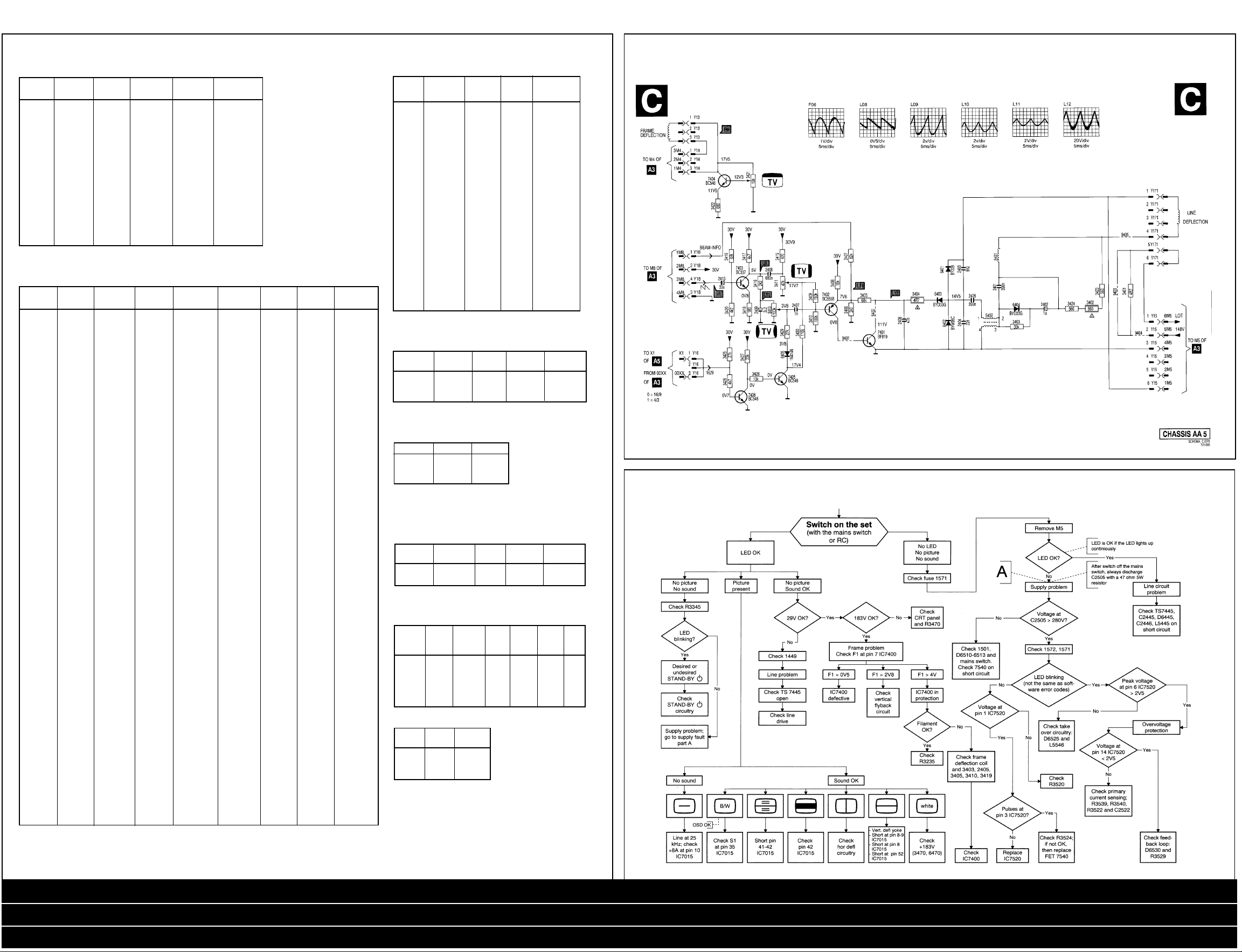
Description E/W panel 25’ and 28” AA5 AB
chassis (diagram C):
E/W correction is in this panel based on the
diode-modulator principle. This panel consists of
D6401-D6402-C2403 and C2404. By modulating the voltage on the cathode of D6402, the
current through the horizontal deflection coil is
modulated. As this is done by a parabolicshaped voltage, E/W distortion is corrected. This
parabolic-shaped voltage is derived from the
sawtooth-shaped voltage of the frame deflection. This is done by transistor T57403. E/W
correction is adapted for 4/3 and 16/9 mode by
Transistors T57405 and T57406. Coil 5401,
R3402, R3423 and R3424 are for the linearity
correction. R3402, R3423 and R3424 are for the
linearity correction. D6404, R3403 and C2402
compensate the Mannheim effect.
Transformer 5402 takes care for optimal
functioning of the diode-modulator. A too high
beam-current influences the EHT-voltage and
will in this way distortion the picture. This is
corrected by feeding the beam-info to T57402.
Adjustments:
• R3421 takes care for the vertical picture shift.
• R3411 is for adjusting the picture-width.
• R3413 is for correcting the E/W distortion.
3. Separate control panel AA5 AB chassis
(diagram D)
The separate controls panel (diagram D) is
allocated underneath the picture tube. To
release the panel first the main carrier should be
in its service position. After that the fixing screw
of the bracket holding the separate control panel
can be loosened. By then, the panel the
separate control panel can be taken out of its
bracket. In this service information the PWB and
the spare parts list of the separate control panel
is published.
Separate control panel is in functionality equal
to the controls on the main carrier. The following
selection table is valid:
1 speaker 16Ω 2 speakers 8Ω in series
1 H34 - 2H34 1H34 - 3H34 speaker right
1H35 - 3H35 speaker left
4. Difference tables
Comparing the diagrams published in the AA5
AB service manual (4822 727 20783 ... 4822
727 20788) there are several value changes for
the different screen sizes. This different values
are published in the following difference tables.
See Next Page....
Safety Parts / Electrical Adjustments ...Cont’d / Difference Tables / 110° EW Panel Diagram / Fault Finding Guide / Controls Diagram
Power Supply Diagram / Separate Control Diagram / Deflection Diagram / CRT PCB (14/15/17/21” mini neck) / CRT PCB (20/21” narrow neck)
Synchronisation Diagram / SVHS Connections Diagram / Waveforms / Text Diagram / Tuner IF Diagram / Video/Audio Diagram
Page 3
Difference tables
Diagram A1;
ITEM 14”-15”- 20”NN 21” MN 21” NN 25”-28”
17”
2505 68µF68µF68µF 150µF 150µF
2534 1nF 1nF 1nF 1nF 10nF
2535 1n5 1n5 1n5 1n5 2n2
2540 390pF 390pF 390pF 220pF 220pF
2568 1n5 1n5 1n5 1n5 470pF
3506 30R 30R 30R 30R 22R
3536 27k 27k 27k 27k 39K
3539 10R 6R8 6R8 5R6 --3540 R56 R56 R56 R47 R47
5550 60W 100W 60W 100W TRANS.11
5567 NOT NOT NOT YES NOT
5568 YES YES YES NOT YES
+86V 100V 92.5V 92.5V 82V 148V
5568 (bead 100 MHz) is instead of jumper 9568
Diagram A3;
ITEM 14” 370KRB2 15”-17” A48EEV A48ECR 21”MN 21”NN 25”&28”
2-TC38 13X31 11X19
1449 --- --- --- --- --- YES YES YES
2401 390pF 390pF 390pF 390pF 390pF 390pF 390pF mE
2404 1500µF 1500µF 3300µF 3300pµF 3300µF 3300µF 3300µF 1500µF
2405 22µF22µF4µ74µ74µ74µ72µ26µ8
2445 1nF 1nF 1n2 820pF 470pF 820pF 1n5 1n2
2446 9n1 9n1 8n2 9n1 12nF 8n2 12nF 12nF
2450 560nF 270nF 330nF 560nF 560nF 560nF 680nF 680nF
2451 10µF10µF10µF10µF10µF10µF10µF ---
2453 470µF 470µF 330µF 330 µF 330µF 330µF 470µF 470µF
2455 10nF 10nF 10nF 10nF 10nF 10nF 22nF 22nF
2456 100pF 100pF 100pF 100pF 100pF 100pF 100pF 1nF
2460 33nF 33nF 33nF 33nF 33nF 33nF 33nF 47nF
3401 3K9 3K9 3K9 2K2 2k2 2K2 1K --3403 4K7 4K7 4K7 5K6 5k6 4K7 10K 7K5
3404 2K 2K 2K7 2K 2K 4K3 4K7 4K3
3405 270R 220R 220R 180R 390R 330R 750R 150R
3406 12K 12K 12K 12K 12K 22K 22K 27K
3408 1K5 2K2 2K2 3K9 3K9 2K2 1K --3411 3R3 2R7 3R3 2R7 2R7 2R7 2R7 1R5
3412 3R3 2R7 2R7 2R2 2R2 2R2 2R2 1R5
3419 100R 100R 56R 100R 100R 100R 33R 1R2
3420 1K 1K 1K 560R 560R 910R 560R 1K
3421 39R 39R 39R 39R 39R 39R 27R 27R
3444 4K7 4K7 3K9 3K9 3K9 3K9 3K3 4K7
3449 1R 1R 1R 1R 1R 1R --- --3451 33K 33K 33K 33K 33K 33K 33K --3452 8R2 8R2 5n6 4R7 4R7 3R3 1R 1R
3454 --- 1K 1K 1K 1K 1K 1K --3457 680K 680K 680K 680K 680K 680K 680K 100K
3460 39K 39K 47K 47K 47K 47K 47K 27K
3461 --- --- 47K 47K 47K 47K 47K 56K
3462 --- --- 100K 100K 100K 100K 100K 82K
3463 --- --- 100K 100K 100K 100K 100K 82K
3464 --- --- 82K 82K 82K 82K 62K 68K
3469 4R7 4R7 4R7 4R7 4R7 4R7 --- --3470 8R2 8R2 8R2 4R7 4R7 8R2 8R2 8R2
5445 uS 4 uS 4 uS 4 uS 4 uS 4 uS 4 uSLOT S LOT110
5446 47µH47µH47µH47µH47µH47µH33µH33µH
5454 --- YES YES YES YES YES YES ---
6451 BYD33D BYD33D BYD33D BYD33D BYD33D BYD33D BYD33D --6462 --- --- BAV21 BAV21 BAV21 BAV21 BAV21 BAV21
6463 --- --- BAV21 BAV21 BAV21 BAV21 BAV21 BAV21
7441 BC639 BC639 BC639 B0639 BC639 BC639 BC639 BF819
9401 --- --- --- --- --- --- JMP JMP
9454 JMP --- --- --- --- --- --- JMP
9463 JMP JMP --- --- --- --- --- --9474 --- --- --- --- --- --- --- JMP
3PHILIPS AA5 (AB) Chassis
Diagram B2;
ITEM A48EEV A48ECR 21” 25” & 28”
13X31 11X19
1236 T1A T1A T500mA --2212 330p 330p 330p 470p
2222 330p 330p 330p 470p
2232 330p 330p 270p 470p
3238 3K3 3K3 3K3 2K2
3265 1K2 1K2 1K2 1K8
3266 56R 56R 56R 82R
3267 12K 12K 12K 15K
3275 1K2 1K2 1K2 1K8
3277 12K 12K 12K 15K
3278 56R 56R 56R 82R
3283 390R 390R 390R 560R
3287 12K 12K 12K 15K
3301 --- --- 4R7 --3303 1K2 1K2 1K2 1K8
3304 56R 56R 56R 82R
3307 --- --- 22R --5207 10µH --- --- --9207 --- YES --- ---
R3307 and R5207 are resistors parallel to jumper 9207
Diagram A4;
ITEM 14”-15”- 20” NN 21” NN 25” & 28”
17-21 MN
3340 5M6 4M7 4M7
3341 6M8 6M8 4M
9101 JMP JMP JMP ---
R3101 is a resistor parallel to jumper 9101
Diagram A5;
ITEM 25” & 28” OTHERS
3601 15K 10K
3602 3K3 8K2
3632 1K 1K
R3621 is only placed in 20”-21”NN sets.
IC7600 TMP47C....V3.0 for non ATS
TMP47C....V2.1 for ATS
Diagram A6;
ITEM 14”-15”-17” 20” NN 21” NN 25’ & 28”
21’ MN
3001 56R 39R 18R 22R
3029 1K5 1K5 --- ---
R3029 is a resistor parallel to diode 6030/
Diagram A9;
ITEM 14” 370K 15” 20” 21” 21”
RB22- 17” NN MN NN
TC38
3740 1K5 1K5 1K2 1K2 1K2 1K2
3741 1K5 1K5 1K2 1K2 1K2 1K2
3742 1K5 1K5 1K2 1K2 1K2 1K2
3749 6R8 6R8 6R8 6R8 6R8 4R7
3781 15K 15K 8K2 8K2 8K2 8K2
Diagram B1;
ITEM 14” 15-17
21” MN
2204 390pF 330pF
2217 390pF 330pF
2230 390pF 330pF
110° EW Panel Diagram
Fault Finding Guide
3469 is a safety resistor parallel to jumper 9401
3449 is a safety resistor parallel to fuse 1449
9474 is a jumper parallel to C2450
Safety Parts / Electrical Adjustments ...Cont’d / Difference Tables / 110° EW Panel Diagram / Fault Finding Guide / Controls Diagram
Power Supply Diagram / Separate Control Diagram / Deflection Diagram / CRT PCB (14/15/17/21” mini neck) / CRT PCB (20/21” narrow neck)
Synchronisation Diagram / SVHS Connections Diagram / Waveforms / Text Diagram / Tuner IF Diagram / Video/Audio Diagram
Page 4
PHILIPS AA5 (AB) Chassis
Controls Diagram
4
Power
Supply
Diagram
Separate Control PCB Diagram
Safety Parts / Electrical Adjustments ...Cont’d / Difference Tables / 110° EW Panel Diagram / Fault Finding Guide / Controls Diagram
Power Supply Diagram / Separate Control Diagram / Deflection Diagram / CRT PCB (14/15/17/21” mini neck) / CRT PCB (20/21” narrow neck)
Synchronisation Diagram / SVHS Connections Diagram / Waveforms / Text Diagram / Tuner IF Diagram / Video/Audio Diagram
Page 5
5PHILIPS AA5 (AB) Chassis
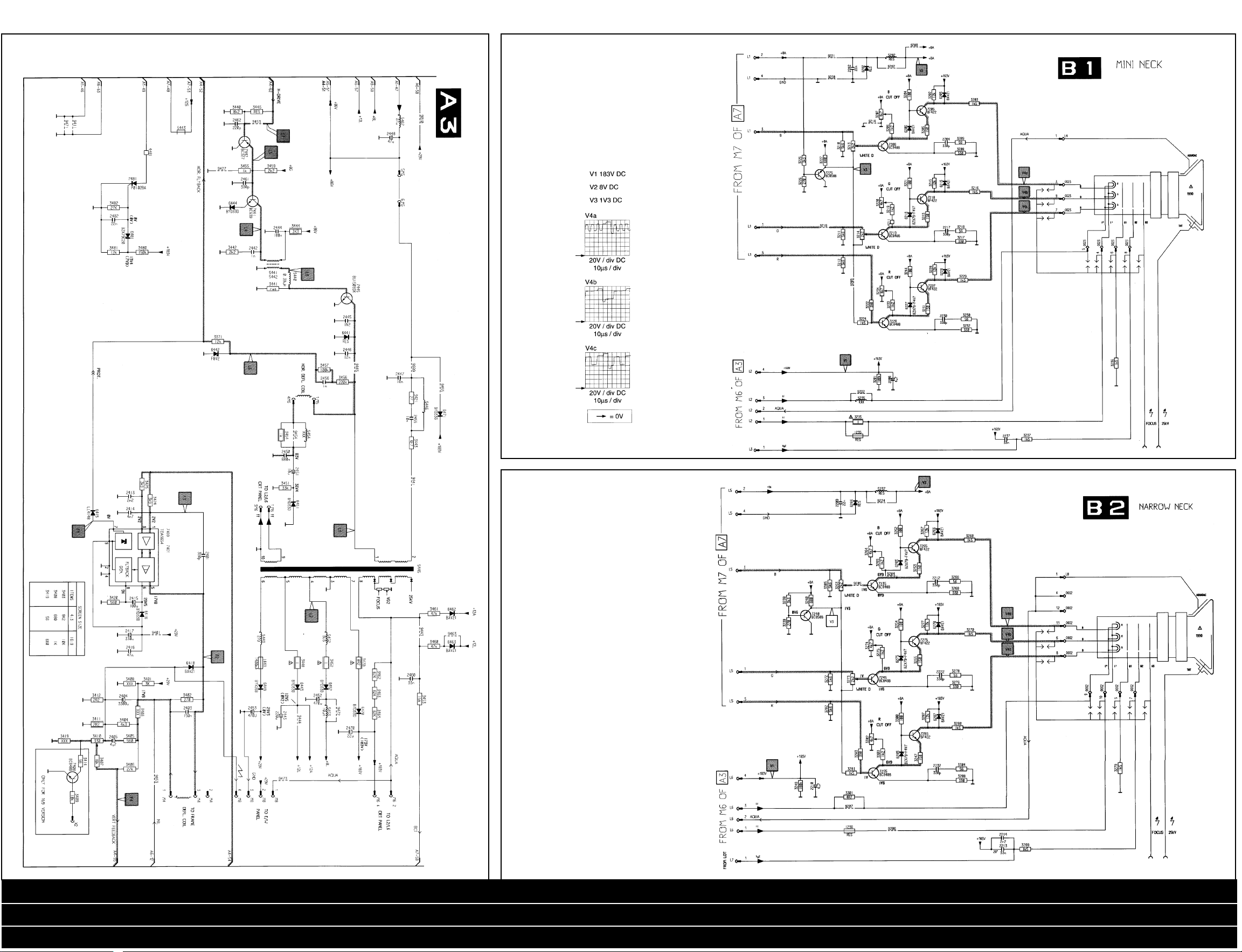
Deflection Diagram
CRT PCB
(14”,15”,17”,21”
mini neck)
Diagram
CRT PCB
(20”,21” narrow neck)
Diagram
Safety Parts / Electrical Adjustments ...Cont’d / Difference Tables / 110° EW Panel Diagram / Fault Finding Guide / Controls Diagram
Power Supply Diagram / Separate Control Diagram / Deflection Diagram / CRT PCB (14/15/17/21” mini neck) / CRT PCB (20/21” narrow neck)
Synchronisation Diagram / SVHS Connections Diagram / Waveforms / Text Diagram / Tuner IF Diagram / Video/Audio Diagram
Page 6
PHILIPS AA5 (AB) Chassis
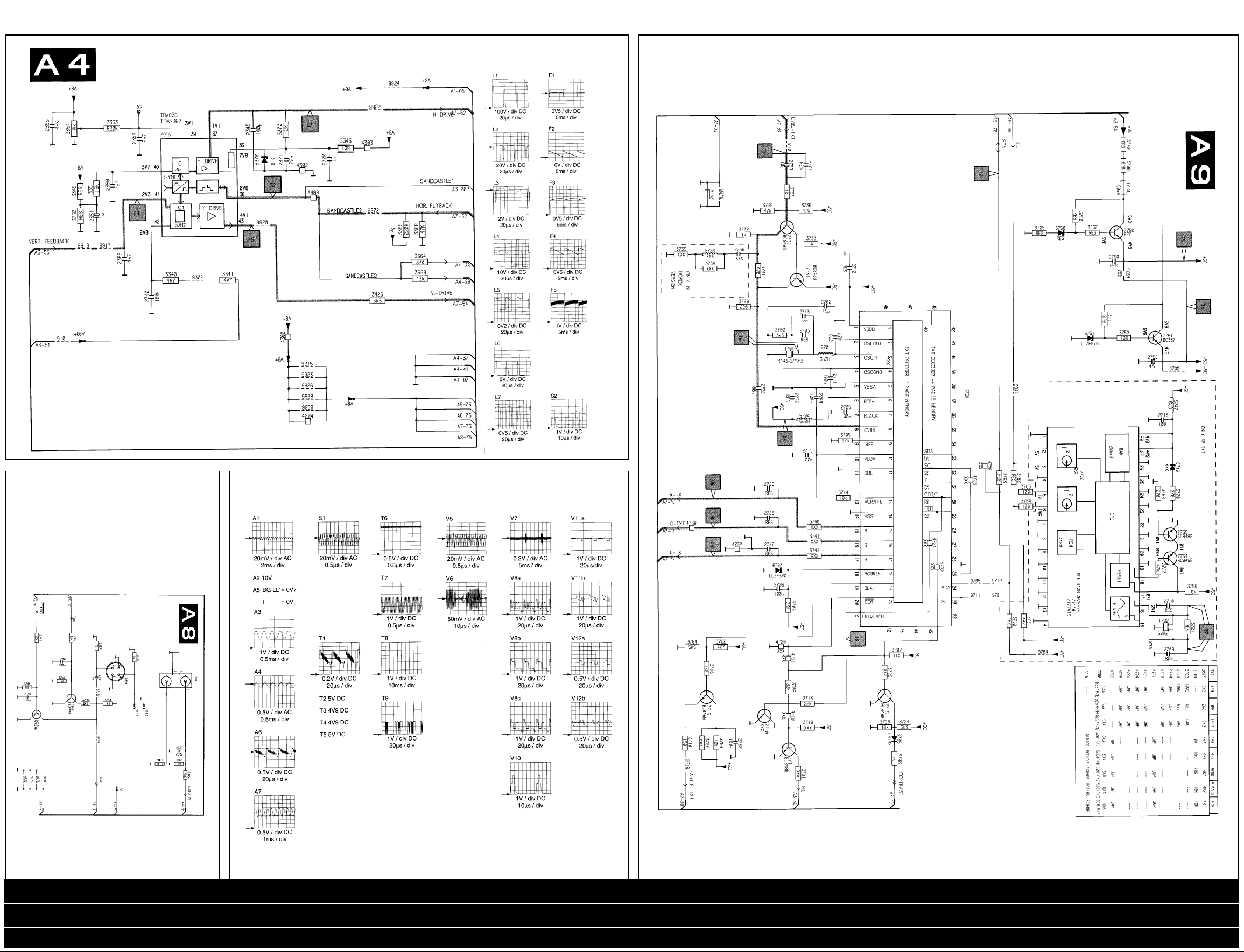
Synchronisation Diagram Text Diagram
6
SVHS
Connections
Diagram
Waveforms
Safety Parts / Electrical Adjustments ...Cont’d / Difference Tables / 110° EW Panel Diagram / Fault Finding Guide / Controls Diagram
Power Supply Diagram / Separate Control Diagram / Deflection Diagram / CRT PCB (14/15/17/21” mini neck) / CRT PCB (20/21” narrow neck)
Synchronisation Diagram / SVHS Connections Diagram / Waveforms / Text Diagram / Tuner IF Diagram / Video/Audio Diagram
Page 7
7PHILIPS AA5 (AB) Chassis
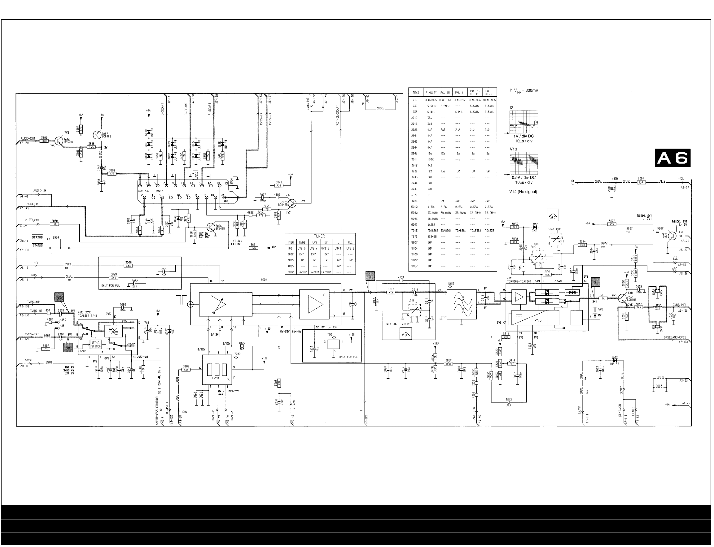
Tuner IF Diagram
Safety Parts / Electrical Adjustments ...Cont’d / Difference Tables / 110° EW Panel Diagram / Fault Finding Guide / Controls Diagram
Power Supply Diagram / Separate Control Diagram / Deflection Diagram / CRT PCB (14/15/17/21” mini neck) / CRT PCB (20/21” narrow neck)
Synchronisation Diagram / SVHS Connections Diagram / Waveforms / Text Diagram / Tuner IF Diagram / Video/Audio Diagram
Page 8
PHILIPS AA5 (AB) Chassis
8
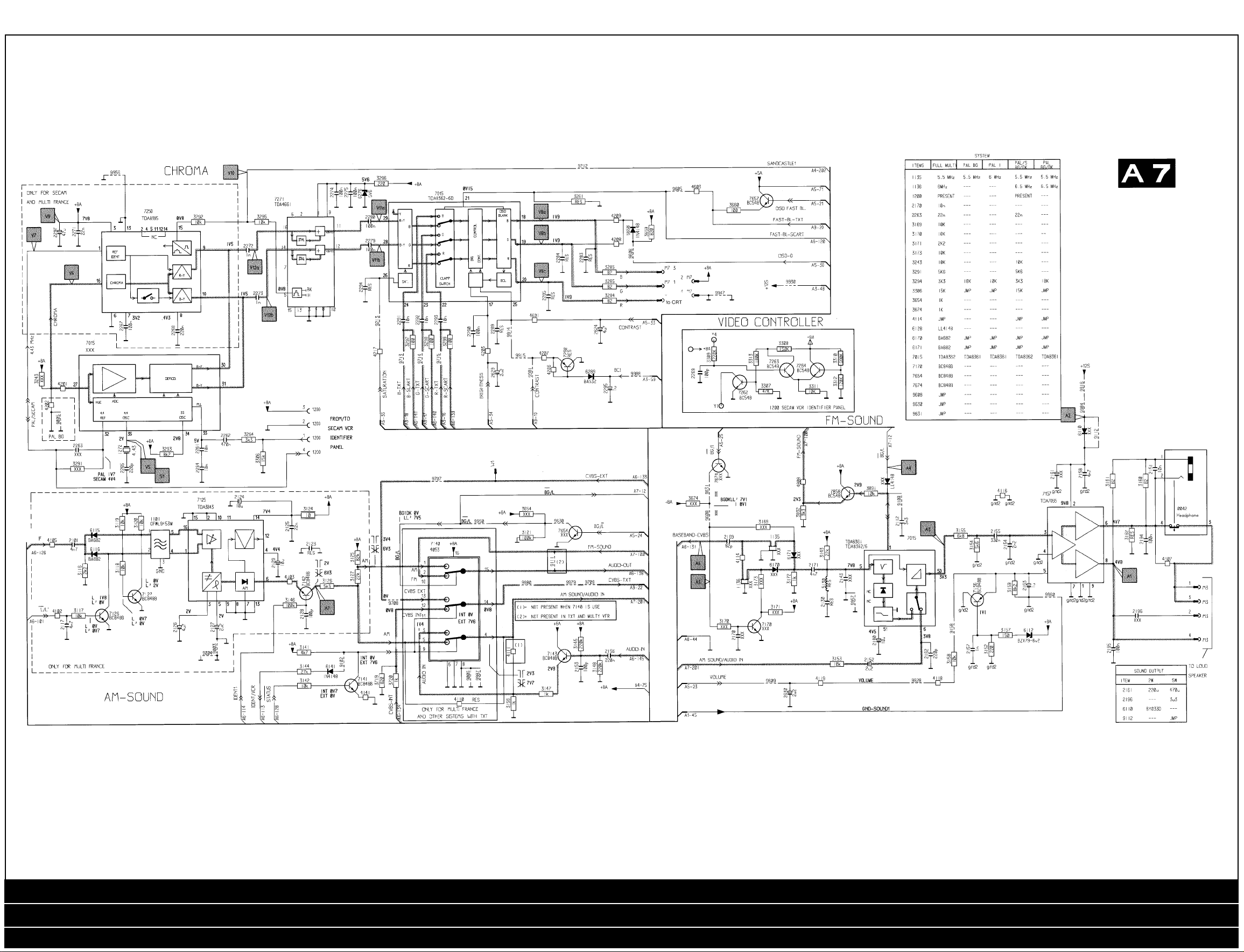
Video/Audio Diagram
Safety Parts / Electrical Adjustments ...Cont’d / Difference Tables / 110° EW Panel Diagram / Fault Finding Guide / Controls Diagram
Power Supply Diagram / Separate Control Diagram / Deflection Diagram / CRT PCB (14/15/17/21” mini neck) / CRT PCB (20/21” narrow neck)
Synchronisation Diagram / SVHS Connections Diagram / Waveforms / Text Diagram / Tuner IF Diagram / Video/Audio Diagram
 Loading...