PHILIPS A8.0A Training Manual

1
Colour television Chassis
A8.0A
Training Man ual
Contents
Introduction 2
Mechanical 3
Control 9
Power supply 24
Video processing 34
Synchronization 52
Audio processing 54
Horizontal deflection 60
Vertical deflection 80
Teletext + On-Screen Display 83
Published by TG9866 Television Service Department
Printed in The Netherlands
Copyright reserved 1998 Philips Consumer Electronics B.V. Eindhoven, The Netherlands. All rights reserved. No part of this publication may be reproduced, stored in a retrieval system or transmitted, in any form or by any means, electronic, mechanical, photocopying, or otherwise
without the prior permission of Philips
5
Widescreen view modes 89
4822 727 21613
©Copyright reserved 1998 Philips Consumer Electronics B.V. Eindhoven, The
Netherlands. All rights reserved. No part of this publication may be reproduced,
stored ina retrieval system or transmitted, in any form or by any means, electronic, mechanical, photocopying, or otherwise without the prior permission of Philips
Published by TG9866 Television Service DepartmentPrinted in The Netherlands 5 4822 727 21613
2 INTRODUCTION A8.0A
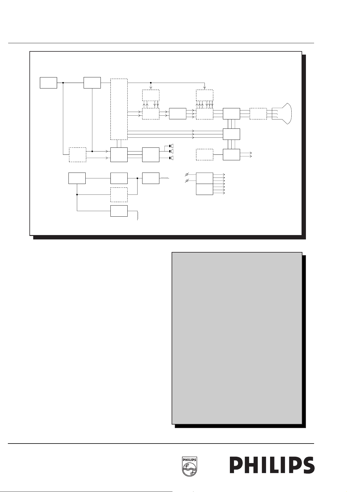
Block diagram
INTRODUCTIONBlock diagram
1125
TUNER
QSS
PANEL
7150-D
SYNC
7150-A
IF
YC PIP
PANEL
YCYC
Y/CVBS Y
IO
PANEL
SIF
SOUND
PROCES-
AM
SING
LINE
DRIVE
EW+
PANORAMA
PANEL
FRAME
AMPLIFIER
COMB
FILTER
CC
PANEL
AUDIO
AMPLIFIER
LOT
7150-0
VIDEO
PROCESSING
220V
YUV VYU
Y
U
V
R
G
B
DW PANEL
YUV
PANEL
TOP
CONTROL
PANEL
SUPPLY
SMPS
7150-C
RGB
PROCESSING
RGB
SWITCH
OSD/TXT
CONTROLS
+140
+33
+14
+8
+15
+5
+5 - STBY
RGB AMP
SCAVEM
I2C
CL 86532033_009.AI
160698
• The power is supplied by an SMPS (Switch Mode Power
Supply) creating the deflection power supply voltage (
+140V), the sound power supply voltage (+15V) and a
number of low voltages (+14V, +8v, +5v and
+5vSTANDBY).
• The controls located on the mono carrier are activated by
the keyboard and RC5 signals from the remote control receiver. The internal control is via I2C.
• TheTUNER transmits anIF video signalon 38.9 MHzto the
TDA884x (IC7150). In this IC the video processing
(PAL,NTSC and SECAM) and synchronization along with
the geometrical alignments are implemented.
• Sound decoding is performed in the sound processing part
which can be BTSC dedicated (TDA9855) ormulti standard
(MSP3410) (mono, stereo, nicam).
• In some stereo sets (mainly NICAM and FM DK) the QSS
panel (Quasi Split Sound) will be applied to improve the SIF
signal
• The CRT-panel contains integrated RGB amplifiers and
SCAVEMcircuitry. The RGB signalsare then transmitted to
the picture tube via the RGB amplifiers.
• The horizontal and vertical deflection signals (line and
frame) are amplified in the driver stages, which drive the deflection coils.
• In all sets except 21" E/W correction is needed which is accommodated on a separate panel. For 16:9 sets the panorama circuitry is also accommodated on this panel
Personal notes
A8.0A Mechanical 3
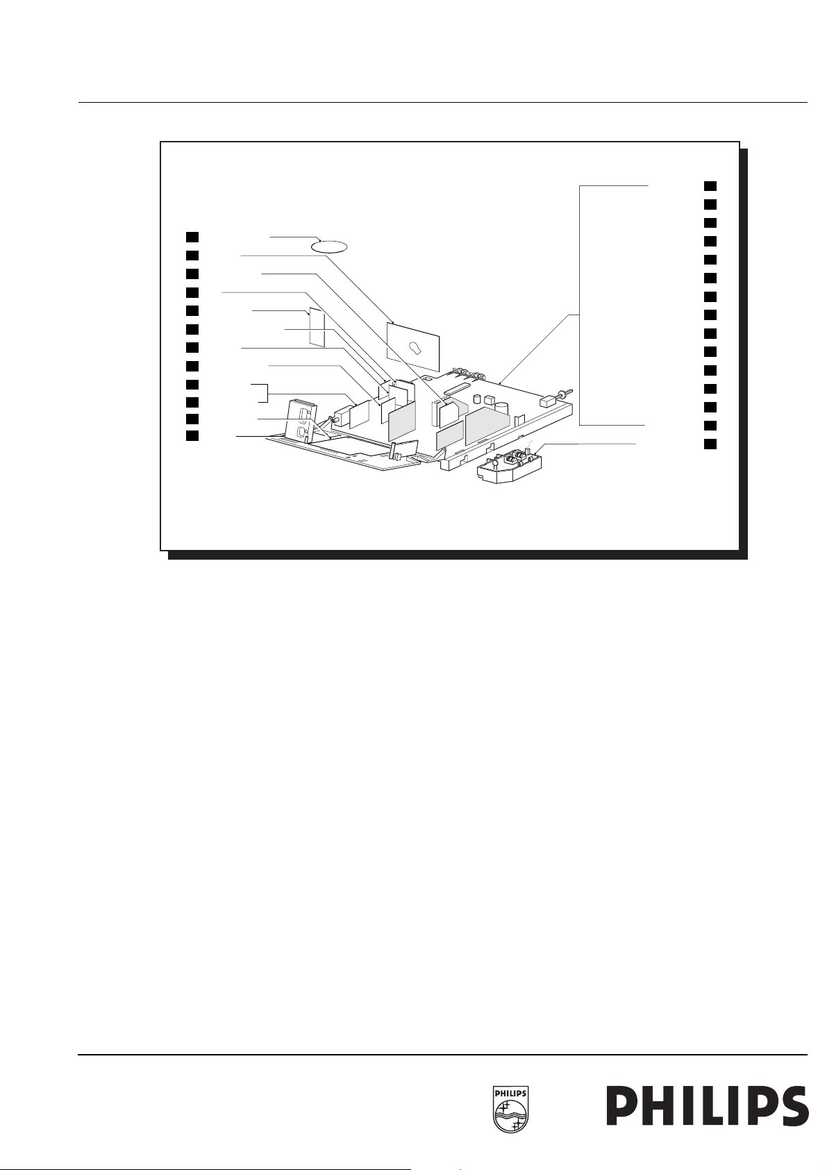
Chassis Set-up
MechanicalChassis Set-up
TOP CONTROL PANEL
N
CRT PANEL
B
EAST WEST PANEL
C
OSD
S
SIDE AV PANEL
M
Q
INCREDIBLE SOUND PANEL
R
YUV PANEL
COMB. FILTER PANEL
G
QSS-DK PANEL
J
QSS (BGLI NICAM)
I
I/O CINCH PANEL
E
PIP PANEL
T
POWER SUPPLY
HOR. DEFLECTION + LINE OUTPUT
VERTICAL DEFLECTION
TUNER + VIF
VIDEO PROCESSING
SYNC
RGB PROCESSING
CONTROLS
AUDIO PROCESSING BTSC
AUDIO PROCESSING NICAM/2CS/FM/AM
AUDIO OUTPUT
IO SWITCHING
FRONT AV
FRONT CONTROL
MAINS FILTER PANEL
CL 86532033_055.AI
A1
A2
A3
A4
A5
A6
A7
A8
A10
A11
A12
A13
A14
A15
H
180698
(The A8 has a mono carrier and panels for East West, I/O
SCART/Cinch, Side AV, QSS, Teletext, Mains filter and Top
Control.
• The mono carrier is a double sided panel with SMDs at the
solder side. It accommodates:
• the control part
• video signal processing
• source select(front/rear)
•IF
• sound processing
• audio amplifier
• horizontal and vertical deflection
• power supply
• front control(IR, LED)
• teletext in the micro-processor.
• Different panels can be placed on the mono carrier:
• QSS panel
• YUV panel
• COMB. Filter panel
• E/W Panel
• OSD panel
• incredible sound panel
• Loose panels are
• Top Control panel
• Side AV panel
• Mains filter panel
• I/O panel.
• PIP panel/ DW panel
• The CRT panel (contains the RGB amplifier circuit and
SCAVEM)
4 Mechanical A8.0A
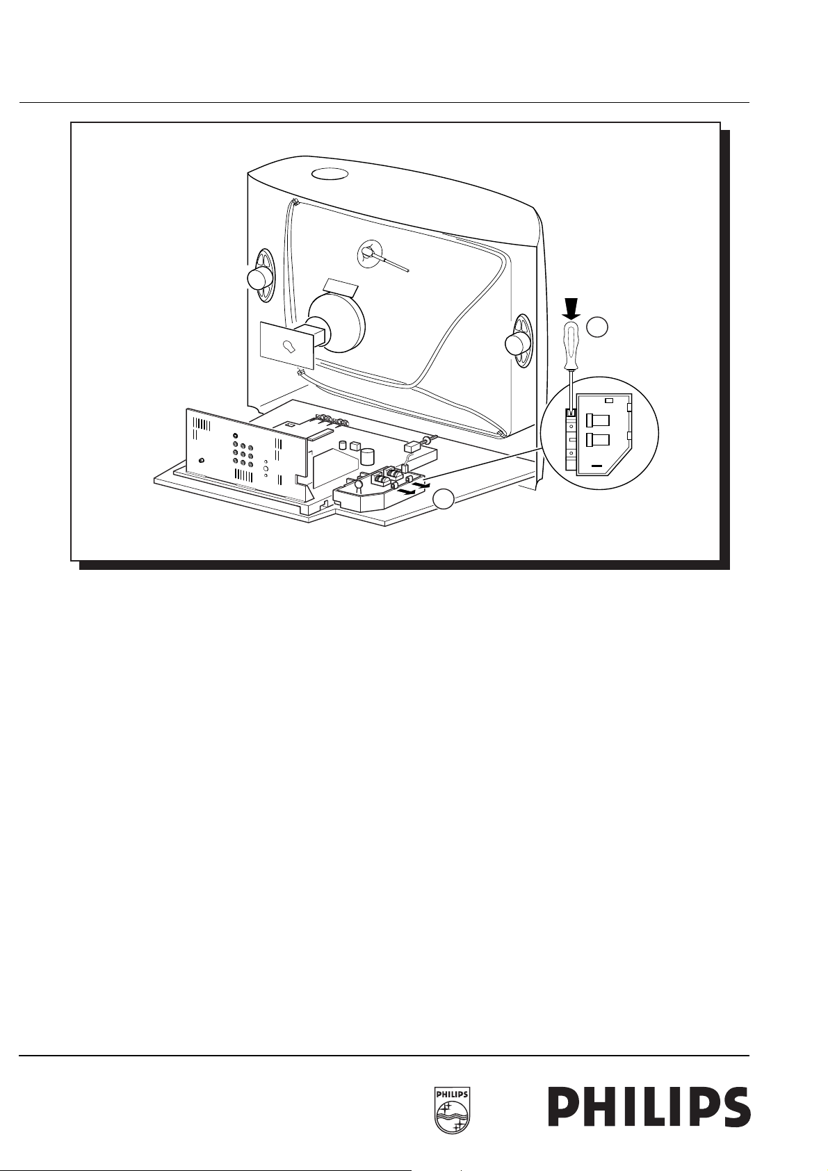
Removing the separate mains filter
Removing the separate mains filter
1
In order to remove the rear cover from the A8, all screws at the
side, the bottom and the top of the rear cover have to be removed. The screws near the I/O cinch connectors should NOT
be removed.
CAUTION!
Remember to disconnect the subwoofer connector !!
Unplug the mains cord before working on the separate mains
filter;the separate mains filter carries permanent mains voltage
(even when the mains knob is switched OFF).
Disconnect the separate mains filter panel
To disconnect the separate mains filter bracket from the chassis tray:
• firmly depress the click (with a screwdriver) in the chassis
tray (1)
• push the mains filter bracket in the direction of the CRT
2
• lift the panel from its bracket
CL 86532033_050.AI
180698
Remove the separate mains filter panel
To remove the separate mains filter panel from its bracket:
• push the 2 clips at the right hand side of the mains filter
bracket outside (2)
A8.0A Mechanical 5
Removing the chassis
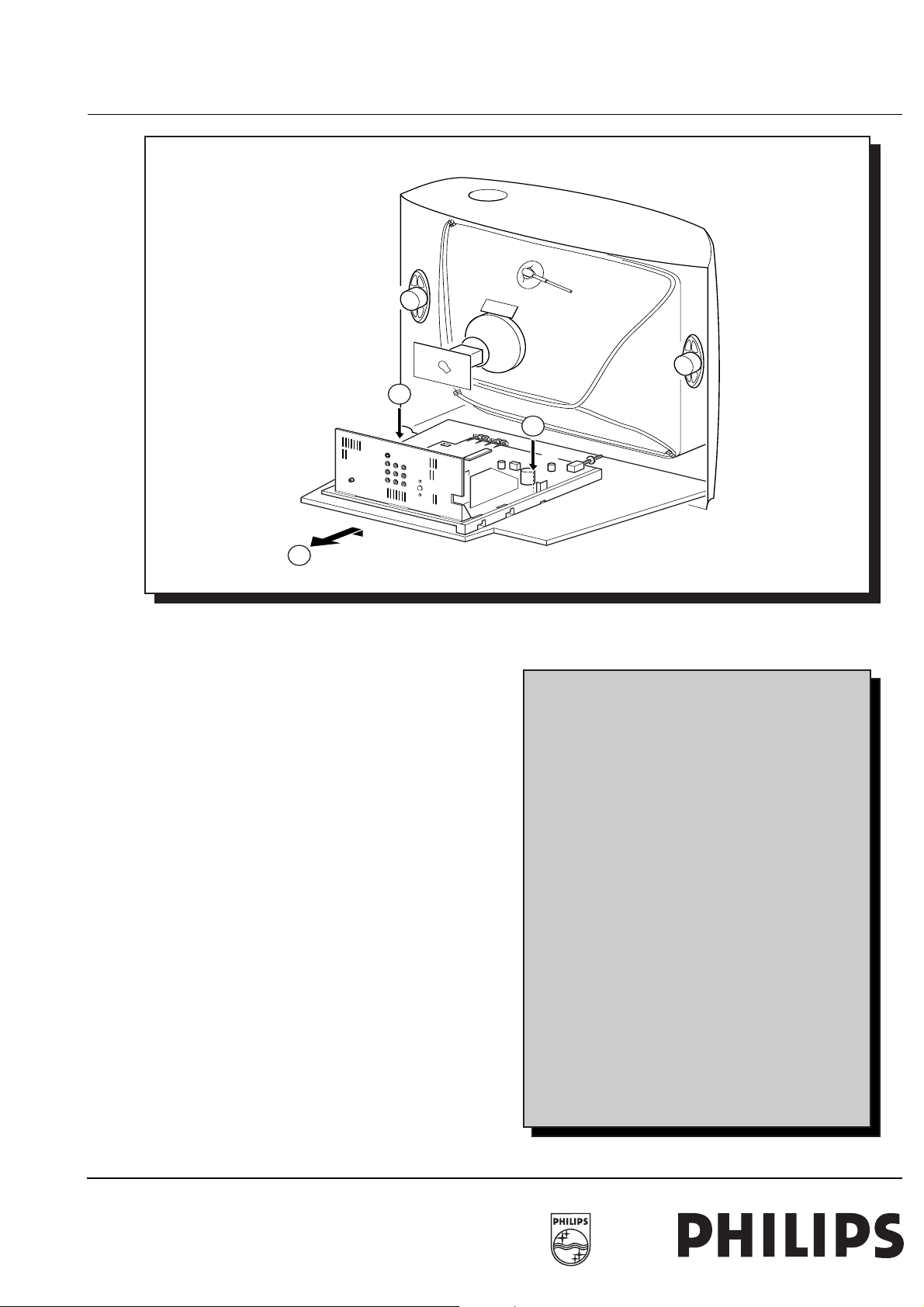
Removing the chassis
1
1
M16
2
Service position without the need for a largetable or workbench
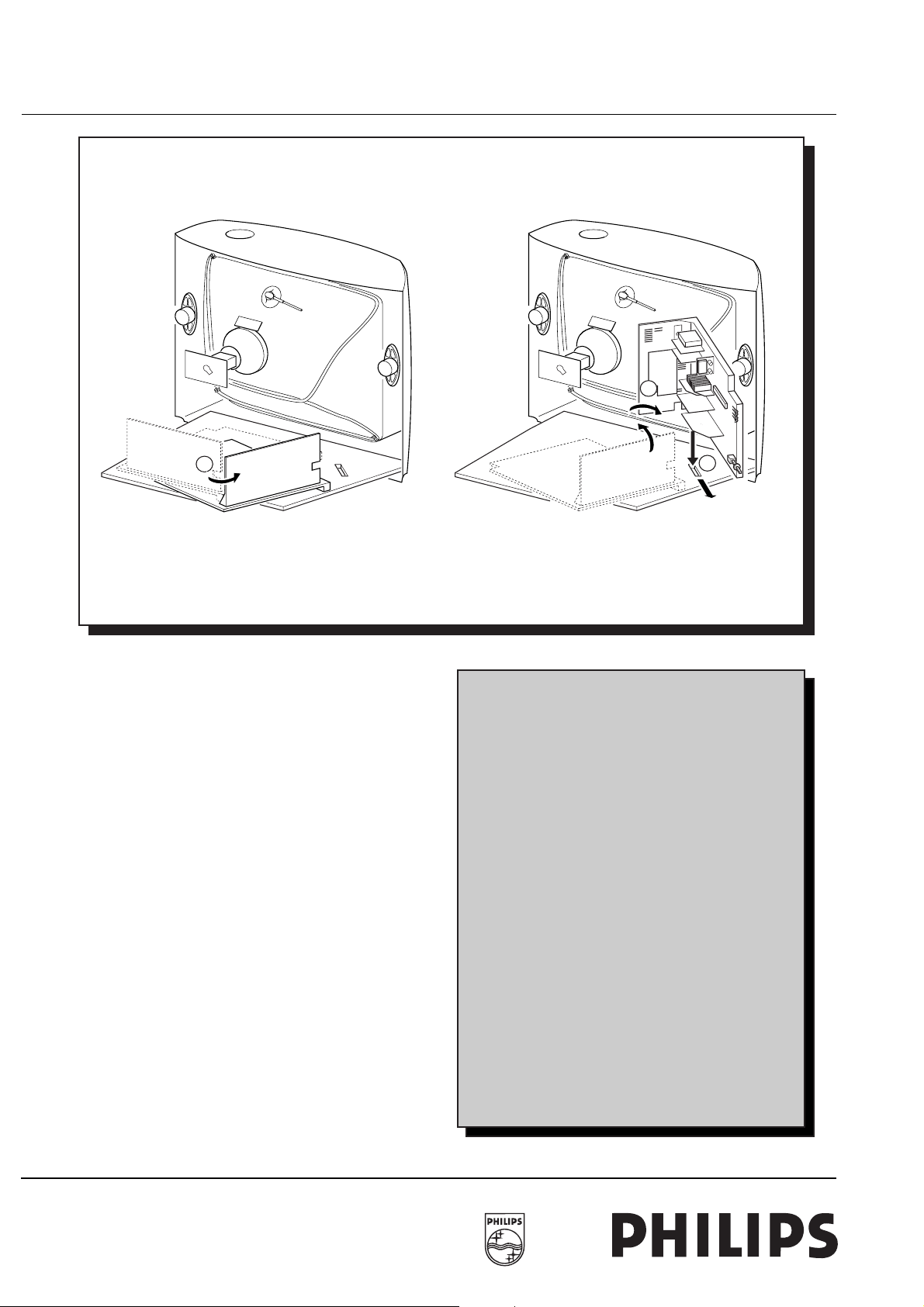
To remove the chassis tray from the cabinet:
• disconnect the degaussing coil (connector M16 on the
mono carrier)
• pull the clips (1) backwards and pull the chassis tray as indicated (2)
The chassis tray should be turned 90 degrees counter clock
wise and flipped over to access the copper side of the mono
carrier.
Personal notes
CL 86532033_051.AI
180698
6 Mechanical A8.0A
Environment independent position
Environment independent position
2
1
A
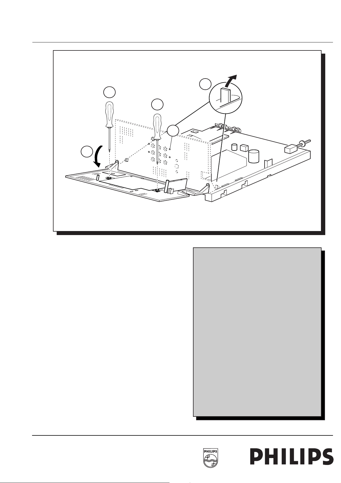
For home repair the chassis tray with mono carrier can be fixed
in the cabinet.
• turn the chassis tray 90 degrees counter clock wise (1)
• flip the tray with the I/O panel towards the CRT (2)
• press (the hook of) the chassis tray firmly into the designated hole in the cabinet bottom (3) and pull the chassis tray
forward (the speaker cables may have to be disconnected)
B
Personal notes
IO PANEL
BRACKET
3
CL 86532033_052.AI
180698
A8.0A Mechanical 7
Accessing the I/O panel
Accessing the I/O panel
1
4
4
3
2
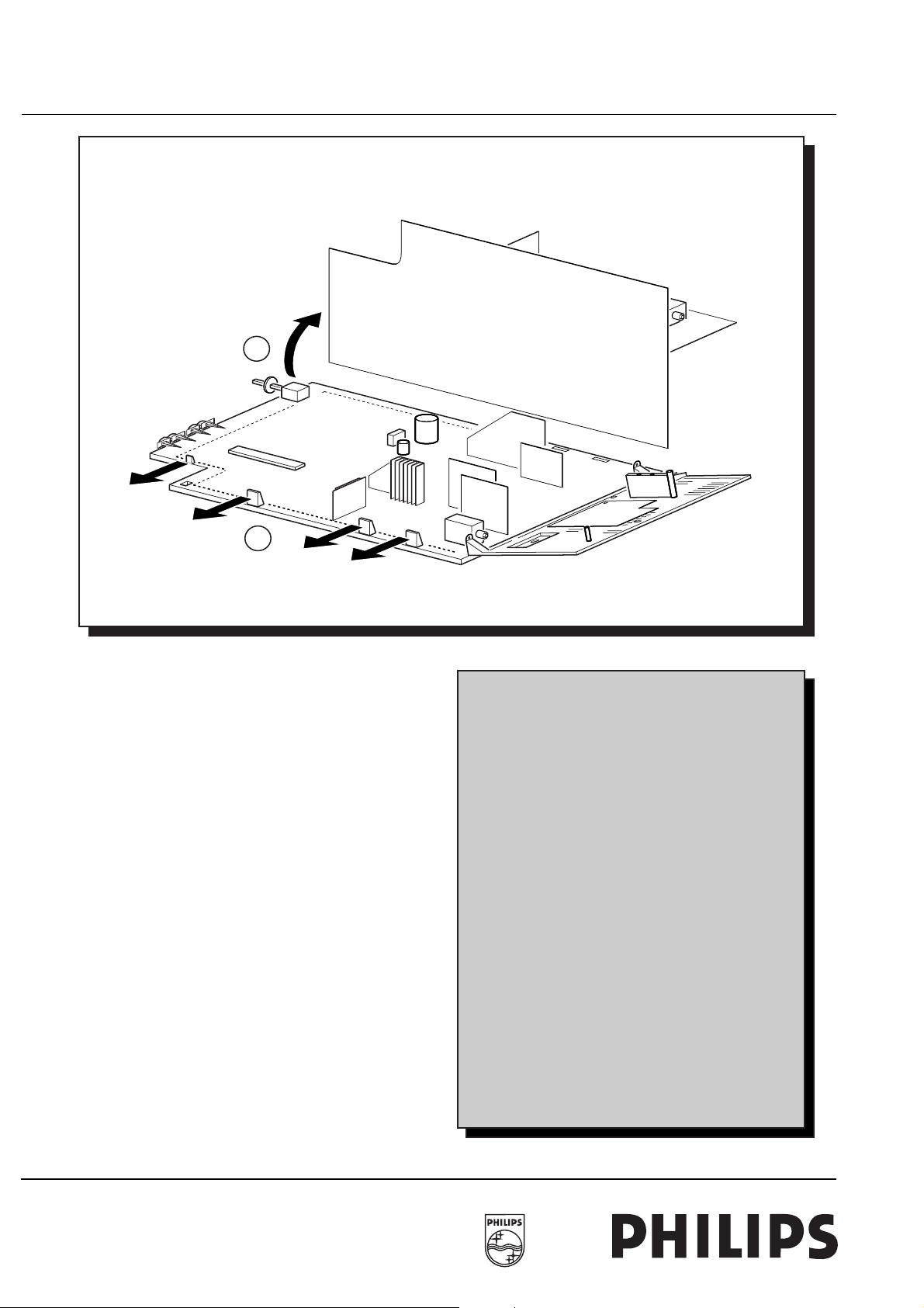
To access the copper side of the IO panel:
• push the clips (1) in the direction of the CRT (If the clips are
broken, the I/O panel can also be screwed to chassis tray)
• slide the I/O panel bracket (2) to its horizontal position
To remove the I/O panel from its bracket:
• remove the 2 screws on the connector side of the panel (3)
and (4).
(4X)
Personal notes
CL 86532033_053.AI
180698
8 Mechanical A8.0A
Repairing the mono carrier
Repairing the mono carrier
2
1
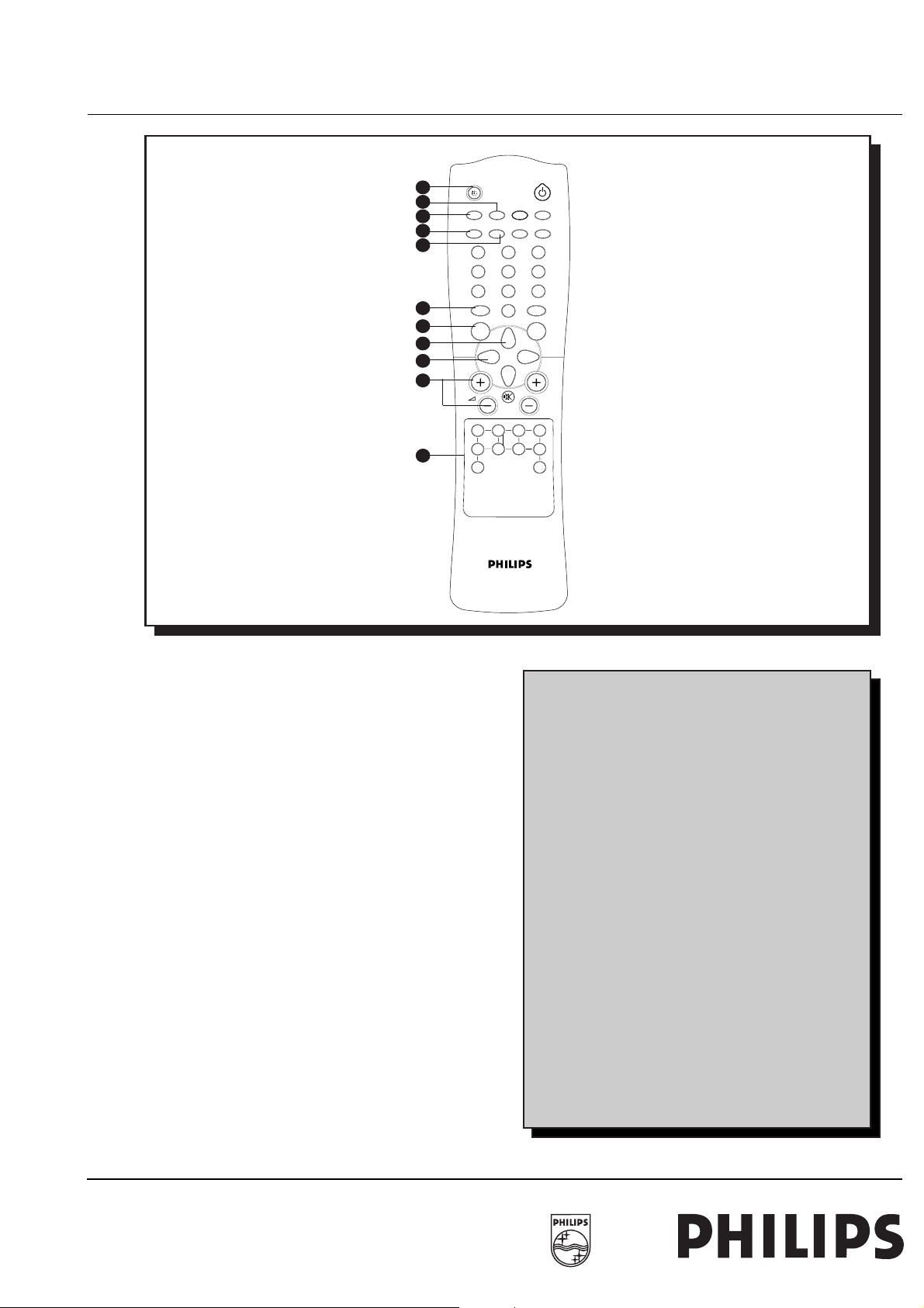
For full access to the component and copper side of the mono
carrier, it can be removed from the chassis tray.
• push the clicks of the chassis tray outwards (1)
• lift the mono carrier from the tray (2).
Personal notes
CL 86532033_054.AI
180698
A8.0A CONTROLS 9
User Menu
CONTROLSUser Menu
1
2
3
4
5
6
7
8
9
10
11
AV
INCREDIBLE
INC. SURR.
1
2
4
5
8
7
0
MENU SURF
A/CH
GAME
3
6
9
SMARTSMART
CH
The complete control of TV sets with a A8 chassis is performed
via menus. Selections within the menus are made by the arrow
keys on the remote control (cursor control).
On the remote control the "smart controls" for picture and
sound are present. Pressing one of these buttons will give a
pre-programmed change of various audio or picture settings at
the same time.
Personal notes
CL 86532033_024.AI
160698

10 CONTROLS A8.0A
Installation
Installation
Installation
Automatic
Manually
DST (RC7150)
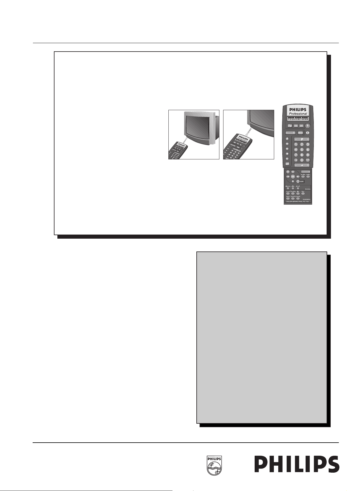
Installation of the A8 can be done via the installation menu or
via the Dealer Service Tool (DST);
1. With the Installation-menu the installation of the TV can be
performed in two ways:
• Automatic: The complete TV band is searched and all
transmitters are installed.
• Manually: The frequencies have to be given for all pro-
gram numbers.
2. With the RC7150 Dealer Service Tool (DST)
• The RC7150 can install a complete TV program table in
a single operation.
Personal notes
A8.0A CONTROLS 11
Dealer Service Tool (DST)
Dealer Service Tool (DST)
RC7150
Service Features
--Entering the Service Alignment Mode
Entering the Service Default Mode
Defined settings for tuning and control
The dealer service tool (DST, RC7150) is a remote control, especially developed for the dealer and service engineer.
• Dealer functions
– With the DST complete program tables can be transmit-
ted to the TV. 10 different tables can be stored in the
DST, e.g. for 10 different areas.
Programming tables into the DST can be performed in two
ways:
• From the TV (GFL only). If a GFL TV is installed with a complete table of program information the complete table can
betransmitted to the DST. Asuse is being made of the dealer link, the DST must be held at a short distance(within 10
cm) from the IR transmitter LED (next to the stand-by led).
• With a DST interface (22AV1376). This is a computer interface that can be used with the accompanying computer program to input tables in the computer and transmit these
tables to the DST.
• Service features of the DST for the A8
– Activating the Service Alignment Mode. By pressing the
"ALIGN" key on the DST the Service Alignment Mode
SAM) is activated.
– Activating Service Default Mode. By pressing the "DE-
FAULT" key on the DST the Service Default Mode
(SDM) is activated.
– Downloading program tables from DST into the TV.
Personal notes
CL 86532033_012.AI
160698
12 CONTROLS A8.0A
Service Default Mode (SDM)
Service Default Mode (SDM)
SERVICE DEFAULT MODE
--Shortcircuit 9040 & 9041 on the SSP
Press the "default" key on the RC7150
Tuner tuned to 475.25 MHz
All linear settings in "mid" position
Volume set to "low"
Entering the Service Default Mode (SDM):
– By transmitting the "DEFAULT" command with the RC7150
Dealer Service Tool.
– By shorting the jumpers 9040 & 9041 while switching onthe
set with mains switch.
Exiting the Service Default Mode (SDM):
– Switch the set to stand-by (the error buffer is also cleared)
Specification of the Service Default Mode (SDM)
Default values of the following must be set according;
• Tune to 475.25MHz. PAL/Secam sets
• Tune to channel 3 (61.25 MHz) for NTSC sets
• All linear setting at 50%, except volume at 25%
• Disable service unfriendly modes;
– Timer Off
– Sleeptimer Off
– Hospitality disabled
– No-ident timer disabled
– Parental lock disabled
Personal notes
CL 86532033_014.AI
160698
• The default system (for multi system sets) will be set according to the signal source input at the antenna.
A8.0A CONTROLS 13
Service Default Mode (SDM)
Service Default Mode (SDM)
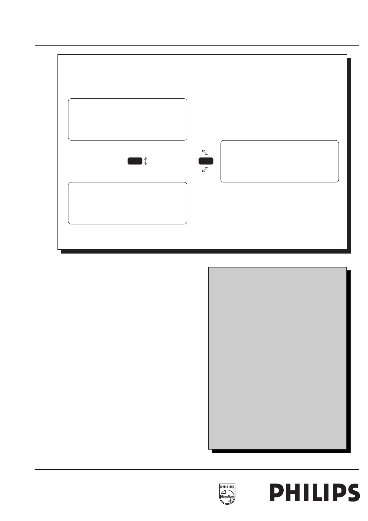
SDM Menu
SDM
ERR nn nn nn nn nn nn
+
SDM
Others features of SDM
• Error codes OSD can be switched on and off with OSD button
• Switch to user menu by pressing MENU button
• LED blinks with info of the error in error buffer
• Start channel search by pressing "P+" button on the remote
control
PICTURE BRIGHTNESS
MENU
SOUND COLOUR
FEATURES CONTRAST
INSTALL SHARPNESS
Personal notes
SAM
COLOUR TEMP
CL 86532036_003.ai
260598
14 CONTROLS A8.0A
Service Alignment Mode (SAM)
Service Alignment Mode (SAM)
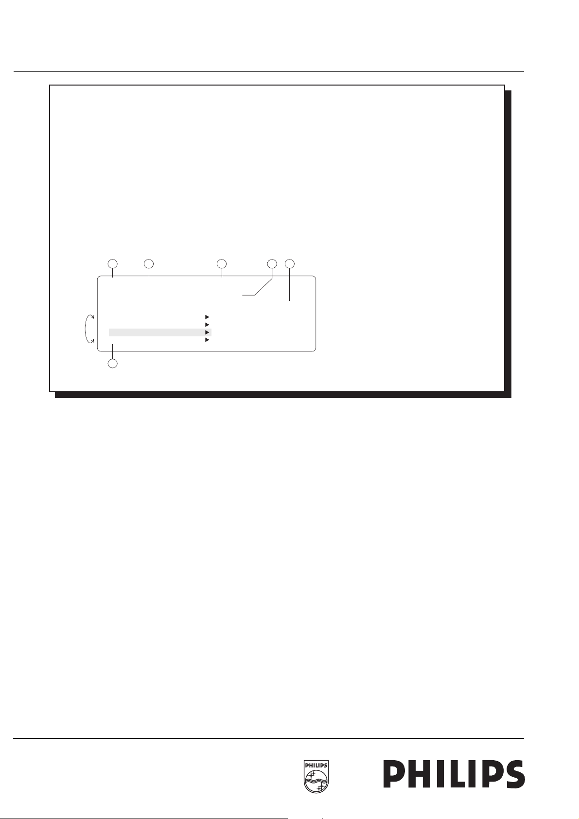
SERVICE ALIGNMENT MODE
- From SDM via "Vol +" & "Vol -"
Service Menu
1
nnnn A80EU1-1.0 5263-2-23
ERR nn nn nn nn nn nn
OP nnn nnn nnn nnn nnn nnn nnn
RELOAD DEFAULT
ERASE BUFFER
OPTIONS
ALIGNMENTS
6
2 3 4 5
Entering the Service Alignment Mode (SAM
• During normal operation and SDM by transmitting the
"ALIGN" command with the RC7150 Dealer Service Tool.
• By pressing and holding VOL+ & VOL- keys on the local
keyboard for 2 sec. while in SDM
Specification of the Service Alignment Mode
(SAM)
1. Operating hour counter ( in Hexadecimal)
2. Software version
3. Software of separate teletext controller; NOT implemented
for A/P.
4. Error code buffer (maximum the last 6 error codes
5. Option bytes (7 bytes possible
6. Sub menus
– Erase buffer
– Option codes
– Alignments and geometry information
– Reload default values
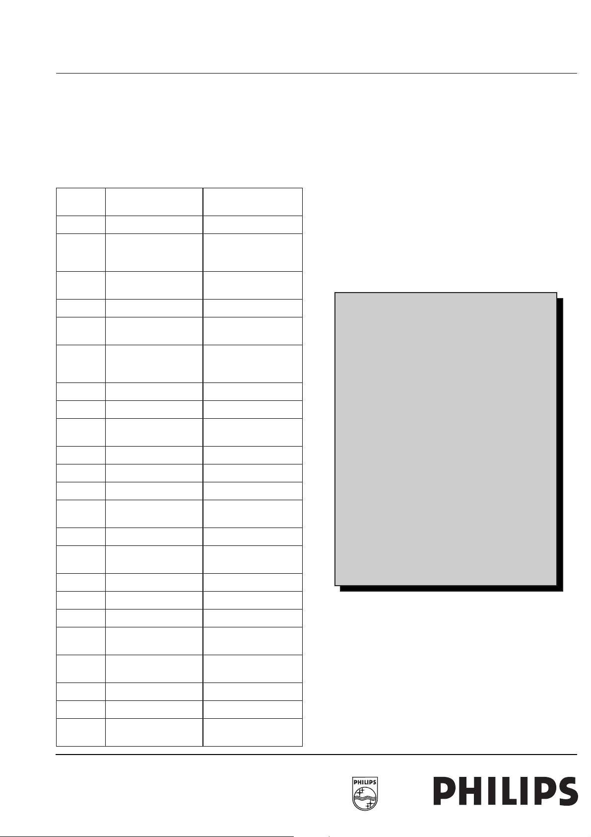
Errorcode Description ofpossible defective components 0 No
error detected - 1 EW and/or Vert protection active EW/Vertical circuit is defective 2 High beam protection active CRT
amplifier circuit or picture tube 3 Reserved 4 5V protection
active +5V supply line is low or short cuicuit 5 BiMOS s/w protectionactive or BiMOS register is corrupted IC7150 6 BiMOS
SAM
CL 86532033_039.AI
IIC error IC7150 7 General IIC bus error IICbus s/c or o/c 8
MainuP InternalRAM error IC7000 9 OSD generator IIC error
IC7101 on OSD panel 10 NVM addressing error IC7088 11
NVM IIC error IC7088 12 HistogramIIC error IC7770 on YUV
interface panel 13 Reserved 14 Sound processor IIC error
IC7430 (ITT) or IC7437 (BTSC) 15 Reserved 16 Main tuner
IIC error U1125 17 PIP processor IIC error IC7350 on PIP
panel 18 2nd tuner PIP IIC error U1126 or U1127 on PIP panel 19 EPG uProcessor/Guide Plus uProcessor IIC error
IC7007 on EPG panel
IC6 on guide plus panel 20 NV-clock IIC error IC7110 21 Reserve 22 EPG processor IIC internal RAM error IC7007 on
EPG error
160698
Exiting the Service Alignment Mode (SAM)
• The SAM will be left by the stand-by command. In case the
set is switched "off" and "on" again with the mains switch,
the set will start up in the SDM again.
Specification of the Service Alignment Mode
(SAM)
1. Operating hour counter (in hexadecimal)
2. Software version
3. Software of separate teletext controller
4. Error code buffer (maximum the last 6 error codes)
A8.0A CONTROLS 15
Service Alignment Mode (SAM)
5. Option bytes (7 bytes possible)
6. Sub menus
• Erase buffer
• Option codes
• Alignments and geometry information
• Reload default values
The error code buffer is written from left toright and contains all
errors detected since the last time the buffer is erased.
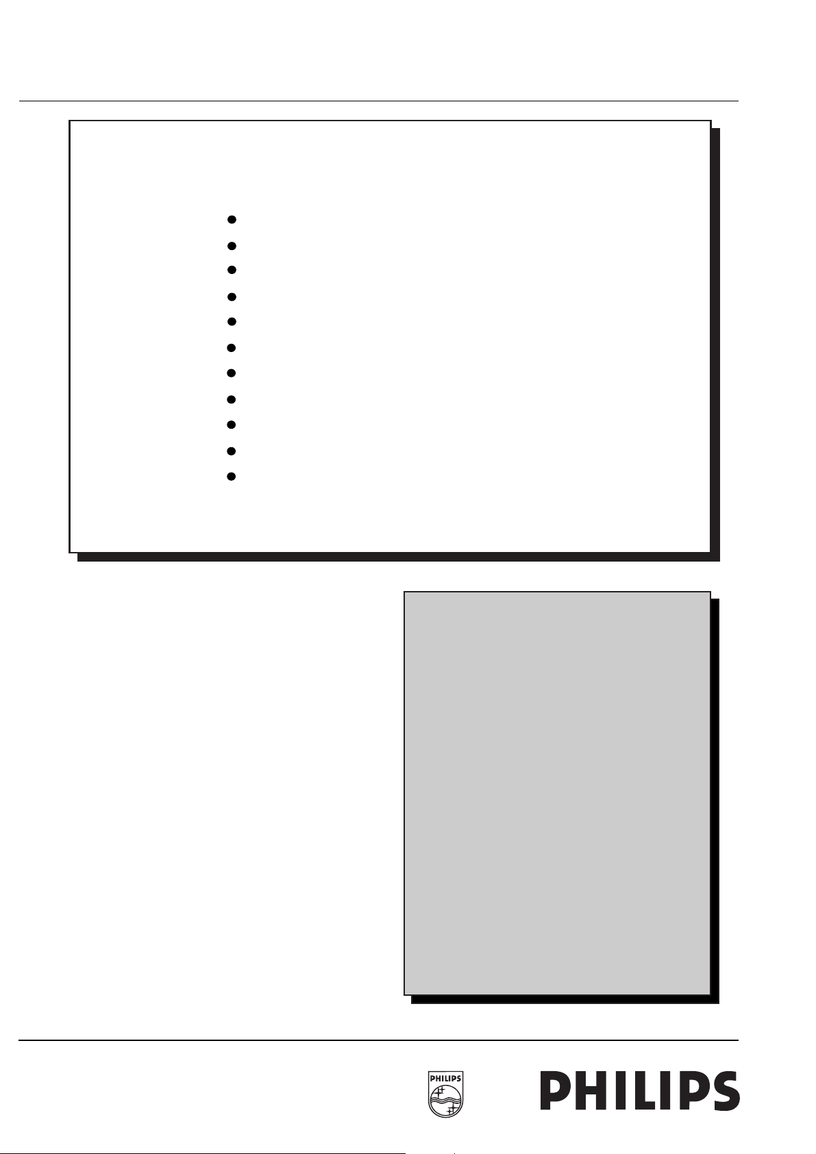
An example can be:
Error code buffer
Error code Error description Possible defective com-
ponents
0 No error detected 1 E/W and/or Vert. protec-
tion active/X-ray protection.
2 High beam protection
active
3 Reserved 4 5V protection active +5V supply line is low or
5 BiMOS s/w protection
activeor BiMOS register
is corrupted
6 BiMOS IIC error IC7150
7 General IIC error IIC bus s/c or o/c
8 Main uP internal RAM
error
E/W Vertical circuit defective,line o/p stage.
CRT amplifier circuit or
picture tube
short circuit
IC7150, + 8V supply.
IC7000
ERROR:0 0 0 0 0 0:No error code detected
ERROR:6 0 0 0 0 0:Error code 6 is last and only detected
ERROR:5 6 0 0 0 0:Error code 6 is first detected, error code 5
last detected
• The last error detected (actual) is the error at the left side
• By leaving the SAM with the "standby" function or ERASE
BUFFER function the error buffer is reset.
Personal notes
9 OSD generator IIC error IC7101 on OSD panel
10 NVM addressing error IC7088
11 NVM IIC error IC7088
12 Histogram IICerror IC7770 or YUV interface
panel
13 Reserved 14 Sound processor IIC er-
ror
15 Reserved 16 Main tuner IIC error U1125
17 PIP processor IIC error IC7350 on PIP panel
18 2nd tuner PIP IIC error U1126 or U1127 on PIP
19 EPG uP/Guide Plus uP
IIC error
20 NV-clock IIC error IC7110
21 Reserved
22 EPG processor IIC inter-
nal RAM error
IC7430 or IC7437 (BTSC)
panel
IC7007 on EPG panel/
IC6 on Guide Plus panel
IC7007 on EPG panel
16 CONTROLS A8.0A
Service Alignment Mode (SAM)
Service Alignment Mode (SAM)
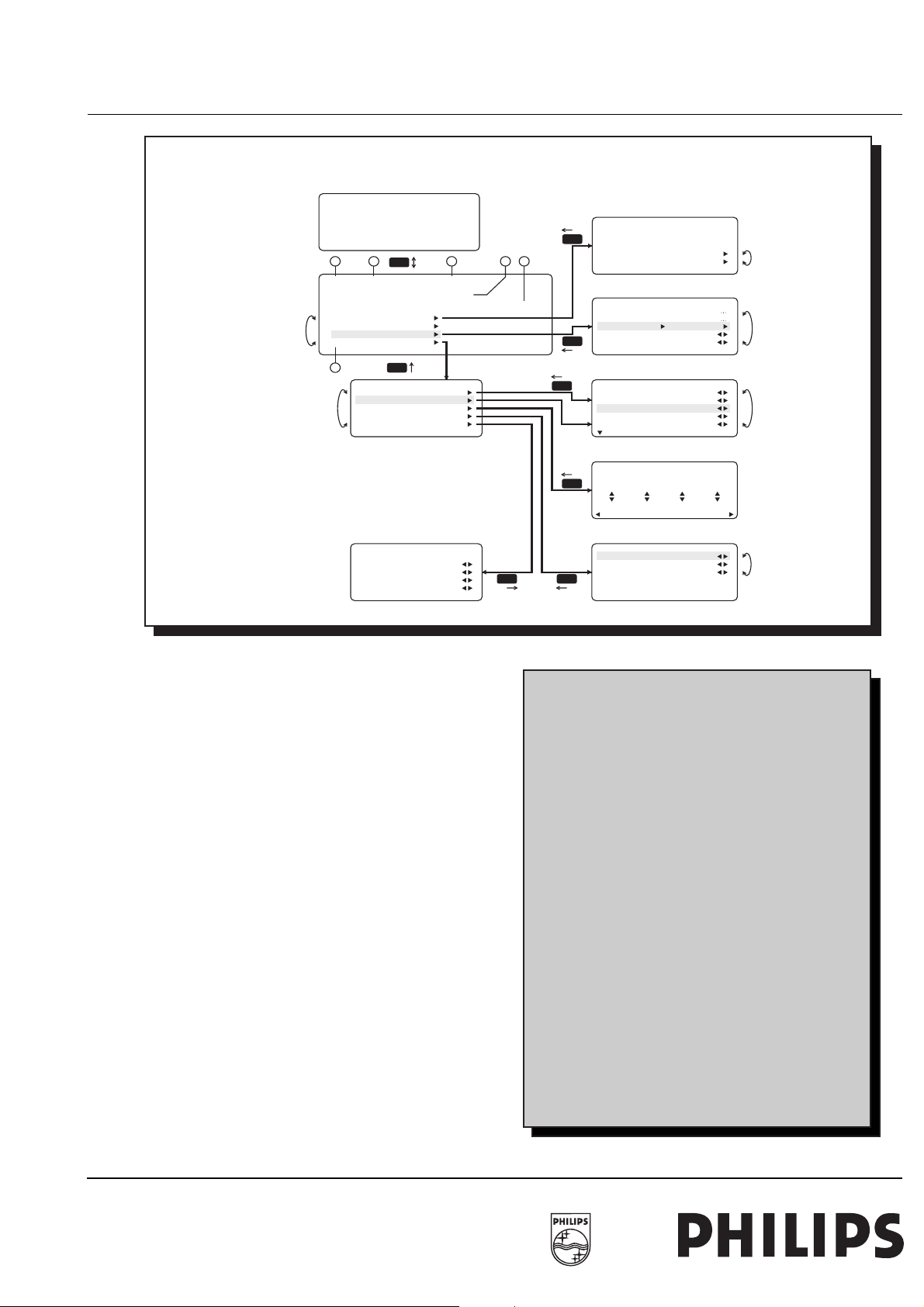
Service Alignment Mode
HORSHIFT: Horizontal shift
HORWIDTH:
SERV.BLANK: Service blanking
VERSHIFT: Vertical shift
VERHEIGHT: Vertical amplitude
VERSLOPE: Verti cal l inear i ty
EW PARABO: E-W parabola
EW TRAPEZ: E-W trapezium
EW CORNER: E-W corner
VER S-COR: Ver tical S-cor rection
VERZOOM: Vertical zoom
Alignments
• Selection of the desired alignment by the up/down cursor
• Change of the selected alignment by the left/right cursor
• The following alignments are possible (alignments for geometry are for the 4:3 picture format)
• A value between 0 and 63 can be given for all software
alignments
• Important! Any changed values will only be stored if the geometry menu is exit by pressing the MENU button.
Horizontal w i dth
Personal notes
Easy way to adjust vertical geometry (4 X 3)
1. Set vert. S-correction value to 13
2. Set vert. zoom value to 25
3. Set vert. blanking to “ON”
4. Adjust vert. slope till test pattern centre line touches the
centre edge
5. Adjust vert. shift and vert. height till best fix the screen.
A8.0A CONTROLS 17
Service Alignment Mode (SAM)
Service Alignment Mode (SAM)
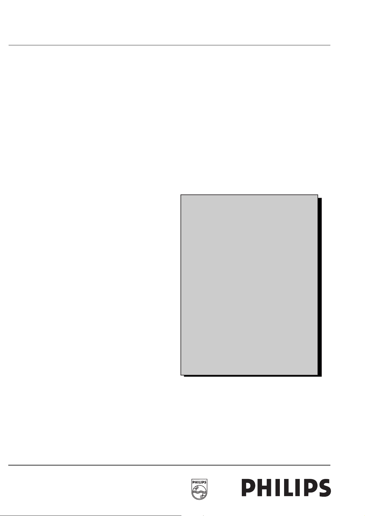
SAM Menu
nn
nn
nn
nnn
SAM
MENU
PICTURE BRIGHTNESS
SOUND COLOUR
FEATURES CONTRAST
INSTALL SHARPNESS
1
nnnn A80EU1-1.0 5263-2-23
ERR nn nn nn nn nn nn
OP nnn nnn nnn nnn nnn nnn nnn
RELOAD DEFAULT
ERASE BUFFER
OPTIONS
ALIGNMENTS
6
COLOUR TEMP
2 3 4 5
MENU
MENU
GEOMETRY
GEOMETRY SW
WHITE TONE
TUNER
BTSC SOUND
Only when HW option is present
TDA9855
LA
SA
WA
AA
SAM
MENU
LOAD NOW
DON'T LOAD
OB6
OB7
STORE
AL
MENU
AK
MENU
HORSHIFT
HORWIDTH
SERV.BLANKING
VERSHIFT
VERWIDTH
MENU
COLD Rnnn Gnnn Bnnn
IF PLL
IF PLL
AGC
MENU
AFA
AFB
nnn
nnn
ON
OFF
nnn
nnn
nnn
nnn
nnn
nnn
nnn
n
n
CL 86532036_001.ai
260598
Options
• Setting of individual options.
– Selection of the desired "option to be changed" by the
up/down cursor.
– Changeof the selectedoption (ON/OFF) by the left/right
cursor or
• By keying the decimal values in the option bytes 1~7 item
– The options are activated immediately after they are
stored and powered up.
Reload Default
By selecting LOAD NOW, the current values stored in the non
volatile memory will be over written. Caution: It is used only
when the non volatile memory data is corrupted and no other
way to recover. Default values are activated when the set is restarted
Personal notes
18 CONTROLS A8.0A
Microprocessor
Microprocessor
Introduction
Hardware and software diversity.
Europe sets:
• Master micro processor 83C770 (64k ROM).
• Slave micro processor on TEXT/EPG panel, dedicated for
EPG (Electronic Programming Guide) and Teletext decoding.
Latam and USA standard sets:
• Single micro processor 83C770 (64k ROM). Complete controls including Closed Caption decoding.
Low end USA sets:
• Single micro processor 83C570 (48k ROM).
Asia/Pacific TXT sets:
• Single micro processor SAA5297(masked) or SAA5499
(OTP).Complete controls TXT decoding.
– PN3:Pal/Multi; NO teletext; English and Arabic
– PT1:Pal/Multi WITH teletext; English, Malay and Chi-
nese
– NG1:NTSC; 2CS sound; English and Korean
– NB1:NTSC; BTSC sound; English and Taiwanese
• X = (main version number)
• Y = (subversion number)
Software identification of a separate Teletext micro controller
(DDDD E FF) (not applicable for A8.0A)
NVM
TheNVM used forstoring the default settings is ST24W16 is16
KBand is interfaced with themain micro using the S/WI2C bus.
This is to avoid any data corruption in the NVM data by controlling the Write CLock of the NVM by the main micro.
Personal notes
Asia/Pacific NON-TXT sets:
• Single micro processor 83C770 (64K ROM)
Software diversity:
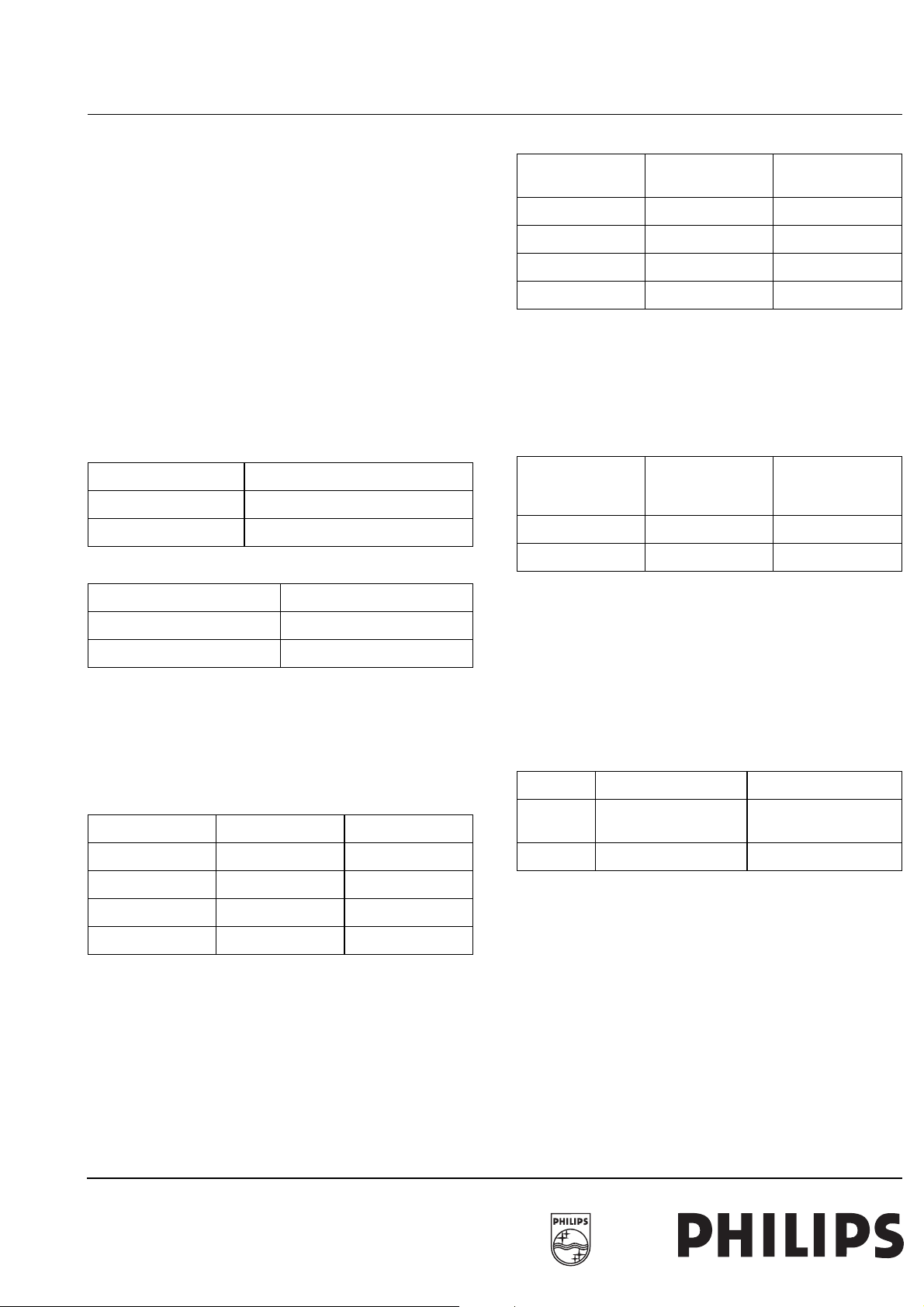
Version Region
EUROPE
A8EU1.1: Western Europe without EPG
A8EU1.2 : Eastern Europe
A8EU1.3 : Western Europe with EPG
USA
A8US1.1 : USA (all)
LATAM
A8LA1.1 : LATAM (all)
Software identification of the main micro controller (A80BBCX.Y)
• A80 is the chassis name for A8.0A
• BBC is 2 letter and 1 digit combination to indicate the software type and the supported languages:
– PN1:Pal/Multi; NO teletext; English, Malay and Chinese
– PN2:Pal/Multi; NO teletext; English and Hindi
A8.0A CONTROLS 19
Microprocessor
Microprocessor
Software control lines
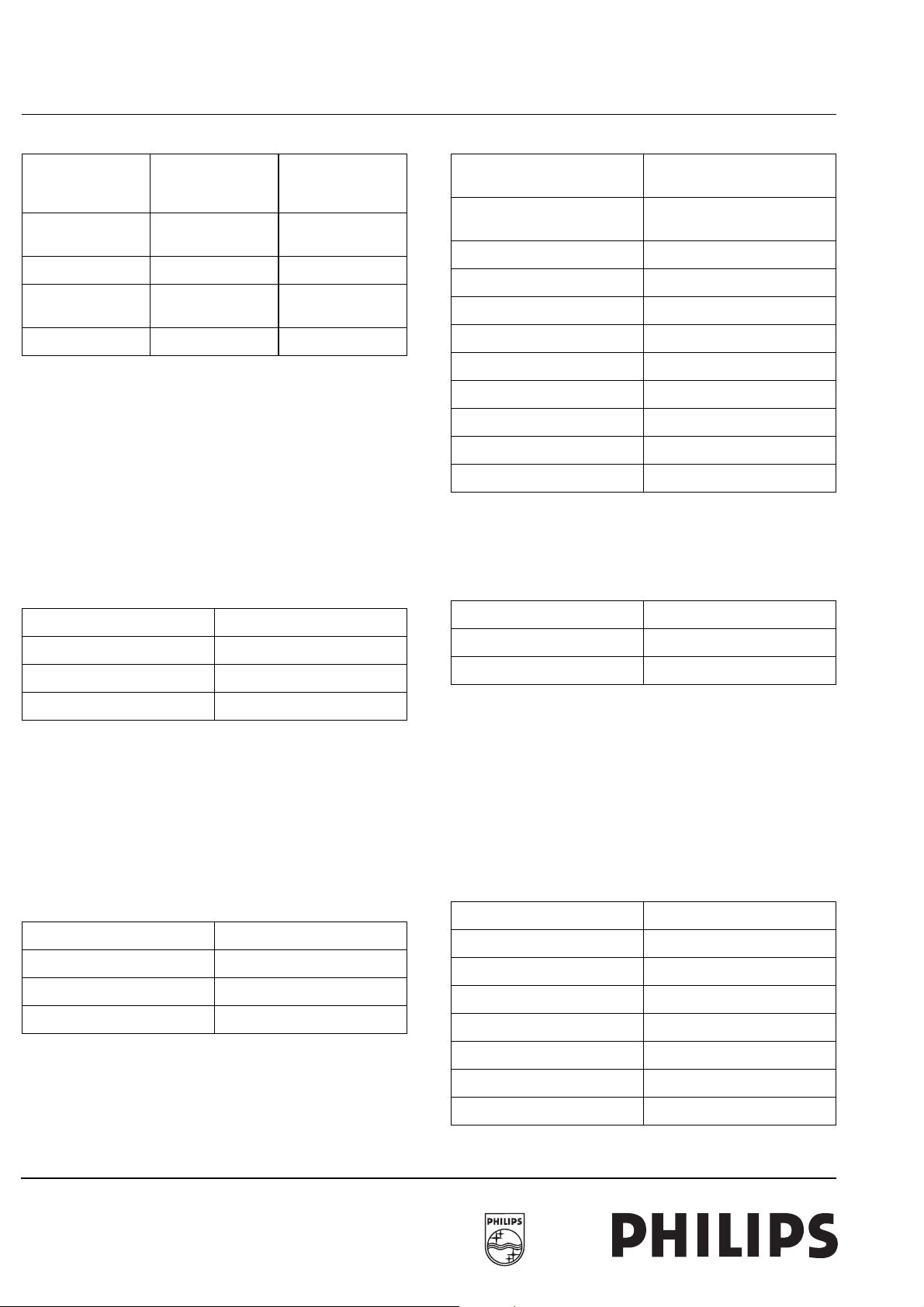
SOFTWARE CONTROL LINES DESCRIPTION for the main
micro processor
Logic 0 is : 0 V
Logic 1 is : +5V
Pin 1: PAN_SWITCH/+5V_CNTRL
OUTPUT
Activates 16:9 feature (EUROPE only)
Activates+5V supply for the PIP board (USA only)
Pin 1: PAN_SWITCH Status
0 Default
1 Super Wide Selected in 16:9 sets
Pin 1: +5V CNTRL Status
Pin 4: SEL
_PIP_FRNT_RR
0 0 REAR1
0 1 REAR2
1 0 FRONT
1 1 INTERNAL
Pin 9:
SEL_PIP_R1R2
PIP Source Selection
Pin 5: SEL_IF_TRAP_MAIN or L/L'
OUTPUT
Select the MAIN IF TRAP and Sound Traps also.
Pin 5:
SEL_IF_TRAP_MA
IN
0 ON - for NTSC M ON - for othrs
1 OFF - for others OFF - SECAM L'
A/P Europe
Pin 6: POSNEG_QSS or SEL_INCRED
1 +5V OFF
0 +5V ON
Pin 2 & 3: SYS2 and SYS1
OUTPUT
Selects the XTALS and Combfilters.
Pin 2: SYS2 Pin 3: SYS1 System
0 0 PAL M
1 0 PAL B,G,H,I,D,K
0 1 NTSC M
1 1 PAL N
Pin 4 & 9: SEL_PIP_FRNT_RR & SEL_PIP_R1R2
(valid for PIP sets)
OUTPUTS
Selects the PIP video source from rear I/O, main or front.
OUTPUT
Selects the positive and negative demodulation mode for the
QSS IC during SECAM L reception (Europe only).
Selects the Incredible Stereo feature (USA only)
Pin 6: Status - POSNEG_QSS Status - INCRED
0 POSITIVE (SECAM L/
L')
1 NEGATIVE (Others) Incredible stereo is off
Incredible stereo is on
Pin 7: SDM
INPUT
Service Default Mode is activated by shorting this pin to GND.
Pin 8 & 14: SEL_MAIN_R1R2 &
SEL_MAIN_FRNT_RR
OUTPUTS
Selects the MAIN video source from INTERNAL, FRONT or
REAR.
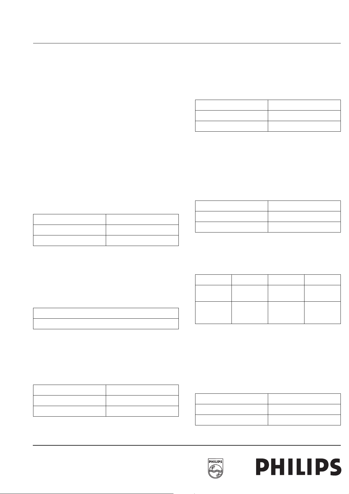
20 CONTROLS A8.0A
Microprocessor
Pin 14:
SEL_MAIN_FRNT_
RR
0 0 REAR1 (AV2/
0 1 REAR2 (AV1)
1 0 FRONT (AV3/
1 1 INTERNAL
Pin 8:
SEL_MAIN_R1R2
MAIN Source Selection
SVHS)
SVHS)
Note: For Multimedia and Institutional TV Interface pin 8 will be
configured as TV CLK.
Pin 9: STAT2 or SEL_PIP_R1R2
(valid for non PIP sets)
ADC input.
Detects the presence of SCART2 Video source (CVBS) and
also whether it is 4:3 or 16:9 video source.
Pin 9: STAT2 ADC VALUES Status - SCART2 Video
0 - 4 Internal Video
5 - 10 External 16:9
Pin 10: Function AFC_TUNE
R2
Output of Analog tp Digital Converter
0 0 - 0.5
1 - 2 1
3 - 4 1.5
5 - 6 2
7 - 8 2.5
9 - 10 3
11 - 12 3.5
13 - 14 4
15 4.5
ADC
Input DC voltage
Input
Controls the Eco Double Window.
Pin 10: SYS_ECO_DW System Status
0 50 Hz
1 60 Hz
11 - 15 External 4:3
Pin 10: STAT_EXT 1/ AFC_TUNER2/
SYS_ECO_DW
ADC input
Comparatorto sense different DC levelsfrom I/O to indicate the
presenceof an EXTERNAL SCART video sources (CVBS), 4:3
or 16:9 SCART video.
Pin 10: STAT1 ADC VALUES Status - SCART1 Video
0 - 4 Internal Video
5 - 10 External 16:9
11 - 15 External 4:3
ADC input (Valid for NTSC-M)
Indicates for the 2nd tuner PIP application for Y/C PIP and
named AFC_TUNER2.
Pin 12: POR2
Note: For Multimedia and Institutional TV Interface this pin will
be configured as DATA IN.
Pin 11: FRNT_CNTRL
INPUT ADC
Connected to the keyboard and protection line PROT_E_W.
The keys are read by applying a unique voltage.
Input DC Voltage Function ketboard read
0 Protection
1V5 Program Up
2V1 Program Down
2V7 Menu (not forLatam)
3V4 Volume Up
4V Volume Down
5V No Key Pressed
OUTPUT
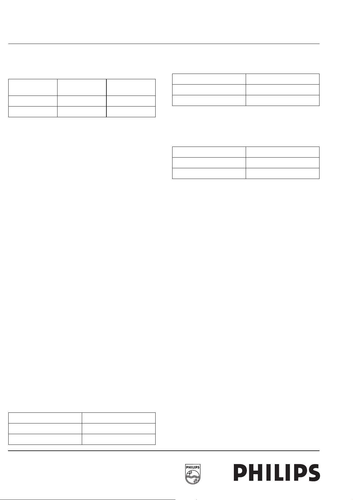
A8.0A CONTROLS 21
Microprocessor
Provides Power On Reset pulse during start-up for 2nd microp (both EPG and non-EPG boards used in Europe sets) and
GEMSTAR decoder boards used for USA sets.
For 2nd micro-p board the POR2 is high for at least 2 machine
cycles when the oscillator is running and then go back to LOW.
ForGemstar the POR2 mustgo from LOW toHIGH and remain
HIGH during start-up
Note: For Multimedia and Institutional TV Interface this pin will
be configured as DATA IN.
Pin 14: SEL_MAIN_FRNT_RR
See pin 8
Pin 15: SVHS_MODE
OUTPUT
Select/deselect the external SVHS or the CVBS inputs
Pin 15: SVHS_MODE Select
0 SVHS
Pin 18 : STAT_HP
INPUT.
To sense the presence of a Head Phone jack.
Pin 18: STAT_HP Status
0 Headphone NOT connected
1 Headphone connected
Pin 19: STBY
OUTPUT
To switch between standby and normal operation.
Pin 19: STBY TVStatus
1 In Stand-by Mode
0 in Normal Operation
1 CVBS
Pin 16: DEGAUS
OUTPUT
Controlsthe DEGAUS circuitin the Power Supply block. During
power ON this pin gives low going pulse for 2 seconds.
Pin 16: DEGAUS
'0' for 2 seconds and then goes to '1'
Pin 17: AMP_MUTE1
OUTPUT
Mutes the Audio Output Amplifier
Pin 17: AMP_MUTE1 Status
0 MUTE OFF
1 MUTE ON
Pin 20: LED
OUTPUT
Pin 20 Europe AP/Latam USA
0 LED brighter
= Standby
1 LED dimmer
= normal operation
LED lighted =
Standby
LED OFF =
normal operation
LED lighted =
normal
LED OFF =
Standby
Pin 21 SAA5297/P83C770: SEL_GAIN_SPLIT/
SEL_TUNER1_2
OUTPUT
Selects the gain of the antenna splitter of the 2nd tuner for PIP
(A/P and LATAM sets only).
Pin 21: SEL_GAIN_SPLIT Attenuation
0 OFF
1ON
OUTPUT
22 CONTROLS A8.0A
Microprocessor
Selects between the MAIN tuner 1 and MAIN tuner 2. (USA
and 2 Tuner PIP sets only).
Pin 21:
SEL_TUNER1-2
0 Not selected Selected
1 Selected Not selected
Tuner 1 Tuner 2
Pin 30 P83C770: RMT_LOC_DATA
OUTPUT
Signal: DATA to the REMOTE LOCATOR circuit (USA only),
others this pin is pulled to “high” via 3063.
Pin 46 for SAA5297 and P83C770 :
WRITE_CTRL
OUTPUT
Selects the global write protection control of the EEPROM
(IC7088).
Pin 52 of P83C770 : FFBL_EXT/4_NORMA_SEL
Pin 52: FFBL-EXT Status
0 RGB present on the SCART
1 No RGB on the SCART
ForLATAM setsthis pin isused toselect the respective crystals
4 or 2/3 Norma sets. This is configured by hardware as LOW or
HIGH depending on the crystals connected to the BiMOS.
Pin 52: 4 NORMA_SEL Status
0 Selects 4 Norma
1 Selects 2 or 3 Norma
OTHER PIN DETAILS
Pin 13: Ground
Ground line for digital circuits for SAA5297 and P83C770
Pin 47 SAA5297/P83C770 : SCL_EEPROM
Clock output EEPROM I2C bus.
Pin 48 SAA5297/P83C770 : SDA_EEPROM
Data in - output EEPROM I2C bus.
Pin 49 SAA5297/P83C770 : SCL
Clock output of master I2C bus.
For a survey of all connected ICs to this bus see the diagram
"I2C overview" in the service manual.
Pin 50 SAA5297/P83C770 : SDA
Data in - output of master I2C bus.
Pin 51: RGB_KILL
(Valid for SCART sets !)
Output
Pin 22: VSSA (For SAA5297 and P83C770 )
Ground line for analog circuits
Pin 23: Ground
Input
CVBS from which closed caption for USA/LATAM or TEXT
data for EUROPE/AP is to be extracted. A positive going 1V
(peak-to-peak) input is required.
Pin 24: STN For P83C770 and CVBS1 for SAA5297
For SAA5297 this data slicer decoupling capacitor input, connect to VSSA via a 100 nF capacitor (C2054).
Pin 25: BLACK & BLK (For SAA5297 and P83C770 )
CVBSsignal black level reference,connected to VSSA via100
nF capacitor (C2055).
Pin 26: IREF (For SAA5297 and P83C770 )
CVBS signal reference current input, connect to VSSA via a
27K resistor (R3058)
Pin 51: RGB_KILL Status
0 Default
1 Kill External RGB
Pin 27: TEST (For SAA5297 and P83C770 )
This pin is connected to +5V via 10 K Ohms resistor (R3060)
Pin 28: TEST (For SAA5297 and P83C770 )

A8.0A CONTROLS 23
Microprocessor
This pin is connected to Digital gnd for SAA5297. For P83C770
this pin is pulled to high via 3061.
Pin 29: TEST (For SAA5297 and P83C770 )
This pin is connected to +5V via 10 K Ohms resistor (R3062).
Pin 31: RGBREF & REFH (For SAA5297 and P83C770 )
For SAA5297 this is the DC input voltage to define the output
HIGH level on the RGB pins,
For P83C770 this is the data slicer reference high capacitor inputconnectedtoVSSAvia100nFcapacitor(C2070).
Pin 32 to 35 (For SAA5297 and P83C770 ): FBL, R, G and B
Outputs 'RED', 'GREEN' and 'BLUE' deliver the colour components for the OSD, while output 'Blanking' is used as a fast
blanking signal to insert R, G and B signals in the television picture. The output polarity of all four pins is active high.
Pin 36: HSYNC for OSD /TXT (For SAA5297 and P83C770 )
This signals is derived from the deflection part to get a stable
OSD picture on the television screen. The 'HSYNC' pins is
supplied with active low horizontal sync pulses (polarity is software programmable).
Pin 37: VSYNC for OSD/TXT (For SAA5297 and P83C770)
This signal is derived from the deflection part to get a stable
OSD picture on the television screen. The 'VSYNC' pin is supplied with active low vertical sync pulses (polarity is software
programmable).
Pin 38 for P83C770 & SAA5297 : VDDA
This pin is connected to +5VA
Pin 39: VDDT for SAA5297 & VDD_P P83C770
For SAA5297 this pin is connected to +5V Teletext power supply.
This is XTAL oscillator OUTPUT pin. All internal timing of the
micro-controller is derived from this oscillator The oscillator frequency has to be 12MHz.
Pin 43 for SAA5297 and P83C769 : POR
'POR' is used to reset the micro-controller after a power-on reset. This reset signal has to be HIGH until a stable 5V supply
voltage is available and then it goes LOW. Also when the supply voltage drops below the minimum required voltage the micro-controller has immediately to be reset via pin 'POR'.
Pin 44 for SAA5297 and P83C770: VDDM
For SAA5297 and P83C770 this pin is +5V micro-controller
power supply.
Pin 45 for SAA5297 and P83C770 : RC-5
This input pin is connected to an RC5 remote control receiver(TFMS5360). The input should be high when no remote control signal is received.
Pin 52 for SAA5297 and P83C770: N.C
For SAA5297 and P83C770 this pin can be used as an I/O port
and is not connected. Pulled to “high”.
Some hints on problem solving
No LED or IIC activity - Check for the +5V_STBY and the POR
pulse
Set always on standby - Check +8V of BiMOS
LED Blinking - The set may be on protection. Check pin 11
No LED blinking to RC5 - Check NVROM
No OSD/TXT - Check H sync on pin 36
No TXT- Check CVBS_TXT on pin 23 and +5V at pin 39.
For P83C770 this pin is the Digital periphery power supply.
Pin 40: OSCGND for SAA5297 & VSS_D for P83C770
For SAA5297 this pin is connected to crystal oscillator gnd.
For P83C770 this pin is the Digital Ground.
Pin 41 for SAA5297 and P83C770 : XTALIN
This is XTAL oscillator INPUT pin
Pin 42 for SAA5297 and P83C769 : XTALOUT
24 POWER SUPPLY A8.0A
Degaussing
POWER SUPPLYDegaussing
PTC
3908
*
+t
ZPB
2
3906
*
PTC
1
9950
*
1
3
2
M16
TO DEGAUSSING
COIL
}
0132
2
1
TO F15
OF MAINS
FILTER
2
{
1
M15
2M2
3950
4
3
9999
*
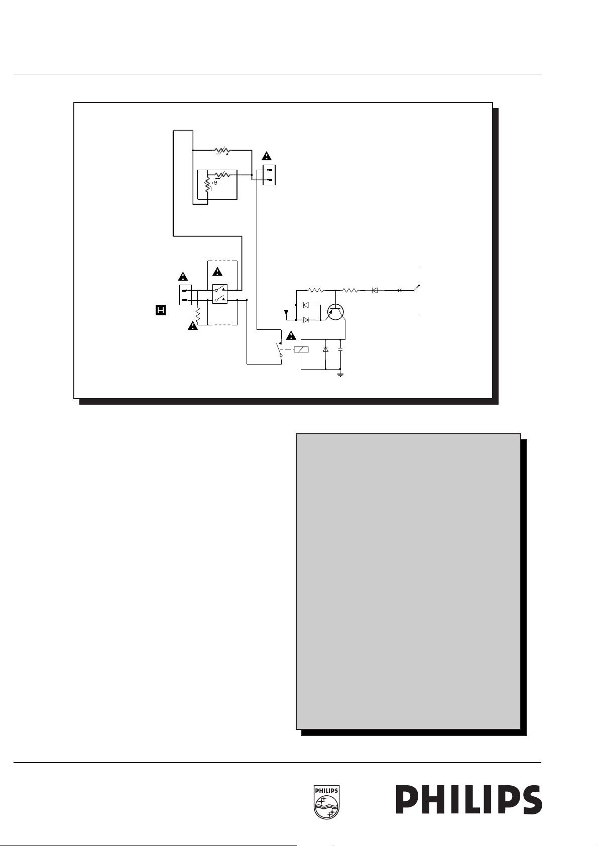
The degaussing circuit is activated whenever the TV set is
turned on. So from normal off to on and from stand-by to on the
degaussing circuit is activated. During start-up the signal degaus (A8-05) is high which blocks TS7900. After start-up of the
uPthe signal degaus (A8-05) becomeslow for 3 seconds which
forces TS7900 in conduction. Now the +13V is put on the coil
of the relay and switch G5P-1 is closed. The degaussing current passes through the degaussing coil. After three seconds,
DEGAUS goes high, 7900 turns off , 1901is de-energised and
no current passes through the degaussing coil at normal operation due to the fact that switch G5P-1 is opened. PTC 3906 is
present in 220V sets and PTC 3908 is present in 110V sets.
BZX79-C3V3
+13V
6920
1N4148
6935
G5P-1
14
23
6992
13V4
1N4148
6904
13V4
22n
3911
4K7
BC557B
7900
0V
2908
BZX79-C9V1
RELAY
SWITCHER
10K
3910
1901
Personal notes
DEGAUS
A8-05
CL 86532033_011.AI
160698
A8.0A POWER SUPPLY 25
General information
General information
CL 86532033_049.AI
160698
26 POWER SUPPLY A8.0A
General information
The A8 power supply is a Switch Mode Power Supply(SMPS)
with minimum voltage switch. The topology is a flyback converterwith primary current sensing, secondaryvoltage sensing and
mains input Voltage measuring. The power supply is built with
IC 7902 which has a built-in MOSFET and control circuit. The
frequency ranges for normal operation are 25kHz to 130kHz
(full range) and 40kHz to 130kHz (single range and 120V).
The SMPS works in discontinuous mode, so with a T-on, T-off
and a Tdead. The FET is switched on during T-dead when the
voltage at the drain of the built-in FET (IC7902 pin 3) is minimal
due to oscillation of C2913 and the primary inductance of
T5912. This is reducing the switching losses.
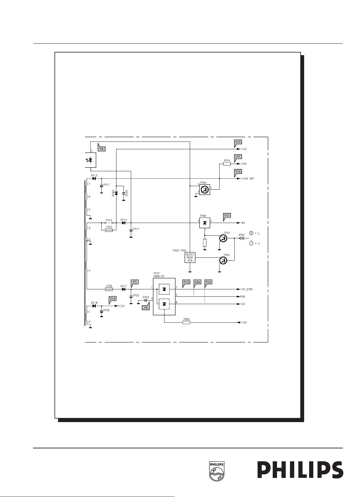
Output voltages
• +14V (For Line Circuit and input voltage for stabilizer 7908)
: +13.5V. If +14V and +8V are not present check 1905.
• +33V (For Tuner) : +33V. Created via R3994 and zenerdiode 6955
• Vbat (Battery Voltage for Line Output Stage) : +140V (9917
present) or +130V (9918 present).
• +8V (Bimos Supply ) : +8.3V. Output voltage from stabilizer
7908. This voltage is decreased in standby to 2V3. In standby TS7909 is conducting and switching R3933 parallel to
R3932. This will decrease the output voltage of 7908.
• +5Vstby (P Supply) : +5.1V. This voltage is also present
during standby. If this voltage and +5V are missing check
1906. If the voltage at pin 1 and 2 of IC7907 are present replace 7907.
• +5V (For Tuner, QSS, BTSC or ITT etc) : +5.1V. This voltage is disabled when the +13V is not present at pin 3 of
IC7907. +13V is generated by the line-output circuit. So
when the line-output circuit is working correctly the +5V is
enabled and the POR signal is generated to start the set.
• +15V ( Audio Supply) : +18V or +14V
Personal notes
A8.0A POWER SUPPLY 27
Control circuitry
Control circuitry
DEMAGNITIZING DETECTION CIRCUIT
6930
*
2
1N5062
2n2
9956
1R5
9952
9954
*
*
*
3902
3905
*
*
NTC
2904
41
2n2
2905
-t
1N5062
*
6933
6903
*
GBU4J
3
6932
*
1N5062
6931
*
3941
*
1N5062
(301V)
290V
2906
*
2M2
3917
*
10n
2920
*
17V6
(15V6)
7902
*
STR-F6626
4
VIN
1
OCFB2S
GND
1V6
(0V7)
P4
2915
470u
470p
100K
2912
5
3922
680R
P1
5912
*
TRANSFORMER
18
22n
3995
100K
2911
*
*
2971
6906
2913
5906
0R1
*
3n3
1n5
*
5911
*
6908
BYD33J
2966
*
3920
100P
3K3
P5
6911
BYD33J
BYD33M
P3
P2
47u
(301V)
290V
3
D
0V
(0V)
*
100mHz
3924
*
1
17
2
16
3
15
4
5
14
6
13
7
3959
*
3R3
6910
BYD33J
2K7
3962
*
1n5
1K5
3991
2914
*
*
12
8
11
9
10
CL 86532033_005.AI
030898
Mains input circuit
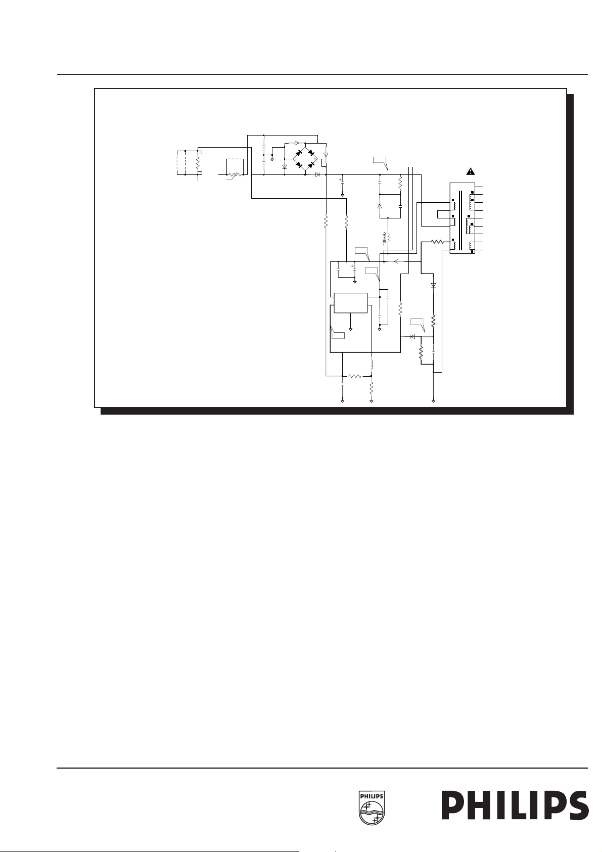
The mains voltage is rectified by bridge rectifier D6903 or
D6930 ,D6931 ,D6932, D6933 and filtered by C2906 . The DC
voltage across C2906 is the DC input voltage for the SMPS at
pin 6 of transformer T5912.
Start-up circuit
IC7902 is started when the voltage present at pin 4 is high
enough. When the set is switched on, C2912 is charged
through start-up resistor R3917. When the voltage across
C2912 reaches 16V (Typical), the control circuit of IC 7902
starts to operate.
After the control circuit starts itsoperation, power is supplied by
smoothing and rectifying the voltage of the supply winding ( 89 ) of T5912. The supply winding reaches the operation voltage
beforethe voltage of C2912 drops below theshutdown voltage.
Consequently, the control circuit can continue its operation.
Control circuit and oscillation phase
IC 7902 has two internal comparators . The thresholds of these
two comparators are 0.73V and 1.37V. During T-on , the MOSFET inside IC7902 is conducting . The voltage across R3924
increases due to the increase of the drain current. When the
voltage of pin 1 of IC7902 reaches the threshold voltage Vth(1)
=0.73V, the MOSFET turns off. The voltage of pin 8 of T5912
becomes now positive . Power supply flybacks at this moment
(so energy is released at the secondary side). Voltage applied
at pin1 of 7902 is determined by the turn ratio of the transformer T5912 and R3962, R3991 ( Typical voltage is 3.5V) . This
voltage is higher than threshold voltage Vth(2) (1.37V). Until
the transformer is demagnetized, this voltage remains high.
Once the energy stored in the transformer is fully transferred to
the secondary side, the voltage at pin1 of IC7902 drops below
the threshold voltage Vth1 after a certain delay time and a new
cycle starts.
 Loading...