

Page 1

Colour Television Chassis
A10PTV2.0
NTSC AA
Contents Page Contents Page
1. Technical Specifications, Connection Facilities
and Chassis Overview 2
2. Safety Instructions, Warnings and Notes 4
3. Directions For Use (Not Applicable) 5
4. Mechanical Instructions 5
5. Faultfinding and Repair Tips 7
6. Block Diagram, Wiring Diagram and Testpoints
Block Diagram 13
Testpoint Overview LSB Panel 14-15
Waveform Overviews 16
Testpoint Overview SSM Panel 17-18
Wiring Diagram 19
Supply Distribution Diagram 20
7. Electrical Diagram’s en PWB’s Diagram PWB
Large Signal Panel (Section 1) 21 24-29
Large Signal Panel (Section 2) 22 24-29
Large Signal Panel (Section 3) 23 24-29
CRT Red 30 33
CRT Blue 31 33
CRT Green 32 33
Small Signal Board (Section 1) 34 45-50
Small Signal Board (Section 2) 35 45-50
Small Signal Board (Section 3) 36 45-50
Small Signal Board (Section 4) 37 45-50
Small Signal Board (Section 5) 38 45-50
Small Signal Board (Section 6) 39 45-50
Small Signal Board (Section 7) 40 45-50
Small Signal Board (Section 8) 41 45-50
Small Signal Board (Section 9) 42 45-50
Small Signal Board (Section 10) 43 45-50
Small Signal Board (Section 11) 44 45-50
Side jack panel 51 52
Analog SSB:IF-Video-Sync-Chroma (Diagr. C1) 53 59-60
Analog SSB: Video Features (Diagram C2) 54 59-60
©
Copyright 2001 Philips Consumer Electronics B.V. Eindhoven, The Netherlands.
All rights reserved. No part of this publication may be reproduced, stored in a
retrieval system or transmitted, in any form or by any means, electronic, mechanical,
photocopying, or otherwise without the prior permission of Philips.
Analog SSB: Micro Controller (Diagram C3) 55 59-60
Analog SSB: Memory (Diagram C4) 56 59-60
Analog SSB: Audio Processing (Diagram C5) 57 59-60
Analog SSB: Audio Processing (Diagram C6) 58 59-60
Analog SSB: SSB Connector (Diagram C7) 59 59-60
Double Window: PIP (Diagram F1) 61 66-67
Double Window: Tuner (Diagram F2) 62 66-67
Double Window: I/O Processing (Diagram F3) 63 66-67
Double Window: IF-Video-Sync (Diagram F4) 64 66-67
Double Window: V-Chip Processor(Diagram F5) 65 66-67
Double Window: NV-ROM (Diagram F6) 65 66-67
PFC Filter Panel 68 69
SVM Panel 70 71
Center Channel Switch (Diagram K) 72 72
AC Power Switch (Diagram L) 73 73
Local Control 74 75
IR-LED (Keyboard) 76 77
8. Alignments 79
9. Circuit Description and 83
List of Abbreviations 99
10 Spare Parts List 101
Published by TA 0167 Service PaCE Printed in the Netherlands Subject to modification
3122 785 11241
Page 2
GB 2 A10PTV2.0 NTSC1.
Technical Specifications, Connections, and Chassis Overview
1. Technical Specifications, Connections, and Chassis Overview
1.1 Technical Specifications
Mains Voltage : 90 V - 276 V
Power Consumption : 260 W max
Standby consumption : < 3 W
Mains Frequency : 50 / 60 Hz (+/- 5%)
Tuning System : PLL
Reception : NTSC M,
Sound System : BTSC DBX - / 97
Sound Output : 2 x 15W
(+/- 10%)
(3.58 - 4.5)
:FM / FM
(4.5 - 4.72) - / 61
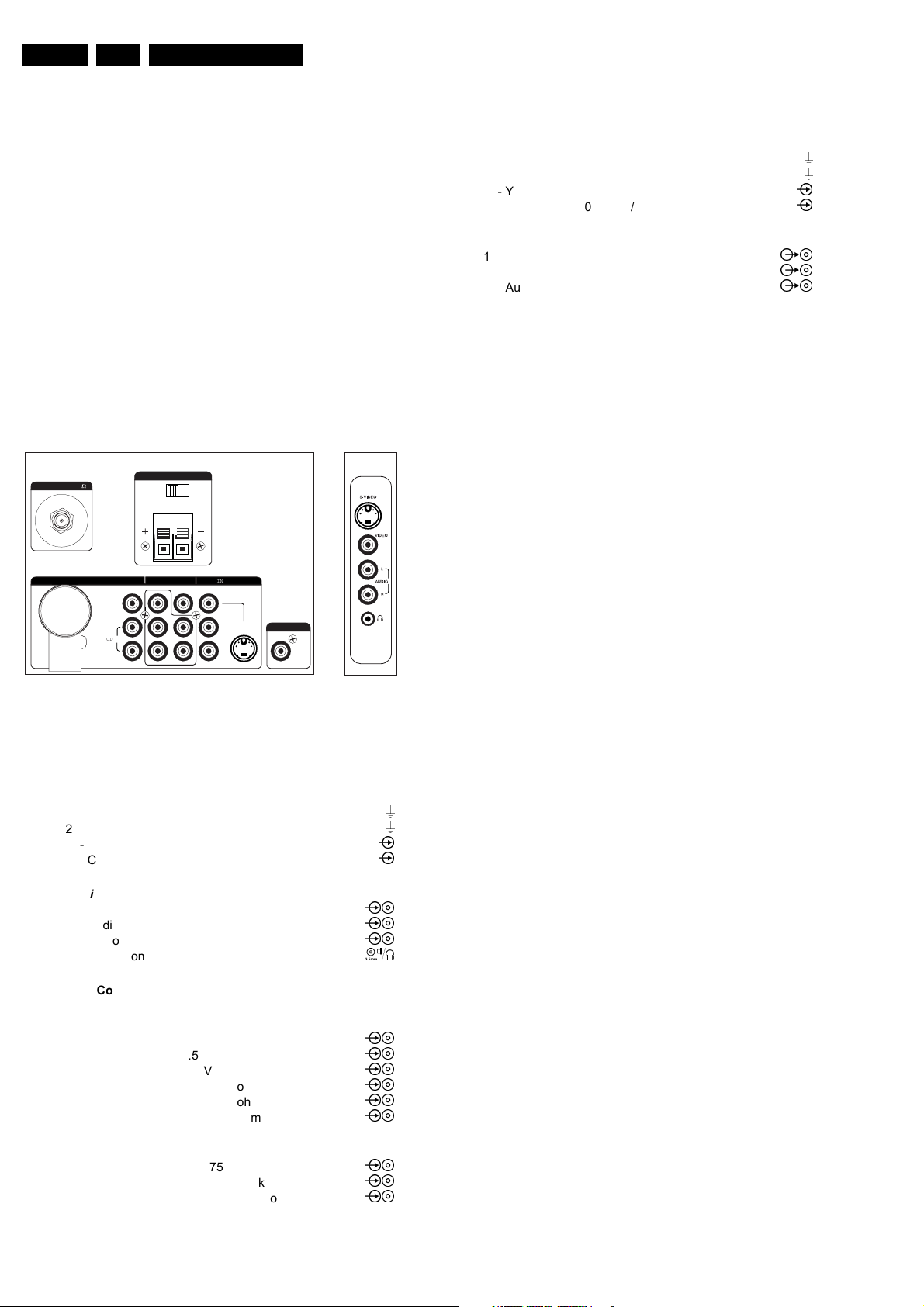
1.2 Connection Diagram
Audio/Video Jack Panels
Rear
ANTENNA IN 75
MONO/L
VIDEO
AUDIO
CENTER CHANNEL AMP INPUT
R
AMP SWITCH
EXT
Y
Pb
Pr
INT
AV2 INAV1 INMONITOR OUT
S-VIDEO
SUBWOOFER
V
Side
CL 06532143_001.eps
011100
AV2 In (SVHS)
1 - gnd
2 - gnd
3 - Y 1 Vpp / 75 ohm
4 - C 0.3 Vpp / 75 ohm
Monitor Out
1 - Video 1 Vpp / 75 ohm
2 - Audio L (0.5 Vrms / 10 k ohm)
3 - Audio R (0.5 Vrms / 10 k ohm)
Figure 1-1
1.2.1 Side Connections
SVHS
1 - gnd
2 - gnd
3 - Y 1 Vpp / 75 ohm
4 - C 0.3 Vpp / 75 ohm
Audio / Video
1 - Video 1 Vpp / 75 ohm
2 - Audio Left (0.2 Vrms / 10 k ohm)
3 - Audio Right (0.2 Vrms / 10 k ohm)
4 - Headphone 32 - 2000 ohm / 10 mW
1.2.2 Rear Connections
AV1 In
1 - Video 1 Vpp / 75 ohm
2 - Audio L (0.5 Vrms / 10 k ohm)
3 - Audio R (0.5 Vrms / 10 k ohm)
4 - Y 0.7 Vpp / 75 ohm
5 - Pb 0.7 Vpp / 75 ohm
6 - Pr 0.7 Vpp / 75 ohm
AV2 In
1 - Video 1 Vpp / 75 ohm
2 - Audio L (0.5 Vrms / 10 k ohm)
3 - Audio R (0.5 Vrms / 10 k ohm)
Page 3
Technical Specifications, Connections, and Chassis Overview
Side J
Blue CR
C P
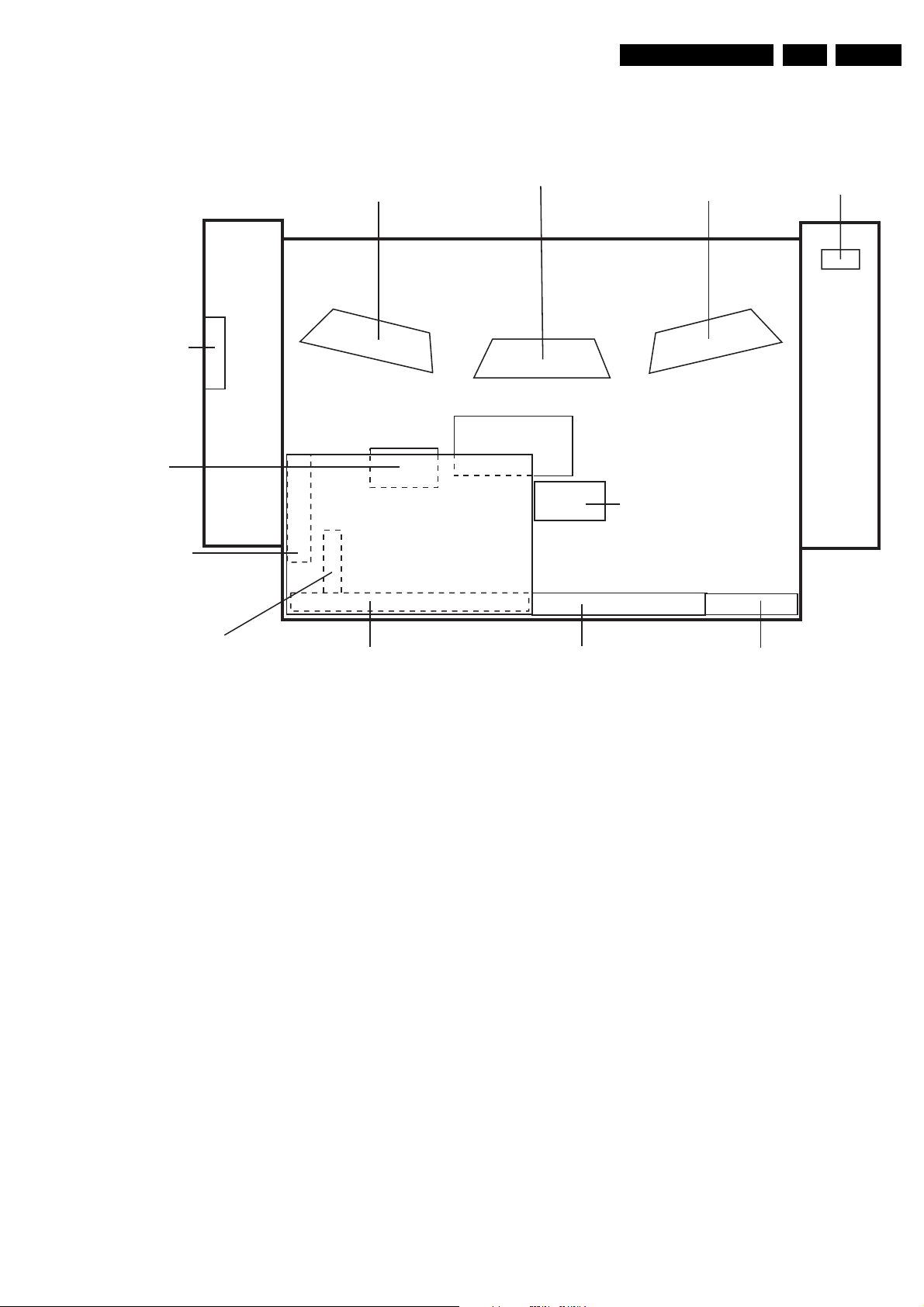
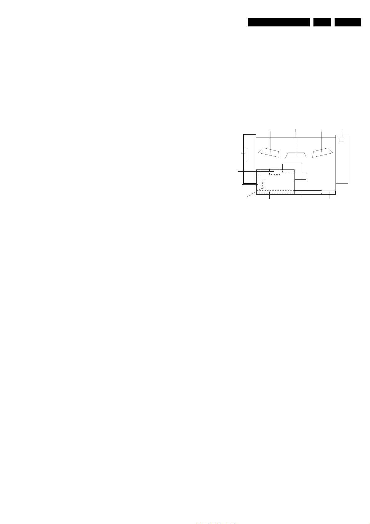
1.3 Chassis Overview
ack
Side J
Panel
Center
Channel
Switch
Red CRT
Green CRT
SVM Panel
Blue CR
Keyboard &
IR LED Panel
GB 3A10PTV2.0 NTSC 1.
AC P
ower
T
Switch Panel
PIP Panel
SSB Module
SSM Panel
LSB Panel
Figure 1-2
Filter Panel
CL 16532050_001.eps
090501
Page 4

GB 4 A10PTV2.0 NTSC2.
Safety Instructions, Warnings and Notes
2. Safety Instructions, Warnings and Notes
2.1 Safety Instructions for Repairs
• Safety regulations require that during a repair:
– The set should be connected to the mains via an
isolating transformer;
– Safety components, indicated by the symbol
should be replaced by components identical to the
original ones;
– When replacing the CRT, safety goggles must be
worn.
• Safety regulations require that after a repair the set must
be returned in its original condition. In particular attention
should be paid to the following points.
– General repair instruction: As a strict precaution, we
advise you to resolder the solder joints through which
the horizontal deflection current is flowing, in
particular
a. All pins of the line output transformer (LOT);
b. Fly-back capacitor(s);
c. S-correction capacitor(s);
d. Line output transistor;
e. Pins of the connector with wires to the deflection
coil;
f. Other components through which the deflection
current flows.
Note: This resoldering is advised to prevent bad
connections due to metal fatigue in solder joints
and is therefore only necessary for television
sets older than 2 years.
– The wire trees and EHT cable should be routed
correctly and fixed with the mounted cable clamps.
– The insulation of the mains lead should be checked
for external damage.
– The mains lead strain relief should be checked for its
function in order to avoid touching the CRT, hot
components or heat sinks.
– The electrical DC resistance between the mains plug
and the secondary side should be checked (only for
sets which have a mains isolated power supply). This
check can be done as follows:
1. Unplug the mains cord and connect a wire
between the two pins of the mains plug;
2. Set the mains switch to the "on" position (keep
the mains cord unplugged!);
3. Measure the resistance value between the pins
of the mains plug and the metal shielding of the
tuner or the aerial connection on the set. The
reading should be between 4.5 M9 and 12 M9
4. Switch off the TV and remove the wire between
the two pins of the mains plug.
– The cabinet should be checked for defects to avoid
touching of any inner parts by the customer.
2.2 Maintenance Instruction
It is recommended to have a maintenance inspection carried
out by a qualified service employee. The interval depends on
the usage conditions:
,
• When the set is used under normal circumstances, for
example in a living room, the recommended interval is 3
to 5 years.
• When the set is used in circumstances with higher dust,
grease or moisture levels, for example in a kitchen, the
recommended interval is 1 year.
• The maintenance inspection contains the following
actions:
– Execute the above mentioned 'general repair
instruction'.
– Clean the power supply and deflection circuitry on
the chassis.
– Clean the picture tube panel and the neck of the
picture tube.
2.3 Warnings
•ESD
• Available ESD protection equipment:
• Be careful during measurements in the high-voltage
• Never replace modules or other components while the
• When making settings, use plastic rather than metal
All ICs and many other semiconductors are susceptible
to electrostatic discharges (ESD). Careless handling
during repair can reduce life drastically. When repairing,
make sure that you are connected with the same
potential as the mass of the set by a wristband with
resistance. Keep components and tools also at this same
potential.
– Complete kit ESD3 (small table mat, Wristband,
Connection box, Extension cable and Earth cable)
4822 310 10671
– Wristband tester 4822 344 13999
section and on the picture tubes.
unit is switched on.
tools. This will prevent any short circuits and the danger
of a circuit becoming unstable.
2.4 Notes
• The direct voltages and oscillograms should be
measured with regard to the tuner earth (
) as this is called.
(
• The direct voltages and oscillograms shown in the
diagrams are indicative and should be measured in the
Service Default Mode (see chapter 5) with a colour bar
signal and stereo sound (L: 3 kHz, R: 1 kHz unless stated
otherwise) and picture carrier at 475.25 MHz.
• Where necessary, the oscillograms and direct voltages
are measured with (
Voltages in the power supply section are measured both
for normal operation (
values are indicated by means of the appropriate
symbols.
• The picture tubes PWB have printed spark gaps. Each
spark gap is connected between an electrode of the
picture tube and the Aquadag coating.
• The semiconductors indicated in the circuit diagram and
in the parts lists are completely interchangeable per
position with the semiconductors in the unit, irrespective
of the type indication on these semiconductors.
) and without aerial signal ().
) and in standby (). These
), or hot earth
Page 5
3. Directions for Use
PHILIPS
4. Mechanical Instructions
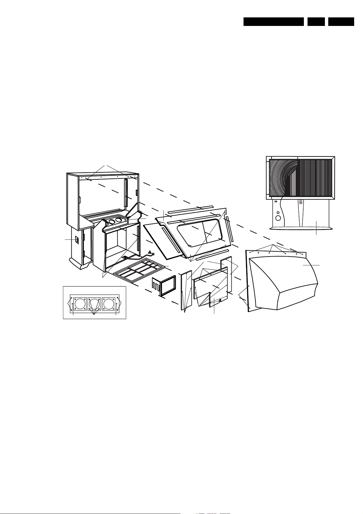
4.1 Disassembly Procedures
All numbers found in the following text refer to the
CABINET DISASSEMBLY EXPLODED VIEW drawing and
apply to all models.
NOTE: If you are only servicing a PCB or speaker, you do not
have to remove the plastic upper back cover.
CABINET DISASSEMBLY EXPLODED VIEW
J
Directions for Use
GB 5A10PTV2.0 NTSC 3.
PHILIPS
16
22
!
27
Optical Assembly
GG
E
H
E
4.1.1 Removal of Upper Back Cover (2)
1. Remove 8 screws (A).
2. Remove 3 screws (B).
3. Lift cover up to dislodge from pegs (J) and remove cover.
4.1.2 Removal of Lower Center Back Cover (1)
1. Remove 3 screws (B).
2. Remove 8 screws (C).
4.1.3 Removal of Mirror Mounting Board (18)
1. Remove 6 screws (D) located in the mirror mounting
board and remove the board.
NOTE: Care should be taken NOT to place fingerprints or
smudges on mirror.
4.1.4 Removal of Plastic Light Barrier (16)
1. Remove two screws (E) located at the sides of the Plastic
Light Barrier.
18
A
Right
3
Left
D
B
C
F
1
6
F
A
30
2
CL 06532143_003.eps
011100
Figure 4-1
4.1.5 Removal of Side Back Covers (3)
NOTE: To gain access to the Side Jack Panel (D) and two
Speakers, remove the Left Side Back Cover.
To gain access to the AC Power Switch Panel (L), remove
the Right Side Back Cover.
1. Remove 4 screws (F) from each of the Side Back Covers.
4.1.6 Removal of Large Signal Panel (A)
1. Pull 3 tabs on right of bracket and 2 tabs on left of
bracket.
2. Lift Large Signal Board up and out.
4.1.7 Removal of PFC Filter Panel (G)
1. Remove 4 screws from CBA.
2. Lift PFC Filter Panel up and out.
4.1.8 Removal of Small Signal Panel (C)
1. Remove 2 screws from the middle of the CBA.
2. Pull 3 tabs on right of bracket.
Page 6

GB 6 A10PTV2.0 NTSC4.
3. Lift Small Signal Board up, then to the right to remove.
4.1.9 Removal of Side Jack Panel (22) (D)
1. Remove Left Side Back Cover.
2. Pull tabs in; press Side Jack Panel out.
3. Remove two screws from panel.
4. Slide Side Jack Panel CBA out of bracket.
4.1.10 Removal of AC Power Switch Panel (L)
1. Remove Front Baffle (30) by gently pulling baffle frame
away from cabinet.
2. Remove Right Side Back Cover.
3. Remove 2 screws from panel.
4. Remove 2 plugs 1000 & 1002.
5. Pull panel out front of set.
4.1.11 Removal of Center Channel Switch Panel (K)
1. Remove 3 screws from panel.
4.1.12 Removal of Double Window PIP Panel (F)
1. Remove 3 screws from panel.
Mechanical Instructions
4.1.13 Removal of Analog SSB (E)
1. Pull frame up.
2. Pull board to right and then up.
4.1.14 Removal of Front Control
1. Remove front speaker baffle (30) by gently pulling baffle
frame away from cabinet.
2. Remove 3 screws from front control.
4.1.15 Removal of Euro SVM Panel (J)
1. Press 3 treelocks to remove Euro SVM board.
4.1.16 Removal of Complete Optical Assembly or Individual
Light Box Assemblies.
1. Remove the Plastic Light Barrier (16).
2. Separate CRT CBA's from assemblies to be removed.
3. To remove the complete Optical Assembly, loosen 4
screws (G) located in the assembly, and lift assembly up
and out.
4. To remove individual Light Box assemblies, loosen 4
screws (H) located in the assembly you wish to remove
and lift assembly up and out.
Page 7
Fault Finding and Repair Tips
5. Fault Finding and Repair Tips
GB 7A10PTV2.0 NTSC 5.
The lowing topics are covered:
• Test points
• Service Modes
• Error code buffer and error codes
• The “blinking LED” procedure
• Trouble shooting tips
• Customer Service Mode
5.1 Test Points
The A10 PTV chassis is equipped with test points shown on
the schematic diagrams.
Each test point has a reference number indicating the
schematic diagram on which it is located.
• A F106, A I126, etc.: Test points for the Large Signal
Panel [A1 - A3]
• C F001, C I001, etc.: Test points for the Small Signal
Panel [C1 - C11]
• G F114, G I001, etc.: Test points for the PFC Filter Panel
[G]
• J F004, J F006, etc: Testpoints for the SVM Panel [J]
• K I001, K I002: Test points for the Center Channel Switch
[K]
• M I004, M I005: Test points for the Local Control [M]
Measurements should be performed under the following
conditions:
Video: color bar signal
Audio: 3kHz left, 1kHz right
Note:The measurements at the following test points were
taken using a 100:1 probe:
• A I142
• A I220
5.2 Service Default Mode (SDM)
5.2.1 Introduction
The Service Default Mode (SDM) is a technical aid for the
service technician. The Service Default Mode (SDM)
establishes fixed, repeatable settings of customer controls,
which allow consistent measurements to be made. The SDM
also initiates the blinking LED procedure and, if necessary,
overrides the 5V protection. This mode also allows the
operating hours, the software version and error codes to be
read.
5.2.2 Entering Service Default Mode
To enter the Service Default Mode, press the following key
sequence on the remote control transmitter:
0-6-2-5-9-6-MENU
Do not allow the display to time out between entries while
keying the sequence.
Upon entry into the Service Default Mode, the letters “SDM”
will be displayed at the upper right corner of the screen.
Side Jack
Panel
Center
Channel
Switch
PIP Panel
SSB Module
Red CRT
SSM Panel
Green CRT
SVM Panel
LSB Panel
Blue CRT
Keyboard &
IR LED Panel
Figure 5-1
5.2.3 Special SDM Functions
Access to Normal User Menu
Pressing the “MENU” button on the remote control switches
between the SDM and the normal user menus (with the SDM
mode still active in the background)
Run Timer, Software Identification, and Error Buffer
Press the Index or status button on the remote control to
toggle the OSD (except “SDM”) ON and OFF to prevent the
OSD from interfering with measurements and oscilloscope
waveforms.
Access to SAM
To access the Service Alignment Mode while in the SDM
press the “VOLUME +” and “VOLUME -“ buttons on the local
keyboard simultaneously for at least 4 seconds.
5.2.4 Exiting Service Default Mode
Filter Panel
CL 16532050_001.eps
AC Power
Switch Panel
090501
The SDM Places the Set in the Following Pre-defined
Conditions:
• Tuning frequency set to channel 3.
• Volume level set to 25% (of the maximum volume level).
• Other picture and sound settings set to 50% (mid-range).
The Following Functions are Turned Off in SDM (and
After Leaving SDM):
•Timer
• Sleep timer
The Following Functions are Disabled During SDM (and
Enabled After Leaving SDM):
• Parental lock
All other controls operate normally.
To exit the Service Default Mode, press the Power button.
Page 8

GB 8 A10PTV2.0 NTSC5.
Fault Finding and Repair Tips
5.3 Service Alignment Mode (SAM)
5.3.1 Introduction
The Service Alignment Mode (SAM) is used to align the set
and/or adjust the option settings and to display/clear the error
code buffer values.
Entering Service Alignment Mode
To enter the Service Alignment Mode (SAM), press the
following key sequence on the remote control transmitter:
0-6-2-5-9-6-INDEX or status.
Do not allow the display to time out between entries while
keying the sequence
It is also possible to enter the Service Alignment Mode by
pressing the “VOLUME +” and “VOLUME -” key on the local
keyboard simultaneously for at least 4 seconds when the set
is in SDM.
5.3.2 Exit SAM:
To exit the Service Alignment Mode, press the Power button.
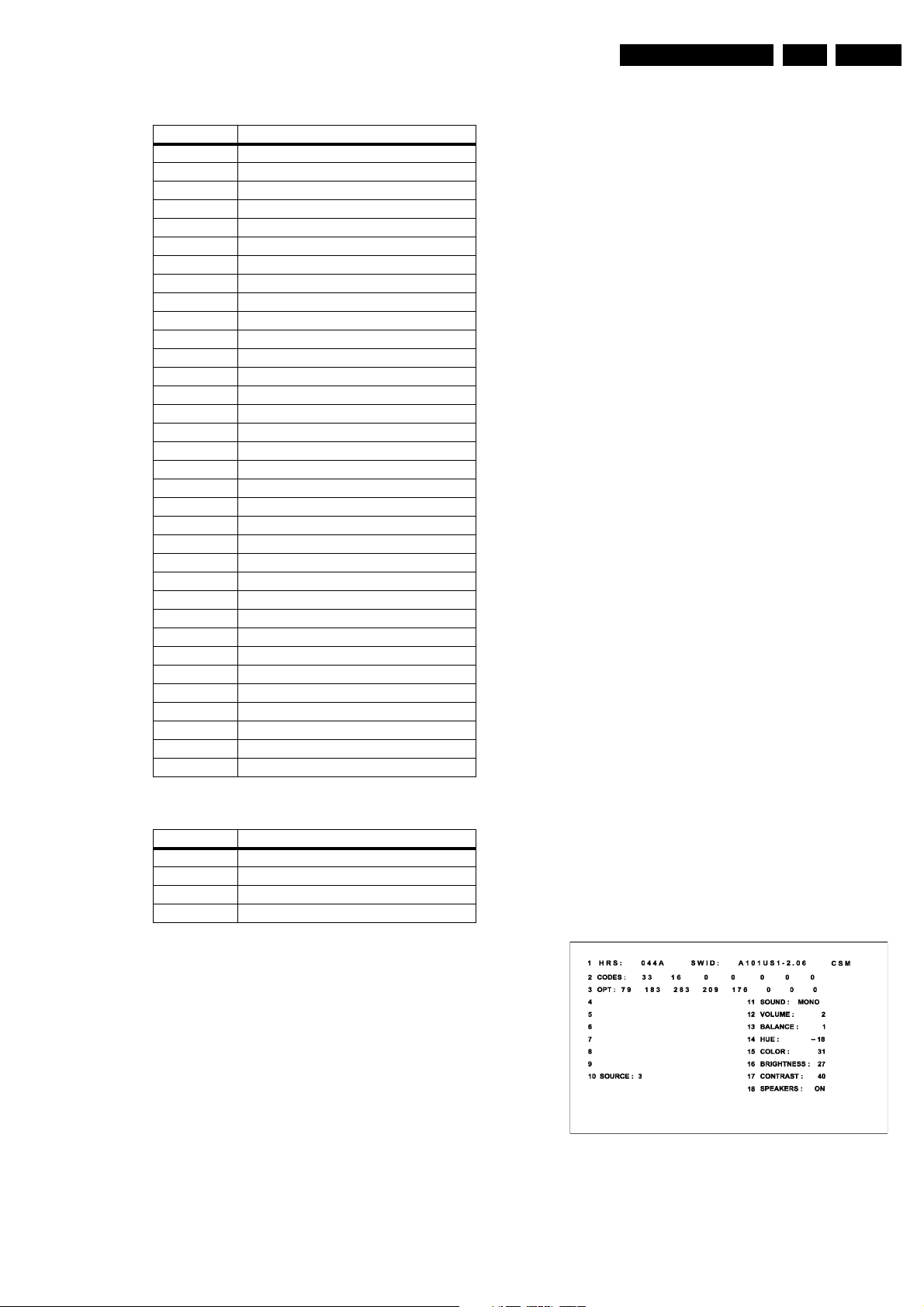
In SAM the following information is displayed on the screen:
Figure 5-2
5.3.3 Explanation Notes/References:
1. Operation Hours (Run Timer):
• This display indicates the accumulated total of
operational hours. (Shown in hexadecimal format)
2. Software identification of the main micro controller
(A101US1-2.06)
• A10 is the engineering chassis name for the A10
PTV chassis
• 1US1 is a character combination to indicate the
software type and the supported languages: 3AP1 or
3AP2 are also possible in the Asian Pacific Region.
• US = United States, AP = Asia Pacific
• 1 = Main Software language version number
• 2.06 = sub-version number
3. Error buffer (7 errors possible):
• Displays the 7 most recent errors. The most recent
error is displayed at the upper left.
4. Option bytes (8 codes possible):
• Summary of options is explained below.
5. Sub menus are listed in a scroll menu.
5.3.4 SAM Menu Control
Menu items may be selected using the cursor UP/DOWN
keys.
• The selected item will be highlighted.
• When not all menu items will fit on the screen, pressing
the cursor UP/DOWN keys on the remote transmitter will
display the next/previous menu items.
CL 16532052_003.eps
090501
With the cursor LEFT/RIGHT keys, it is possible to:
• (de)activate the selected menu item (e.g. GEOMETRY)
• change the value of the selected menu item ( e.g. VERSLOPE )
• activate the selected submenu (e.g. SERV-BLK)
Access to Normal User Menu
Pressing the “MENU” button on the remote control switches
between the SAM and the normal user menus (with the SAM
mode still active in the background). Pressing the “MENU”
key in a submenu will return the screen to the previous menu.
5.4 The Menus and Submenus
5.4.1 Clear Errors
Erases the contents of the error buffer. Select the CLEAR
ERRORS menu item and press the cursor LEFT or cursor
RIGHT key. The contents of the error buffer are cleared.
The functionality of the OPTIONS and ALIGNMENTS
(TUNER, WHITE TONE, GEOMETRY, SOUND, and
SMART SETTING) submenus are described in the service
adjustments.
5.4.2 Error Code Buffer and Error Codes
Explanation of the Error Code Buffer
The error code buffer contains all errors detected since the
last time the buffer was erased. The buffer is written from left
to right. When an error occurs that is not yet in the error code
buffer, the error code will appear at the left side and all other
errors shift one position to the right.
The error code buffer will be cleared in the following cases:
• by activating CLEAR ERRORS in SAM menu
• exiting SDM or SAM with the “Standby" command on the
remote control
• upon automatic reset when content has not changed for
50 consecutive hours
By leaving SDM or SAM via the power switch, the error buffer
will not be reset.
Examples:
ERROR: 0 0 0 0 0 0 0 :No errors detected
ERROR: 6 0 0 0 0 0 0 :Error code 6 is the last and only
detected error
ERROR: 9 6 0 0 0 0 0 :Error code 6 was first detected and
error code 9 is the last detected (newest) error
The contents of the error buffer can also be displayed by use
of the “blinking LED” procedure, if no picture is available. See
explanation of “The blinking LED procedure “below.
5.4.3 Error Code Definition
In case of non-intermittent faults, clear the error buffer before
starting the repair, to make sure “old” error codes are not
present. If possible check the entire content of the error
buffers. In some situations an error code is only the result of
another error code (and not the actual cause).
Note: a fault in the protection detection circuitry can also lead
to a protection.
Error codes 1,2, 3, and 4 are protection codes, and in this
case the supplies of some circuits will be switched off. Also
in protection, the LED will blink the number of times
equivalent to the most recent error code.
Page 9
Fault Finding and Repair Tips
GB 9A10PTV2.0 NTSC 5.
5.4.4 Error Code Table
Code Number Error Description
00 Not an Error
01 Too high I-beam or East/West protection
02 Vertical protection
03 X-Ray protection
04 5 volt protection
05 - not used
06 General IIC error
07 BC loop not stabilised
08 Bocma TDA888X IIC error
09 Bocma IC 8v failure
10 NVM IIC communication error
11 Wrong NVM type
12 Microp internal RAM error
13 Main tuner IIC failure
14 Sound IC failure
15 SRAM test failure
16 PIP Tuner IIC failure
17 ECO Pip IC or DW Pip IC failure
18 I/O expander I2C error
19 Gemstar Guide Plus board
20 V-chip located on the DW Pip
21 Non-Volatile clock
22 Incredible picture (YUV) CR
23 Bocma DoubleWindow TDA888X error
24 - not used
25 - not used
26 - not used
27 Virtual Dolby
28 - not used
29 - not used
30 CSP i2c error
31 CSP NVM i2c error
32 CSP NVM error - not valid data
33 CSP dac i2c error
5.4.5 A10 PTV Model Listing & Software
Model Software
43PP925/61 3AP2
43PP925/97 3AP1
55PP925/61 3AP2
55PP925/97 3AP1
Error buffer: 12 9 6 0 0
• After entering SDM:
• The sequence will begin with 1 long blink of 750
mSeconds, then pause 1500 mSeconds, then blink twice
(indicating error code 12), then the LED will pause for 3
seconds, then blink 9 times (indicating error code 9), then
the LED will pause for 3 seconds, then blink 6 times
(indicating error code 6), then pause 3 seconds and blink
for 3 seconds again, ending the blinking sequence.
NOTE: If errors 1, 2, 3, or 4 occur the LED ALWAYS
blinks indicating the last error which occurred, even if
the set is NOT in service mode.
5.6 Customer Service Mode
All A10 PTV sets are equipped with the “Customer Service
Mode” (CSM). CSM is a special service mode that can be
activated and deactivated by the customer, by request of the
service technician/dealer in order to identify the status of the
set. This CSM is a 'read only' mode, therefore modifications
in this mode are not possible.
5.6.1 Entering the Customer Service Mode.
The Customer Service Mode can be switched on:
• By pressing the MUTE button on the remote control and
any key on the local keyboard (Channel Up, Channel
Down, VOL +, VOL -) on the TV simultaneously for at
least 4 seconds.
When the CSM is activated:
• picture and sound settings are set to nominal levels
• Modes that interfere with the behavior of the set are
switched off (sleep timer, auto standby, etc.)
5.6.2 Exit the Customer Service Mode.
The Customer Service Mode will be switched off after:
• Pressing any key on the remote control (except “Channel
Up” or “Channel Down”)
• Switching off the TV set by pressing the Power button on
the remote control or the local keyboard.
Exiting CSM resets the TV set back to its initial values.
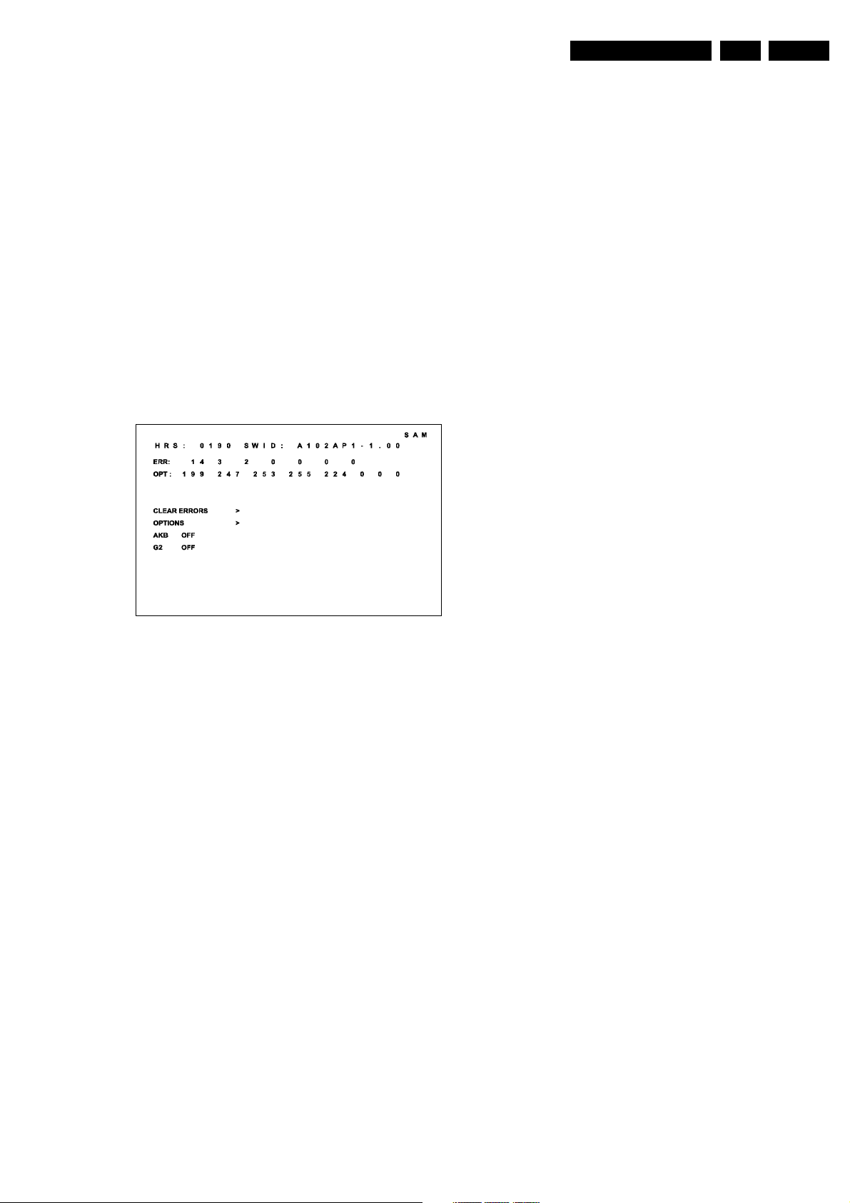
5.6.3 The Customer Service Mode information screen
Upon entry into the Customer Service Mode the following
screen will appear.
5.5 The Blinking LED Procedure
The contents of the error buffer can also be made visible
through the “blinking LED” procedure. This is especially
useful when there is no picture.
• When the SDM is entered, the LED will blink the number
of times equal to the value of the error code. Upon entry
into the SDM, the LED will blink the contents of the errorbuffer. Error-codes greater than/equal to 10 are shown in
the following manner: A long blink of 750 mSeconds
indicating the decimal digit, followed by a pause of 1500
mSeconds. The LED will then blink the number equal to
the error code. When all error-codes are displayed, the
sequence is finished with an LED display of 3 seconds.
At this point the sequence will begin again.
Example:
Error code position 1 2 3 4 5
CL 16532052_002.eps
Figure 5-3
The Customer Service Menu shows the following
information:
090501
Page 10

GB 10 A10PTV2.0 NTSC5.
Fault Finding and Repair Tips
Line 1 : “HRS : nnnnn” and SWID : “A102BBC-X.YY”
HRS:
Indicates the accumulated total of operational hours. (Shown
in hexadecimal format.) (Standby hours are not counted as
operating hours).
SWID:
Software identification of the main micro controller (A10US1-
2.7)
A10 is the chassis name for the A10 PTV
• 1US1 is a character combination to indicate the software
type and the supported languages: 3AP1 or 3AP2 are
also possible for the Asian Pacific Region.
• US = USA/NAFTA, AP = Asia Pacific region
• 1 = Main Software language version number
• 2.7 = sub-version number
Line 2 : “CODES : xx xx xx xx xx xx xx ”
Error code buffer (see explanation of error codes above)
Displays the last 7 errors of the error code buffer.
Line 3 : “OPT xxx xxx xxx xxx xxx xxx xxx xxx”
Option bytes
Option bits control the software and hardware functionality of
the A10.0. An option byte or option number represents 8 of
those bits. Each option number is displayed as a number
between 0 and 255. The set may not work correctly when an
incorrect option code is set. See Service Adjustments for
more information on correct option settings
4. Set to “ADD” with the left/right cursor keys
Line 9 : “HOTELMODE ON”
Indicates that the Hotel mode has been activated.
Line 10 : “SOURCE :”
Indicates which SOURCE is installed for this preset.
EXT1, SVHS2, EXT2, Tuner
Line 11 : “SOUND”
Indicates which sound mode is installed for this preset.
Mono, NICAM, Stereo, L1, L2, SAP, Virtual or Digital
Line 12 : “VOLUME”
Value indicates level at CSM entry.
Line 13 : “BALANCE”
Value indicates level at CSM entry.
Line 14 : “HUE”
Value indicates level at CSM entry.
Line 15 : “COLOUR”
Value indicates level at CSM entry.
Line 16 : “BRIGHTNESS”
Value indicates level at CSM entry.
Line 17 : “CONTRAST”
Value indicates level at CSM entry.
Line 4: NOT USED
Line 5 : “NO SIGNAL”
Indicates that the set is not receiving an “ident” signal on the
selected source.
• no or bad antenna signal; connect a proper antenna
signal
• antenna not connected; connect the antenna
• no channel / preset is stored at this program number; go
to the INSTALL menu and store a proper channel at this
program number
• the tuner is faulty (in this case the CODES line will
contain number 13 or 16); check the tuner and replace/
repair if necessary
Note: On some models (if the BM option is ON), BLUE
MUTE is displayed when no signal is received.
Line 6 : “TIMER ON ”
Indicates that the on/off timer is running.
The following Complaints may be caused by the activation of
the sleep timer:
The set may turn on from standby or may switch to a different
channel without using either the remote control or the local
keyboard.
To switch off the activation timer:
Select “TIMER” in the “FEATURE” menu.
Select “ACTIVATE” in the “TIMER” menu.
Set to “OFF” with the left/right cursor keys.
Line 7 : NOT AVAILABLE
Line 8 : “NOT PREFERED”
Indicates that at least one channel is deleted as a preferred
channel (by default, all channels are skipped).
Note that “SKIPPED” will always be displayed in CSM
unless all the channels are not skipped.
To add a channel as a selected channel to the list of preferred
channels:
1. Select “INSTALL” menu
2. Select “CHANNEL EDIT”
3. Select “ADD/DELETE”
Line 18: “SPEAKERS”
Indicates the speakers are “ON” or “OFF”.
Page 11
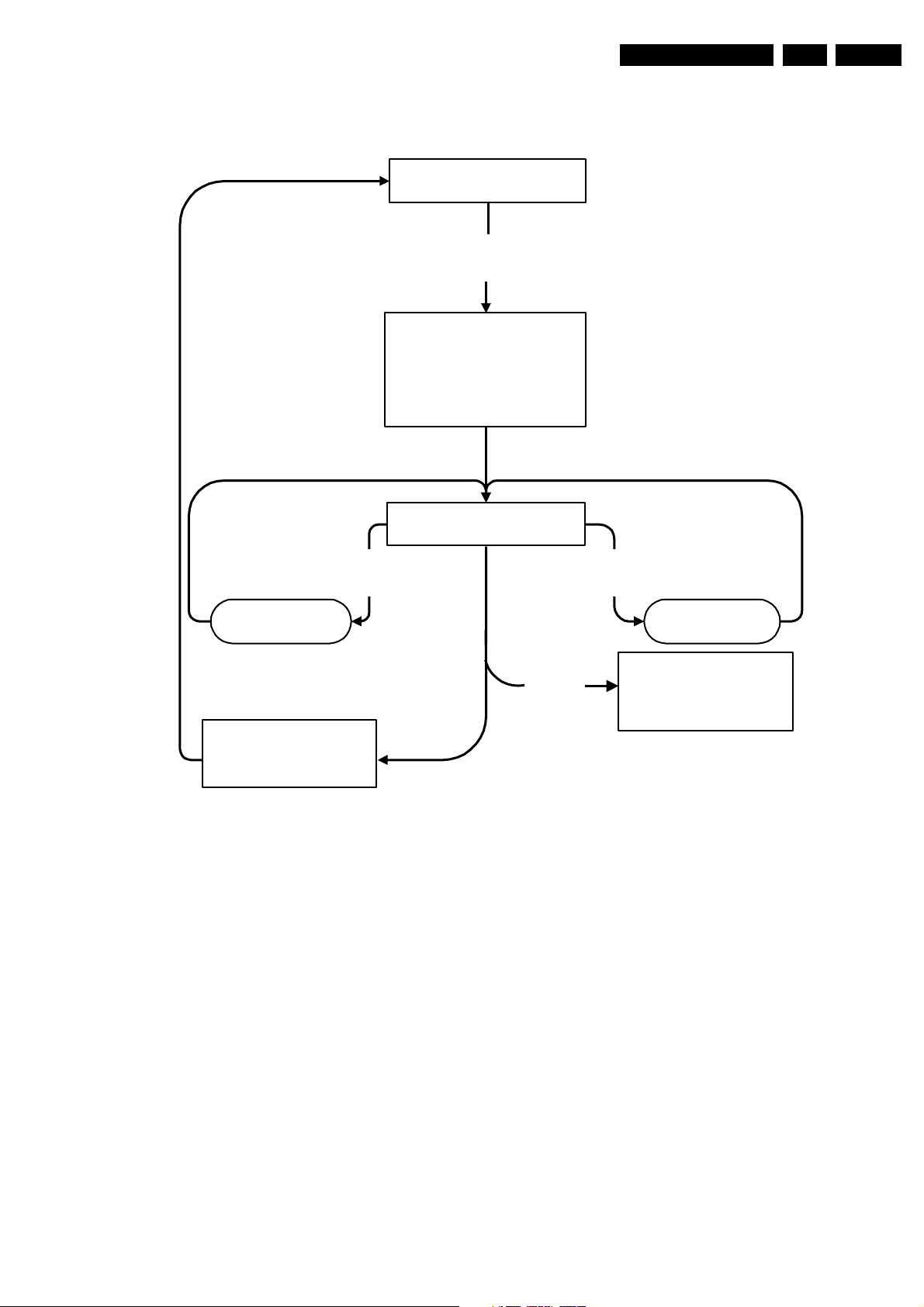
5.6.4 CSM Flow Chart
y
p
Fault Finding and Repair Tips
Normal operation mode
Press "MUTE" button (RC) and
key on the local keyboard
an
(except "POWER") for more than 4 seconds
Store current picture, sound and
feature settings (for later retrieval)
Set pre-defined picture, sound and
feature settings
Ignore service unfriendly options
GB 11A10PTV2.0 NTSC 5.
"Channel up"
(RC or local
keyboard)
Exit CSM
Restore picture, sound and
a
n
a
stored during entry)
Display CSM information screen
POWER
(RC or local
Other key
Figure 5-4
keyboard)
"Channel down"
(RC or local
keyboard)
Off (Exit CSM):
when the set is switched on,
icture, sound and feature
settings (that were stored
during entry) are restored
To next CSM pageTo previous CSM page
CL 06532143_007.eps
011100
Page 12

GB 12 A10PTV2.0 NTSC5.
Fault Finding and Repair Tips
5.7 Trouble Shooting Tips
5.7.1 The Power Supply Circuit:
When the set is turned On,the Main Switch Mode power
supply is turned On This supply produces the +130 volt,+32
volt,-32 volt,two +15 volt,and Audio supplies. When IC 7302
develops a normal steady state operation,the 130 volt supply
is sampled by resistors 3324,3323,and 3322.
This sample voltage is then sent to Shunt regulator 7303
which drives the feedback optoisolator 7303.The feedback
voltage on Pin 14 is then compared with an internal 2.5 volt
reference by comparator "C". Comparator "C"then sets the
reference voltage on the inverting side of comparator "B"to
control the On time of the drive at Pin 3.If the voltage on Pin
14 increases due to the 130 volt supply increasing,the On
time of the pulse on Pin 3 will be reduced.If the 130 volt
supply decreases,the voltage on Pin 14 would
decrease,causing the On time of the pulse on Pin 3 to
increase.This is used to keep the 130 volt supply at the
correct voltage.Variable resistor 3322 is used to adjust the
130 volt supply to the correct level.
The overvoltage protection circuit of the IC will shut the IC
down if the VCC level on Pin 1 exceeds 17 volts.
To troubleshoot this circuit,first check the On/Off line from the
Small Signal Panel to ensure that it is going Low.Then check
for the presence of startup voltage on Pin 1 of the regulator
IC 7302.If the IC is working correctly,this voltage will be
changing from 9.4 to 14.5 volts.If the startup voltage is not
present,check the startup resistor 3300 and the bridge
rectifier.If the voltage on Pin 1 is changing,check the drive
signal on Pin3.Then check for signal on the gate and drain of
7301.An excessive load on the secondary,a short on the 130
volt line for example,would cause the supply to pulse with
little or no voltage on the secondary.
Sound Problems
No sound or sound too loud (after channel change / switching
on)
– Enter the Customer Service Mode. If the volume is OK,
increase / decrease the volume level.
5.7.2 Picture Problems
Picture Too Dark or Too Bright
– Press “Smart Picture” button on the remote control. If this
improves the picture, increase / decrease the brightness
value or increase / decrease the contrast value.
– Enter the Customer Service Mode. If this improves the
picture, exit Customer Service Mode, then Increase /
decrease the brightness value or increase / decrease the
contrast value.
White Line Around Picture Elements and Text
– Press “Smart Picture” button on the remote control. If this
improves the picture, decrease the sharpness value.
– Enter the Customer Service Mode. If this improves the
picture. Decrease the sharpness value.
Snowy Picture
– Snow is an antenna or antenna connector problem.
Check tuner and AGC.
Black and White Picture
– Press the “Smart Picture” button on the remote control. If
this improves the picture, increase the color value.
– Enter the Customer Service Mode. If this improves the
picture. Increase the color value.
Menu Text Not Sharp Enough
– Press the “Smart Picture” button on the remote control. If
this improves the picture, decrease the contrast value.
– Enter the Customer Service Mode. If this improves the
picture. Decrease the contrast value.
Page 13
8. Alignments
Alignments
GB 79A10PTV2.0 NTSC 8.
General: The Service Default Mode (SDM) and Service
Alignment Mode (SAM) are described in Chapter 5.
8.1 Alignment Conditions
All electrical adjustments should be performed under the
following conditions:
• Supply voltage : 120V +/- ( 10%)
• Warm-up time: 10 minutes
• The voltages and oscilloscope waveforms are measured
in relation to the tuner ground.
• Test probe: Ri > 10Meg Ohm; Ci < 2.5 pF.
8.2 Software Alignments (Service Alignment
Mode)
With the software alignments of the Service Alignment Mode,
the geometry, white tone and tuner (IF) can be aligned.
CL 16532052_003.eps
Figure 8-1
8.2.1 Tuner Options - AFC Window and IF PLL Offset
AFC Window
Enter SAM (see Chapter 5 (Service Alignment Mode)). Press
Cursor Down button to highlight the TUNER menu item.
Press Cursor Right button to enter the TUNER submenu.
Press Cursor Down button to highlight the AFC submenu
item. Use the Cursor Left/Right buttons to toggle the value of
AFC between 100kHz (NORMAL) and 250kHz (ENLARGE).
090501
3. Connect an Oscilloscope to the Collector of each output
transistor on the Green CRT board. Set the probe to
times 10.
4. Adjust the Green G2 control until the Black Level is at
200V.
5. Repeat steps 3 and 4 for the Red and Blue CRTs.
Alternate Method
1. Connect a Black Level signal to the set.
2. Preset all G2 controls on the Focus/G2 Combo Block to
minimum (fully CCW).
3. Turn each G2 control clockwise until each CRT is barely
illuminated.
8.3.2 Gray Scale Setup
1. Connect a Gray Scale pattern to the set.
2. Preset the registers as shown below.
NORMAL RED 26
NORMAL GREEN 56
NORMAL BLUE 59
NORMAL BLACK LEVEL RED 10
NORMAL BLACK LEVEL GREEN 13
DELTA COOL RED -6
DELTA COOL GREEN -7
DELTA COOL BLUE 4
DELTA COOL BLACK LEVEL RED 2
DELTA COOL BLACK LEVEL GREEN 1
DELTA WARM RED 6
DELTA WARM GREEN 0
DELTA WARM BLUE -8
DELTA WARM BLACK LEVEL RED -2
DELTA WARM BLACK LEVEL GREEN -1
CATHODE DR 12
1. Set Brightness, Color, and Sharpness controls to 40 and
Picture control to maximum.
2. Adjust the NORMAL BLACK LEVEL controls to set the
correct gray scale in the dark areas of the picture.
3. Adjust the NORMAL RED AND BLUE controls to set the
correct gray scale in the light areas of the picture.
4. Use the Menu button on the Remote to back out to the
main service menu.
5. Turn the set Off using the Power Button on the Remote
or the front of the set.
8.4 Convergence Procedures
IF PLL Offset
NO ADJUSTMENT IS NECESSARY FOR THIS MENU
ITEM
The default value for these options is:
•IFPLLOFFSET:32
8.3 Gray Scale Alignment
Gray Scale alignment will be necessary after changing the
SSB (Small Signal Board) or the CRTs.
Enter the Service Alignment Mode by entering 0-6-2-5-9-6(Status or Index).
8.3.1 G2 Setup
Preferred Method
1. Connect a Black Level signal to the set.
2. Preset all G2 controls on the Focus/G2 Combo Block to
minimum (fully CCW)
The set should be warmed up for at least 20 minutes prior to
making any Geometry or Convergence adjustments.
A signal must be applied to the set while performing
Convergence or Geometry alignments. This is necessary to
provide the correct horizontal and vertical sync to the
Convergence panel. Failure to do so will result in an out of
convergence picture when signal is applied to the set.
The Serviced Technician should sit at least 5 to 10 feet from
the front of the screen while doing Convergence. Ensure
that you are eye level with the area of the screen you are
adjusting.
When performing Digital Convergence, the adjustments are
interactive. A change in one quadrant will affect adjacent
areas of the screen. Several passes through the
Convergence sequence may be necessary. When doing
Convergence, it is advised to follow the sequence pattern
when going fromon adjustment location to another. Pressing
the Right Cursor key will sequence the Icon through a
preloaded sequence.
Page 14

GB 80 A10PTV2.0 NTSC8.
When the Convergence error is small, a touch up
Convergence will be all that is necessary. Do not adjust
Green Geometry while in this mode. A compete in-depth
Convergence is required when the Small Signal Module
(SSM) or the Convergence Memory IC, has been replaced.
If the SSB (Small Signal Board) or the Large Signal Board
(LSB) has been replaced, a complete in-depth Geometry
should be completed before Convergence is adjusted. The
Geometry alignment should not be necessary if the SSB or
LSB have not been changed.
8.4.1 Screen Templates
When performing a complete in-depth Convergence
alignment, a Screen Template is necessary to obtain the
correct Geometry. The correct Templates are listed below:
43 INCH ST4168
50 INCH ST4169
55 INCH ST4170
60 INCH ST4171
64 INCH ST4172
Alignments
Complete In-Depth Convergence
8.4.3 Screen Centering
1. Make sure a signal is applied to the set.
2. Enter the Convergence mode by entering 0-6-2-5-9-7(Status or Index). Select an active channel or input. If
the Customer settings need to be adjusted, pressing the
Menu button will access the Customer menu.
3. Place a Template over the screen.
4. Select GREEN in the SELECTION menu.
5. Place a jumper across connector 1005 on the SSM to
defeat convergence drive.
6. Using the centering rings on the Green CRT, center the
convergence pattern onto the center point of the
Convergence Template.
7. Press the Menu button on the Remote to return to the
SELECTION menu.
8. Select RED TO GREEN in the menu.
9. Center the Red pattern onto the Green pattern.
10. Select BLUE TO GREEN in the SELECTION menu.
11. Center the Blue pattern onto the Green pattern.
12. Remove the Jumper on connector 1005.
8.4.2 Touch-up Convergence Adjustments
Enter the Digital Convergence Mode (DCM) by entering 0-62-5-9-7-(Status or Index) on the Remote control. The
following menu will appear:
Select an active channel or Aux Input. A signal must be
applied to the set when performing convergence. If any
Customer Adjustments need to be made, the Menu button
can be used to toggle between the Customer Menu and
DCM. The MPOSD ADJUST is used to center the Customer
Convergence grid. A highlighted cross will appear along with
the Convergence alignment grid. The highlighted cross
should be centered onto the center of the Convergence grid.
To perform a Touch Up Convergence, highlight SELECTION
and press the right cursor button on the remote. The
following menu will appear:
Selections STORE, RESTORE FACTORY, and RESTORE
DEFAULT are not shown after selecting SELECTION. Press
the cursor down button on the Remote for these selections to
appear. RESTORE FACTORY loads Convergence defaults
from the Factory Loaded section of the Convergence
Memory IC. RESTORE DEFAULT loads Convergence
defaults from the sets software.
To perform a Touch-up Convergence:
1. Enter the Convergence Mode and select RED TO
GREEN or BLUE TO GREEN. Do not select GREEN
(Green Geometry) without placing a Template over the
screen. To perform Green Geometry, refer to the
Complete in-depth Convergence.
2. Use the Cursor buttons on the Remote to Navigate from
one adjustment point to another. Press the Status or
Index button on the Remote to select ADJUST. Use the
cursor buttons on the Remote to adjust the Red to Green
or Blue to Green. Press the Status or Index button again
to navigate to the next adjustment location.
3. After Convergence alignments are complete, press the
Menu button on the Remote to return to the SELECTION
menu.
4. Highlight the STORE selection and press the right cursor
key on the Remote to save changes.
5. Use the GREEN TO RED or GREEN TO BLUE
selections to perform convergence when the Green CRT
has been replaced.
Note: If a CRT has been replaced, it is only necessary to
perform Screen Centering for the CRT being replaced.
8.4.4 Green Geometry
1. Make sure a signal is applied to the set.
2. Enter the Convergence mode by entering 0-6-2-5-9-7(Status or Index). Use the Menu button to toggle
between DCM and Customer Mode. Select an active
channel or input while in the Customer Mode.
3. Place a Template over the Screen.
4. Select GREEN in the SELECTION menu.
5. The Icon will appear in the center of the screen. Press
theRightCursorkeyontheremotetomovetheIconto
the next adjustment location. At each location press the
Status orIndex button to enter the ADJUST mode. Using
the Cursor keys, adjust the Icon onto the adjustment
point on the template. It is recommended that the two
outside vertical lines not be adjusted in the first two
passes.
6. Continue to follow the pattern and make corrections until
the Convergence Crosshatch pattern matches the
Template.
7. Press the Menu button to return to the SELECTION
menu.
8. Use the Cursor down key to highlight the STORE
selection.
9. Press the Right cursor key to save the alignments.
10. Remove the Template.
8.4.5 Red Convergence
1. Select RED TO GREEN in the SELECTION menu.
2. Adjust the Red crosshatch pattern onto the green pattern
in the same manner that Green was adjusted to the
Template.
3. Save the alignments.
8.4.6 Blue Convergence
1. Select BLUE TO GREEN in the SELECTION menu.
2. Adjust theBlue crosshatch pattern onto the greenpattern
in the same manner that Green was adjusted to the
Template.
3. Save the alignments.
Page 15

Alignments
GB 81A10PTV2.0 NTSC 8.
8.5 Complete In-Depth Geometry
To activate the Service Alignment Mode, enter 0-6-2-5-9-6(Status or Index) using the Remote Control.
Press Status or Index toggle to the Customer menu. Select
an active channel. Pressing the Status or Index button will
bring up the SAM mode.
Apply a Crosshatch pattern to the set and select that input.
Defeat Convergence by shorting the two pins of connector
1005 on the SSM.
Press the Cursor-down key on the remote and select
Geometry with the Right cursor key.
Adjust the Screen Geometry as necessary.
The following are default values:
VER.AMPL 30
VER.SLOPE 34
SERV.BLK OFF
HOR.SHIFT 32
HOR.BOW 20
HOR.PARALLEL 31
EW.WIDTH 22
EW.PARA 21
EW.TRAP 19
EW.UCORN 6
EW.LCORN 0
H60.WIDTH 2
H60.PARA 0
H60.SHIFT 7
V60.AMPL 0
VER.SCOR 18
VER.SHIFT 35
VER.ZOOM 32
VER.SCROLL 32
• Adjust Vertical height VER-ZOOMxx
• Adjust Vertical posistion VER-SCROLLxx
• Adjust Vertical linearity VER-SCORxx
• Not used H60-SHIFTxx
• Not used V60-AMPLxx
• Adjust Horizontal width EW-WIDTHxx
• Adjust Parabola EW-PARAxx
• Adjust Up corner EW-UCORNxx
• Adjust low corner EW-LCORNxx
• Adjust Trapezium EW-TRAPxx
• Adjust Horizontal parallelogram HOR-PARALLELxx
• Adjust Horizontal bow HOR-BOWxx
To save changes, use the Menu button on the Remote to
back out to the main menu. Then turn the set Off using the
power button on the Remote or the front of the set. This will
save any changes made.
8.6 Geometry Adjustment
The geometry alignments menu contains several items for
correct picture geometry alignment. In widescreen models,
the GEOMETRY SW is available for separate alignments of
the superwide (panorama) mode.
8.6.1 Initial Set-Up:
Press the PICTURE button on the remote control repeatedly
to change the Smart Picture setting to "NATURAL."
Enter SAM (see Chapter 5 (Service Alignment Mode)).
Press the Menu Down button to select the GEOMETRY
menu item.
Press the Cursor Right button to enter the GEOMETRY
submenu.
Press the Cursor Down button to highlight the VER-SCOR
submenu item.
Use the Cursor Right buttons to adjust VER-SCOR.
VER-SCOR aligns the vertical linearity, so that the vertical
intervals of the grid-patterns are the same over the entire
height of the screen.
Extra Alignment for 4:3 Sets
• Set Service blanking on SERV-BLK ON
• Adjust Vertical slope VER-SLOPExx
• Set Service blanking OFF SERV-BLKOFF
General Alignment (4:3 set)
• Adjust Vertical amplitude VER-AMPLxx
• Adjust Vertical shift VER-SHIFTxx
• Adjust Horizontal shift HOR-SHIFTxx
Page 16

GB 82 A10PTV2.0 NTSC8.
Alignments
8.7 Options
Options are used to control the presence / absence of certain
features and hardware. There are two ways to change the
option settings:
1. Changing asingle option: An option may be selected with
the MENU UP/DOWN keys and then changed with the
MENU LEFT/RIGHT keys.
2. Changing multiple options by changing option byte
values: Option bytes make it possible to set all options
quickly. An option byte represents a number of different
options. All options of the A10 PTV are controlled via 8
option bytes. Select the option byte (OB1, OB2, OB3,
OB4, OB5, OB6, OB7 or OB8) and enter the new value
by using the number keys on the remote control.
8.7.1 List of Options
The table below gives an overview of possible options. These
option bits can be set ON (1) or OFF (0). If an option is set
ON, it represents a certain value. (see Option bits/bytes).
Adding the value of 8 option bits gives the value of an option
byte (OB).
Option
abbreviation
ABSY AUTO STANDBY AFTER NO INTERAC-
SBNP AUTO STANDBY NO PICTURE ON
CVI COMPONENT VIDEO INPUT ON
C169 COMPRESS 16:9 MODE AVAILABLE OFF
E149 EXPAND 14:9 MODE AVAILABLE OFF
HWBMS HARDWARE BLUE MUTE STREAK ON
SMCK SMART CLOCK ON
AV3 SIDEAVSOURCE ON
AUSB AUTO STANDBY AUTO ON ON
CBFL COMB FILTER ON
IPIX INCREDIBLE PICTURE ON
IPMU INCREDIBLE PICTURE VIA MENU ITEM ON
VDBY VIRTUAL DOLBY ENABLED ON
PITN PHILIPS TUNER OFF
PLST PROGRAM LIST ON
SOSD SMART OSD ON
BLMU BLUE MUTE OFF
PIPC PIP CONTROL ON
PIPS PIP SURF ON
PIPT PIP TUNER ON
ISUR INCREDIBLE SURROUND ON
W4x3 DOUBLE WINDOW WITH 4:3 MAIN PIC-
W169 DOUBLE WINDOW TWO COM-
VSLC VERTICAL SLICING ON
SURF SURF FEATURE AVAILABLE ON
CCAP CLOSED CAPTION ON
DNRM DNR FUNCTION AVAILABLE ON
VMUT VIDEO BLANKING DURING CHANNELCHON
3AP1 & 3AP2 CODE DESCRIPTIONS D
TION
TURE AVAILABLE
PRESSED 16:9 AVAILABLE
OFF
ON
OFF
Option
abbreviation
NVM NVM CORRUPTION ON
HWBMS HARDWARE BLUE MUTE STREAK OFF
OB1 CAN BE USED TO ADJUST OPTION
OB2 246
OB3 251
OB4 253
OB5 112
OB6OB8
8.7.2 Option Bits / Bytes
An option byte value is calculated in the following way:
value “option bit 1” x1=
value “option bit 2” x2=
value “option bit 3” x4=
value “option bit 4” x8=
value “option bit 5” x16=
value “option bit 6” x32=
value “option bit 7” x64=
value “option bit 8” x 128 =
Total is value is “option byte” =
3AP1 & 3AP2 CODE DESCRIPTIONS D
BYTES AT ONCE
99
0
TIME TIMER FEATURE AVAILABLE ON
AAVL AVL AVAILABLE ON
CHLK CHILD LOCK FEATURE AVAILABLE ON
ROTI ROTATION/TILT OFF
SNIC SOUND BOARD PRESENT ON
TMWIN TIMEOUT FOR DIGIT ENTRY ON=5SEC
OFF=2SEC
INCF INTERNAL COMB FILTER PRESENT ON
OFF
Page 17

9. Circuit Description
Circuit Description
GB 83A10PTV2.0 NTSC 9.
The A10 PTV chassis is designed for release in the 20002001 model year. This product is scheduled for release in the
NAFTA and Asia Pacific regions. The set is built in three
screen sizes, 43 inch (109 cm), 50 inch (127 cm), and 55 inch
(140 cm). These sets are capable of receiving signals in the
PAL/D, PAL/I, PAL/BG, NTSC, or NTSC/M formats
depending on the package for a particular country. The set
is equipped with a two tuner PIP. The set has three
composite Video inputs, two on the Rear Jack Panel and one
on the Side Jack Panel. The set also has two SVHS inputs,
and one component input. A Center Channel Input on the set
allows the speakers in the set to be used as a centerchannel.
The MG99 Projection TV uses three single color tubes, Red,
Green, and Blue. The output of each tube is projected onto a
mirror where it is then reflected onto a viewing screen. The
Tubes are converged so the light from each tube strikes the
same spot on the Fresnel Lens. The Fresnel Lens equalizes
and Concentrates the light to provide equal light uniformity
across the screen. The Mirror is a first surface mirror type,
which has the reflective coating on the outside of the mirror.
To prevent scratching of this surface, always use a soft
cotton cloth to clean it.
The Lenticular Lens Screen calumniates the light from the
Fresnel Lens. The Lenticular Lens increases contrast by
reducing the ambient light by the use of Black Striping. The
Prismatic formation of the screen allows for nearly 3X light
output as compared to a flat screen. Caution should be used
when working with the screen. Damage can easily occur in
the form of scratching, or by using certain chemical screen
cleaners which can strip the black striping from the screen.
The clean the screen, use one drop of dish washing
detergent in a small bowl of water. (Approximately 2 liters)
Wipe the screen with a soft cotton cloth in the direction of the
stripes.
on if one is present. This circuit produces a +5 volt and a
+3.3 volt standby voltage. The +5 volt standby voltage
supplies power to the Full Power Supply Relay while the +3.3
volt standby voltage is applied to the Microprocessor
(Painter) located on the Small Signal Board.
When the Microprocessor pulls the Standby line Low, the
Startup Run Switch is turned On, switching the Neutral side
of the AC Mains to the Full Power Supply. This provides the
Startup voltage for the Full Power Supply. Once the Full
Power Supply is operating, a 14 volt supply is generated to
provide operating voltage. The Full Power Supply provides
a 130 volt supply for the Scan circuits, a plus and minus 32
volt supplies for the Convergence circuits, a +15 volt supply
for the Scan supply, a +15VSSB supply for the Signal
circuits, and a AMP_VCC supply for the Audio Amplifier
circuits.
9.1.2 AC Input circuit with Power Factor Correction.
The AC Mains are connected to 1108, pins 1 and 4. The ac
is fused by 1000 and then fed to two line chokes, 5000 and
5001. Spark gaps 1003, 1002, 1001, 1005, and 2004provide
lighting protection. AC is then routed through the AC Mains
Switch before being applied to the Power Factor Correction
circuit.
The Three CRT’s are driven by 30KV of high voltage and
15KV of focus voltage. The Tube produces a highly
concentrated light output of color. A liquid coolant of Glycol
is used to transfer heat from the face of the tube to the
surrounding mechanical assembly. The C-element lens
seals the Coupling fluid within the coupler. The C-element
lens and Coupling fluid are part of the light path and
contribute to the properties of the optical system.
9.1 Power Supply
9.1.1 Power Supply Block
AC Mains are fed to the PFC (Power Factor Correction) or
Line Conditioner. The output of this panel is fed to the
Standby and Full Power sections, which are located on the
Large Signal panel. The AC mains voltage is 230 volts for
sets with the Power Factor Correction circuit. The ac Mains
voltage can be either 115 or 230 volts for the multi-voltage
sets. There are two dc output voltages from this panel, which
are 160 to 325 volts dc to the Standby Power section on the
Large Signal panel and 160 to 380 volts dc to the Full Power
Section. The 160 volts dc is present is the AC Mains are 115
volts. The 325 volts dc is present if the AC Mains are 230
volts. If the Power Factor Correction circuit is present, 380
volts dc is present. If the Power Factor Corrections circuit is
present, the circuit is switched off when the set is in the
Standby mode. The Standby Line is switched low when the
set is turned on, switching the operating voltage from the
Standby Power Section to the Power Factor Correction
circuit.
CL 06532143_008.eps
Figure 9-1
9.1.3 AC Input circuit without Power Factor Correction.
The AC Mains are connected to 1108, Pins 1 and 4. The ac
is fused by 1000 and then fed to three line chokes, 5000,
5001, and 5005. The AC Mains voltage is applied to bridge
6000 and filtered by 2110 to produce the Main B+ voltage.
The AC Mains are also connected to bridge 6001 to produce
RAWSTBY voltage for the Standby Section of the power
supply. This circuit is fused by 1004. Startup voltage for the
Full Power Section is taken from the Neutral side of the AC
Mains and fed to the Full Power Section on the Large Signal
Panel through resistor 3300.
081100
The Standby Power Section begins operating as soon as
power is applied to the set and the AC Mains Switch is turned
Page 18

GB 84 A10PTV2.0 NTSC9.
Circuit Description
Figure 9-2
Figure 9-3
CL 06532143_009.eps
081100
CL 06532143_010.eps
081100
9.2 Power Factor Correction Circuit
The input to most switching power supplies consists of a
bridge rectifier and a large electrolytic capacitor when AC
power is applied, the Capacitor will charge to approximately
1.4 times the RMS value of the applied AC voltage. This type
of supply does not draw current from the AC power source
through out the entire AC cycle. When the capacitor charge
falls to point “A”, the instantaneous value of the AC voltage
exceeds the charge of the capacitor. The bridge diodes are
then forward biased, causing current to flow from the AC
source. Current will continue to flow from the AC line until the
AC sinusoidal voltage reaches its peak at Point “B”.Atthis
point, the charge on the capacitor will exceed the AC line
voltage reversing the bridge diodes. This results in an AC
current waveform that is narrow and distorted compared to
the AC voltage waveform. Non sinusoidal waveforms have a
high harmonic content, with excessive peaks, which results
in a low power factor of 0.5 to 0.6. Power Factor is a ratio of
real power divided by apparent power. Excessive harmonics
and peak currents reduce the efficiency of the power
distribution system. The A10 Projection TV without Power
Factor correction has a high harmonic content of 85 percent,
creating a Power Factor of 0.5. High current spikes will also
be created in the AC supply. With the Power Factor
correction circuit, the peak current is limited, with the
harmonic content being reduced. The Power Factor is
increased to 0.99. The ideal Power Factor is one, which
occurs when the current is sinusoidal and in phase with the
voltage. Many countries limit the current harmonic content
of equipment supplied by the AC Mains. The A10 Power
Factor correction circuit uses a Boost regulator to smooth out
the current draw from the ac line improving the Power Factor
to 0.99, which is accomplished by drawing current from the
AC source throughout the entire ac cycle making the current
waveform sinusoidal. Input to the module is connected to the
ac Mains. The output supplies are approximately 376 volts
dc to the Main and Standby Switched mode Power Supply
circuit. The Boost Regulator circuit produces a higher output
voltage than the input voltage. The regulator drive circuit
compares 6103’s output voltage, the input voltage from the
bridge, and the voltage across the current sensing resistors
to control the On time of 7104. This will maintain the output
voltage at 376 volts DC and limit the input current to
Page 19

Circuit Description
GB 85A10PTV2.0 NTSC 9.
acceptable levels. When 7104 is on, current flow through
5109 stores energy in the choke. When 7104 turns off, 5109
reverses polarity and charges 2109. Using this type of
regulation, current is drawn from the AC source throughout
the entire cycle, keeping the current waveform sinusoidal.
When the AC cycle is at its low point, 7104 is on for a longer
period of time. When the AC voltage is at its peak, 7104 is
on for a shorter time to store the same amount of energy in
5109 to maintain the output voltage at 376 volts dc. If the
Boost regulator circuit should become inoperative, due to a
loss of regulator drive, operating voltage is still applied to the
set. The supply voltage to the switching supplies will drop
from 350 volt to approximately 329 volts depending on the
Mains voltage. Since the customer would not detect a failure,
the operation of this circuit should be checked after any
repair of the set.
3131, 3132, and 3133. This sample is added to the error
signal from the Multiplier going into Pin 8. The error signal is
amplified and then compared to the oscillator ramp to
determine the reset point for the latch. When the oscillator
goes low, the latch is set making output “Q” High. With the
other inputs to the AND gate High, Pin 20 then goes High,
turning 7104 On. By comparing the input and output voltage,
the on time of 7104 is increased when the ac voltage is at its
low point to maintain the 376 volt dc output. When the acinput voltage is at its peak, 7104 is on for a shorter period.
The IPK circuit connected to Pin 2 is an overcurrent
protection circuit, which resets the latch if there is excessive
current through the return resistors. This will reduce the on
time of 7104. In a like manner, the OVP, Over Voltage
Protection, circuit will reset the latch removing drive to Pin 20
is the output voltage exceeds 392 volts.
To check the operation of this circuit when the set is
operating correctly, check the PFCOUT voltage. This
voltage should be approximately 376 volts. If the output
voltage is approximately 300 to 329 volts, this circuit is not
working. Check the operating voltage on Pin 19 of 7102.
Then check the output drive on Pin 20 and at the gate of
7104. There are three grounds on the hot side of the supply.
Ground HA is connected directly to the bridge 6000. Ground
“B” is the ground for the Power Factor Correction circuit. If
the current sensing resistors 3130 through 3133 should
open, this would remove the ground for all the switching
supplies and make the set inoperative. Ground “C” is the
ground for the switching supplies. When ground “B” passes
through the choke 5106, it becomes ground “C”.
Figure 9-4
Figure 9-5
9.3 Full Power Factor Correction Circuit
The Power Factor Correction circuit is a fixed-frequency
Pulse-Width modulated boost regulator power supply.
Operating frequency is approximately 60 kilohertz. Due to
the low power consumption of the set during the standby
mode, the Power Factor Correction circuit is turned off. The
operating voltage, PFC, on Pin 19 of 7102 is turned off.
When the set is turned on, the operating voltage is switched
to Pin 19 of 7102. Once the circuit is in operation, a 5.11-volt
internal reference voltage on Pin 11 is applied to Pin 6 of the
IC. Output of the bridge rectifier is fed to the IC on Pins 4 and
7. Feedback from the output circuit is fed to Pin 14 where it
is multiplied with the Bridge output. Inputs to the Gilberts
Multiplier produce an error signal that is fed to the current
amplifier. The Gilberts Multiplier multiplies the bridge output
voltage with the output voltage on D438. The 5.11-volt
reference is used to provide a clamping reference for the
other inputs. Input current is sampled by resistors 3130,
CL 06532143_011.eps
081100
CL 06532143_012.eps
081100
Startup up voltage for the Full Power supply is taken from the
neutral side of the AC mains via resistor 3300 and connector
1100 pin 1.
The AC Mains is also rectified by bridge 6001 to produce
RAWSTBY for the Standby Supply.
Page 20

GB 86 A10PTV2.0 NTSC9.
Circuit Description
9.4 Standby Power Supply
The Standby Power Supply provides 3.3 and 5-volt standby
voltages and operating voltage for the Power Factor
Correction circuit. When ac voltage is applied to the set and
the AC Mains Switch is turned On, RAWSTBY is developed
and applied to the Standby regulator 7211 through Pins 2
and 4 of the Standby transformer 5202 to Pin 5. The Startup
voltage is developed by charging capacitor 2283 through the
internal startup resistor Rs. When 2283 is charged to 5.7
volts, the IC switches to the internal supply. Power is now
supplied by the charge on 2283. The Pulse Width Modulator
will drive the internal switch to drive the Standby transformer
5202. The IC will continue to switch the transformer until the
charge on 2283 falls below 4.7 volts. Capacitor 2283 will
again be charged by the internal resistor and process will
repeat itself. Voltage is developed from the HOT secondary
winding on Pin 5. This voltage is rectified by 6207 to produce
operating voltage for the HOT secondary. Voltage from Pin
9 is rectified by 6231to produce the 3.3-volt Standby voltage.
When the 3.3-volt Standby voltage has reached the correct
level, it will turn the Shunt Regulator 6205 on. This drives the
Opto-isolator 7213, which switches the HOT secondary
operating voltage to Pin 4 of 7211 through resistor 3287. Pin
4 of 7211 will not stay at a constant 5.7 volts to provide the
operating voltage for the IC. Regulation is accomplished by
the Shunt Regulator 6025, Opto-isolator 7213, and the
internal current sensing resistor of 7211. This circuit also
produces a 5-volt standby voltage and Reset via 7209 and
7208.
Figure 9-6
CL 06532143_013.eps
081100
When the Set is turned on, the Standby line is switched low
by the Microprocessor on the SSB. Transistor 7214 is turned
off, which turns 7205 on, turning 7206 on. This turns
transistor 7204 on, switching operating voltage to the Power
Factor Correction panel via connector 1502, Pin 1.
Page 21

Circuit Description
GB 87A10PTV2.0 NTSC 9.
9.5 Full Power Supply
When the set is turned on, the Main Switch Mode power
supply is turned On This supply produces the +130 volt, +32
volt, -32 volt, two +15 volt, and Audio supplies. When the On/
Off line goes low, transistor 7309 is turned off, turning
transistor 7300 on. This switches relay 1305 on. Startup
voltage from the neutral side of the AC mains will charge
capacitor 2303 to 14.5 volts, which will overcome the
undervoltage lockout of IC 7302. After the Soft start
capacitor 2443 charges; the oscillator inside the IC will turn
on. Each cycle of the oscillator will set the flip-flop, which will
cause Pin 3to gohigh. This willturn the FET switch7301 on.
Voltage is applied to the Drain of 7301 through Pins 4 and 8
of 5300 from the Power Factor Correction circuit. Current
through sensing resistors 3308 and 3309 will develop a
voltage, which is applied to comparator “B” connected to Pin
7. When the voltage on Pin 7 reaches the reference voltage
on the inverting input, the flip-flop will be reset. The voltage
on the inverting side of comparator “B” is limited to 1 volt.
Therefore, the ramp voltage on Pin 7 will not exceed 1 volt.
The circuit will continue to operate until the charge on
capacitor 2303 falls below 9.4 volts shutting the IC Off. Each
time 7301 is turned on; energy is stored in transformer 5300.
Voltage from the hotsecondary onPin 10is rectifiedby 6301.
When the output of this circuit has sufficient energy to
maintain 2303 above 9.4 volts, the IC then operates in steady
state.
Figure 9-7
CL 06532143_014.eps
When IC 7302 develops a normal steady state operation, the
130-volt supply is sampled by resistors 3324, 3323, and
3322. This sample voltage is then sent to Shunt regulator
7303, which drives the feedback optoisolator 7303. The
feedback voltage on Pin 14 is then compared with an internal
2.5-volt reference by comparator “C”. Comparator “C” then
sets the reference voltage on the inverting side of comparator
“B” to control the On time of the drive at Pin 3. If the voltage
on Pin 14 increases due to the 130-volt supply increasing,
the On time of the pulse on Pin 3 will be reduced. If the 130volt supplydecreases, the voltage on Pin 14 would decrease,
causing the On time of the pulse on Pin 3 to increase. This
is used to keep the 130-volt supply at the correct voltage.
Variable resistor 3322 is used to adjust the 130-volt supply to
the correct level.
The overvoltage protection circuit of the IC will shut the IC
down if the VCC level on Pin 1 exceeds 17 volts.
To troubleshoot this circuit, first check the On/Off line from
the Small Signal Panel to ensure that it is going low. Then
check for the presence of startup voltage on Pin 1 of the
regulator IC 7302. If the IC is working correctly, this voltage
will be changing from 9.4 to 14.5 volts. If the startup voltage
is not present, check the startup resistor 3300 and the bridge
rectifier. If the voltage on Pin 1 is changing, check the drive
signal on Pin3. Then check for signal on the gate and drain
of 7301. An excessive load on the secondary, a short on the
130-volt line for example, would cause the supply to pulse
with little or no voltage on the secondary.
081100
Page 22

GB 88 A10PTV2.0 NTSC9.
Circuit Description
Voltage regulator 7611 produces an 8-volt supply for the
Audio Processor located on the SSB panel. Regulator 7612
produces a 12-volt source for the Video Output circuits
located on the SSM panel. Both of these regulators are
powered by the +15SSB source from the Full Power Section.
Figure 9-8
CL 06532143_015.eps
081100
Figure 9-9
9.6 5.2 Volt Regulator
A 5.2-volt source is developed by 7308 and 7307. The Pulse
Width modulator in 7307 drives transistor 7308 to produce
the source. Feedback for regulator is sampled by resistors
3339, 3340, and 3334 where it is fed to Pin 5 of 7307. This
circuit is powered by the 15 volt supply from the Full Power
Section. This source is fed to the SSB panel.
CL 06532143_016.eps
081100
Page 23

Circuit Description
GB 89A10PTV2.0 NTSC 9.
9.7 Video Signal Flow
Video input for the A10 PTV can be from either of two tuners,
three composite inputs, two SVHS inputs, or from a
component input. The Main Tuner is located on the SSM
panel and is controlled by a data line from the
Microprocessor located on the SSB Panel. IF from the Tuner
is fed to a switched Saw Filter circuit.
The Saw Filter circuit is made up of a PAL/SECAM Saw
Filter, 1455, and an NTSC Saw Filter, 1451.When the SELIF-LL line is Low, transistor 7413 is turned Off, switching
1451 On, turning transistor 7414 On which turns the PAL/
SECAM Saw Filter 1454 Off. When the SEL-IF-LL line is
High, 7413 is turned on, turning 7414 and the NTSC Saw
Filter 1451 off. A positive voltage will be applied to 1454, the
PAL/SECAM Saw Filter, turning it On. VSIF1 and VSIF2 is
output to the Audio processor from the Audio Saw Filter,
1455.
Video IF is fed to Pins 1 and 2 of 7301, which outputs
composite video on Pin 16. The composite video is buffered
by 7305, filtered by 1333, buffered by 7331, and fed to Pin 24
of 7301. This section of the Signal Processor selects
between composite video from the Main Tuner and External
Video or Luminance from7401. The selected Video or
Luminance is buffered by 7421 and fed to the Comb Filter
7405. If the input on Pin 12 is Composite Video, the Comb
Filter is switched on. If the input on Pin 12 is Y (Luminance)
and the input on Pin 1 is Chroma, the Comb Filter is switched
off. Luminance and Chroma is then fed to the Signal
Processor on Pins 20 and 21. YUV is then output on Pin 40,
45, and 46 to 7403, Video Enhancement circuit. IC 7403
provides Luminance processing, Colour vectors processing
and spectral processing. In the Luminance processor, the
luminance is processed in 5 discrete histogram sections. As
a result, the contrast ratio of the most important parts of the
scene will be improved. In the Colour Vector Processor, the
dynamic skin tone correction locally changes the hue of
colours that match skin tones to the correct hue. The Green
Enhancement circuit activates medium saturated green
towards to a more saturated green. The Blue Stretch circuit
can be activated which shifts colours near white towards
blue. The Spectral Processor provides luminance transient
improvement. YUV from 7403 is fed to the PIP/DW (Picture
in Picture/Double Window) panel.
Figure 9-10
CL 06532143_017.eps
YUV is fed to 7801, PIP/DW IC, and 7803, Switch IC, on the
PIP/DW panel. If the PIP/DW function has not been
selected, 7803 switches the YUV signal back to 7301 on the
SSB panel. Video for the PIP or Double Window is selected
by the user from the second tuner located on the PIP/DW
panel or from composite video from the SSM. IF from the
PIP/DW tuner is fed to a switchable Saw Filter 1352. The
Reset line switches the filter between NTSC and PAL/
SECAM. The output of the Saw filter is fed to the Signal
Processor 7301. This Saw Filter is located on the PIP/DW
panel. Composite video is then fed to Pin 24 of 7301, which
selects between the second tuner or selected Composite or
SVHS on Pins 29 and 20. YUV, labeled SY, SU, and SV is
then fed to the PIP/DW IC 7801. YUV from 7801 is fed to the
switch IC 7803.
On the Rear Jack panel, there are two Composite Video
inputs, one SVHS input, and one Component input. The Y or
Luminance signal from the Component input is fed to a YSharpness circuit and then fed to switching IC 7711 along
with the PB and PR signals. The YUV signal is then fed to
7301, Signal Processor located on the SSB panel. The Y
signal is also fed to 7712 where it is fed to 7401 and then to
7301. Since the Sync is on the Y signal in a Component
signal, the Y signal must be switched on this path for Sync
separation. If the set is in the Convergence adjustment
mode, 7711 selects Red, Green, and Blue drive from the
Convergence Circuit. Therefore, the inputs on Pins 41, 42,
and 43 of 7301 can be either YUV or RGB depending on the
selection made inside the IC. RGB and Fast Blanking for the
On Screen Display from the Microprocessor (Painter) is fed
to 7301 on Pins 35, 36, 37, and 38.
Brightness, Contrast, Colour, Colour Temperature, RGB
cutoffs and drives, and Tint (NTSC) are all controlled inside
7301. RGB is then output on Pins 33, 32, and 31 to the RGB
amplifiers, located on the SSM Panel.
081100
Page 24

GB 90 A10PTV2.0 NTSC9.
Circuit Description
Figure 9-11
Figure 9-12
CL 06532143_018.eps
081100
CL 06532143_019.eps
081100
Page 25

Circuit Description
GB 91A10PTV2.0 NTSC 9.
9.7.1 CRT Drive Circuit
Red, Green, and Blue drive from the SSB panel is fed to the
CRT drive circuit on the SSM PANEL. Red drive is fed to
transistors 7600 and 7602. Green drive is amplified by 7603
and 7605. An additional amplification circuit is added to the
Blue circuit to provide added gain. This is called the Blue
Stretch circuit. This circuit consists of transistors 7606, 7607,
and 7613.
Transistors 7601, 7604, 7609 provides CRT blanking. In the
event of a Sweep failure, the High on the CRT protection line
from the High Voltage Scan circuit will go low. Diodes 6602,
6605, and 6610 will turn the blanking transistors on.
When the G2SETUP line goes low, diodes 6606, 6600, and
6603 are forward biased, blanking drive to the CRT's.
The Red, Green and Blue Drive is fed to the Green CRT
panel along with a 12 volt bias. Red and Blue drive from the
Green CRT panel is routed to their respective CRTs.
Filament voltage and the 240 volt CRT drive voltage from the
Scan High Voltage panel is fed to the Green CRT panel.
Figure 9-13
CL 06532143_020.eps
voltage, which is fed to the SSB panel. The Cutoff voltage is
fed to Pin 34 of 7301 to set drive levels for the RGB out. The
Black Current stabilization system checks the output level of
3 channels and indicates whether the black level of the
highest output is in a certain window.
081100
Beam Current information IKR, IKG, and IKB are fed to the
SSM panel where they are combined to provide a Cutoff
Page 26

GB 92 A10PTV2.0 NTSC9.
Circuit Description
Figure 9-14
Figure 9-15
CL 06532143_021.eps
081100
CL 06532143_022.eps
081100
9.7.2 SVM Circuit
Luminance drive from the SSB panel is fed to the SVM panel
via connector via 1804, Pin 3. The signal is amplified by
Q751 and Q753. The coil L752 and Capacitor C755 makes
up a differentiation circuit to detect light to dark and dark to
light transitions. The detected signal is fed to a Power
Amplifier, which drives SVM Yokes on each of the CRT’s.
This drive speeds up the pulse during luminance transitions
to sharpen the edges, increasing picture sharpness. Fast
Blanking is fed to transistor Q755 to blank drive to the SVM
amplifier for areas of the screen where On Screen Display is
present. This panel is powered by the 15 and 130-volt
sources.
Page 27

Figure 9-16
9.7.3 Line Drive
Line Drive from the SSB Panel is fed tobuffer transistor 7803.
(Figure 13) Transistor 7803 then drives the Line driver
transistor 7801. Line drive is then fed to the Line output
CL 06532143_023.eps
081100
Circuit Description
transistor 7802. Transistor 7802 drives the three Line Yokes
and the Scan transformer 5801. The Scan transformer
produces a 240 volt supply for the CRT drive circuits, a
Filament drive for the CRT’s, a plus and minus 13 volt supply
for the Frame drive circuit. It also produces a 32-volt supply
for the beam limiter circuit in the High Voltage circuit. The
output of the Line Output transistor 7802 is also fed to buffer
transistors 7800 to produce a Line feedback pulses to the
SSB Panel (HFB).
Drive for geometry correction from the Small Signal panel on
the E_W line drives transistors 7553, 7551, and 7552. This
circuit drives the return side of the Line Yokes to provide
Horizontal corrections to the geometry. Geometry correction
drive, E_W, is also fed to transistor 7830 which produces
drive for the Dynamic Focus, LV. The Line component to the
Dynamic Focus is added in transformer 5802.
GB 93A10PTV2.0 NTSC 9.
9.7.4 Frame Drive Circuit
Frame Drive from the Small Signal panel (FDRVP and
VDRV) is fed to the Frame Output IC 7550. (Figure 14) This
circuit is powered by a +13 volt supplyconnected to Pin 8 and
a -13 volt supply connected to Pin 6 whichare supplied by the
Line Drive circuit. Pin 5 of 7550 provides drive for the three
Frame yokes. Frame drive feedback from the return side of
the yokes is fed back to Pin 2 of 7550. Frame sync (VPUL)
for the Sweep Failure Detection circuit is output on Pin 4 of
the IC. Output from Pin 7 is buffered by transistor 7590 to
produce a Frame Sync pulse (VFB) for the Small Signal
panel.
Figure 9-17
CL 06532143_024.eps
081100
A failure in this circuit would cause the High Voltage to shut
down. A problem in this circuit could be caused by a loss of
drive from the Small Signal panel or a failure in the Line
Sweep circuit. An open Yoke connection would also cause
the Frame drive from the IC to shut down.
Page 28

GB 94 A10PTV2.0 NTSC9.
Circuit Description
Figure 9-18
CL 06532143_025.eps
081100
9.7.5 High Voltage and Shutdown
The High Voltage circuit in the A10 PTV chassis is contained
in an integrated High Voltage Module. This circuit is powered
by the 130-volt source from the Full Power supply. The Dag
line from the CRT's is connected to 1574 and to Pin 1 of the
High Voltage module. This line along with the current sense
line from Pin 3 is connected to the Beam Limiter transistors
7905 and 7910. This provides feedback to the RGB output
circuit in IC 7301 located on the SSB panel to make minor
changes in brightness and vertical height.
Figure 9-19
CL 06532143_026.eps
081100
When the set is turned on, the 130 volts is applied to Pin 10
of the High Voltage module. Transistor 7500 acts as an OR
gate to detect the failure of Frame Sweep (VPUL) or Line
Sweep (170V Pulse). When these pulses appear, 7500 is
turned off, allowing 7501 to turn on. This will apply
approximately 7.5 volts dc to Pin 8 of the High Voltage
module, turning it on. The High Voltage module produces 15
kV for the Focus/G2 block and 30 kV for the CRT's. This also
places aHigh on the CRT_PROT line, allowing the CRT drive
circuits to turn on. If Line or Frame drive should fail, CRT
drive and High Voltage will be shut off to protect the CRT's.
A failure is either drive will cause 7500 to turn On, turning
7501 Off, removing the 7.5 volts from Pin 8 of the High
Page 29

Circuit Description
GB 95A10PTV2.0 NTSC 9.
Voltage module, shutting it Off. The CRT_PROT line will also
go low, shutting the RGB amplifiers to the CRT panels off.
In the case of Overcurrent, the voltage on Pin 3 of the High
Voltage module will drop, turning transistor 7909 on, turning
7908 on, latching 7907 and 7908. This will remove the 7.5volt turn on voltage at Pin 8 of the High Voltage module,
turning it off. During turn on, transistor 7906 is biased off
while capacitor 2913 charges. This prevents the shutdown
latch from turning on while the High Voltage module is turning
on.
9.8 Digital Convergence Circuit
CRT’s and Yokes are not linear devices. (Figure 28)
Therefore, a convergence circuit is necessary to align the
beams of all three tubes over the entire screen. The
Convergence panel is powered by a +32volt, a -32 and a +15
volt supply from the Power Supply panel. A Line Sync (H
PUL) and a Frame Sync (V PUL) from the Scan High Voltage
panel keeps the Convergence Correction waveforms
synchronized to the deflection system. The SDA and SCL
lines on Pins 32 and 34 allow the microprocessor on the SSM
Panel to communicate with the microprocessor on the SSB
Panel. During the Convergence alignment mode, the
crosshatch pattern is generated in the Convergence circuit.
Red, Blue, Green, and Fast Blanking are fed to the Interface
panel and then to the Small Signal panel to be inserted into
the video drive.
The Convergence correction waveforms may be disabled for
set up procedures by shorting connector 1005.
The output of the dac’s are amplified and filtered by IC200,
IC201, and IC202 before being fed to the Yoke drive
amplifiers.
If for some reason the set needs to be converged in the field,
the csp generates a cross hatch pattern with an intensified
cross. Control for 7003 csp is done by the microprocessor on
the SSB Panel. The R, G, G, Fast Blanking, and Intensity
signals used to display the pattern are output on Pins 29, 30,
31, 25, and 26 on 7003.
There are two plus 5-volt regulators, and a -5 volt regulator in
the convergence circuit. (Figure 29) These are fed by the
plus 15 volt SSB, and the -32 volt supplies from the Large
Signal Panel. The 5-volt supply feeds the microprocessor
while the 5VA supply feeds the Digital to Analog converter
IC’s. The Plus and minus 32 volt supplies provide power to
the output IC's 7012 and 7014.
The Convergence panel has a phase-locked loop oscillator,
which produces a 13.59 MHz signal. (Figure 30) This signal
is phase locked to the 15650 Hz PAL or the 15734 Hz NTSC
Line Blanking pulse (HPUL). This signal is used as the
system clock, which is used by the convergence spline
processor (CSP), and the three digital to analog converters
(DACS). Therefore, the convergence correction waveforms
are synchronized to the deflection system of the television
set. Operational amplifier 7001 is used as an inverting two
pole Sallen_Key filter, which acts as the loop filter. Transistor
7000 and 7001 make up the oscillator.
When the set is turned on, the microprocessor on the Small
Signal panel reads the data stored in 7007 on the
Convergence panel via the I2C bus. This information
contains the x-y coordinates for the 35 alignment points of
each color visible on the screen during convergence set up
along with other register settings used by the csp.
The csp uses fourth order polynomial equations called
quadric splines in the algorithm to convert the data of the 35
(7 horizontal by 5 vertical) alignment points into 24 points per
horizontal 486 vertical lines for NTSC. When using PAL or
SECAM, the algorithm converts the data of the 35 (7
horizontal by 5 vertical) alignment points into 24 points per
horizontal line by 666 vertical lines. The resulting digital data
is supplied to 7009, 7011 and 7010; the three two channel
dacs, which convert the digital data into analog convergence
correction signals for red, green, and blue horizontal and
vertical. The csp outputs are approximately 1 to 2 volts peak
to peak with a 2.5-volt dc offset. The csp also supplies a 375
KHz 5-volt peak to peak ws or word select signal to select the
proper channel on the dac for horizontal (Line) or vertical
(Frame).
Page 30

GB 96 A10PTV2.0 NTSC9.
Circuit Description
Figure 9-20
CL 06532143_027.eps
081100
Figure 9-21
CL 06532143_028.eps
081100
Page 31

Circuit Description
GB 97A10PTV2.0 NTSC 9.
9.9 Audio Signal Flow
All of the Audio switching is done on the SSB Panel. IF from
the Main Tuner is fed to 1455, Audio Saw Filter and then to
7301 for detection and demodulation. Baseband audio is
buffered by 7307 and fed to Pin 50 of 7651, Audio Processor.
Two Aux signals from the Rear Jack Panel and one channel
from the Side Jack Panel can be fed to the switch inside the
IC. A single channel audio signal from the PIP/DW Panel is
fed to the IC on Pin 47. The Audio Processor is capable of
processing all analog TV standards worldwide, as well as the
NICAM digital standard. In the Auto mode, the IC is capable
of automatically detecting the Audio standard. An AVC
(Automatic Volume Correction) circuit in the IC corrects for
changes in audio levels from different program sources.
When the AVC circuit turned On, a fixed output of -18 dB will
be maintained for an input varying from -24 dB to 0 dB. That
is with an input level of 0 dB being 2 volts rms and the output
level of 0 dB being 1.4 volts rms. Pins 21 and 20 are the
outputs to the Audio Amplifier. Pins 18 and 17 are output to
the Headphone Amplifier while Pin 23 is a line level output for
a Subwoofer. The Subwoofer channel is developed by
combining the Left and Right Audio channels and sending it
through a Low Pass Filter. The Audio Amplifier, Headphone,
and Subwoofer are all tied to an internal volume control. The
SC1_OUT_R and SC1-OUT-L are fixed line level outputs,
which are fed to the Audio Output on the Rear Jack Panel.
The Aux out, Headphone, or Speaker output can be driven by
different sources as selected by the user. For example, the
user can be listening to the Audio from the main picture
through the speakers and listening to the PIP Audio through
the Headphones.
Audio from 7651 on the SSB Panel is fed to the Audio
Amplifier on the SSM Panel. The Audio is input on Pins 7 and
11 and output on Pins 4 and 2. The IC is powered by a 40
volt AMP-VCC supply from the Full Power Supply. When the
set is turned off, the Standby line goes high causing Pin 5 of
7402 to be approximately 40 volts. This shuts the Amplifier
completely off, preventing a POP in the speakers. When the
set is turned On, the Standby line is High, turning 7405 Off,
switching 7410 On. The Sound-Enable line is High, turning
7401 On. Pin 5 of 7402 will then be approximately 32 volts.
Audio will be present on the output of 7402. If the user
presses the Mute button, the Sound-Enable line will go low
causing 7401 to turn off. Pin 5 of 7402 will then go to
approximately 36 volts, muting the output.
The output of the Amplifier is fed to a Center Amp Switch
Panel. When the switch is in the internal position, Left and
Right Audio is routed to the internal speakers. In the External
position, the Left and Right Internal speakers are connected
in series with the Center Amp Input on connector 1000.
Left and Right Headphone Audio is fed to 7403 and then to
the Headphone Jack on the Side Jack Panel. Sub-woofer
audio is buffered by 7415 before being fed to the Rear Jack
Panel.
9.10 Microprocessor
The Microprocessor (Painter), 7064, is located on the SSB
Panel. The User communicates with the Microprocessor via
the Remote Control or the Front Keyboard. The Keyboard is
a resistor latter which produces a voltage level change on Pin
5 when the User makes a selection. The Remote Receiver
is located on the Front Panel. The Program to run the set is
loaded in the ROM in the Microprocessor. User settings,
Geometry settings, Options Codes to identify the set, Error
Codes, Tuner and Audio settings, and Cutoff settings are
Figure 9-22
CL 06532143_029.eps
081100
stored in the Memory IC 7066. The Microprocessor
communicates with the Memory IC via an I2C buss. The
Microprocessor communicates with the rest of the set via to
I2C busses on Pins 82, 81, and 84, 83. Additional
communications with the set is done through six analog
control lines, STAND-BY, SEL-MAIN-FRNT-RR, SEL-MAINR1R2, SOUND-ENABLE, SYS1 AND SYS2. The STANDBY line goes Low to turn the set on. On Screen Display
(OSD) is output on Pins 46, 47, and 48 of the IC. Sync for
this display is input on Pins 53 and 55.
Page 32

GB 98 A10PTV2.0 NTSC9.
Circuit Description
9.11 Board Level Troubleshooting
Before proceedingwith Component Level repair, the problem
must first be localized to the Panel. If Power is applied to the
set and the Mains Switch is turned on, the 3.3-volt and 5 volt
Standby supplies should be present on connector 1518 on
the Large Signal Panel. The 3.3-volt supply is located on Pin
10 and the 5-volt supply is located on Pin 12. If these
supplies are present, the Standby Power Supply on the
Large Signal Panel is working. In the Standby Mode, the
Standby Line on Pin 9 of 1518 should be High. When the set
is turned on, this line should go low. If this line goes low, the
130-volt supply should appear on Pin 2 of 1518. In addition
the 5.2-volt, -32 volt, and +32 volt supplies should all appear.
If they do not appear, check the Main B+ on Pin 3 of 1500.
The Main and Standby B+ from the Power Factor Correction
Panel is separate. It is possible to have one and not the
other. If the Standby line goes low, and the Main B+ is
present, the Large Signal Panel should be repaired or
replaced. The Large Signal Panel has the Power Supplies,
High Voltage, Line and Frame Drive circuits. The SSM Panel
has the Jack Panel, SSB interface, CRT Drive, Convergence,
and Audio output circuits. The SSB Panel which plugs into
the SSM Panel has the Microprocessor, IF, Video, and Audio
processing circuits. The PIP Panel has the Picture in Picture
and Double Window circuits along with a second Tuner.
Figure 9-23
CL 06532143_030.eps
081100
Page 33

Circuit Description
GB 99A10PTV2.0 NTSC 9.
9.12 Abbreviation List
2CS 2 Carrier Stereo
ACI Automatic Channel Installation:
algorithm that installs TV sets
directly from cable network by
means of a predefined TXT page
ADC Analogue Digital Converter
AFC Automatic Frequency Control:
control signal used to tune to the
correct frequency
AGC Automatic Gain Control: algorithm
that controls the video input of the
feature box
AM Amplitude Modulation
AR Aspect Ratio: 4 by 3 or 16 by 9
Artistic See Painter 2.5: main processor
AVL Automatic Volume Level
BG System B and G
BLKIN Black current information
B-SC1-IN Blue AV1 in
B-SC2-IN Blue AV2 in
B-TXT Blue teletext
BOCMA BiMOS one Chip Mid-end
Architecture
BTSC Broadcast Television Standard
Committee (sound)
C-FRONT Chrominance front input
CL Constant Level: audio output to
connect with an external amplifier
Compair Computer aided rePair
CRT Cathode Ray Tube, or picture tube
CSM Customer Service Mode
CTI Color Transient Improvement:
manipulates steepness of chroma
transients
CVBS Composite Video Blanking and
Synchronization
CVBS-AV CVBS signal from external source
(VCR, VCD, etc.)
CVBS-INT CVBS signal from Tuner
CVBS-MON CVBS monitor signal
CVBS-TER-OUT CVBS terrestrial out
DBX Dynamic Bass eXpander
DFU Directions For Use; owner’s manual
DNR Digital Noise Reduction: noise
reduction feature
DSP Digital Signal Processing
DST Dealer Service Tool: special remote
control designed for dealers to enter
service mode
DVD Digital Video Disc
DYN-PHASECORR Dynamic phase correction
EHT Extra High Tension
EHT-INFO Extra High Tension information
EPG Electronic Program Guide: system
used by broadcasters to transmit TV
guide information (NexTView)
EW East West, related to horizontal
deflection of the set
AV External (source), entering the set
via AV or via cinches
FBL Fast Blanking: DC signal
accompanying RGB signals
FBL-SC1-IN Fast blanking signal for AV1 in
FBL-SC2-IN Fast blanking signal for AV2 in
FBL-TXT Fast Blanking Teletext
FIL Filament supply voltage
FM Field Memory or Frequency
Modulation
FRONT-C Front input chrominance (SVHS)
FRONT-DETECT Front input detection
FRONT-Y_CVBS Front input luminance or CVBS
(SVHS)
G-SC1-IN Green AV1 in
G-SC2-IN Green AV2 in
G-TXT Green teletext
HA Horizontal Acquisition: horizontal
sync pulse coming out of the
BOCMA
HFB Horizontal Flyback Pulse: horizontal
sync pulse from large signal
deflection
BOCMA High-end video Input Processor:
video and chroma decoder of A10
HP Headphone
Interlaced Scan mode where two fields are
used to form one frame. Each field
contains half the number of the total
amount of lines. The fields are
written in “pairs”, causing line flicker.
IO-BUS In/Out - Bus
Last Status The settings last chosen by the
customer and read and stored in
RAM or in the NVM. They are called
at start-up of the set to configure the
set.
LATAM LATin AMerican countries (Brazil,
Argentina, etc.)
LED Light Emitting Diode
LINE-DRIVE Line drive signal
LSP Large signal panel
MSP Multistandard Sound Processor: ITT
sound decoder of A10
MUTE Mute-Line
NAFTA North American Free Trade
Agreement countries (Canada, USA
and Mexico).
NC Not Connected
NICAM Near Instantaneously Companded
Audio Multiplexing
NVM Non Volatile Memory: IC containing
TV related data e.g. alignments
O/C Open Circuit
ON/OFF LED On/Off control signal for the LED
OSD On Screen Display
Painter On Screen Display, Teletext and
Control; also named Artistic
(SAA5565)
P50 Project 50 communication: protocol
between TV and peripherals
PCB Printed Circuit board
PTP Picture Tube Panel
RAM Random Access Memory
RC Remote Control
RC5 RC5 signal from the remote control
receiver
RESET Reset signal
ROM Read Only Memory
SAM Service Alignment Mode
SAP Second Audio Program
SC Sandcastle: pulse derived from sync
signals
SCAVEM Scan Velocity Modulation
S/C Short Circuitr
SC1-OUT AV output of the MSP audio IC
SC2-B-IN AV2 Blue in
SC2-C-IN AV2 chrominance in
SC2-OUT AV output of the MSP audio IC
SIF Sound Intermediate Frequency
SIMM 80-fold connector between LSP and
SSB
SNDL-SC1-IN Sound left AV1 in
SNDL-SC1-OUT Sound left AV1 out
SNDL-SC2-IN Sound left AV2 in
SNDL-SC2-OUT Sound left AV2 out
SNDR-SC1-IN Sound right AV1 in
Page 34

GB 100 A10PTV2.0 NTSC9.
SNDR-SC1-OUT Sound right AV1 out
SNDR-SC2-IN Sound right AV2 out
SNDR-SC2-OUT Sound right AV2 out
SNDS-VL-OUT Surround sound left variable level
out
SNDS-VR-OUT Surround sound right variable level
out
SNERT Synchronous No parity Eight bit
Reception and Transmit
SSB Small Signal Board
STBY Standby
SW Subwoofer
TXT Teletext
P microprocessor
VA Vertical Acquisition
V-BAT Main supply for deflection
VFB Vertical Flyback Pulse: vertical sync
pulse coming from the feature box
VL Variable Level out: processed audio
output towards external amplifier
WYSIWYR What You See Is What You Record:
record selection that follows main
picture and sound
XTAL Quartz crystal
Y-OUT Luminance signal
Circuit Description
Page 35

10. Spare Parts List
Spare Parts List
GB 101A10PTV2.0 NTSC 10.
General
Various
1110 3135 017 04961 CRT Panel Red
1120 3135 017 04961 CRT Panel Blue
1130 3135 017 04981 CRT Panel Green
1140 3135 017 05341 SCAN VELOCITY
1160 3135 017 05541 REAR SWITCH PANEL
1170 3135 017 05461 SIDE JACK PANEL
1180 3135 017 05001 MAINS SWITCH PANEL
1190 3135 017 05121 ASSY A10 SSM NTSC AP
1200 3139 127 20311 Analog SSB PANEL
1200 3139 127 20321 Analog SSB PANEL
1210 3135 017 05261 LARGE SIGNAL PANEL
1220 3135 017 05481 IR/LED PANEL 55"
1220 3135 017 05501 IR/LED/KEYBOARD 43"
1240 3135 017 05401 PFC FILTER PANEL
1260 3139 137 24451 DW/PIP PANEL
MODULE
MX KA TW
Optical Assy
Various
0011 2322 460 90519 FOCUS/
0016 2422 549 44589 DEFL YOKE DAV4284M
0017 2422 549 44797 IND FXD SCAVEM
0018 3135 010 09391 CBLE FOCUS 1P/585/1 OP
0020 3135 010 00751 CBLE EHT 1P/560/1P
0021 4822 320 12627 EHT CABLE ANODE
0022 3135 010 02031 RTV #133 GREEN CRT
0023 3135 010 02041 ETHYLEN GLYCOL/
0024 3135 010 02291 RTV #133 20L CRT
0027 3135 010 02601 SCR AB 8X0.5 HEX
0029 3135 010 02601 SCR AB 8X0.5 HEX
0030 3135 010 02971 SCREW8-
0031 3135 010 02981 SCR HEX WASHER 8-32 X
0042 3135 010 07831 WIRE OP.END 1P RED
0043 3135 010 07841 WIRE OP.END 1P/483/1P
0044 3135 010 07851 WIRE OP.END 1P BLU
0045 3135 010 08101 SCR SHLDR 1/4-20 HEX
0046 4822 492 11733 COMPRESSION SPRING
0048 3135 011 02371 BRKT CRT SPRT METAL
0049 3135 011 04471 COUPLER CRT-LENS 43"
0050 3135 011 04332 RAIL LOWER 43"
0052 3135 011 04281 COUPLER CRT-LENS
0053 3135 011 04341 RAIL UPPER 43"
0054 4822 381 12061 LENS, MAIN RED &
0055 4822 381 12062 LENS, MAIN BLUE 48" &
0056 4822 418 10413 EXPANSION DIAPHRAGM
0057 3135 010 09151 CBLE 7P/864/7P
0057 4822 381 12058 LENS,C-ELEMENT
0058 3135 010 09161 CBLE 12P/76/12P
0058 4822 381 12059 LENS, C-ELEMENT RED &
0059 4822 530 10519 SEAL O-RING
0060 3135 010 09181 CBLE 8P/115/8P
0060 4822 532 13123 SEAL CRT
0061 3135 010 10081 CBLE MLX 5P/916/1525/
0061 3135 013 02632
0062 4822 462 11161 FILL PLUG
SCREENCONTROL
(TSAJ) B
DBV4305C (TSAJ)
END UL
OPEND UL BL
SOCKET
GLYCERAOL 9E269
WASHER 1-GRD.
WASHER 1-GRD.
32.5TORX(LENSTOCOUP
LER)
.38 12-D
FOCUS
OP.END G
FOCUS
WASH ZN C
RED & BLU
GREEN
54"
GREEN
BLUE
SPADE
LENSSEAL(LENSTOCOU
PLER)(X3)
0063 3135 014 02681 CAP COUPLER
0064 3135 014 02811 PAD CRT
0065 9322 121 31682 CRT 180DLB22(R)(HU)
0067 9322 155 29682 CRT 180DLB22(G)(MU)
0068 9322 121 33682 CRT 180DLB22(B)(U)
0080 3135 010 09331 CBLE 4P/635/4P
0081 3135 010 09271 CBLE 10P/510/10P
0082 3135 010 09201 CBLE 10P/285/10P
0083 3135 010 09341 CBLE 1P/255-640/1P
0084 3135 010 09351 CBLE 1P/255/1P
0095 3135 011 04641 BRACKET FOR X-RAY
0096 2422 015 13056 SUPP.PCB LOCK NY NT
0111 3139 120 41191 TORX SCREW M3X12
1110 3135 017 04961 CRT PANEL RED/BLUE
1120 3135 017 04961 CRT PANEL RED/BLUE
1130 3135 017 04981 CRT PANEL GREEN
DIAPHRAGM COVER
(HITJ) B
(HITJ) Y
(HITJ) B
SHEILDING
9.5 B
LSB Panel
Various
0056 3135 011 01511 SPRING,CLIP
0057 3135 010 02911 MICAINSULATOR
0058 3135 010 02801 CON BM V 1P M SINGLE
0066 3135 010 02801 CON BM V 1P M SINGLE
0067 3135 011 02331
0068 3135 010 02351 SILICON INSULATOR
0069 3135 011 02621 CLIP,SPRING
0070 3135 010 02341 SILICON INSULATOR
0081 3135 010 02801 CON BM V 1P M SINGLE
0082 3135 011 01511 SPRING,CLIP
0083 3135 010 02321 SILICON INSULATOR
4822 253 30474 19181I1 (5,00A)
1300
2422 086 10786 FUSE,RADIAL4AMP,
1302
1500 2422 025 10648 CON BM V 8P M 3.96 VH B
1504 2422 025 16153 CONNECTOR4PINBOARD
1505 2422 025 16153 CONNECTOR4PINBOARD
1506 2422 025 16153 CONNECTOR4PINBOARD
1508 2422 025 14409 CONNECTOR3PINBOARD
1510 4822 267 10565 4P
1516 2422 025 08333 CON BM V 12P M 2.50 EH
1518 2422 025 08333 CON BM V 12P M 2.50 EH
1520 2422 025 08333 CON BM V 12P M 2.50 EH
1574 4822 267 10973 CONN. 1P
4822 071 51002 19372(1A)
1800
4822 071 51002 19372(1A)
1801
1901 2412 020 00724 CON BM V 2P M 2.50 EH B
2203 2020 554 90173 CERSAFKX250V.S2
2204 2020 554 90169 CERSAF KX 250V S 470P
2206 4822 124 80144 220
2208 4822 122 31211 100pF 10% 500V
2210 4822 124 81151 22
2211 5322 121 42386 100nF 5% 63V
2212 4822 122 31211 100pF 10% 500V
2213 4822 124 81144 1000
2214 2020 021 91552 EL AQ 400V A 10
2226 4822 122 30103 22nF 80% 63V
2228 4822 122 31211 100pF 10% 500V
2269 4822 122 31211 100pF 10% 500V
2270 4822 124 40207 100
2282 4822 124 21913 1
2283 4822 124 40433 47
2285 4822 122 30043 10nF 80% 63V
2301 4822 126 11524 1.5nF 10% 1KV
2302 4822 122 50116 470pF 10% 1KV
PIN B
PIN B
CLIP,TRANSISTORMOUN
TING
SP600
SP600
PIN B
SP600
B
B
B
PM10 B
mF 20% 25V
mF50V
mF 16V
mFPM20
B
mF 20% 25V
mF20%63V
mF 20% 25V
2303 4822 124 40207 100
2304 2020 558 90554 CERAMIC1KV.330pF
2305 5322 122 32311 470pF 10% 100V
2306 4822 124 21913 1
2307 5322 122 32261 4.7nF 10% 100V
2308 5322 122 32261 4.7nF 10% 100V
2309 4822 122 31237 82pF 2% 100V
2310 4822 126 13461 680pF 10% 50V
2311 5322 122 32331 1nF 10% 100V
2313 2020 021 91321
2314 2020 021 91321
2315 4822 126 12263 220pF 10%) 2KV
2316 3198 026 51020
2317 3198 026 51020
2318 5322 121 42386 100nF 5% 63V
2319 4822 126 12263 220pF 10%) 2KV
2320 3198 026 51020
2321 3198 026 51020
2322 5322 121 42386 100nF 5% 63V
2323 4822 126 12263 220pF 10%) 2KV
2324 2020 021 91374
2325 5322 121 42386 100nF 5% 63V
2326 5322 121 42386 100nF 5% 63V
2327 2020 021 91374
2328 4822 124 21913 1
2329 4822 126 12263 220pF 10%) 2KV
2330 3198 026 51020
2331 5322 121 42386 100nF 5% 63V
2332 3198 026 51020
2333 5322 122 32818 2.2nF 10% 100V
2334 5322 121 42489 33nF 5% 250V
2336 2020 024 90562 EL L
2338 4822 124 80061 1000
2339 5322 121 42386 100nF 5% 63V
2340 4822 122 30043 10nF 80% 63V
2341 5322 121 42386 100nF 5% 63V
2342 5322 122 32311 470pF 10% 100V
2343 5322 122 32331 1nF 10% 100V
2344 4822 124 80061 1000
2345 4822 122 30043 10nF 80% 63V
2346 5322 121 42386 100nF 5% 63V
2349 4822 122 30043 10nF 80% 63V
2351 4822 122 30103 22nF 80% 63V
2352 4822 124 80061 1000
2353 5322 122 32334 220pF 10% 100V
2354 4822 124 80144 220
2355 5322 122 32311 470pF 10% 100V
2356 2020 021 91376
2452 2020 012 92648 ELECTROLYTIC50V.2.2
2501 4822 121 51252 470nF 5% 63V
2503 4822 126 13185 680pF 10% 500V
2511 5322 121 42386 100nF 5% 63V
2513 5322 122 32268 63V 470P PM5
2514 5322 122 32268 63V 470P PM5
2516 4822 126 13249 150pF 10% Y5P 500V
2556 4822 122 33177 10nF 20% 50V
2557 4822 124 40255 100
2558 2222 347 90235 ELECTROLYTIC.100V.
2559 5322 121 42386 100nF 5% 63V
2564 5322 126 10511 1nF 5% 50V
2565 5322 121 42386 100nF 5% 63V
2567 5322 122 32268 63V 470P PM5
2570 5322 122 32268 63V 470P PM5
2571 5322 126 10511 1nF 5% 50V
mF 20% 25V
..10%.
mF 20% 63V
ELECTROLYTIC200V.470
mF..
ELECTROLYTIC200V.470
mF..
ELECTROLYTIC50V.1000
mF..
ELECTROLYTIC50V.1000
mF..
ELECTROLYTIC50V.1000
mF..
ELECTROLYTIC50V.1000
mF..
ELECTROLYTICPM25V.S
220
ELECTROLYTICPM25V.S
220
mF 20% 63V
ELECTROLYTIC50V.1000
mF..
ELECTROLYTIC50V.1000
mF..
mF400VS470mF
PM20 B
mF 20% 25V
mF 20% 25V
mF 20% 25V
mF 20% 25V
ELECTROLYTIC35V.470
F..
..20%.
mF 20% 63V
m
mF
Page 36

GB 102 A10PTV2.0 NTSC10.
Spare Parts List
2572 4822 122 33127 2.2nF 10% 63V
2573 5322 122 32311 470pF 10% 100V
2574 5322 121 42498 680nF 5% 63V
2586 5322 121 42386 100nF 5% 63V
2608 4822 126 13185 680pF 10% 500V
2805 4822 121 51473 470nF 20% 63V
2806 4822 122 31177 470pF 10% 500V
2807 4822 126 14585 100nF 10% 50V
2809 4822 121 51473 470nF 20% 63V
2810 2020 021 91321
ELECTROLYTIC200V.470
mF..
2811 4822 126 13864 330pF 10% 2KV
2814 2020 024 90587
ELECTROLYTICUSR400V
.S6
2815 4822 122 31175 1nF 10% 500V
2816 2222 375 90218 PP-MPP 630V S 18nF PM5
B
2817 4822 121 70434 11nF 5% 1.6KV
2818 4822 122 31177 470pF 10% 500V
2819 2222 375 90218 PP-MPP 630V S 18nF PM5
B
2820 4822 121 42035 4.7
mF 10% 100V
2822 2222 479 90022
METPOLYPROPYLENE25
mF
0V.0.43
2823 4822 126 14585 100nF 10% 50V
2824 2020 558 90555 CERAMIC1KV.470pF 10%.
2825 2020 558 90555 CERAMIC1KV.470pF 10%.
2826 4822 124 81144 1000
2827 4822 124 81144 1000
2828 4822 124 40255 100
2829 4822 124 40255 100
2836 2020 558 90557 CERAMIC1KV.1nF ..10%.
2837 4822 124 40248 10
mF16V
mF16V
mF 20% 63V
mF 20% 63V
mF 20% 63V
2838 2020 558 90557 CERAMIC1KV.1nF ..10%.
2839 2222 375 90218 PP-MPP 630V S 18nF PM5
B
2850 2020 558 90555 CERAMIC1KV.470pF 10%.
2851 4822 124 40255 100
2852 4822 121 51319 1
2853 4822 121 51319 1
2907 4822 126 14585 100nF 10% 50V
2908 4822 126 14585 100nF 10% 50V
mF 20% 63V
mF 10% 63V
mF 10% 63V
2909 5322 126 10223 4.7nF 10% 63V
2910 4822 122 33177 10nF 20% 50V
2911 4822 121 51319 1
2912 2020 012 93462 EL VR 35V S 220
2913 2020 012 93462 EL VR 35V S 220
mF 10% 63V
B
mFPM20
mFPM20
B
2914 4822 126 14585 100nF 10% 50V
2915 4822 126 14585 100nF 10% 50V
2916 4822 121 41857 10nF 5% 250V
2917 4822 121 51473 470nF 20% 63V
2918 4822 124 41751 47
mF 20% 50V
2919 5322 126 10223 4.7nF 10% 63V
2922 2020 024 90586
ELECTROLYTICUSR200V
.S3
32164822 052 10109 10W 5% 0.33W
3223 4822 051 20479 47
3230 4822 116 52243 1k5 5% 0.5W
3231 4822 053 10229 22
3232 4822 053 10229 22
3239 4822 050 22402 2k4 1% 0.6W
3240 4822 051 20393 39k 5% 0.1W
3244 4822 051 20333 33k 5% 0.1W
3245 4822 051 10102 1k 2% 0.25W
3246 4822 116 52231 820
3287 4822 116 83883 470
3301 2322 251 41339
3302 2322 251 41339
3303 4822 117 10837 100k 1% 0.1W
3304 4822 051 10102 1k 2% 0.25W
3305 4822 050 21003 10k 1% 0.6W
3306 4822 051 20159 15
3307 4822 050 24708 4
3308 3198 012 21070
3309 2322 194 96001 RST MFLM PR02 A 0
3310 4822 116 83881 390
3311 4822 050 24708 4
W 5% 0.1W
W 5% 1W
W 5% 1W
W 5% 0.5W
W 5% 0.5W
WIREWOUND5W.RMW05
LS
WIREWOUND5W.RMW05
LS
W 5% 0.1W
W71%0.6W
RES.POWER.2W.0
0%/-0%.
W1+10
W33
PM5 A
W 5% 0.5W
W71%0.6W
3312 4822 116 52201 75
3313 4822 117 10833 10k 1% 0.1W
3314 4822 116 52304 82k 5% 0.5W
W 5% 0.5W
3315 4822 116 83933 15k 1% 0.1W
3316 4822 051 10102 1k 2% 0.25W
3317 4822 116 83933 15k 1% 0.1W
3318 4822 051 20154 150k 5% 0.1W
3319 4822 116 83933 15k 1% 0.1W
3322 4822 101 11383 470
W 30% LIN
3323 2120 105 93474 2.7k.1W.RESISTOR
3324 3198 012 11040
RESISTOR.POWER.1W.1
00k.
3325 4822 050 21003 10k 1% 0.6W
3326 4822 051 20472 4k7 5% 0.1W
3327 4822 117 11373 100
3328 4822 117 11373 100
3329 4822 117 13577 330
W 1% RC12H 0805
W 1% RC12H 0805
W 1% RC12H 0805
1.25W
3333 3198 012 21070
RES.POWER.2W.0
W1+10
0%/-0%.
3334 4822 051 10102 1k 2% 0.25W
3335 4822 117 10837 100k 1% 0.1W
3336 4822 116 52175 100
3337 4822 116 83881 390
3339 4822 051 20332 3k3 5% 0.1W
W 5% 0.5W
W 5% 0.5W
3340 4822 117 13579 220k 1% 0.1W RC12H
3343 4822 117 10833 10k 1% 0.1W
0805
3344 4822 117 10833 10k 1% 0.1W
3347 4822 116 52283 4k7 5% 0.5W
3350 3198 012 14730 1W.47k.
3351 3198 012 14720
RES.POWER.1W.4.7k.+10
0%/-0%
3352 3198 012 14720
RES.POWER.1W.4.7k.+10
0%/-0%
3353 3198 012 14720
RES.POWER.1W.4.7k.+10
0%/-0%
3452 4822 053 11158 1
3456 4822 117 11373 100
3457 4822 116 52256 2k2 5% 0.5W
W55%2W
W 1% RC12H 0805
3458 4822 117 11449 2k2 5% 0.1W 0805
3500 4822 051 20472 4k7 5% 0.1W
3501 4822 117 10833 10k 1% 0.1W
3503 4822 051 20124 120k 5% 0.1W
3504 4822 051 20124 120k 5% 0.1W
3505 4822 116 83872 220
W 5% 0.5W
3506 4822 051 20124 120k 5% 0.1W
3507 4822 116 83884 47k 5% 0.5W
3508 4822 116 52276 3k9 5% 0.5W
3509 4822 050 21003 10k 1% 0.6W
3510 4822 116 52285 470k 5% 0.5W
3511 4822 117 10833 10k 1% 0.1W
3550 4822 117 11951 2k 1% 0.1W
3551 4822 117 11951 2k 1% 0.1W
3562 4822 053 10478 4
3563 4822 053 10221 220
3565 4822 053 10221 220
3571 4822 117 11383 12k 1% 0.1W
3572 4822 116 52175 100
3573 4822 116 52175 100
3581 4822 117 11449 2k2 5% 0.1W 0805
W75%1W
W 5% 1W
W 5% 1W
W 5% 0.5W
W 5% 0.5W
3584 2122 251 01385 RESISTOR. FIXED.
3585 4822 050 21003 10k 1% 0.6W
OTHERS <20W
3590 4822 051 20154 150k 5% 0.1W
3591 4822 117 11449 2k2 5% 0.1W 0805
3592 4822 051 20229 22
W 5% 0.1W
3593 4822 116 52256 2k2 5% 0.5W
3594 4822 116 52175 100
3595 4822 050 23303 33k 1% 0.6W
3596 4822 051 20479 47
3800 4822 051 10102 1k 2% 0.25W
3801 2120 106 90556 RST MTL 1W ERX1F S
3802 4822 117 10834 47k 1% 0.1W
3803 4822 117 11449 2k2 5% 0.1W 0805
3805 4822 053 10101 100
3806 4822 053 10102 1k 5% 1W
3807 4822 116 52219 330
W 5% 0.5W
W 5% 0.1W
W47 PM5 B
0
W 5% 1W
W 5% 0.5W
3808 3198 012 14720
RES.POWER.1W.4.7k.+10
0%/-0%
3809 4822 116 52219 330
3810 2322 257 41152 RST MOX 5W RMF05L S
W 5% 0.5W
1k5 PM5 B
3811 2322 257 41152 RST MOX 5W RMF05L S
3812 4822 116 52297 68k 5% 0.5W
1k5 PM5 B
3813 2120 106 90572 RST MTL 2W ERX2F S 1
3814 4822 051 20339 33
3815 4822 117 13642 0
3816 4822 116 52297 68k 5% 0.5W
3817 4822 117 13642 0
PM5 B
W 5% 0.1W
W27 5% NFR25H
W27 5% NFR25H
3820 4822 117 12955 2k7 1% 0.1W 0805
3821 4822 053 10471 470
3822 4822 053 10221 220
W 5% 1W
W 5% 1W
3823 4822 116 52297 68k 5% 0.5W
3824 4822 053 10221 220
3825 4822 116 52297 68k 5% 0.5W
3826 4822 053 10221 220
3828 4822 116 52297 68k 5% 0.5W
3829 4822 116 52175 100
3830 4822 053 10471 470
4822 052 10108 1W 5% 0.33W
3834
3835 4822 116 52263 2k7 5% 0.5W
W 5% 1W
W 5% 1W
W 5% 0.5W
W 5% 1W
3837 4822 116 52238 12k 5% 0.5W
3838 4822 116 52243 1k5 5% 0.5W
3839 2322 195 63304
METALOXIDE3W.300k.5%
3840 4822 117 10118 1M 5% 0.5W
.
3841 3198 012 14720
RES.POWER.1W.4.7k.+10
0%/-0%
3865 2120 106 90556 RST MTL 1W ERX1F S
W47 PM5 B
3866 4822 117 10834 47k 1% 0.1W
4822 052 10108 1W 5% 0.33W
3867
3890 4822 116 52175 100
3891 3198 012 16820
0
W 5% 0.5W
RES.POWER.1W.6.8k.+10
3900 4822 050 21003 10k 1% 0.6W
0%/-0%.
3901 4822 117 10833 10k 1% 0.1W
3902 4822 051 20393 39k 5% 0.1W
3903 4822 117 11383 12k 1% 0.1W
3904 4822 117 10833 10k 1% 0.1W
3906 4822 117 12822 4
3907 4822 117 11951 2k 1% 0.1W
W75%5W
3909 4822 117 12955 2k7 1% 0.1W 0805
3911 4822 117 11373 100
3912 4822 117 11373 100
W 1% RC12H 0805
W 1% RC12H 0805
3913 4822 117 11139 1k5 1% 0.1W
3914 4822 051 20109 10
3917 4822 116 52297 68k 5% 0.5W
W 5% 0.1W
3918 4822 117 10833 10k 1% 0.1W
3940 4822 050 23302 3k3 1% 0.6W
3941 4822 050 21003 10k 1% 0.6W
3942 4822 051 20122 1k2 5% 0.1W
3959 4822 050 11002 1k 1% 0.4W
3960 4822 052 10101 100
3967 4822 117 11504 270
3968 4822 117 13579 220k 1% 0.1W RC12H
W 5% 0.33W
W 1% 0.1W
0805
3969 4822 117 10834 47k 1% 0.1W
3975 4822 052 10101 100
3983 4822 116 83872 220
W 5% 0.33W
W 5% 0.5W
3990 4822 117 11951 2k 1% 0.1W
3991 4822 117 10837 100k 1% 0.1W
3992 4822 116 52285 470k 5% 0.5W
5201 2422 549 44101 MAINS 100mH 2A2 W8051
2422 531 98038 TFM SMT LAYER S229B3-
5202
5234 4822 157 71736
5235 4822 157 71736
5238 4822 157 71736
5239 4822 157 71736
2422 531 02425 TFM SMT LAYER S549C1-
5300
5301 4822 157 11411 100mH z
5302 4822 157 11411 100mH z
5303 4822 157 11411 100mH z
5304 4822 157 11411 100mH z
5305 4822 157 71736
5306 4822 157 11411 100mH z
5307 4822 157 71736
5308 4822 157 11411 100mH z
5309 4822 157 71736
5310 4822 157 11411 100mH z
5311 4822 157 71736
5312 4822 157 71736
5313 4822 157 11411 100mH z
5314 4822 157 71736
5315 4822 157 11411 100mH z
5316 4822 157 71736
5317 4822 157 71736
B
01 Y
02 B
W
Page 37

Spare Parts List
GB 103A10PTV2.0 NTSC 10.
5318 2422 536 00103 COI CHOKE 680mH1R2
5319 4822 157 11411 100mH z
5320 4822 157 11411 100mH z
5321 2422 535 94373
5322 4822 157 71736
5800 2422 535 91022 C925-01
2422 531 02438 TFM SMT LAYER S409C3-
5801
5802 2422 531 02434 TFM SIG DAF W8073-001
5803 2422 536 00079 COI CHOKE 485
5804 2422 536 00078 COI LINCOR 40
5805 4822 526 10704 100mH z
5806 4822 157 11086 47
5807 4822 157 11737 22
5810 4822 157 11411 100mH z
5811 4822 157 71736
5812 4822 157 71736
5900 3122 268 32861 HIGH VOLTAGE
5904 4822 157 11411 100mH z
UC15006* Y
INDUCTOR.FIXED.SPT05
08A
02 B
Y
UC20001-* Y
UL15002-01 Y
mH10%
mH 10% 9X9.5
GENERATOR PTV
mH1R
mH
6200 9322 141 04673 DIODE,P4KE550
6201 4822 130 34382 BZX79-B8V2
6204 4822 130 32245 BYV10-40
6205 4822 209 81397 TL431CLPST
6207 4822 130 42488 BYD33D
6231 4822 130 32245 BYV10-40
6235 4822 130 42488 BYD33D
6301 4822 130 42606 BYD33J
6302 4822 130 31083 BYW55
6303 4822 130 31083 BYW55
6305 4822 130 83411 MUR8100E
6306 4822 130 10218 BY229X-800
6307 4822 130 10218 BY229X-800
6308 4822 130 10218 BY229X-800
6309 4822 130 10218 BY229X-800
6312 4822 130 83865 SB360
6313 4822 130 30621 1N4148
6500 4822 130 10794 BZX284-C10
6501 4822 130 83757 BAS216
6502 4822 130 83757 BAS216
6503 4822 130 83757 BAS216
6504 4822 130 42488 BYD33D
6550 5322 130 31938 BYV27-200
6551 4822 130 83757 BAS216
6552 4822 130 34174 BZX79-B4V7
6801 4822 130 42606 BYD33J
6802 5322 130 31938 BYV27-200
6803 5322 130 31938 BYV27-200
6806 9340 559 50112 BY228/24
6807 4822 130 32896 BYD33M
6808 4822 130 41602 BYW95C
6809 4822 130 83757 BAS216
6810 4822 130 83757 BAS216
6830 4822 130 32896 BYD33M
6850 4822 130 42606 BYD33J
6900 4822 130 83757 BAS216
6905 4822 130 83757 BAS216
6907 4822 130 83757 BAS216
6910 4822 130 83757 BAS216
6911 4822 130 83757 BAS216
6912 4822 130 83757 BAS216
6919 3198 010 52790 DIO REG BZX79-B27 A
6920 4822 130 83757 BAS216
6921 4822 130 83757 BAS216
6922 4822 130 83757 BAS216
6950 4822 130 34174 BZX79-B4V7
6951 4822 130 83757 BAS216
COL A
7208 4822 130 40959 BC547B
7209 4822 209 33433 MC34064P-5
7211 4822 209 17276 TOP221P
4822 130 91451 CQY80NG
7213
7300 4822 130 40959 BC547B
7301 9322 121 46687 FETPOWER,STW13NB60
7302 4822 209 15684 MC44603AP
4822 130 91451 CQY80NG
7303
7304 4822 209 81397 TL431CLPST
7307 4822 209 60059 MC34063AP1
7308 9322 134 76687 FETPOWER,IRF9Z24N(
7309 4822 130 40959 BC547B
7500 5322 130 60845 BC807-25
7501 5322 130 60845 BC807-25
7550 4822 209 15255 TDA4861/V3
7551 4822 130 60511 BC847B
7552 9336 594 40687 TRA POW TIP42C (MOTA)
7553 4822 130 60511 BC847B
7590 4822 130 60511 BC847B
7800 4822 130 60511 BC847B
7801 4822 130 42159 BF819
7802 9340 550 93127 TRA POW BU4515AF
7803 4822 130 44568 BC557B
7830 4835 130 47893 2SC3675
7905 4822 130 40959 BC547B
7906 4822 130 42804 BC817-25
7907 5322 130 60845 BC807-25
7908 4822 130 42804 BC817-25
7909 5322 130 60845 BC807-25
7910 4822 130 44568 BC557B
L
(PHSE) L
CRT Red & Blue
Various
1000 4822 267 10676 RT-01T-1.0B (1P)
1001 4822 267 10676 RT-01T-1.0B (1P)
1701 2422 500 80051
1702 4822 252 60151 DSP-501N-A21F
1871 4822 267 10557 B10B-EH-A
1872 2422 025 10646 CON BM V 02P M 3.96 VH
1873 2422 025 10646 CON BM V 02P M 3.96 VH
1875 4822 267 10973 CONN. 1P
2701 4822 121 70162 10nF 5% 400V
2702 4822 121 70162 10nF 5% 400V
2705 4822 126 14053 1nF 10% 2KV
2717 4822 124 12126 10
2720 4822 124 40248 10
2721 5322 121 42386 100nF 5% 63V
2722 2020 557 90147 DC B 500V S 560P PM10
2750 4822 126 13499 220pF 5% 50V
2751 4822 121 10738 1nF 2% 50V
2752 4822 122 33799 1nF 10% B 1KV
3703 4822 116 52175 100W 5% 0.5W
3710 4822 111 50518 1k5 5% 0.5W
3716 2120 103 90057 100
3718 2120 103 90075 RST CMP RC1/2 A 22k
3719 4822 050 25608 5
3720 4822 050 25608 5
3730 2322 257 41332
3731 2322 257 41332
3733 4822 053 20106 10M 5% 0.25W
3735 4822 116 52175 100
3737 3198 013 03320
3738 4822 116 52234 100k 5% 0.5W
3740 4822 050 11002 1k 1% 0.4W
3742 4822 050 21002 1k 1% 0.6W
3743 4822 050 22201 220
3745 4822 050 27509 75
3750 4822 116 52175 100
3751 4822 117 12701 15
3752 2120 103 90075 RST CMP RC1/2 A 22k
3753 4822 050 12709 27
3755 3198 012 14790 RST POW 1W S 47
3756 4822 053 10689 68
5701 4822 157 11228 100mH LAN02TB101J PM5
5702 4822 157 50965 15
5703 4822 157 11142 47
10PINBOARDCONNECTO
RS
B
B
mF 20% 400V
mF 20% 63V
W .20%.1/
2W.CARBONS
PM5 A
W61%0.6W
W61%0.6W
3.3k.5%.5W.METALOXIDE
S
3.3k.5%.5W.METALOXIDE
S
W 5% 0.5W
W 1% 0.6W
W 1% 0.6W
W 5% 0.5W
W 1% 0.5W
PM5 A
W 1% 0.4W
COL
W 5% 1W
A
mH
mH5%
W PM5
5704 4822 157 11142 47
5705 4822 157 50961 22
mH5%
mH
6701 4822 130 42606 BYD33J
6702 4822 130 34167 BZX79-B6V2
6705 4822 130 42606 BYD33J
6706 4822 130 42606 BYD33J
7701 4835 130 47886 2SC3790E
7702 4822 130 40981 BC337-25
7703 9322 103 08678 TRANSISTOR,2SC2383-0
7705 4822 130 42149 BF421
CRT Green
Various
1000 4822 267 10676 RT-01T-1.0B (1P)
1001 4822 267 10973 CONN. 1P
1002 4822 267 10676 RT-01T-1.0B (1P)
1801 2422 500 80051
1802 4822 252 60151 DSP-501N-A21F
1881 4822 267 10557 B10B-EH-A
1882 4822 267 10565 4P
1883 4822 267 10557 B10B-EH-A
1884 4822 267 10557 B10B-EH-A
1885 2422 025 10646 CON BM V 02P M 3.96 VH
1886 2422 025 10647 CON BMT B4P-VH 1P
2801 4822 121 70162 10nF 5% 400V
2805 4822 126 14053 1nF 10% 2KV
2807 4822 121 70162 10nF 5% 400V
2817 4822 124 12126 10
2820 4822 124 40248 10
2821 5322 121 42386 100nF 5% 63V
2822 2020 557 90147 DC B 500V S 560P PM10
2850 4822 126 13499 220pF 5% 50V
2851 4822 121 10738 1nF 2% 50V
2852 4822 122 33799 1nF 10% B 1KV
3803 4822 116 52175 100W 5% 0.5W
3810 4822 111 50518 1k5 5% 0.5W
3816 2120 103 90057 100
3818 2120 103 90075 RST CMP RC1/2 A 22k
3819 4822 050 25608 5
3820 4822 050 25608 5
3825 4822 050 22204 220k 1% 0.6W
3826 4822 050 21004 100k 1% 0.6W
3830 2322 257 41332
3831 2322 257 41332
3833 4822 053 20106 10M 5% 0.25W
3835 4822 116 52175 100
3837 3198 013 03320
3838 4822 116 52234 100k 5% 0.5W
3840 4822 050 11002 1k 1% 0.4W
3842 4822 050 21002 1k 1% 0.6W
3843 4822 050 22201 220
3845 4822 050 27509 75
3850 4822 116 52175 100
3851 4822 117 12701 15
3852 2120 103 90075 RST CMP RC1/2 A 22k
3853 4822 050 12709 27
3855 3198 012 14790 RST POW 1W S 47
3856 4822 053 10689 68
3857 4822 053 10103 10k 5% 1W
5801 4822 157 11228 100mH LAN02TB101J PM5
10PINBOARDCONNECTO
RS
B
mF 20% 400V
mF 20% 63V
W .20%.1/
2W.CARBONS
PM5 A
W61%0.6W
W61%0.6W
3.3k.5%.5W.METALOXIDE
S
3.3k.5%.5W.METALOXIDE
S
W 5% 0.5W
W 1% 0.6W
W 1% 0.6W
W 5% 0.5W
W 1% 0.5W
PM5 A
W 1% 0.4W
COL
W 5% 1W
A
W PM5
Page 38

GB 104 A10PTV2.0 NTSC10.
Spare Parts List
5802 4822 157 50965 15mH
5803 4822 157 11142 47
5804 4822 157 11142 47
5805 4822 157 50961 22
mH5%
mH5%
mH
6801 4822 130 42606 BYD33J
6802 4822 130 34167 BZX79-B6V2
6805 4822 130 42606 BYD33J
6806 4822 130 42606 BYD33J
7801 4835 130 47886 2SC3790E
7802 4822 130 40981 BC337-25
7803 9322 103 08678 TRANSISTOR,2SC2383-0
7805 4822 130 42149 BF421
SMM Panel
Various
0072 3135 011 04572 SPRING CLIP
0082 3135 011 04572 SPRING CLIP
0139 3135 011 02331
1000 4822 267 10734 B5B-EH-A
1001 4822 267 10557 B10B-EH-A
1002 4822 267 10735 B3B-EH-A
1003 4822 267 10748 S3B-EH (3P)
1004 4822 267 10557 B10B-EH-A
1005 2412 020 00724 CON BM V 2P M 2.50 EH B
1007 4822 267 10565 4P
1014 2422 025 11244 CON BM V 07P M 2.50 EH
1015 4822 267 10973 CONN. 1P
1017 2422 025 08333 CON BM V 12P M 2.50 EH
1018 2422 025 08333 CON BM V 12P M 2.50 EH
1020 2422 025 08333 CON BM V 12P M 2.50 EH
1023 4822 267 10973 CONN. 1P
1026 2422 025 16599 CON BM SIMM V 80P F
1036 4822 267 10735 B3B-EH-A
1037 4822 267 10973 CONN. 1P
1044 4822 267 10735 B3B-EH-A
1049 2422 025 15832 CONNECTOR5PINBOARD
1055 2422 025 10768 CON BM V 03P M 2.00 PH
1056 2412 020 00724 CON BM V 2P M 2.50 EH B
1072 4822 267 10735 B3B-EH-A
1073 4822 267 10565 4P
1074 4822 267 10565 4P
1083 4822 267 10557 B10B-EH-A
1084 4822 267 10557 B10B-EH-A
1262 2422 026 05064 CON BM CINCH H 12P F B
1264 2422 026 05157 SOC MDIN H 4P F
1266 4822 267 31729
1301 2422 542 90079 TUNER TEDH9X022A
2422 086 10783 FUSE RAD LT2A 250VIEC
1910
2422 086 10786 FUSE,RADIAL4AMP,
1911
1912
2422 086 10786 FUSE,RADIAL4AMP,
1913 4822 267 10565 4P
2000 4822 126 14585 100nF 10% 50V
2001 4822 126 14585 100nF 10% 50V
2002 4822 122 33575 220pF 5% 63V CASE
2003 5322 122 32448 10pF 5% 63V CASE
2004 4822 122 33575 220pF 5% 63V CASE
2005 4822 126 14585 100nF 10% 50V
2006 5322 122 32531 100pF 5% 50V
2007 4822 126 14585 100nF 10% 50V
2008 5322 122 32531 100pF 5% 50V
2009 4822 126 13512 330pF 10% 50V
2010 4822 122 33177 10nF 20% 50V
2011 5322 122 32531 100pF 5% 50V
2012 4822 122 33127 2.2nF 10% 63V
2013 4822 124 40769 4.7
2014 4822 126 14585 100nF 10% 50V
HORIZONTAL 64X8.5
HORIZONTAL 64X8.5
CLIP,TRANSISTORMOUN
TING
B
B
B
B
0.5Y
B
TCS7959 B
PHONO B
A
mF 20% 100V
2015 5322 122 32531 100pF 5% 50V
2016 4822 126 14585 100nF 10% 50V
2017 4822 126 14585 100nF 10% 50V
2018 4822 124 40769 4.7
2019 4822 126 14585 100nF 10% 50V
2020 4822 126 13691 27pF 1% 63V
2021 4822 126 13691 27pF 1% 63V
2022 4822 126 14585 100nF 10% 50V
2023 4822 126 13691 27pF 1% 63V
2024 4822 126 14585 100nF 10% 50V
2025 4822 126 14585 100nF 10% 50V
2026 5322 122 32531 100pF 5% 50V
2027 5322 122 32531 100pF 5% 50V
2028 5322 122 32531 100pF 5% 50V
2029 5322 122 32531 100pF 5% 50V
2030 4822 124 11947 10
2031 4822 126 14585 100nF 10% 50V
2032 4822 124 40433 47
2034 4822 124 80144 220
2035 4822 124 11947 10
2036 4822 126 14585 100nF 10% 50V
2037 4822 124 40433 47
2040 4822 124 11947 10
2041 4822 126 14585 100nF 10% 50V
2042 4822 124 40433 47
2043 4822 124 40769 4.7
2044 3198 026 51020
2046 5322 122 32531 100pF 5% 50V
2049 5322 122 32531 100pF 5% 50V
2050 3198 026 51020
2052 5322 121 42386 100nF 5% 63V
2053 4822 124 40255 100
2054 4822 124 40255 100
2055 5322 121 42386 100nF 5% 63V
2056 3198 026 51020
2058 5322 122 32531 100pF 5% 50V
2061 4822 124 40769 4.7
2062 5322 122 32531 100pF 5% 50V
2063 4822 126 14107 330nF +-80/20% 25V
2064 4822 124 40433 47
2065 4822 126 14107 330nF +-80/20% 25V
2066 4822 124 40433 47
2067 5322 122 32531 100pF 5% 50V
2068 5322 121 42386 100nF 5% 63V
2069 4822 124 40255 100
2070 4822 124 40255 100
2071 5322 121 42386 100nF 5% 63V
2072 5322 122 32531 100pF 5% 50V
2073 5322 122 31647 1nF 10% 63V
2074 5322 122 31647 1nF 10% 63V
2075 5322 122 31647 1nF 10% 63V
2076 5322 122 31647 1nF 10% 63V
2077 5322 122 31647 1nF 10% 63V
2078 5322 122 31647 1nF 10% 63V
2079 4822 126 14107 330nF +-80/20% 25V
2080 4822 124 40433 47
2082 5322 122 31647 1nF 10% 63V
2201 5322 122 31863 63V 330pF PM5
2203 5322 122 31863 63V 330pF PM5
2206 5322 122 31863 63V 330pF PM5
2208 5322 122 31863 63V 330pF PM5
2211 5322 122 32531 100pF 5% 50V
2217 5322 122 32531 100pF 5% 50V
2219 5322 122 32658 22pF 5% 50V
2224 4822 126 14585 100nF 10% 50V
2227 5322 122 32658 22pF 5% 50V
2228 4822 124 22652 2.2
2229 4822 124 22652 2.2
2230 4822 124 22652 2.2
2231 4822 124 22652 2.2
2233 5322 122 31863 63V 330pF PM5
2239 5322 122 31863 63V 330pF PM5
2242 5322 122 31863 63V 330pF PM5
2244 5322 122 32658 22pF 5% 50V
2249 5322 122 32658 22pF 5% 50V
2250 4822 124 11947 10
2251 4822 124 22652 2.2
2252 4822 124 22652 2.2
2255 4822 124 11947 10
2260 4822 126 14585 100nF 10% 50V
2300 5322 122 32531 100pF 5% 50V
2301 5322 122 32531 100pF 5% 50V
2302 4822 124 40207 100
2303 5322 122 31647 1nF 10% 63V
2304 4822 126 13486 15pF 2% 63V
2305 4822 126 13751 47nF 10% 63V
2306 4822 124 40207 100
2307 4822 126 13751 47nF 10% 63V
mF 20% 100V
mF 20% 16V
mF 20% 25V
mF 20% 25V
mF 20% 16V
mF 20% 25V
mF 20% 16V
mF 20% 25V
mF 20% 100V
ELECTROLYTIC50V.1000
mF..
ELECTROLYTIC50V.1000
mF..
mF 20% 63V
mF 20% 63V
ELECTROLYTIC50V.1000
mF..
mF 20% 100V
mF 20% 25V
mF 20% 25V
mF 20% 63V
mF 20% 63V
mF 20% 25V
mF 20% 50V
mF 20% 50V
mF 20% 50V
mF 20% 50V
mF 20% 16V
mF 20% 50V
mF 20% 50V
mF 20% 16V
mF 20% 25V
mF 20% 25V
2308 5322 122 32531 100pF 5% 50V
2310 4822 124 41751 47
2311 4822 122 33177 10nF 20% 50V
2312 5322 122 32268 63V 470P PM5
2313 4822 126 14043 1
2317 5322 116 80853 560pF 5% 63V
2318 5322 116 80853 560pF 5% 63V
2319 5322 116 80853 560pF 5% 63V
2366 4822 124 40207 100
2401 4822 124 22652 2.2
2402 4822 124 40255 100
2403 4822 124 22652 2.2
2404 3198 026 51020
2406 4822 126 14585 100nF 10% 50V
2408 4822 124 12423 4700
2409 3198 026 51020
2411 4822 126 13482 470nF 80/20% 16V
2412 4822 124 40255 100
2413 4822 126 14585 100nF 10% 50V
2414 5322 126 10511 1nF 5% 50V
2415 5322 122 31866 6.8nF 10% 63V
2416 5322 122 31866 6.8nF 10% 63V
2417 5322 126 10511 1nF 5% 50V
2418 4822 124 40255 100
2419 5322 122 31647 1nF 10% 63V
2420 5322 122 31647 1nF 10% 63V
2421 4822 124 40255 100
2422 5322 122 31647 1nF 10% 63V
2423 4822 126 13482 470nF 80/20% 16V
2430 4822 124 22652 2.2
2431 4822 124 22652 2.2
2432 4822 124 22652 2.2
2433 5322 121 42386 100nF 5% 63V
2434 5322 121 42386 100nF 5% 63V
2435 5322 124 40641 10
2440 4822 124 40248 10
2441 4822 124 40248 10
2442 4822 124 80144 220
2443 4822 124 41751 47
2467 4822 124 40255 100
2500 4822 124 40433 47
2503 5322 122 32659 33pF 5% 50V
2504 5322 122 33538 150pF 2% 63V
2505 5322 122 31863 63V 330pF PM5
2506 4822 126 14585 100nF 10% 50V
2507 4822 124 40207 100
2508 4822 126 14585 100nF 10% 50V
2509 4822 124 40433 47
2510 5322 122 32268 63V 470P PM5
2511 5322 122 32268 63V 470P PM5
2512 5322 126 10511 1nF 5% 50V
2513 4822 126 14585 100nF 10% 50V
2514 5322 126 10511 1nF 5% 50V
2516 4822 126 14043 1
2600 4822 124 21913 1
2601 4822 126 14585 100nF 10% 50V
2602 5322 122 32531 100pF 5% 50V
2604 4822 126 13695 82pF 1% 63V
2605 4822 126 14585 100nF 10% 50V
2606 4822 124 81151 22
2607 4822 122 33177 10nF 20% 50V
2608 4822 124 40248 10
2609 5322 122 32531 100pF 5% 50V
2610 4822 126 14585 100nF 10% 50V
2611 4822 124 81151 22
2612 4822 122 33177 10nF 20% 50V
2613 4822 124 40248 10
2616 4822 126 14585 100nF 10% 50V
2617 4822 126 14585 100nF 10% 50V
2618 4822 126 14043 1
2619 4822 126 14043 1
2620 4822 126 14585 100nF 10% 50V
2621 4822 124 40207 100
2622 5322 122 32658 22pF 5% 50V
2623 5322 122 32448 10pF 5% 63V CASE
2624 4822 126 13693 56pF 1% 63V
2625 4822 124 40207 100
2626 5322 122 32448 10pF 5% 63V CASE
2627 4822 126 13693 56pF 1% 63V
2629 5322 122 32448 10pF 5% 63V CASE
2630 4822 126 13693 56pF 1% 63V
2631 5322 122 32531 100pF 5% 50V
2632 4822 126 10326 180pF 5% 63V
2633 4822 122 33575 220pF 5% 63V CASE
2634 4822 126 10326 180pF 5% 63V
2704 4822 126 14585 100nF 10% 50V
2705 4822 126 14585 100nF 10% 50V
2717 4822 126 14585 100nF 10% 50V
2718 4822 124 40433 47
2719 4822 124 40433 47
mF20%50V
mF20%16VCASE
mF 20% 25V
mF 20% 50V
mF 20% 63V
mF 20% 50V
ELECTROLYTIC50V.1000
mF..
mF 20% 63V
ELECTROLYTIC50V.1000
mF..
mF 20% 63V
mF 20% 63V
mF 20% 63V
mF 20% 50V
mF 20% 50V
mF 20% 50V
mF 20% 100V
mF20%63V
mF20%63V
mF 20% 25V
mF20%50V
mF 20% 63V
mF20%25V
mF 20% 25V
mF20%25V
mF20%16VCASE
mF20%63V
mF50V
mF20%63V
mF50V
mF20%63V
mF20%16VCASE
mF20%16VCASE
mF 20% 25V
mF 20% 25V
mF20%25V
mF20%25V
Page 39

Spare Parts List
GB 105A10PTV2.0 NTSC 10.
2720 4822 124 40433 47mF 20% 25V
2721 4822 124 40433 47
2723 4822 126 14585 100nF 10% 50V
2724 4822 126 14585 100nF 10% 50V
2725 4822 126 14585 100nF 10% 50V
2726 4822 126 14585 100nF 10% 50V
2727 4822 126 13751 47nF 10% 63V
2764 4822 124 40433 47
mF 20% 25V
mF 20% 25V
3000 4822 116 83883 470W 5% 0.5W
3001 4822 116 83883 470
3002 4822 116 83883 470
3003 4822 117 10833 10k 1% 0.1W
3004 4822 117 11139 1k5 1% 0.1W
3005 4822 116 52256 2k2 5% 0.5W
3006 4822 116 52175 100
3007 4822 117 11373 100
3008 4822 116 52175 100
3009 4822 117 10833 10k 1% 0.1W
3010 4822 051 20472 4k7 5% 0.1W
3011 4822 051 20333 33k 5% 0.1W
3012 4822 116 52175 100
3013 4822 116 52269 3k3 5% 0.5W
3014 4822 117 12955 2k7 1% 0.1W 0805
3015 4822 117 11503 220
3016 4822 117 10833 10k 1% 0.1W
3017 4822 052 10101 100
3018 4822 117 10833 10k 1% 0.1W
3019 4822 051 20472 4k7 5% 0.1W
3020 4822 117 10833 10k 1% 0.1W
3021 4822 116 52175 100
3022 4822 117 11139 1k5 1% 0.1W
3023 4822 051 20472 4k7 5% 0.1W
3024 4822 052 10101 100
3025 4822 117 11449 2k2 5% 0.1W 0805
3026 4822 051 10102 1k 2% 0.25W
3027 4822 117 11507 6k8 1% 0.1W
3028 4822 051 10102 1k 2% 0.25W
3029 4822 117 10833 10k 1% 0.1W
3030 4822 117 11139 1k5 1% 0.1W
3031 4822 117 11449 2k2 5% 0.1W 0805
3032 4822 117 11139 1k5 1% 0.1W
3033 4822 117 11139 1k5 1% 0.1W
3034 4822 116 52283 4k7 5% 0.5W
3035 4822 117 11139 1k5 1% 0.1W
3036 4822 051 20332 3k3 5% 0.1W
3037 4822 051 20332 3k3 5% 0.1W
3038 4822 116 52175 100
3039 4822 117 11373 100
3040 4822 117 11139 1k5 1% 0.1W
3041 4822 117 11373 100
3042 4822 051 20472 4k7 5% 0.1W
3043 4822 117 11139 1k5 1% 0.1W
3044 4822 117 11139 1k5 1% 0.1W
3045 4822 117 11139 1k5 1% 0.1W
3046 4822 051 20273 27k 5% 0.1W
3047 4822 051 20273 27k 5% 0.1W
3048 4822 051 20332 3k3 5% 0.1W
3049 4822 117 11507 6k8 1% 0.1W
3050 4822 117 11507 6k8 1% 0.1W
3051 4822 117 11507 6k8 1% 0.1W
3052 4822 051 20332 3k3 5% 0.1W
3053 4822 051 20332 3k3 5% 0.1W
3054 4822 051 20273 27k 5% 0.1W
3055 4822 051 20273 27k 5% 0.1W
3056 4822 051 20332 3k3 5% 0.1W
3057 4822 117 11507 6k8 1% 0.1W
3058 4822 117 11507 6k8 1% 0.1W
3059 4822 117 11507 6k8 1% 0.1W
3198 012 31590 RST POW 3W S 15W PM5
3060
3061 4822 051 20332 3k3 5% 0.1W
3062 4822 051 20332 3k3 5% 0.1W
3063 4822 053 11221 220
3064 4822 053 11221 220
3065 4822 053 11221 220
3066 4822 053 11221 220
3067 4822 053 11221 220
3068 4822 053 11221 220
3069 4822 053 10688 6
3070 4822 053 10688 6
3071 4822 053 10688 6
3072 4822 053 10688 6
3073 4822 053 10688 6
3074 4822 053 10688 6
3075 4822 053 10688 6
3076 4822 053 10688 6
3077 4822 053 10688 6
3078 4822 053 10688 6
3079 4822 053 10688 6
3080 4822 053 10688 6
W 5% 0.5W
W 5% 0.5W
W 5% 0.5W
W 1% RC12H 0805
W 5% 0.5W
W 5% 0.5W
W 1% 0.1W
W 5% 0.33W
W 5% 0.5W
W 5% 0.33W
W 5% 0.5W
W 1% RC12H 0805
W 1% RC12H 0805
COL B
W 5% 2W
W 5% 2W
W 5% 2W
W 5% 2W
W 5% 2W
W 5% 2W
W85%1W
W85%1W
W85%1W
W85%1W
W85%1W
W85%1W
W85%1W
W85%1W
W85%1W
W85%1W
W85%1W
W85%1W
3081 4822 116 52283 4k7 5% 0.5W
3082 4822 117 11454 820
3083 4822 117 11504 270
3084 4822 051 20561 560
3085 4822 117 11449 2k2 5% 0.1W 0805
3086 4822 117 11449 2k2 5% 0.1W 0805
3087 4822 117 11449 2k2 5% 0.1W 0805
3088 4822 117 11449 2k2 5% 0.1W 0805
3089 4822 117 11449 2k2 5% 0.1W 0805
3090 4822 117 11449 2k2 5% 0.1W 0805
3091 4822 051 10102 1k 2% 0.25W
3092 4822 117 10833 10k 1% 0.1W
3094 4822 117 10833 10k 1% 0.1W
3096 4822 051 10102 1k 2% 0.25W
4822 053 12102 1k 5% 3W
3097
3098 4822 051 20561 560
3099 4822 051 20561 560
3100 4822 051 20561 560
3101 4822 117 13577 330
3102 4822 117 13577 330
3103 4822 117 13577 330
3104 4822 117 13577 330
3105 4822 117 13577 330
3106 4822 117 13577 330
3107 4822 051 20472 4k7 5% 0.1W
3108 4822 117 11449 2k2 5% 0.1W 0805
3109 4822 051 20472 4k7 5% 0.1W
3110 4822 117 11503 220
3111 4822 117 11503 220
3112 4822 117 10834 47k 1% 0.1W
3113 4822 117 10837 100k 1% 0.1W
3114 4822 117 10837 100k 1% 0.1W
3115 4822 117 10834 47k 1% 0.1W
3116 4822 051 10102 1k 2% 0.25W
3117 4822 051 10102 1k 2% 0.25W
3118 4822 051 10102 1k 2% 0.25W
3119 4822 051 10102 1k 2% 0.25W
3120 4822 051 10102 1k 2% 0.25W
3121 4822 051 10102 1k 2% 0.25W
3122 4822 051 10102 1k 2% 0.25W
3123 4822 051 10102 1k 2% 0.25W
3124 4822 051 10102 1k 2% 0.25W
3125 4822 051 10102 1k 2% 0.25W
3126 4822 051 10102 1k 2% 0.25W
3127 4822 051 10102 1k 2% 0.25W
3201 4822 117 10353 150
3202 4822 117 13579 220k 1% 0.1W RC12H
3203 4822 051 10102 1k 2% 0.25W
3204 4822 117 10834 47k 1% 0.1W
3206 4822 117 10353 150
3207 4822 117 13579 220k 1% 0.1W RC12H
3208 4822 051 10102 1k 2% 0.25W
3209 4822 117 10834 47k 1% 0.1W
3210 4822 050 21003 10k 1% 0.6W
3211 4822 117 11927 75
3212 4822 117 11373 100
3216 4822 051 20479 47
3217 4822 117 11373 100
3218 4822 117 11927 75
3219 4822 117 11373 100
3220 4822 051 20472 4k7 5% 0.1W
3221 4822 117 10834 47k 1% 0.1W
3222 4822 117 10834 47k 1% 0.1W
3223 4822 117 12521 68
3224 4822 051 10102 1k 2% 0.25W
3225 4822 051 10102 1k 2% 0.25W
3226 4822 117 11927 75
3227 4822 117 11373 100
3233 4822 051 10102 1k 2% 0.25W
3234 4822 117 10834 47k 1% 0.1W
3235 4822 117 10834 47k 1% 0.1W
3236 4822 117 10834 47k 1% 0.1W
3237 4822 117 10834 47k 1% 0.1W
3238 4822 051 10102 1k 2% 0.25W
3239 4822 117 10834 47k 1% 0.1W
3240 4822 117 10834 47k 1% 0.1W
3241 4822 117 10833 10k 1% 0.1W
3242 4822 051 10102 1k 2% 0.25W
3243 4822 117 11927 75
3244 4822 117 10353 150
3247 4822 117 11503 220
3248 4822 117 11927 75
3249 4822 117 10353 150
3251 4822 050 21003 10k 1% 0.6W
3252 4822 051 20472 4k7 5% 0.1W
3260 4822 052 10109 10
W 1% 0.1W
W 1% 0.1W
W 5% 0.1W
W 5% 0.1W
W 5% 0.1W
W 5% 0.1W
W 1% RC12H 0805
1.25W
W 1% RC12H 0805
1.25W
W 1% RC12H 0805
1.25W
W 1% RC12H 0805
1.25W
W 1% RC12H 0805
1.25W
W 1% RC12H 0805
1.25W
W 1% 0.1W
W 1% 0.1W
W 1% 0.1W
0805
W 1% 0.1W
0805
W 1% 0.1W
W 1% RC12H 0805
W 5% 0.1W
W 1% RC12H 0805
W 1% 0.1W
W 1% RC12H 0805
W 1% 0.1W
W 1% 0.1W
W 1% RC12H 0805
W 1% 0.1W
W 1% 0.1W
W 1% 0.1W
W 1% 0.1W
W 1% 0.1W
W 5% 0.33W
3261 4822 117 10353 150
3300 4822 051 20479 47
3301 4822 051 20479 47
3302 4822 051 20392 3k9 5% 0.1W
3303 4822 117 10833 10k 1% 0.1W
3304 4822 051 20008 0
3307 4822 117 10833 10k 1% 0.1W
3308 4822 117 11149 82k 1% 0.1W
3309 4822 117 10833 10k 1% 0.1W
3310 4822 051 20472 4k7 5% 0.1W
3312 4822 117 10833 10k 1% 0.1W
3317 4822 117 10834 47k 1% 0.1W
3318 4822 117 11504 270
3332 4822 051 20182 1k8 5% 0.1W
3333 4822 051 20182 1k8 5% 0.1W
3334 4822 051 10102 1k 2% 0.25W
3335 4822 051 20684 680k 5% 0.1W
3336 4822 051 20332 3k3 5% 0.1W
3337 4822 051 20472 4k7 5% 0.1W
3338 4822 117 10834 47k 1% 0.1W
3339 4822 117 10833 10k 1% 0.1W
3340 4822 117 10834 47k 1% 0.1W
3341 4822 117 11139 1k5 1% 0.1W
3342 4822 117 13577 330
3343 4822 051 20684 680k 5% 0.1W
3344 4822 117 11373 100
3401 4822 051 20332 3k3 5% 0.1W
3402 4822 051 20332 3k3 5% 0.1W
3403 4822 117 11507 6k8 1% 0.1W
3404 4822 116 83933 15k 1% 0.1W
3405 4822 117 11507 6k8 1% 0.1W
3406 4822 051 20273 27k 5% 0.1W
3407 4822 051 20822 8k2 5% 0.1W
3408 4822 117 11507 6k8 1% 0.1W
3409 4822 116 83933 15k 1% 0.1W
3410 4822 117 11507 6k8 1% 0.1W
3412 4822 051 20822 8k2 5% 0.1W
3415 4822 051 20332 3k3 5% 0.1W
3416 4822 051 20822 8k2 5% 0.1W
3418 4822 117 12955 2k7 1% 0.1W 0805
3419 4822 117 10833 10k 1% 0.1W
3420 4822 117 10833 10k 1% 0.1W
3422 4822 117 12955 2k7 1% 0.1W 0805
3423 4822 051 20332 3k3 5% 0.1W
3424 4822 116 52256 2k2 5% 0.5W
3425 4822 116 52256 2k2 5% 0.5W
3427 4822 051 20109 10
3428 4822 051 20109 10
3430 4822 051 10102 1k 2% 0.25W
3431 4822 051 10102 1k 2% 0.25W
3432 4822 116 83882 39k 5% 0.5W
3433 4822 116 83882 39k 5% 0.5W
3434 4822 116 83082 4
3435 4822 116 83082 4
3440 4822 117 10837 100k 1% 0.1W
3441 4822 117 11503 220
3442 4822 051 10102 1k 2% 0.25W
3443 4822 051 20471 470
3444 4822 117 10837 100k 1% 0.1W
3445 4822 116 83933 15k 1% 0.1W
3446 4822 051 10102 1k 2% 0.25W
3447 4822 117 10837 100k 1% 0.1W
3450 4822 117 12306 150k 1% 0.1WATT
3451 4822 117 12306 150k 1% 0.1WATT
3452 4822 051 20393 39k 5% 0.1W
3453 4822 051 20393 39k 5% 0.1W
3500 4822 117 11507 6k8 1% 0.1W
3501 4822 051 20472 4k7 5% 0.1W
3502 4822 051 20471 470
3503 4822 117 11927 75
3504 4822 117 11927 75
3505 4822 051 20229 22
3506 4822 051 20229 22
3507 4822 051 20391 390
3508 4822 051 20332 3k3 5% 0.1W
3509 4822 051 20561 560
3511 4822 117 11373 100
3512 4822 051 20472 4k7 5% 0.1W
3513 4822 051 20229 22
3514 4822 051 20229 22
3515 4822 117 12521 68
3516 4822 051 20229 22
3517 4822 051 20229 22
3518 4822 051 20122 1k2 5% 0.1W
3519 4822 117 11139 1k5 1% 0.1W
3520 4822 051 20562 5k6 5% 0.1W 0805
3521 4822 051 20223 22k 5% 0.1W
3522 4822 051 20332 3k3 5% 0.1W
3523 4822 051 20562 5k6 5% 0.1W 0805
3524 4822 117 11139 1k5 1% 0.1W
3525 4822 051 20109 10
3527 4822 052 10109 10
3528 4822 051 20391 390
W 1% 0.1W
W 5% 0.1W
W 5% 0.1W
W jumper . (0805)
W 1% 0.1W
W 1% RC12H 0805
1.25W
W 1% RC12H 0805
W 5% 0.1W
W 5% 0.1W
W75%0.21
W75%0.21
W 1% 0.1W
W 5% 0.1W
W 5% 0.1W
W 1% 0.1W
W 1% 0.1W
W 5% 0.1W
W 5% 0.1W
W 5% 0.1W
W 5% 0.1W
W 1% RC12H 0805
W 5% 0.1W
W 5% 0.1W
W 1% 0.1W
W 5% 0.1W
W 5% 0.1W
W 5% 0.1W
W 5% 0.33W
W 5% 0.1W
Page 40

GB 106 A10PTV2.0 NTSC10.
Spare Parts List
3529 4822 117 10361 680W 1% 0.1W
3600 4822 051 20561 560
3601 4822 051 20332 3k3 5% 0.1W
3602 4822 051 10102 1k 2% 0.25W
3603 4822 117 11373 100
3604 4822 117 11504 270
3605 4822 117 11373 100
3606 4822 051 20391 390
3607 4822 117 12521 68
3608 4822 117 11504 270
3609 4822 051 10102 1k 2% 0.25W
3610 4822 051 20472 4k7 5% 0.1W
3611 4822 051 20562 5k6 5% 0.1W 0805
3612 4822 117 11504 270
3613 4822 051 10102 1k 2% 0.25W
3614 4822 051 20182 1k8 5% 0.1W
3615 4822 051 20471 470
3616 4822 117 11373 100
3617 4822 117 11504 270
3618 4822 117 11373 100
3619 4822 051 20391 390
3620 4822 117 12521 68
3621 4822 117 11454 820
3622 4822 117 11507 6k8 1% 0.1W
3623 4822 051 20561 560
3624 4822 117 11449 2k2 5% 0.1W 0805
3625 4822 117 11373 100
3626 4822 051 10102 1k 2% 0.25W
3627 4822 051 20561 560
3628 4822 051 20561 560
3629 4822 051 20109 10
3630 4822 051 10102 1k 2% 0.25W
3631 4822 117 13577 330
3632 4822 117 11373 100
3633 4822 117 11504 270
3634 4822 117 11373 100
3635 4822 051 20391 390
3636 4822 117 11373 100
3637 4822 051 20332 3k3 5% 0.1W
3638 4822 051 20471 470
3639 4822 117 11449 2k2 5% 0.1W 0805
3640 4822 117 13577 330
3641 4822 051 20109 10
3642 4822 051 20105 1M 5% 0.1W
3643 4822 051 10102 1k 2% 0.25W
3644 4822 053 12479 47
3645 4822 051 10102 1k 2% 0.25W
3647 4822 117 11449 2k2 5% 0.1W 0805
3648 4822 117 11504 270
3650 4822 052 10108 1
3651 4822 052 10108 1
3652 4822 051 20109 10
3653 4822 051 20109 10
3654 4822 051 20109 10
3655 4822 051 20392 3k9 5% 0.1W
3656 4822 051 20122 1k2 5% 0.1W
3657 4822 051 20683 68k 5% 0.1W
3658 4822 051 20223 22k 5% 0.1W
3659 4822 117 10837 100k 1% 0.1W
3660 4822 117 11149 82k 1% 0.1W
3661 4822 050 11002 1k 1% 0.4W
3662 4822 117 11139 1k5 1% 0.1W
3663 4822 117 12521 68
3664 4822 051 10102 1k 2% 0.25W
3665 4822 051 10102 1k 2% 0.25W
3666 4822 051 20182 1k8 5% 0.1W
3667 4822 051 20471 470
3669 4822 051 20109 10
3698 4822 117 12521 68
3709 4822 117 11373 100
3710 4822 051 20471 470
3711 4822 051 20479 47
3712 4822 052 10109 10
3713 4822 051 20182 1k8 5% 0.1W
3714 4822 117 10833 10k 1% 0.1W
3715 4822 117 10833 10k 1% 0.1W
3716 4822 117 10833 10k 1% 0.1W
3717 4822 117 10833 10k 1% 0.1W
3718 4822 117 10833 10k 1% 0.1W
3719 4822 117 10833 10k 1% 0.1W
3720 4822 117 10833 10k 1% 0.1W
3721 4822 117 10833 10k 1% 0.1W
3722 4822 051 20182 1k8 5% 0.1W
3723 3198 012 14730 1W.47k.
3724 4822 117 10837 100k 1% 0.1W
3740 4822 117 11373 100
3741 4822 117 11373 100
3746 4822 051 10102 1k 2% 0.25W
3747 4822 051 10102 1k 2% 0.25W
3756 4822 117 10833 10k 1% 0.1W
3759 3198 012 14730 1W.47k.
3760 4822 051 10102 1k 2% 0.25W
W 5% 0.1W
W 1% RC12H 0805
W 1% 0.1W
W 1% RC12H 0805
W 5% 0.1W
W 1% 0.1W
W 1% 0.1W
W 1% 0.1W
W 5% 0.1W
W 1% RC12H 0805
W 1% 0.1W
W 1% RC12H 0805
W 5% 0.1W
W 1% 0.1W
W 1% 0.1W
W 5% 0.1W
W 1% RC12H 0805
W 5% 0.1W
W 5% 0.1W
W 5% 0.1W
W 1% RC12H 0805
1.25W
W 1% RC12H 0805
W 1% 0.1W
W 1% RC12H 0805
W 5% 0.1W
W 1% RC12H 0805
W 5% 0.1W
W 1% RC12H 0805
1.25W
W 5% 0.1W
W 5% 3W
W 1% 0.1W
W 5% 0.33W
W 5% 0.33W
W 5% 0.1W
W 5% 0.1W
W 5% 0.1W
W 1% 0.1W
W 5% 0.1W
W 5% 0.1W
W 1% 0.1W
W 1% RC12H 0805
W 5% 0.1W
W 5% 0.1W
W 5% 0.33W
W 1% RC12H 0805
W 1% RC12H 0805
4xxx 4822 051 10008 0
4xxx 4822 051 20008 0
W 5% 0.25W (1206)
W 5% 0.25W (0805)
5000 4822 157 11867 5.6mH5%
5001 4822 157 11867 5.6
5002 4822 157 11867 5.6
5003 4822 157 11867 5.6
5004 4822 157 11867 5.6
5005 4822 157 11867 5.6
5006 4822 157 11867 5.6
5007 4822 157 11867 5.6
5008 4822 157 11867 5.6
5009 4822 157 11867 5.6
5010 4822 157 11867 5.6
5011 4822 157 11867 5.6
5012 4822 157 11737 22
5014 4822 157 11737 22
5015 4822 157 11737 22
5016 4822 157 11737 22
5017 4822 157 11737 22
5018 4822 157 11867 5.6
5019 4822 157 11737 22
5020 4822 157 11737 22
5021 4822 157 11737 22
5022 4822 157 11139 6.8
5302 4822 158 10604 6.8
5304 4822 157 53473 1000
5500 4822 157 62552 2.2
5501 4822 157 11835 4.7
5502 4822 157 11835 4.7
5503 4822 157 11835 4.7
5600 4822 157 11893
5601 4822 157 62767 8.2
5602 4822 157 70649 4.7
5603 4822 157 11893
5604 4822 157 62767 8.2
5605 4822 157 11893
5606 4822 157 62767 8.2
5607 4822 157 11231 LAN02TB1R0J
5608 4822 157 11231 LAN02TB1R0J
5609 4822 157 11231 LAN02TB1R0J
5700 4822 158 10604 6.8
5701 4822 158 10604 6.8
5702 4822 157 11737 22
mH5%
mH5%
mH5%
mH5%
mH5%
mH5%
mH5%
mH5%
mH5%
mH5%
mH5%
mH 10% 9X9.5
mH 10% 9X9.5
mH 10% 9X9.5
mH 10% 9X9.5
mH 10% 9X9.5
mH5%
mH 10% 9X9.5
mH 10% 9X9.5
mH 10% 9X9.5
mH5%
mH
mH 10% 4X9.8
mH
mH5%
mH5%
mH5%
mH
mH (NL322522T-4R7J)
mH
mH
mH
mH
mH 10% 9X9.5
6000 9340 332 80135 DIODEBB148
6001 4822 130 83757 BAS216
6002 4822 130 10794 BZX284-C10
6004 4822 130 83757 BAS216
6005 4822 130 83757 BAS216
6006 4822 130 83757 BAS216
6007 4822 130 83757 BAS216
6008 4822 130 83757 BAS216
6009 5322 209 86445 LM7805CT
6010 5322 209 86445 LM7805CT
6011 4822 130 83757 BAS216
6013 4822 130 83757 BAS216
6014 4822 209 11079 LM79M05CT (NATIONAL)
6015 4822 130 83757 BAS216
6016 4822 130 83757 BAS216
6017 4822 130 11087 BZX284-C15
6018 4822 130 83757 BAS216
6019 4822 130 83757 BAS216
6020 4822 130 83757 BAS216
6021 4822 130 83757 BAS216
6022 4822 130 83757 BAS216
6023 4822 130 83757 BAS216
6024 4822 130 83757 BAS216
6201 4822 130 10852 BZX284-C6V8
6202 4822 130 10852 BZX284-C6V8
6203 4822 130 10852 BZX284-C6V8
6204 4822 130 10852 BZX284-C6V8
6205 4822 130 10852 BZX284-C6V8
6206 4822 130 10852 BZX284-C6V8
6207 4822 130 10852 BZX284-C6V8
6208 4822 130 10852 BZX284-C6V8
6209 4822 130 10852 BZX284-C6V8
6210 4822 130 10852 BZX284-C6V8
6213 4822 130 10852 BZX284-C6V8
6214 4822 130 10852 BZX284-C6V8
6215 4822 130 10852 BZX284-C6V8
6216 4822 130 10852 BZX284-C6V8
6221 4822 130 10852 BZX284-C6V8
6222 4822 130 10852 BZX284-C6V8
6223 4822 130 10852 BZX284-C6V8
6224 4822 130 10852 BZX284-C6V8
6225 4822 130 10852 BZX284-C6V8
6226 4822 130 10852 BZX284-C6V8
6227 4822 130 10852 BZX284-C6V8
6228 4822 130 10852 BZX284-C6V8
6229 4822 130 10852 BZX284-C6V8
6230 4822 130 10852 BZX284-C6V8
6231 4822 130 10852 BZX284-C6V8
6232 4822 130 10852 BZX284-C6V8
6233 4822 130 10852 BZX284-C6V8
6234 4822 130 10852 BZX284-C6V8
6300 4822 130 83757 BAS216
6301 4822 130 83757 BAS216
6306 4822 130 83757 BAS216
6307 4822 130 83757 BAS216
6308 4822 130 83757 BAS216
6309 4822 130 83757 BAS216
6402 4822 130 34197 BZX79-B12
6500 4822 130 83757 BAS216
6600 4822 130 83757 BAS216
6602 4822 130 83757 BAS216
6603 4822 130 83757 BAS216
6604 4822 130 83757 BAS216
6605 4822 130 83757 BAS216
6606 4822 130 83757 BAS216
6607 4822 130 83757 BAS216
6608 4822 130 83757 BAS216
6609 4822 130 83757 BAS216
6610 4822 130 83757 BAS216
6611 4822 130 83757 BAS216
6612 4822 130 30621 1N4148
6613 4822 130 83757 BAS216
6617 4822 130 30621 1N4148
6700 4822 130 11027 BZX284-C33
6708 4822 130 11027 BZX284-C33
7000 4822 130 44237 BF450
7001 4822 209 83163 LM833N
7002 4822 130 60511 BC847B
7003 4835 209 88475 UPD65654GF
7004 4822 130 60511 BC847B
7005 4822 130 60511 BC847B
7007 4822 209 16977 M24C32-WBN6
7008 4822 130 40959 BC547B
7009 9322 154 56682 LC78817M (TSAJ) L
7010 9322 154 56682 LC78817M (TSAJ) L
7011 9322 154 56682 LC78817M (TSAJ) L
7012 9322 130 35682 STK392-110 (TSAJ) B
7013 4822 130 40959 BC547B
7014 9322 130 35682 STK392-110 (TSAJ) B
7015 4822 130 40959 BC547B
7016 4822 130 60511 BC847B
7017 4822 130 60511 BC847B
7018 4822 130 60511 BC847B
7019 4822 130 60511 BC847B
7020 4822 130 60511 BC847B
7021 4822 130 60511 BC847B
7224 4822 130 60511 BC847B
7300 4822 130 60373 BC856B
7301 4822 130 60511 BC847B
7303 4822 130 60511 BC847B
7304 4822 130 60373 BC856B
7305 4822 130 60511 BC847B
7306 4822 130 60373 BC856B
7307 4822 130 60511 BC847B
7401 4822 130 60511 BC847B
7402 9322 113 70687 TDA7265 (ST00) L
7403 4822 209 33165 TDA1308T/N1
7405 4822 130 60373 BC856B
7410 4822 130 60511 BC847B
7415 4822 130 60511 BC847B
7500 4822 130 60511 BC847B
7501 4822 130 60511 BC847B
7502 4822 209 62521 MC1496P
7503 4822 130 60373 BC856B
7504 4822 130 60373 BC856B
7600 4822 130 60373 BC856B
7601 4822 130 60373 BC856B
7602 4822 130 60511 BC847B
7603 4822 130 60373 BC856B
7604 4822 130 60373 BC856B
7605 4822 130 60511 BC847B
7606 4822 130 60373 BC856B
7607 4822 130 60511 BC847B
7608 4822 130 60373 BC856B
7609 4822 130 60373 BC856B
7610 4822 130 60511 BC847B
7611 4822 209 33083 L7808CV
7612 4822 209 15867 L4940V12
7613 4822 130 60373 BC856B
7614 4822 130 60373 BC856B
7615 4822 130 60373 BC856B
7616 4822 130 60511 BC847B
7710 4822 209 63995 TDA8444P/N4
Page 41

Spare Parts List
GB 107A10PTV2.0 NTSC 10.
7711 5322 209 14481 HEF4053BT
7712 5322 209 14481 HEF4053BT
Side Jack Panel
Various
1001 4822 267 10975 CONN. 3P
1002 2422 026 05157 SOC MDIN H 4P F
1007 4822 267 31014 HEADPHONE SOCKET
1335 4822 267 10557 B10B-EH-A
1337 4822 267 10973 CONN. 1P
1344 4822 267 10735 B3B-EH-A
TCS7959 B
2000 4822 126 14076 220nF 25V. P8020
2001 5322 122 31863 63V 330pF PM5
2002 5322 122 31863 63V 330pF PM5
2005 5322 122 31863 63V 330pF PM5
2006 5322 122 31863 63V 330pF PM5
3000 4822 117 11927 75W 1% 0.1W
3001 4822 117 11927 75
3002 4822 117 11927 75
3005 4822 051 10102 1k 2% 0.25W
3006 4822 051 20223 22k 5% 0.1W
3007 4822 051 10102 1k 2% 0.25W
3009 4822 051 20223 22k 5% 0.1W
3019 4822 051 20109 10
3020 4822 051 20109 10
3023 4822 051 20109 10
3028 4822 051 20109 10
3029 4822 051 20392 3k9 5% 0.1W
3030 4822 051 20182 1k8 5% 0.1W
W 1% 0.1W
W 1% 0.1W
W 5% 0.1W
W 5% 0.1W
W 5% 0.1W
W 5% 0.1W
6000 4822 130 10852 BZX284-C6V8
6001 4822 130 10852 BZX284-C6V8
6002 4822 130 10852 BZX284-C6V8
6003 4822 130 10852 BZX284-C6V8
6004 4822 130 10852 BZX284-C6V8
6005 4822 130 10852 BZX284-C6V8
6006 4822 130 10852 BZX284-C6V8
6007 4822 130 10852 BZX284-C6V8
6008 4822 130 10852 BZX284-C6V8
6009 4822 130 10852 BZX284-C6V8
6010 4822 130 10852 BZX284-C6V8
6011 4822 130 10852 BZX284-C6V8
6012 4822 130 10852 BZX284-C6V8
6013 4822 130 10852 BZX284-C6V8
Analog SSB Panel
Various
0205 2422 025 16677 CON BM H 10P F 1.00 FFC
0238 2422 025 16835 CON BM H 3P M 2.00 PH
1327 2422 543 01095 RES XTL SM 12MHz 20P
1451 2422 549 44377 FIL SAW SM 45MHz 75
1630 2422 543 01059 RES XTL SM 18M432 12P
2301 3198 017 41050 0603 10V 1mFCOLR
2302 4822 126 14241 0603 50V 330P COL R
2303 4822 126 13193 4.7nF 10% 63V
2306 5322 126 11583 10nF 10% 50V 0603
2309 4822 126 14305 100nF 10% 16V 0603
2311 3198 017 41050 0603 10V 1
2312 5322 126 11583 10nF 10% 50V 0603
2313 4822 126 14305 100nF 10% 16V 0603
2314 4822 121 70159 0.1
2316 4822 126 14494 22nF 10% 25V 0603
2317 4822 126 13879 220nF 20% 16V
2319 4822 126 14305 100nF 10% 16V 0603
2321 4822 126 13193 4.7nF 10% 63V
2322 4822 124 23002 10
2323 3198 017 42230 0603 50V 22nF COL
SMT R
SMD R
DSX840 R
OFWM1967L R
DSX840 R
mFCOLR
mF16V
mF 16V
2324 4822 126 14305 100nF 10% 16V 0603
2325 3198 017 42230 0603 50V 22nF COL
2326 3198 017 42230 0603 50V 22nF COL
2327 4822 126 11671 33pF
2328 4822 126 11671 33pF
2332 4822 126 13879 220nF 20% 16V
2333 4822 126 14305 100nF 10% 16V 0603
2334 4822 126 14305 100nF 10% 16V 0603
2335 3198 017 41050 0603 10V 1
2338 4822 126 14238 0603 50V 2N2 COL R
2342 4822 122 33752 15pF 5% 50V
2345 4822 122 33752 15pF 5% 50V
2348 4822 122 33752 15pF 5% 50V
2350 3198 030 74780 EL SM 35V 4U7 PM20 COL
2354 3198 017 44740 0603 10V 470nF COL
2355 3198 017 44740 0603 10V 470nF COL
2356 3198 017 44740 0603 10V 470nF COL
2357 4822 122 33741 10pF 10% 50V
2360 5322 126 11583 10nF 10% 50V 0603
2372 4822 126 13193 4.7nF 10% 63V
2373 4822 124 12084 1
2374 4822 126 14494 22nF 10% 25V 0603
2375 3198 016 31020 0603 25V 1nF
2376 3198 016 31020 0603 25V 1nF
2377 3198 016 31020 0603 25V 1nF
2380 4822 124 23002 10
2401 3198 017 41050 0603 10V 1
2402 3198 017 41050 0603 10V 1
2403 3198 017 41050 0603 10V 1
2404 4822 126 14494 22nF 10% 25V 0603
2405 4822 126 14494 22nF 10% 25V 0603
2407 4822 126 14305 100nF 10% 16V 0603
2408 4822 126 14305 100nF 10% 16V 0603
2412 4822 126 13879 220nF 20% 16V
2415 4822 126 13879 220nF 20% 16V
2417 4822 124 23002 10
2420 4822 122 31765 100pF 2% 63V
2421 4822 124 23002 10
2422 4822 126 14305 100nF 10% 16V 0603
2423 3198 017 34730 0603 16V 47nF COL
2424 4822 122 31765 100pF 2% 63V
2425 4822 122 31765 100pF 2% 63V
2426 3198 017 41050 0603 10V 1
2428 3198 017 34730 0603 16V 47nF COL
2433 5322 126 11583 10nF 10% 50V 0603
2434 5322 126 11583 10nF 10% 50V 0603
2441 4822 126 14305 100nF 10% 16V 0603
2442 4822 126 13879 220nF 20% 16V
2443 5322 126 11583 10nF 10% 50V 0603
2444 5322 126 11583 10nF 10% 50V 0603
2445 5322 126 11583 10nF 10% 50V 0603
2446 5322 126 11583 10nF 10% 50V 0603
2447 5322 126 11583 10nF 10% 50V 0603
2449 4822 126 14305 100nF 10% 16V 0603
2450 4822 124 23002 10
2451 4822 124 23002 10
2453 5322 126 11583 10nF 10% 50V 0603
2460 4822 124 23002 10
2464 4822 051 30008 0R00 JUMPER
2601 4822 126 13881 470pF 5% 50V
2602 4822 126 14305 100nF 10% 16V 0603
2606 4822 124 23002 10
2607 4822 126 13879 220nF 20% 16V
2610 5322 126 11578 1nF 10% 50V 0603
2611 5322 126 11578 1nF 10% 50V 0603
2612 5322 126 11578 1nF 10% 50V 0603
2613 5322 126 11578 1nF 10% 50V 0603
2614 4822 126 13193 4.7nF 10% 63V
2619 4822 126 13193 4.7nF 10% 63V
2620 3198 017 41050 0603 10V 1
2621 3198 017 41050 0603 10V 1
2622 4822 124 23002 10
2623 4822 124 23002 10
2624 4822 126 14305 100nF 10% 16V 0603
2625 5322 124 41945 22
2628 4822 126 14305 100nF 10% 16V 0603
2629 4822 124 23002 10
2631 3198 017 41050 0603 10V 1
2632 4822 126 13193 4.7nF 10% 63V
2633 3198 017 41050 0603 10V 1
2634 4822 126 13193 4.7nF 10% 63V
2635 3198 017 41050 0603 10V 1
2636 4822 126 14241 0603 50V 330P COL R
2637 3198 017 41050 0603 10V 1
2638 4822 126 14241 0603 50V 330P COL R
2639 4822 126 14241 0603 50V 330P COL R
2640 3198 017 41050 0603 10V 1
2641 4822 126 14241 0603 50V 330P COL R
2642 3198 017 41050 0603 10V 1
2655 4822 126 13193 4.7nF 10% 63V
2657 4822 124 23002 10
2661 4822 126 14305 100nF 10% 16V 0603
2662 4822 124 23002 10
R
mF 20% SM 50V
mFCOLR
mF16V
mFCOLR
mFCOLR
mFCOLR
mF16V
mF16V
mFCOLR
mF16V
mF16V
mF16V
mF16V
mFCOLR
mFCOLR
mF16V
mF16V
mF 20% 35V
mF16V
mFCOLR
mFCOLR
mFCOLR
mFCOLR
mFCOLR
mFCOLR
mF16V
mF16V
2663 4822 122 33777 47pF 5% 63V
2664 4822 126 14225 56pF 5% 50V 0603
2665 4822 126 11669 27pF
2666 4822 126 14508 180pF 5% 50V 0603
2667 4822 122 33752 15pF 5% 50V
2675 3198 016 33380 0603 50V 3P3 COL
2676 3198 016 33380 0603 50V 3P3 COL
2678 3198 017 41050 0603 10V 1
mFCOLR
3063 4822 051 30102 1k 5% 0.062W
3067 4822 051 30102 1k 5% 0.062W
3301 4822 051 30102 1k 5% 0.062W
3302 4822 051 20561 560
3305 4822 051 30392 3k9 5% 0.063W 0603
3311 4822 051 30273 27k 5% 0.062W
3312 4822 051 30103 10k 5% 0.062W
3315 4822 051 30393 39k 5% 0.062W
3316 4822 051 30681 680
3324 4822 051 30391 390
3326 4822 051 30102 1k 5% 0.062W
3327 4822 051 20561 560
3329 4822 051 30101 100
3330 4822 051 30101 100
3331
4822 117 11748 2W2 1206 5% FUSE
4822 117 11748 2W2 1206 5% FUSE
3332
3333 4822 051 30681 680
3334 4822 051 30471 470
3339 4822 051 30103 10k 5% 0.062W
3340 4822 051 20561 560
3341 4822 051 30151 150
3342 4822 051 30008 0
3344 4822 051 30151 150
3345 4822 051 30008 0
3348 4822 051 30151 150
3349 4822 051 30008 0
3358 4822 051 30101 100
3360 4822 051 30101 100
3361 4822 051 30101 100
3362 4822 051 30101 100
3363 4822 051 30101 100
3364 4822 051 30102 1k 5% 0.062W
3365 4822 051 20561 560
3371 4822 051 30153 15k 5% 0.062W
3372 4822 051 30109 10
3373 4822 051 30101 100
3374 4822 051 30332 3k3 5% 0.062W
3375 4822 051 30102 1k 5% 0.062W
3376 4822 051 30102 1k 5% 0.062W
3377 4822 051 30101 100
3378 4822 051 30102 1k 5% 0.062W
3381 4822 051 30101 100
3382 4822 051 30101 100
3383 4822 051 30101 100
3384 4822 117 12902 8k2 1% 0.063W 0603
3385 4822 051 30103 10k 5% 0.062W
3387 4822 051 30101 100
3388 4822 051 30479 47
3397 4822 051 30102 1k 5% 0.062W
3401 4822 051 30101 100
3402 4822 051 30101 100
3403 4822 051 30101 100
3404 4822 051 30101 100
3405 4822 051 30101 100
3406 4822 051 30103 10k 5% 0.062W
3407 4822 051 30103 10k 5% 0.062W
3408 4822 051 30103 10k 5% 0.062W
3411 4822 051 30152 1k5 5% 0.062W
3412 4822 051 30152 1k5 5% 0.062W
3413 4822 051 20561 560
3414 4822 051 30152 1k5 5% 0.062W
3415 4822 051 30152 1k5 5% 0.062W
3416 4822 051 20561 560
3417 4822 051 30102 1k 5% 0.062W
3418 4822 051 20561 560
3419 4822 051 30101 100
3420 4822 051 30101 100
3423 4822 051 30102 1k 5% 0.062W
3425 4822 051 30102 1k 5% 0.062W
3426 4822 051 30102 1k 5% 0.062W
3427 4822 051 30101 100
3431 4822 051 30223 22k 5% 0.062W
3432 4822 051 30223 22k 5% 0.062W
3435 4822 051 30183 18k 5% 0.062W
3436 4822 051 30153 15k 5% 0.062W
3439 4822 051 30103 10k 5% 0.062W
3443 4822 051 30008 0
3444 4822 117 12891 220k 1% ERJ3
3452 4822 051 30223 22k 5% 0.062W
3453 4822 051 30183 18k 5% 0.062W
3471 4822 051 30008 0
3472 4822 051 30008 0
W 5% 0.1W
W 5% 0.062W
W 5% 0.062W
W 5% 0.1W
W 5% 0.062W
W 5% 0.062W
W 5% 0.062W
W 5% 0.062W
W 5% 0.1W
W 5% 0.062W
W jumper
W 5% 0.062W
W jumper
W 5% 0.062W
W jumper
W 5% 0.062W
W 5% 0.062W
W 5% 0.062W
W 5% 0.062W
W 5% 0.062W
W 5% 0.1W
W 5% 0.062W
W 5% 0.062W
W 5% 0.062W
W 5% 0.062W
W 5% 0.062W
W 5% 0.062W
W 5% 0.062W
W 5% 0.062W
W 5% 0.062W
W 5% 0.062W
W 5% 0.062W
W 5% 0.062W
W 5% 0.062W
W 5% 0.1W
W 5% 0.1W
W 5% 0.1W
W 5% 0.062W
W 5% 0.062W
W 5% 0.062W
W jumper
W jumper
W jumper
W
Page 42

GB 108 A10PTV2.0 NTSC10.
Spare Parts List
3473 4822 051 30008 0W jumper
3474 4822 051 30008 0
3477 4822 051 30472 4k7 5% 0.062W
3480 4822 051 30102 1k 5% 0.062W
3481 4822 051 30103 10k 5% 0.062W
3482 4822 051 30153 15k 5% 0.062W
3485 4822 051 30479 47
3601 4822 051 30101 100
3602 4822 051 30101 100
3606 4822 051 30273 27k 5% 0.062W
3619 4822 051 30101 100
3621 4822 051 30101 100
3665 4822 051 30222 2k2 5% 0.062W
4xxx 4822 051 10008 0
4xxx 4822 051 20008 0
W jumper
W 5% 0.062W
W 5% 0.062W
W 5% 0.062W
W 5% 0.062W
W 5% 0.062W
W 5% 0.25W (1206)
W 5% 0.25W (0805)
5309 4822 157 71334 0.68mH
5332 4822 157 71334 0.68
5333 4822 157 71334 0.68
5401 4822 157 71694 0U82 10%
5421 4822 157 71334 0.68
5425 4822 157 71334 0.68
5435 4822 157 71334 0.68
5601 3198 018 61080 FXDIND SM 1008 1U PM5
5602 3198 018 64780 FXDIND SM1008 4U7 PM5
5625 3198 018 61080 FXDIND SM 1008 1U PM5
5665 3198 018 61590 FXDIND SM1008 15U PM5
COL R
COL R
COL R
COL R
mH
mH
mH
mH
mH
6302 4822 130 10837 UDZS8.2B
6303 4822 130 11416 PDZ6.8B
6412 4822 130 11397 BAS316
6415 4822 130 11397 BAS316
6417 4822 130 11397 BAS316
6418 4822 130 11397 BAS316
6419 4822 130 11397 BAS316
6420 4822 130 11397 BAS316
6605 4822 130 11397 BAS316
7301 9352 638 73557 TDA8889H/N1
7305 3198 010 42310 BC847BW
7307 3198 010 42310 BC847BW
7331 5322 130 42756 BC857C
7368 3198 010 42310 BC847BW
7401 9351 869 40118 IC SM 74HC4053PW
7402 3198 010 42310 BC847BW
7403 9352 632 26118 IC SM TDA9171T/N1
7405 9352 630 99118 IC COMB FILTER MULTI
7412 9340 425 20115 TRA SIG SM BC847BS
7421 3198 010 42310 BC847BW
7442 3198 010 42310 BC847BW
7443 3198 010 42310 BC847BW
7444 4822 130 60383 BF824
7445 5322 130 42718 BFS20
7651 9322 149 63671 IC SM MSP3451G-FH-A1
(PHSE) R
(PHSE) R
TDA9181
(PHSE) R
(MIAS) Y
Double Window/PIP Panel
Various
0171 3139 121 07981 PHONO TO PHONO - 80
3139 124 31671 PIP BRACKET
0174
0200 4822 267 10734 B5B-EH-A
0201 4822 267 10557 B10B-EH-A
0205 2422 025 16587 CON BM V 10P F 1.00 FFC
0207 4822 267 10565 4P
0209 2422 025 12482 CON BM V 6P M 2.50 EH B
0236 4822 267 10735 B3B-EH-A
0272 2422 025 16382 CON BM V 03P M 2.50 EH-
1327 4822 242 10694 12 000 000 MHz
1352 2422 549 43074 FIL SAW 45MHz 75
A8
0.3 B
K
OFWM1962M L
2261 4822 124 40207 100mF 20% 25V
2262 5322 126 10511 1nF 5% 50V
2265 4822 124 40207 100
2269 4822 126 13751 47nF 10% 63V
2301 3198 017 41050 0603 10V 1
2302 5322 126 10184 820P 5% 50V 3
2303 5322 126 10223 4.7nF 10% 63V
2306 5322 126 11583 10nF 10% 50V 0603
2309 4822 126 14585 100nF 10% 50V
2311 3198 017 41050 0603 10V 1
2312 4822 122 33177 10nF 20% 50V
2313 4822 126 14585 100nF 10% 50V
2314 4822 126 14585 100nF 10% 50V
2316 4822 126 14494 22nF 10% 25V 0603
2317 4822 126 13879 220nF 20% 16V
2319 4822 126 14305 100nF 10% 16V 0603
2321 5322 126 10223 4.7nF 10% 63V
2322 4822 124 40248 10
2324 4822 126 14585 100nF 10% 50V
2327 4822 126 11671 33pF
2328 4822 126 11671 33pF
2331 4822 124 22652 2.2
2332 4822 126 14076 220nF 25V. P8020
2333 4822 126 14305 100nF 10% 16V 0603
2334 5322 122 32654 63V 22nF PM10 R
2335 4822 126 14043 1
2336 5322 126 10184 820P 5% 50V 3
2338 4822 122 33127 2.2nF 10% 63V
2342 4822 126 13692 47pF 1% 63V
2345 4822 126 13692 47pF 1% 63V
2348 4822 122 33777 47pF 5% 63V
2351 4822 122 33177 10nF 20% 50V
2354 4822 126 13482 470nF 80/20% 16V
2355 3198 017 41050 0603 10V 1
2356 4822 126 13482 470nF 80/20% 16V
2357 5322 122 32448 10pF 5% 63V CASE
2372 5322 126 10223 4.7nF 10% 63V
2373 4822 124 21913 1
2374 5322 122 32654 63V 22nF PM10 R
2375 5322 126 10511 1nF 5% 50V
2376 5322 126 10511 1nF 5% 50V
2377 5322 126 10511 1nF 5% 50V
2380 4822 124 40248 10
2385 4822 126 13881 470pF 5% 50V
2386 4822 126 13881 470pF 5% 50V
2390 4822 122 33777 47pF 5% 63V
2391 4822 122 31765 100pF 2% 63V
2392 4822 122 33777 47pF 5% 63V
2393 3198 016 31020 0603 25V 1nF
2401 3198 017 41050 0603 10V 1
2402 3198 017 41050 0603 10V 1
2403 3198 017 41050 0603 10V 1
2404 3198 017 41050 0603 10V 1
2405 3198 017 41050 0603 10V 1
2411 4822 124 40248 10
2412 4822 126 13879 220nF 20% 16V
2415 4822 126 13879 220nF 20% 16V
2431 4822 126 14305 100nF 10% 16V 0603
2432 4822 126 14305 100nF 10% 16V 0603
2434 4822 126 14305 100nF 10% 16V 0603
2436 4822 124 40207 100
2437 3198 016 31020 0603 25V 1nF
2811 4822 126 14305 100nF 10% 16V 0603
2812 4822 126 14305 100nF 10% 16V 0603
2813 4822 122 33753 150pF 5% 50V
2814 4822 126 13838 100nF 25V 20%
2816 4822 124 40248 10
2817 4822 126 13838 100nF 25V 20%
2818 4822 126 13838 100nF 25V 20%
2819 4822 126 13838 100nF 25V 20%
2821 4822 124 40248 10
2822 4822 126 13838 100nF 25V 20%
2823 4822 126 14305 100nF 10% 16V 0603
2824 4822 126 14305 100nF 10% 16V 0603
2825 5322 122 33538 150pF 2% 63V
2826 4822 126 13838 100nF 25V 20%
2827 4822 124 40207 100
2828 4822 126 14305 100nF 10% 16V 0603
2829 4822 126 13838 100nF 25V 20%
2831 4822 126 14043 1
2832 4822 126 14043 1
2833 4822 126 14305 100nF 10% 16V 0603
2834 4822 124 40248 10
2836 4822 126 14305 100nF 10% 16V 0603
2837 4822 126 13838 100nF 25V 20%
2838 4822 124 11912 220
2838 4822 124 40248 10
2839 4822 126 13838 100nF 25V 20%
2841 4822 124 40248 10
2842 4822 122 33753 150pF 5% 50V
mF 20% 25V
mFCOLR
mFCOLR
mF 20% 63V
mF 20% 50V
mF 20% 16V CASE
mFCOLR
mF 20% 63V
mF 20% 63V
mFCOLR
mFCOLR
mFCOLR
mFCOLR
mFCOLR
mF 20% 63V
mF 20% 25V
mF 20% 63V
mF 20% 63V
mF 20% 25V
mF 20% 16V CASE
mF 20% 16V CASE
mF 20% 63V
mF 20% 6.3V
mF 20% 63V
mF 20% 63V
2843 4822 126 14305 100nF 10% 16V 0603
2844 4822 126 14305 100nF 10% 16V 0603
2846 4822 126 13838 100nF 25V 20%
2847 5322 122 33538 150pF 2% 63V
2848 4822 126 13838 100nF 25V 20%
2849 4822 126 13838 100nF 25V 20%
2851 4822 124 40248 10
2852 4822 126 14585 100nF 10% 50V
2853 4822 124 40248 10
2854 4822 126 13838 100nF 25V 20%
2856 5322 122 33538 150pF 2% 63V
2857 4822 122 33753 150pF 5% 50V
2861 4822 124 40248 10
2862 4822 126 14305 100nF 10% 16V 0603
2863 4822 124 81151 22
2864 3198 017 34730 0603 16V 47nF COL
2866 3198 017 34730 0603 16V 47nF COL
2867 3198 017 41050 0603 10V 1
2868 4822 126 14305 100nF 10% 16V 0603
2869 4822 124 40207 100
2871 3198 017 41050 0603 10V 1
2872 3198 017 34730 0603 16V 47nF COL
2873 3198 017 34730 0603 16V 47nF COL
2874 4822 051 30008 0R00 JUMPER
2876 3198 017 34730 0603 16V 47nF COL
2877 3198 017 34730 0603 16V 47nF COL
2878 4822 126 13838 100nF 25V 20%
2891 5322 122 31647 1nF 10% 63V
2898 4822 124 40207 100
2899 4822 124 40207 100
mF20%63V
mF20%63V
mF20%63V
mF50V
mFCOLR
mF 20% 25V
mFCOLR
mF 20% 25V
mF 20% 25V
3263 4822 117 11449 2k2 5% 0.1W 0805
3264 4822 117 10833 10k 1% 0.1W
3267 4822 051 20109 10
3267 4822 051 20479 47
3268 4822 051 20109 10
3268 4822 051 20479 47
3270 4822 051 20008 0
3301 4822 051 30102 1k 5% 0.062W
3305 4822 117 12955 2k7 1% 0.1W 0805
3311 4822 051 20273 27k 5% 0.1W
3312 4822 117 10833 10k 1% 0.1W
3315 4822 117 12708 39k 1% 0.1W 0805 RC12G
3316 4822 051 30681 680
3318 4822 051 30101 100
3321 4822 051 30103 10k 5% 0.062W
3322 4822 117 12902 8k2 1% 0.063W 0603
3324 4822 051 20391 390
3326 5322 117 12487 1k RC12G 1% 0.125W
3327 4822 051 30561 560
3329 4822 051 20101 100
3330 4822 051 20101 100
3333 4822 051 30681 680
3334 4822 051 30471 470
3338 4822 051 20008 0
3339 4822 117 10833 10k 1% 0.1W
3340 4822 051 30222 2k2 5% 0.062W
3341 4822 051 20479 47
3344 4822 051 20479 47
3345 4822 051 30479 47
3346 4822 051 30561 560
3348 4822 051 30008 0
3349 4822 051 30479 47
3364 4822 051 30102 1k 5% 0.062W
3365 5322 117 12487 1k RC12G 1% 0.125W
3370 4822 051 20101 100
3371 4822 116 83933 15k 1% 0.1W
3372 4822 051 30101 100
3374 4822 051 30472 4k7 5% 0.062W
3381 4822 051 20101 100
3382 4822 051 20101 100
3383 4822 051 20101 100
3384 4822 051 30103 10k 5% 0.062W
3385 4822 051 30472 4k7 5% 0.062W
3386 4822 051 30103 10k 5% 0.062W
3387 4822 051 30393 39k 5% 0.062W
3388 4822 051 30103 10k 5% 0.062W
3389 4822 051 30472 4k7 5% 0.062W
3390 4822 051 30471 470
3401 4822 051 30101 100
3402 4822 051 30101 100
3403 4822 051 20101 100
3404 4822 051 30101 100
3405 4822 051 20101 100
3411 4822 117 12925 47k 1% 0.063W 0603
3412 4822 117 12925 47k 1% 0.063W 0603
3413 4822 051 30102 1k 5% 0.062W
3414 4822 117 12925 47k 1% 0.063W 0603
3415 4822 117 12925 47k 1% 0.063W 0603
3416 4822 051 30102 1k 5% 0.062W
3417 4822 051 20101 100
W 5% 0.1W
W 5% 0.1W
W 5% 0.1W
W 5% 0.1W
W jumper . (0805)
W 5% 0.062W
W 5% 0.062W
W 5% 0.1W
W 5% 0.062W
W 5% 0.1W
W 5% 0.1W
W 5% 0.062W
W 5% 0.062W
W jumper . (0805)
W 5% 0.1W
W 5% 0.1W
W 5% 0.062W
W 5% 0.062W
W jumper
W 5% 0.062W
W 5% 0.1W
W 5% 0.062W
W 5% 0.1W
W 5% 0.1W
W 5% 0.1W
W 5% 0.062W
W 5% 0.062W
W 5% 0.062W
W 5% 0.1W
W 5% 0.062W
W 5% 0.1W
W 5% 0.1W
Page 43

Spare Parts List
GB 109A10PTV2.0 NTSC 10.
3418 4822 051 20101 100W 5% 0.1W
3419 4822 051 20561 560
3422 4822 051 20561 560
3423 4822 051 20561 560
3424 4822 051 20561 560
3431 4822 051 30101 100
3432 4822 051 30101 100
3451 4822 051 30472 4k7 5% 0.062W
3453 4822 051 30472 4k7 5% 0.062W
3456 4822 051 30472 4k7 5% 0.062W
3457 4822 051 30472 4k7 5% 0.062W
3460 4822 051 30472 4k7 5% 0.062W
3461 4822 051 30472 4k7 5% 0.062W
3462 4822 052 10228 2
3801 4822 117 11503 220
3802 4822 117 10361 680
3803 4822 117 11503 220
3804 4822 051 30681 680
3805 4822 051 30221 220
3806 4822 051 30681 680
3807 4822 051 30221 220
3808 4822 117 10361 680
3809 4822 051 30221 220
3810 4822 051 30681 680
3811 4822 117 11503 220
3812 4822 051 30479 47
3813 4822 051 30151 150
3814 4822 051 30223 22k 5% 0.062W
3816 4822 051 30479 47
3817 4822 051 30151 150
3818 4822 051 30479 47
3821 4822 051 30151 150
3822 4822 051 30472 4k7 5% 0.062W
3823 4822 117 10361 680
3824 4822 051 30008 0
3825 4822 051 30221 220
3826 4822 051 30332 3k3 5% 0.062W
3827 4822 117 12903 1k8 1% 0.063W 0603
3828 4822 051 30221 220
3829 4822 051 30221 220
3831 4822 051 30221 220
3832 4822 051 30393 39k 5% 0.062W
3833 4822 051 30332 3k3 5% 0.062W
3834 4822 117 12903 1k8 1% 0.063W 0603
3836 4822 051 30332 3k3 5% 0.062W
3837 4822 117 12903 1k8 1% 0.063W 0603
3838 4822 051 30393 39k 5% 0.062W
3839 4822 117 11503 220
3846 4822 117 11503 220
3852 4822 051 30101 100
3854 4822 051 30101 100
3856 4822 051 20562 5k6 5% 0.1W 0805
3857 4822 117 10833 10k 1% 0.1W
3858 4822 051 20562 5k6 5% 0.1W 0805
3860 4822 051 30008 0
3862 4822 052 10108 1
3863 4822 052 10108 1
3866 4822 051 30102 1k 5% 0.062W
3868 4822 117 12903 1k8 1% 0.063W 0603
3869 4822 051 30332 3k3 5% 0.062W
3871 4822 051 30222 2k2 5% 0.062W
3872 4822 051 30471 470
3873 4822 051 30152 1k5 5% 0.062W
3874 4822 051 30152 1k5 5% 0.062W
3876 4822 051 20472 4k7 5% 0.1W
3878 4822 051 30102 1k 5% 0.062W
3879 4822 051 30221 220
3880 4822 051 30221 220
3881 4822 051 30391 390
3884 4822 117 10361 680
3886 4822 051 30008 0
3887 4822 051 30008 0
3888 4822 051 30008 0
3889 4822 051 30008 0
3890 4822 051 30008 0
3891 4822 051 30008 0
3892 4822 051 20472 4k7 5% 0.1W
3893 4822 051 30152 1k5 5% 0.062W
3894 4822 051 30222 2k2 5% 0.062W
3895 4822 051 30471 470
3896 4822 051 30152 1k5 5% 0.062W
3897 4822 051 30221 220
3898 4822 051 30102 1k 5% 0.062W
4xxx 4822 051 10008 0
4xxx 4822 051 20008 0
W 5% 0.1W
W 5% 0.1W
W 5% 0.1W
W 5% 0.1W
W 5% 0.062W
W 5% 0.062W
W25%0.33W
W 1% 0.1W
W 1% 0.1W
W 1% 0.1W
W 5% 0.062W
W 5% 0.062W
W 5% 0.062W
W 5% 0.062W
W 1% 0.1W
W 5% 0.062W
W 5% 0.062W
W 1% 0.1W
W 5% 0.062W
W 5% 0.062W
W 5% 0.062W
W 5% 0.062W
W 5% 0.062W
W 5% 0.062W
W 1% 0.1W
W jumper
W 5% 0.062W
W 5% 0.062W
W 5% 0.062W
W 5% 0.062W
W 1% 0.1W
W 1% 0.1W
W 5% 0.062W
W 5% 0.062W
W jumper
W 5% 0.33W
W 5% 0.33W
W 5% 0.062W
W 5% 0.062W
W 5% 0.062W
W 5% 0.062W
W 1% 0.1W
W jumper
W jumper
W jumper
W jumper
W jumper
W jumper
W 5% 0.062W
W 5% 0.062W
W 5% 0.25W (1206)
W 5% 0.25W (0805)
5261 4822 157 11778 IND FIX SM 0805 5U6 10%
5309 4822 157 71334 0.68
5332 4822 157 71334 0.68
5333 4822 157 71334 0.68
5349 4822 157 71694 0U82 10%
mH
mH
mH
5350 3198 018 61590 FXDIND SM 1008 15U PM5
5351 3198 018 61590 FXDIND SM 1008 15U PM5
5401 3198 018 74780 FXDIND S 8MM 4U7 PM20
5816 4822 157 11506 BLM21A121SPT
5818 4822 157 11506 BLM21A121SPT
5827 4822 157 11506 BLM21A121SPT
5834 4822 157 11506 BLM21A121SPT
5839 4822 157 11506 BLM21A121SPT
5848 4822 157 11506 BLM21A121SPT
5849 4822 157 11506 BLM21A121SPT
5851 4822 157 11506 BLM21A121SPT
5853 4822 157 11506 BLM21A121SPT
COL R
COL R
COL A
6412 4822 130 83649 1SS355
6415 4822 130 83649 1SS355
6801 4822 130 11564 UDZ3.9B
6802 4822 130 11564 UDZ3.9B
7201 2422 542 90077 TUNER TEDH9X700A F-
7301 9352 638 72557 TDA8887H/N1
7305 3198 010 42310 BC847BW
7307 3198 010 42310 BC847BW
7331 5322 130 42756 BC857C
7368 3198 010 42310 BC847BW
7385 3198 010 42310 BC847BW
7386 3198 010 42310 BC847BW
7401 5322 209 14481 HEF4053BT
7403 4822 209 17345 M62320FP
7411 3198 010 42310 BC847BW
7412 3198 010 42310 BC847BW
7801 9352 639 81557 SAB9081H/N4
7802 4822 209 80591 LM317T
7803 4822 209 12776 TDA8601T/C1
7804 9352 457 50115 74HC1G32GW
7805 3198 010 42310 BC847BW
7806 3198 010 42310 BC847BW
7807 3198 010 42310 BC847BW
7808 3198 010 42310 BC847BW
7809 3198 010 42310 BC847BW
7810 3198 010 42310 BC847BW
7824 3198 010 42310 BC847BW
7828 3198 010 42310 BC847BW
7871 3198 010 42310 BC847BW
7874 3198 010 42310 BC847BW
7876 5322 130 42756 BC857C
7891 3198 010 42310 BC847BW
7892 3198 010 42310 BC847BW
7893 3198 010 42310 BC847BW
7894 5322 130 42756 BC857C
7895 3198 010 42310 BC847BW
PIN B
Filter Panel
Various
0060 3135 010 02351 SILICON INSULATOR
0061 3135 011 02331
4822 253 30474 19181I1 (5,00A)
1000
2422 093 00027 FUSE,5X20HT1AMP,
1004
1005 2422 549 43369 PROT DEV 5.5 KVDC
1100 2422 025 10648 CON BM V 8P M 3.96 VH B
1104 4822 267 10966 CONN 2P
1106 4822 267 10966 CONN 2P
1108 4822 267 10966 CONN 2P
1110 4822 267 10973 CONN. 1P
20004822 121 43819 0.68mF 10% 250V
2001 4822 121 43819 0.68
2020 554 90173 CERSAFKX250V.S2
2003
2004 4822 252 60151 DSP-501N-A21F
4822 121 10512 275V 220nF 20%
2005
2006 2020 558 90557 CERAMIC1KV.1nF ..10%.
2007 2020 558 90557 CERAMIC1KV.1nF ..10%.
2008 2020 558 90557 CERAMIC1KV.1nF ..10%.
2009 2020 558 90557 CERAMIC1KV.1nF ..10%.
SP600
CLIP,TRANSISTORMOUN
TING
UL5500 B
mF 10% 250V
2102 2020 554 90169 CERSAF KX 250V S 470P
2103 2020 554 90169 CERSAF KX 250V S 470P
2107 2020 558 90557 CERAMIC1KV.1nF ..10%.
2108 2020 558 90557 CERAMIC1KV.1nF ..10%.
2216 4822 124 12126 10
2218 2020 024 90562 EL L
PM10 B
PM10 B
mF 20% 400V
mF400VS470mF
PM20 B
3003 4822 117 12181 470W 20% 0.5W
4822 116 60127 4M 7 5% 1W
3004
3009 2322 253 41228
3010 2322 253 41228
2322 595 90021 VDR DC 1M A/495V S MAX
3011
3012 4822 117 10118 1M 5% 0.5W
3300 4822 117 12076 5W 22k 5%
WIREWOUND10W.RMW1
0L
WIREWOUND10W.RMW1
0L
850V B
50002422 549 44591 MAINS 8mH 7A JLB2806 B
2422 549 44591 MAINS 8mH 7A JLB2806 B
5001
5005
2422 549 44041 TERLINE80mH ..1.8A
5103 2422 535 94213
2422 549 44041 TERLINE80mH ..1.8A
5106
INDUCTOR.FIXED.SPT05
08A
6000 9322 132 55667 BRIDGE GBU4JL-7002 (G
6001 4822 130 83147 DF06M
SVM Panel
Various
0002 3135 010 02801 CON BM V 1P M SINGLE
0102 3135 011 03271 IC-SPRING
0106 3135 011 03271 IC-SPRING
1801 2412 020 00724 CON BM V 2P M 2.50 EH B
1802 2412 020 00724 CON BM V 2P M 2.50 EH B
1803 2412 020 00724 CON BM V 2P M 2.50 EH B
1804 4822 267 10557 B10B-EH-A
2000 4822 121 41857 10nF 5% 250V
2001 4822 124 41751 47
2003 4822 124 41751 47
2004 4822 124 41751 47
2005 5322 121 42386 100nF 5% 63V
2006 4822 121 70162 10nF 5% 400V
2007 4822 121 51473 470nF 20% 63V
2010 4822 121 41857 10nF 5% 250V
2012 2020 012 93545 ELECTROLYTIC47
2013 5322 122 32336 560pF 10% 100V
2016 4822 121 70162 10nF 5% 400V
2017 4822 126 12726 47pF 5% 50V
2019 4822 122 32027 56pF 2% 100V
2020 4822 122 32027 56pF 2% 100V
2021 4822 122 31822 4.7pF 0.25pF 100V
2022 4822 124 42336 47
2023 4822 124 42336 47
2024 4822 124 42336 47
2025 4822 122 31173 220pF 10% 500V
2031 4822 121 41857 10nF 5% 250V
3000 4822 052 10229 22W 5% 0.33W
3001 4822 052 10478 4
3002 4822 117 12622 330
3003 2120 105 90177 METALOXIDE1W.33
3004 4822 116 52219 330
3005 4822 116 52269 3k3 5% 0.5W
3006 4822 116 52256 2k2 5% 0.5W
3008 4822 050 23303 33k 1% 0.6W
3009 4822 050 11002 1k 1% 0.4W
PIN B
mF 20% 50V
mF 20% 50V
mF 20% 50V
..160V.
mF 20% 160V
mF 20% 160V
mF 20% 160V
W75%0.33W
W 5% 5W
.5%.
W 5% 0.5W
mF
W
Page 44

GB 110 A10PTV2.0 NTSC10.
Spare Parts List
3010 4822 116 52283 4k7 5% 0.5W
3011 4822 050 11002 1k 1% 0.4W
3012 4822 050 23303 33k 1% 0.6W
3013 4822 116 52297 68k 5% 0.5W
3014 4822 116 83883 470
3015 4822 116 52186 22
3016 4822 116 52176 10
3018 4822 050 21003 10k 1% 0.6W
3019 4822 116 52175 100
3020 4822 116 52191 33
3021 4822 116 52176 10
3023 4822 050 11002 1k 1% 0.4W
3024 4822 116 52201 75
3025 4822 116 52297 68k 5% 0.5W
3026 4822 116 52251 18k 5% 0.5W
3027 4822 116 52207 1k2 5% 0.5W
3028 4822 116 83876 270
3029 4822 116 52175 100
3031 4822 116 52257 22k 5% 0.5W
3033 4822 116 52186 22
3034 4822 116 52283 4k7 5% 0.5W
3035 4822 116 83883 470
3036 4822 116 52283 4k7 5% 0.5W
3037 4822 116 52176 10
3038 2120 105 90177 METALOXIDE1W.33
3039 4822 116 52213 180
3040 4822 116 52219 330
3041 4822 116 83883 470
3042 2120 105 92645 METALOXIDE3W.68
3043 4822 053 10228 2
3044 4822 053 10228 2
W 5% 0.5W
W 5% 0.5W
W 5% 0.5W
W 5% 0.5W
W 5% 0.5W
W 5% 0.5W
W 5% 0.5W
W 5% 0.5W
W 5% 0.5W
W 5% 0.5W
W 5% 0.5W
W 5% 0.5W
.5%.
W 5% 0.5W
W 5% 0.5W
W 5% 0.5W
.5%.
W25%1W
W25%1W
5000 4822 526 10704 100mH z
5001 4822 526 10704 100mH z
5002 4822 157 11706 10
mH5%2.4X3.4
6000 4822 130 30621 1N4148
6001 4822 130 30621 1N4148
6002 4822 130 30621 1N4148
6003 4822 130 42488 BYD33D
6004 4822 130 42488 BYD33D
7000 4822 130 40959 BC547B
7001 4822 130 40981 BC337-25
7002 4822 130 63634 2SA1837Y
7003 4822 130 40959 BC547B
7004 4822 130 40959 BC547B
7005 4822 130 40959 BC547B
7006 4822 130 10941 2SC4793
7007 4822 130 40959 BC547B
7008 4822 130 44568 BC557B
7009 4822 130 40854 BC327
1001 2422 128 02931 SWI TACT H=9.5 100G
1001 4822 276 13775 SWITCH
1002 2422 128 02931 SWI TACT H=9.5 100G
1002 4822 276 13775 SWITCH
1003 2422 128 02931 SWI TACT H=9.5 100G
1003 4822 276 13775 SWITCH
1004 2422 128 02931 SWI TACT H=9.5 100G
1004 4822 276 13775 SWITCH
1005 2422 128 02931 SWI TACT H=9.5 100G
1006 2422 128 02931 SWI TACT H=9.5 100G
1006 4822 276 13775 SWITCH
1007 2422 128 02931 SWI TACT H=9.5 100G
1007 4822 276 13775 SWITCH
1214 2422 025 12491 CON BM H 07P M 2.50 EH
1215 4822 265 11517 CONN. BM H 1P M
W
2003 4822 126 14585 100nF 10% 50V
2004 4822 124 41643 100
W
SKQNAL A
SKQNAL A
SKQNAL A
SKQNAL A
SKQNAL A
SKQNAL A
SKQNAL A
B
mF 20% 16V
DIM:6.3X11MM
3008 4822 051 20561 560W 5% 0.1W
3008 4822 117 11139 1k5 1% 0.1W
3010 4822 117 11139 1k5 1% 0.1W
3011 4822 117 11931 750
3012 4822 117 11951 2k 1% 0.1W
3013 4822 117 11504 270
3014 4822 050 15101 510
3015 4822 117 12955 2k7 1% 0.1W 0805
3017 4822 117 11144 3k9 1% 0.1W
3020 4822 051 20471 470
3022 4822 117 10833 10k 1% 0.1W
3025 4822 117 13577 330
W 1% 0.1W
W 1% 0.1W
W 1% 0.4W
W 5% 0.1W
W 1% RC12H 0805
1.25W
6002 5322 130 83903 TLRC114
6002 9322 025 78682 LED VS TLUR5400 (TEG0)
6005 4822 218 11745 TSOP1736
6009 4822 130 10852 BZX284-C6V8
6011 4822 130 10852 BZX284-C6V8
6013 4822 130 10852 BZX284-C6V8
6014 4822 130 10852 BZX284-C6V8
6015 4822 130 10852 BZX284-C6V8
6016 4822 130 10852 BZX284-C6V8
B
Rear Switch Panel
Various
1000 2422 015 19072 CONNECTOR
1002 2422 127 00485 SLIDESWITCH4PGF642B
1321 4822 265 11557 5P
1449 2422 025 15779 CONNECTOR5PINBOARD
Mains Switch Panel
Various
1000 4822 267 10966 CONN 2P
1001 4822 276 14024 SW. POWER 2P 4/128A
1002 4822 267 10966 CONN 2P
IR/LED
Various
0150 3135 017 04202 HOUSING FRONT
0160 4822 502 30439 PL3 X 8PAN
0170 3135 017 06751 KEYPAD
0180 3135 017 06761 ASSY KEYBOARD BEZEL
CONTROL PTV
 Loading...