

Page 1

Colour Television Chassis
A10E
BB
Contents Page Contents Page
1. Technical Specifications, Connections,
and Chassis Overview 2
2. Safety and Maintenance Instructions,
Warnings, and Notes 4
3. Directions for Use 6
4. Mechanical Instructions 15
5. Service Modes, Error Codes, and Fault Finding 17
6. Block Diagrams, Testpoint Overview, and
Waveforms
Wiring Diagram 25
Block Diagram Main Power Supply 26
Testpoint Overview LSP, SSB, and CRT 27
Block Diagram Video 28
Block Diagram Micro Processor 29
Block Diagram IBO+ Panel 30
Testpoint Overview IBO
2
I
C IC’s Overview 32
Supply Voltage Diagram 33
7. Circuit Diagram’s en PWB Layouts Diagram PWB
Power Supply (Diagram A1) 34 41-46
Line Deflection (Diagram A2) 35 41-46
Frame Deflection (Diagram A3) 36 41-46
SSP Tuner (Diagram A4) 37 41-46
SSP SCART (Diagram A5) 38 41-46
Audio Amplifier (Diagram A6) 39 41-46
Front Control/Rotation/Headph. (Diagram A7) 40 41-46
CRT Panel (Diagram B1) 47 49
Scavem Panel (Diagram B2) 48 50
SSB: IF-Video-Sync-Chroma (Diagram C1) 51 57-58
SSB: Video Features (Diagram C2) 52 57-58
SSB: U_Cont (Diagram C3) 53 57-58
SSB: Memory (Diagram C4) 55 57-58
SSB: Audio Processing (Diagram C5) 54 57-58
SSB: Audio Cinch Out (Diagram C6) 55 57-58
©
Copyright 2003 Philips Consumer Electronics B.V. Eindhoven, The Netherlands.
All rights reserved. No part of this publication may be reproduced, stored in a
retrieval system or transmitted, in any form or by any means, electronic,
mechanical, photocopying, or otherwise without the prior permission of Philips.
+
31
SSB: Connector (Diagram C7) 56 57-58
Side I/O Panel (Diagram D) 59 59
DC Shift & DAF Panel (Diagram G) 60 60
Mains Switch Panel (Diagram J) 61 61
IBO+ Panel : Viper (Diagram K1) 62 71-76
IBO+ Panel : SDRam Viper (Diagram K2) 63 71-76
IBO+ Panel : Flash Memory (Diagram K3) 64 71-76
IBO+ Panel : Digital A/V Interface(Diagram K4) 65 71-76
IBO+ Panel : Interface (Diagram K5) 66 71-76
IBO+ Panel : Anabel Analog B.E.(Diagram K6) 67 71-76
IBO+ Panel : Power Supply (Diagram K7) 68 71-76
IBO+ Panel : Front End (Diagram K8) 69 71-76
IBO+ Panel : PCMCIA Interface (Diagram K9) 70 71-76
IBO+ Interface: IBO + Power (Diagram S1) 77 79-80
IBO+ Interface: Digital Interface (Diagram S2) 78 79-80
Top Control Panel (Diagram T) 81 81
Mains Harmonic Panel (Diagram U) 82 82
8. Electrical Alignments 83
9. Circuit Description 88
Abbreviation List 92
IC Data Sheets 94
10. Spare Parts List 97
11. Revision List 105
CL 36532080_000.eps
101203
Published by RB 0372 Service PaCE Printed in the Netherlands Subject to modification EN 3122 785 13940
Page 2
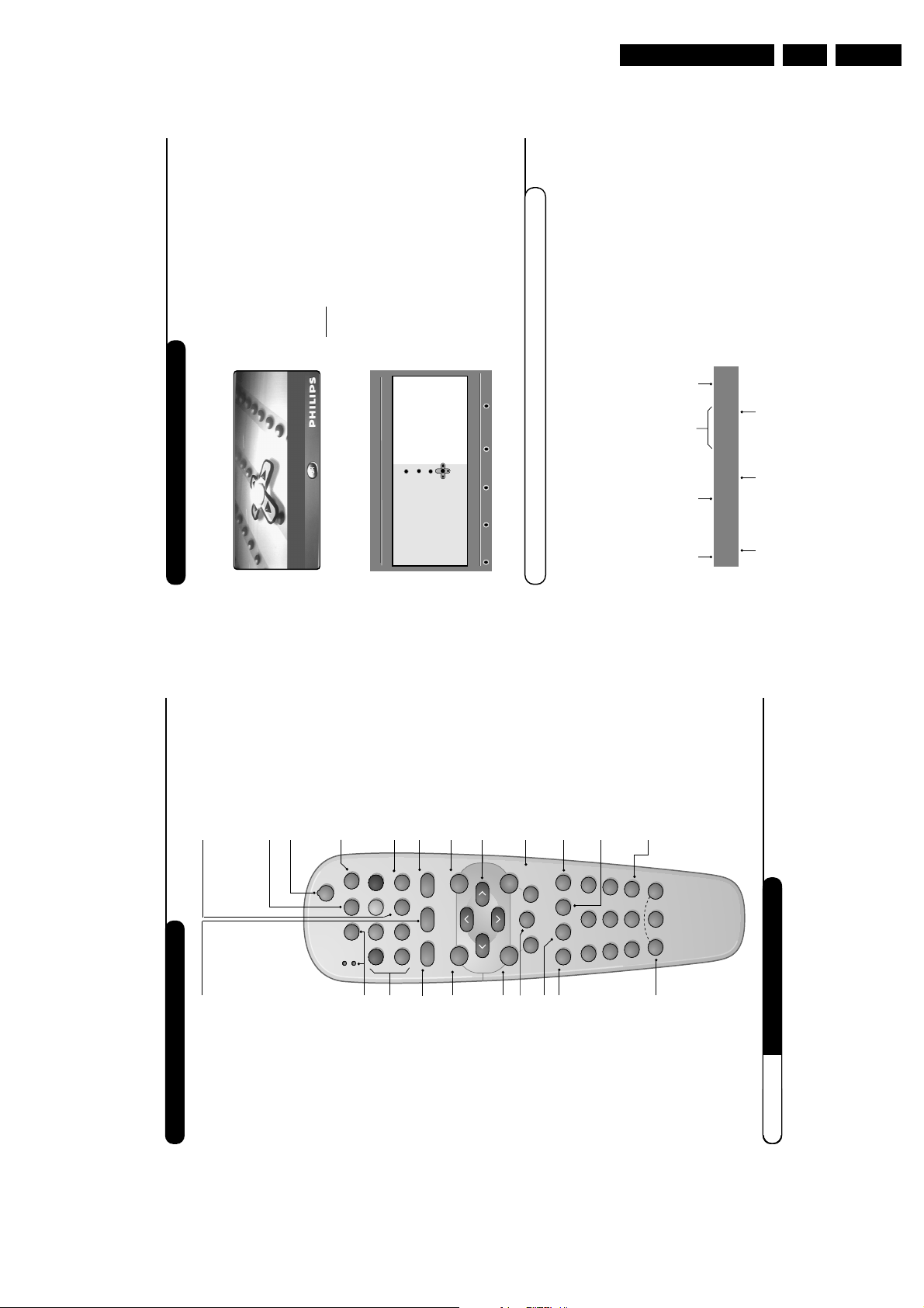
EN 2 A10E BB1.
Technical Specifications, Connections, and Chassis Overview
1. Technical Specifications, Connections, and Chassis Overview
1.1 Technical Specifications
1.1.1 Vision
Display type : Direct View CRT
: Real Flat
: 16:9
Screen size : 28” (70 cm)
: 32" (82 cm)
Tuning system : PLL
Colour systems : PAL: B/G, D/K, I
: SECAM: B/G,D/K,L/L’
: NTSC: playback only
Channel selections : 100 presets
: UVSH
IF Frequency : 38.9 MHz
Aerial input : 75 ohm, IEC-type
1.1.2 Sound
Sound systems : Bi NICAM B/G
: 2CS B/G
: FM/FM B/G
: NICAM B/G
: NICAM D/K
: NICAM I
: NICAM L
Maximum power : 2 x 10 W_rms (int.)
1.1.3 Miscellaneous
Mini Jack: Headphone - Out
Bk- Headphone 32 - 600 ohm / 10 mW ot
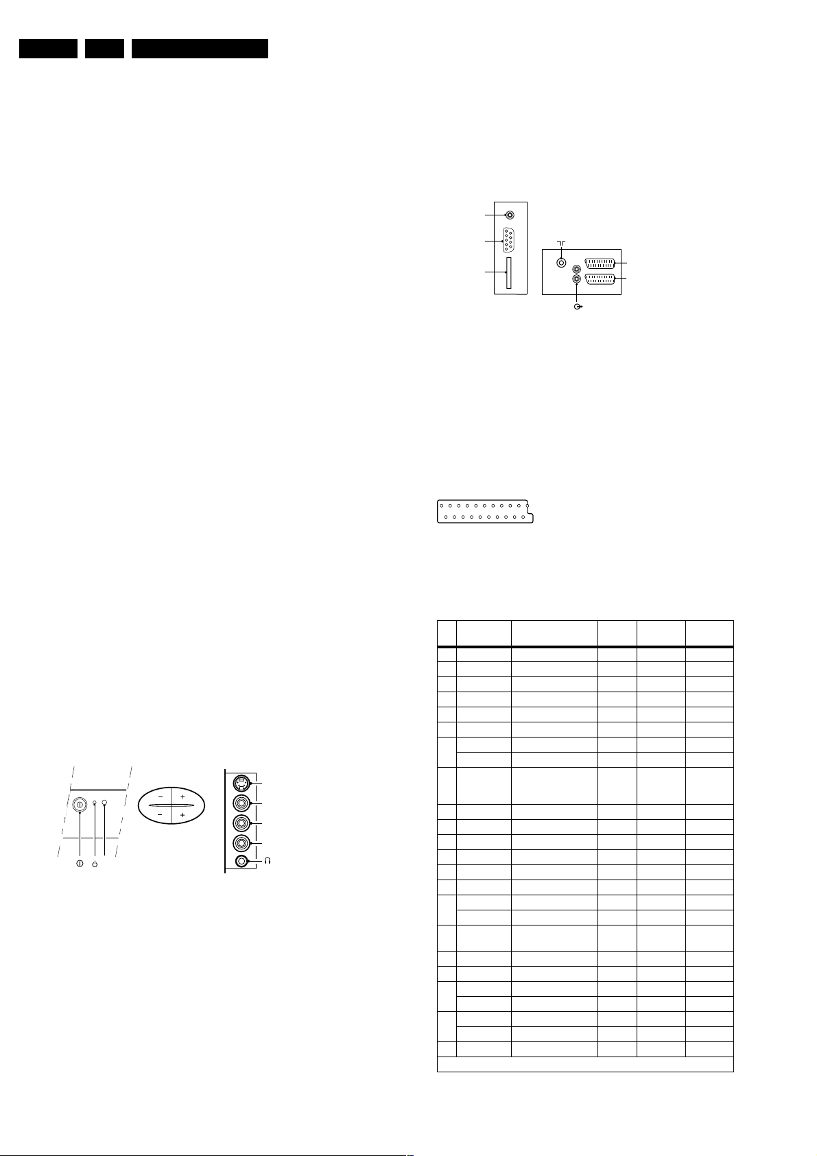
1.2.2 Rear Connections
DIGITAL OUT
RS232
SMART
CARD
AERIAL IN
L
R
AUDIO OUT
EXT2
EXT1
CL 36532080_064.eps
091203
Figure 1-2 Rear View
Aerial - In
- - IEC-type Coax, 75 ohm D
Cinch: Audio - Out
Rd- Audio - R 0.5 V_rms / 1 kohm kq
Wh-Audio - L 0.5 V_rms / 1 kohm kq
SCARTs
121
CL96532137_056.eps
202
171199
Mains voltage : 220 - 240 V
Mains frequency : 50 / 60 Hz
Ambient temperature : +5 to +45 deg. C
Maximum humidity : 90 % R.H.
Power consumption :
- Normal operation : ≈ 130 W
- Standby : < 11 W
1.2 Connections
1.2.1 Front View / Side Connections
FRONT + TOP CONTROL
- VOLUME +
- PROGRAM +
IR
RED
Figure 1-1 Front View and Side I/O
Hosiden: SVHS - In
1 - Y Ground H
2 - C Ground H
3 - Y 1 Vpp / 75 ohm j
4 - C 0.3 Vpp / 75 ohm j
Cinch: In
Ye- CVBS 1 Vpp / 75 ohm jq
Wh-Audio - L 0.5 V_rms / 10 kohm jq
R -Audio - R 0.5 V_rms / 10 kohm jq
SIDE I/O
S-Video
Video
L
Audio
R
CL 36532080_063.eps
271103
Figure 1-3 SCART connector
Table 1-1 SCART connection overview
j
j
EXT1
CVBS RGB
x / -
Pin Signal Signal level Type
1 Audio - R 0.5 V_rms / 1 kohm k xx
2 Audio - R 0.5 V_rms / 10 kohm j xx
3 Audio - L 0.5 V_rms / 1 kohm k xx
4 Audio - Gnd Ground H xx
5 Blue - Gnd Ground H x
6 Audio - L 0.5 V_rms / 10 kohm j xx
7 Blue / U 0.7 V_pp / 75 ohm j x / -
C-out 0.3 V_pp / 75 ohm k
8 CVBS-status 0 - 2 V: INT
9 Green - Gnd Ground H x
10 P50 Easylink jk
11 Green / Y 0.7 V_pp / 75 ohm j x / 12 N.C.
13 Red - Gnd Ground H xx
14 FBL - Gnd Ground H x
15 Red / V 0.7 V_pp / 75 ohm j x / -
C-in 0.3 V_pp / 75 ohm j x
16 Status / FBL 0 - 0.4 V: INT 1
17 Video - Gnd Ground H xx
18 Video - Gnd Ground H xx
19 CVBS-out 1 V_pp / 75 ohm k xx
Y-out 1 V_pp / 75 ohm k
20 CVBS-in 1 V_pp / 75 ohm j xx
Y-in 1 V_pp / 75 ohm j x
21 Shielding Ground H xx
x = connected, - = not used
4.5 - 7 V: EXT 16:9
9.5 - 12 V: EXT 4:3
- 3 V: EXT / 75 ohm
EXT2
CVBS Y/C
xx
Page 3
RS232
Technical Specifications, Connections, and Chassis Overview
EN 3A10E BB 1.
1
6
5
9
Figure 1-4 RS232 connector (sub-D 9p)
1 - DCD Data Carrier Detect j
2 - RXD Received Data j
3 - TXD Transmitted Data k
4 - DTR Data Terminal Ready k
5 - Ground
6 - DSR Data Set Ready j
7 - RTS Request To Send k
8 - CTS Clear To Send j
9-N.C.
Digital -out (coaxial)
Bk- S/PDIF k
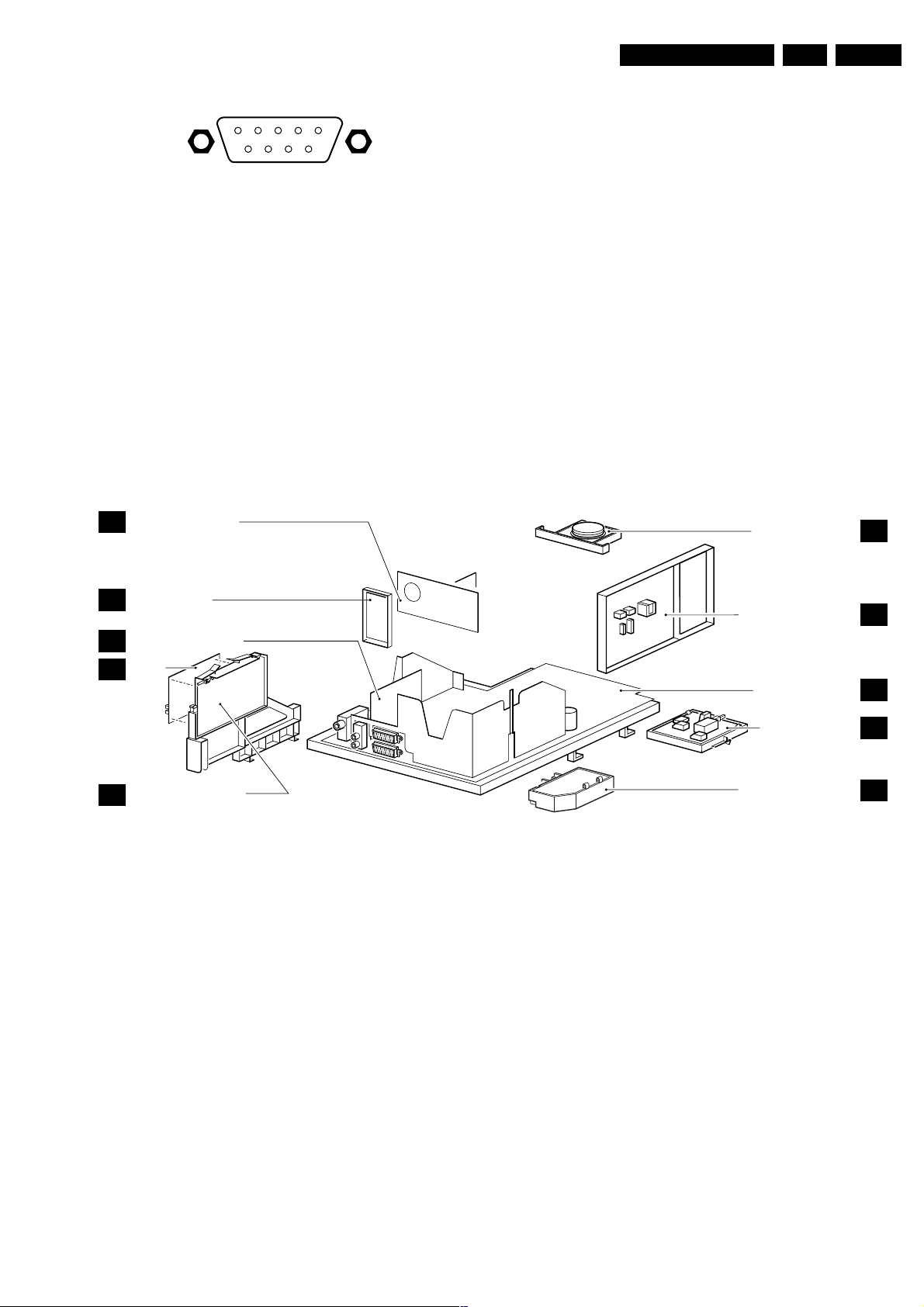
1.3 Chassis Overview
CRT/SCAVEM PANEL
B
TOP CONTROL PANEL
T
SIDE I/O PANEL
D
SMALL SIGNAL BOARD
C
+
IBO
K
PANEL
+
IBO
S
POWER SUPPLY &
DIGITAL INT. PANEL
Figure 1-5 PWB location
DC SHIFT & DAF PANEL
LARGE SIGNAL PANEL
MAINSWITCH PANEL
MAINS HARMONIC PANEL
CL 36532080_065.eps
G
A
J
U
121203
Page 4
EN 4 A10E BB2.
s
1
Safety and Maintenance Instructions, Warnings, and Notes
2. Safety and Maintenance Instructions, Warnings, and Notes
2.1 Safety Instructions
Safety regulations require that during a repair:
• Due to the chassis concept, a very large part of the circuitry
(incl. deflection) is 'hot'. Therefore, connect the set to the
mains via an isolation transformer.
• Replace safety components, indicated by the symbol h,
only by components identical to the original ones. Any
other component substitution (other than original type) may
increase risk of fire or electrical shock hazard.
• Wear safety goggles when you replace the CRT.
Safety regulations require that after a repair, you must return
the set in its original condition. Pay, in particular, attention to
the following points:
• General repair instruction: as a strict precaution, we advise
you to re-solder the solder connections through which the
horizontal deflection current is flowing. In particular this is
valid for the:
1. Pins of the line output transformer (LOT).
2. Fly-back capacitor(s).
3. S-correction capacitor(s).
4. Line output transistor.
5. Pins of the connector with wires to the deflection coil.
6. Other components through which the deflection current
flows.
Note: This re-soldering is advised to prevent bad connections
due to metal fatigue in solder connections, and is therefore only
necessary for television sets more than two years old.
• Check the insulation of the mains cord for external
damage.
• Check the strain relief of the mains cord for proper function,
to prevent the cord from touching the CRT, hot
components, or heat sinks.
• Check the electrical DC resistance between the mains plug
and the secondary side (only for sets that have an isolated
power supply). Do this as follows:
1. Unplug the mains cord and connect a wire between the
two pins of the mains plug.
2. Turn on the main power switch (keep the mains cord
unplugged!).
3. Measure the resistance value between the pins of the
mains plug and the metal shielding of the tuner or the
aerial connection of the set. The reading should be
between 4.5 Mohm and 12 Mohm.
4. Switch the TV 'off' and remove the wire between the
two pins of the mains plug.
• Check the cabinet for defects, to prevent the possibility of
the customer touching any internal parts.
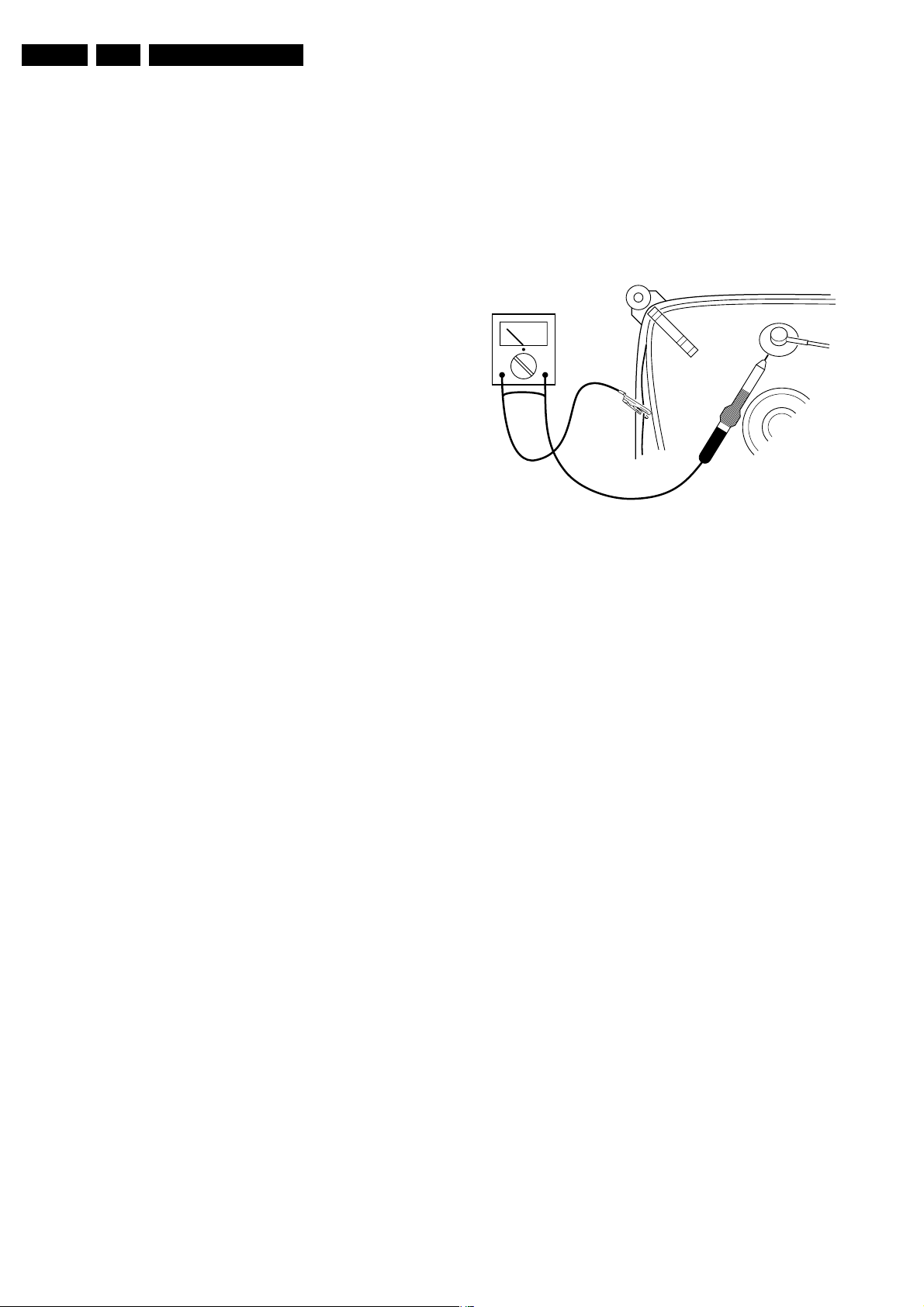
2.3 Warnings
• In order to prevent damage to ICs and transistors, avoid all
high voltage flashovers. In order to prevent damage to the
picture tube, use the method shown in Fig. 2-1, to
discharge the picture tube. Use a high voltage probe and a
multi-meter (position V_dc). Discharge until the meter
reading is 0 V (after approx. 30 s).
V
Figure 2-1 Discharge picture tube
• All ICs and many other semiconductors are susceptible to
electrostatic discharges (ESD, w). Careless handling
during repair can reduce life drastically. Make sure that,
during repair, you are connected with the same potential as
the mass of the set by a wristband with resistance. Keep
components and tools also at this potential. Available ESD
protection equipment:
– Complete kit ESD3 (small tablemat, wristband,
connection box, extension cable and ground cable)
4822 310 10671.
– Wristband tester 4822 344 13999.
• Together with the deflection unit and any multi-pole unit,
flat square picture tubes form an integrated unit. The
deflection and the multi-pole units are set optimally at the
factory. We do not recommend adjusting this unit during
repair.
• Be careful during measurements in the high voltage
section and on the picture tube.
• Never replace modules or other components while the unit
is 'on’.
• When you align the set, use plastic rather than metal tools.
This will prevent any short circuits and the danger of a
circuit becoming unstable.
CL96532156_040.ep
14050
2.2 Maintenance Instructions
We recommend a maintenance inspection carried out by
qualified service personnel. The interval depends on the usage
conditions:
• When a customer uses the set under normal
circumstances, for example in a living room, the
recommended interval is three to five years.
• When a customer uses the set in an environment with
higher dust, grease, or moisture levels, for example in a
kitchen, the recommended interval is one year.
• The maintenance inspection includes the following actions:
1. Perform the 'general repair instruction' noted above.
2. Clean the power supply and deflection circuitry on the
chassis.
3. Clean the picture tube panel and the neck of the picture
tube.
• The picture tube panel has printed spark gaps. Each spark
gap is connected between an electrode of the picture tube
2.4 Notes
2.4.1 General
• Measure the voltages and waveforms with regard to the
chassis (= tuner) ground (H), or hot ground (I), depending
on the tested area of circuitry.
• The voltages and waveforms shown in the diagrams are
indicative. Measure them in the Service Default Mode (see
chapter 5) with a colour bar signal and stereo sound (L: 3
kHz, R: 1 kHz unless stated otherwise) and picture carrier
at 475.25 MHz (PAL) or 61.25 MHz (NTSC, channel 3).
• Where necessary, measure the waveforms and voltages
with (D) and without (E) aerial signal. Measure the
voltages in the power supply section both in normal
operation (G) and in standby (F). These values are
indicated by means of the appropriate symbols.
and the Aquadag coating.
Page 5

Safety and Maintenance Instructions, Warnings, and Notes
EN 5A10E BB 2.
• The semiconductors indicated in the circuit diagram and in
the parts lists, are interchangeable per position with the
semiconductors in the unit, irrespective of the type
indication on these semiconductors.
• Manufactured under license from Dolby Laboratories.
‘Dolby’, ‘Pro Logic’ and the ‘double-D symbol’, are
trademarks of Dolby Laboratories.
Figure 2-2 Dolby PL Symbol
2.4.2 Schematic Notes
• All resistor values are in ohms and the value multiplier is
often used to indicate the decimal point location (e.g. 2K2
indicates 2.2 kohm).
• Resistor values with no multiplier may be indicated with
either an "E" or an "R" (e.g. 220E or 220R indicates 220
ohm).
• All capacitor values are expressed in micro-farads (µ= x
10^-6), nano-farads (n= x 10^-9), or pico-farads (p= x 10^-
12).
• Capacitor values may also use the value multiplier as the
decimal point indication (e.g. 2p2 indicates 2.2 pF).
• An "asterisk" (*) indicates component usage varies. Refer
to the diversity tables for the correct values.
• The correct component values are listed in the Electrical
Replacement Parts List. Therefore, always check this list
when there is any doubt.
To reflow the solder, apply a temperature profile according to
the IC data sheet. So as not to damage neighbouring
components, it may be necessary to reduce some
temperatures and times
2.4.3 Rework on BGA (Ball Grid Array) ICs
General
Although (LF)BGA assembly yields are very high, there may
still be a requirement for component rework. By rework, we
mean the process of removing the component from the PWB
and replacing it with a new component. If an (LF)BGA is
removed from a PWB, the solder balls of the component are
deformed drastically so the removed (LF)BGA has to be
discarded.
Device removal
As is the case with any component that, it is essential when
removing an (LF)BGA, the board, tracks, solder lands, or
surrounding components are not damaged. To remove an
(LF)BGA, the board must be uniformly heated to a temperature
close to the reflow soldering temperature. A uniform
temperature reduces the chance of warping the PWB.
To do this, we recommend that the board is heated until it is
certain that all the joints are molten. Then carefully pull the
component off the board with a vacuum nozzle. For the
appropriate temperature profiles, see the IC data sheet.
Area preparation
When the component has been removed, the vacant IC area
must be cleaned before replacing the (LF)BGA.
Removing an IC often leaves varying amounts of solder on the
mounting lands. This excessive solder can be removed with
either a solder sucker or solder wick. The remaining flux can be
removed with a brush and cleaning agent.
After the board is properly cleaned and inspected, apply flux on
the solder lands and on the connection balls of the (LF)BGA.
Note: Do not apply solder paste, as this has shown to result in
problems during re-soldering.
Device replacement
The last step in the repair process is to solder the new
component on the board. Ideally, the (LF)BGA should be
aligned under a microscope or magnifying glass. If this is not
possible, try to align the (LF)BGA with any board markers.
Page 6
EN 6 A10E BB3.
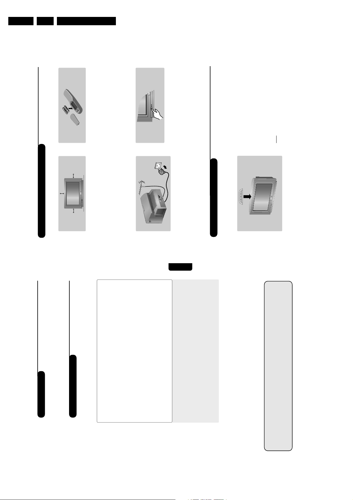
The television set has 4 keys which are
located on the front or the top of the set
depending on the model.
The VOLUME - + (-
”
+) keys are used to
adjust sound levels.
The PROGRAM - + (- P +) keys are used to
select the required programmes.
To access the menus,simultaneously hold
down the
”
- and
”
+ keys.The
PROGRAM - + keys may then be used to
select an adjustment and the -
”
+ keys to
make that adjustment.
To exit from the menus,hold down
the 2
”
- and
”
+ keys.
Note
: when the CHILD LOCK function is activated,
these keys are unavailable (refer to FEATURES
menu on page 14).
PROGRAMVOLUME
--
++
2
&
Positioning the television set
Place your TV on a solid,stable surface, leaving
a space of at least 5 cm around the appliance.
To avoid accidents,do not put anything on the
set such as a cloth or cover, a container full of
liquid (vase) or a heat source (lamp).The set
must not be exposed to water.
é
Connections
• Insert the aerial plug into the
:
socket at
the rear of the set.
• Insert the mains plug into a wall socket (220-
240 V / 50 Hz).
“
Remote control
Insert the two R6-type batteries (supplied)
making sure that they are the right way round.
The batteries supplied with this appliance do not
contain mercury or nickel cadmium. If you have
access to a recycling facility,please use this facility
(if in doubt, consult your dealer).When the batteries
are replaced, use the same type.
‘
Switching on
To switch on the set,press the on/off key.
A red indicator comes on and the screen
lights up. Go straight to the chapter Switch
on for the first time, on page 4.
If the television remains in standby mode,
press P
#
on the remote control.
The indicator will flashe when you use the remote
control.
5 cm
5 cm
Installing your television set
The keys on the TV set
ANALOGUE MENUS
1
Introduction
Table of Contents
Thank you for purchasing this television set.
This handbook has been designed to help you install and operate your TV set.
We would strongly recommend that you read it thoroughly.
We hope this new television meets entirely with your satisfaction.
Installing your television set . . . . . . . . . . . . . . . . . . . . . . . . . . . . . . . . . . . . . . . . . .2
The keys on the TV set . . . . . . . . . . . . . . . . . . . . . . . . . . . . . . . . . . . . . . . . . . . . . .2
The remote control keys . . . . . . . . . . . . . . . . . . . . . . . . . . . . . . . . . . . . . . . . . . . .3
Digital or Analogue channels ? . . . . . . . . . . . . . . . . . . . . . . . . . . . . . . . . . . . . . . . . .3
Switch on for the first time . . . . . . . . . . . . . . . . . . . . . . . . . . . . . . . . . . . . . . . . . .4
Understanding the information on the banner . . . . . . . . . . . . . . . . . . . . . . . . . . .4
Rearrange TV channels / radio station . . . . . . . . . . . . . . . . . . . . . . . . . . . . . . . . . .5
View or Listen new TV services . . . . . . . . . . . . . . . . . . . . . . . . . . . . . . . . . . . . . . .5
List Channel types . . . . . . . . . . . . . . . . . . . . . . . . . . . . . . . . . . . . . . . . . . . . . . . . .5
Add new services . . . . . . . . . . . . . . . . . . . . . . . . . . . . . . . . . . . . . . . . . . . . . . . . . .6
Reinstall all services . . . . . . . . . . . . . . . . . . . . . . . . . . . . . . . . . . . . . . . . . . . . . . . .6
Test reception . . . . . . . . . . . . . . . . . . . . . . . . . . . . . . . . . . . . . . . . . . . . . . . . . . . . .6
Language and location preferences . . . . . . . . . . . . . . . . . . . . . . . . . . . . . . . . . . . .7
Access restrictions . . . . . . . . . . . . . . . . . . . . . . . . . . . . . . . . . . . . . . . . . . . . . . . . .7
Setting up your favourite list . . . . . . . . . . . . . . . . . . . . . . . . . . . . . . . . . . . . . . . . .8
Informations menu . . . . . . . . . . . . . . . . . . . . . . . . . . . . . . . . . . . . . . . . . . . . . . . . . .8
Downloading new software . . . . . . . . . . . . . . . . . . . . . . . . . . . . . . . . . . . . . . . . . . .8
Using the Options menu . . . . . . . . . . . . . . . . . . . . . . . . . . . . . . . . . . . . . . . . . . . .9
TV guide . . . . . . . . . . . . . . . . . . . . . . . . . . . . . . . . . . . . . . . . . . . . . . . . . . . . . . . . .9
Recording function . . . . . . . . . . . . . . . . . . . . . . . . . . . . . . . . . . . . . . . . . . . . . . . .10
Automatic tuning of analogue programmes . . . . . . . . . . . . . . . . . . . . . . . . . . . . .11
Sorting analogue programmes . . . . . . . . . . . . . . . . . . . . . . . . . . . . . . . . . . . . . . .11
Manual tuning of analogue programmes . . . . . . . . . . . . . . . . . . . . . . . . . . . . . . . .12
Naming analogue programmes . . . . . . . . . . . . . . . . . . . . . . . . . . . . . . . . . . . . . . .12
EasyLink function . . . . . . . . . . . . . . . . . . . . . . . . . . . . . . . . . . . . . . . . . . . . . . . . . .12
Adjusting the picture . . . . . . . . . . . . . . . . . . . . . . . . . . . . . . . . . . . . . . . . . . . . . .13
Adjusting the sound . . . . . . . . . . . . . . . . . . . . . . . . . . . . . . . . . . . . . . . . . . . . . . .13
Rotating the picture . . . . . . . . . . . . . . . . . . . . . . . . . . . . . . . . . . . . . . . . . . . . . . .13
Timer function . . . . . . . . . . . . . . . . . . . . . . . . . . . . . . . . . . . . . . . . . . . . . . . . . . . .14
Locking the set . . . . . . . . . . . . . . . . . . . . . . . . . . . . . . . . . . . . . . . . . . . . . . . . . . .14
Analogue Teletext . . . . . . . . . . . . . . . . . . . . . . . . . . . . . . . . . . . . . . . . . . . . . . . . .15
Digital Text . . . . . . . . . . . . . . . . . . . . . . . . . . . . . . . . . . . . . . . . . . . . . . . . . . . . . .16
16:9 Formats . . . . . . . . . . . . . . . . . . . . . . . . . . . . . . . . . . . . . . . . . . . . . . . . . . . . .16
Connecting peripheral equipment . . . . . . . . . . . . . . . . . . . . . . . . . . . . . . . . . . . .17
To select connected equipment . . . . . . . . . . . . . . . . . . . . . . . . . . . . . . . . . . . . .17
VCR / DVD mode selector . . . . . . . . . . . . . . . . . . . . . . . . . . . . . . . . . . . . . . . . .18
Glossary . . . . . . . . . . . . . . . . . . . . . . . . . . . . . . . . . . . . . . . . . . . . . . . . . . . . . . . .19
Tips . . . . . . . . . . . . . . . . . . . . . . . . . . . . . . . . . . . . . . . . . . . . . . . . . . . . . . . . . . . .19
Centre Frequencies Table (in KHz) . . . . . . . . . . . . . . . . . . . . . . . . . . . . . . . . . . . .20
DIGITAL MENUS
°
Recycling
The materials used in your set are either reusable or can be recycled.
To minimise environmental waste,specialist companies collect used appliances
and dismantle them after retrieving any materials that can be used again (ask
your dealer for further details).
English
3. Directions for Use
Directions for Use
Page 7
Directions for Use
4
The first time the TV set is switched on, a
congratulation
message will appear on screen.
The language of which changes every 5 seconds.
&
Press the
u
key on the remote control,the
moment your prefered language is visible
on the screen.The
Setup
menu is displayed :
é The
language
, corresponding
country
and
time
zone
is now preselected according to the
opening screen. However, you can still change
your preferences before you start a service
scan.
“ With the cursor keys, select
language
,
country
or
Time zone
and check if the adjustment is
according to your preferences.If necessary,
use the cursor keys to make your adjustment
and press
u
to exit.
Caution
: if you select a wrong country, the channel
numbering will not be according to the standard
for your country.
‘ Select
service scan
from the menu and press
u
to start the installation.The
service scan
menu is displayed.All the digital and analogue
programmes are search for and stored
automatically.When the search is complete,
the menu will indicate the number of digital
services and analogues programmes found.
( Press the
u
key to start watching TV.
The television then displays the current
programme.The installation is now complete.
When you select a digital programme, an
information banner is displayed for a few
secondes at the top of the screen.
You can also use the
∂
key of the remote
control to display this banner.A second press
displays more information about the programme
(when available).
The banner contains information on the
preset number, channel name, programme
duration, transmission clock,programme title
and the time remaining of the current
programme (if set in the options menu).
Switch on for the first time
Understanding the information on the banner
Setup
Start service scan
Language
Country
Time Zone
Service Scan
11:46
Please press OK to start
Congratulations for selecting this Philips television.
Press OK to start enjoying your digital television.
2 11:06 - 11:09
BBC2 Snooker
11:46
Minutes left : 14
u
ù
i
ß
preset
number
symbols
clock
programme
start and end
time
remaining time
of programme
programme titlechannel name
Symbols description :
i more information about this programme
is available : press the
∂
key to display
or remove it.
ß subtitling is available : if you want to
display them,press the
OPTIONS
key to
access the
options
menu and select
subtitles.
ù other audio languages are availables and
can be selected in the
options
menu.
u the selected Favourite list is displayed in
the colour of the activated list.
Banner description:
3
12
MODE
BACK
VCR
DVD
MENU
OK
A/D
”
P(age)
564
879
0
·¢Ê Æ
∫
†
¤
Œ
Á
ª
-
`
Å
3
--
++
.
DIGITAL
TV
[
Ø
EXIT/OPTIONS
›
Ó
Ω
%
ù
Ë
MENU
SELECT
∏
Ÿ
SMART
SMART
SOUND
PICTURE
The remote control keys
Screen information
In digital mode, press onece to display
the information banner,a 2
nd
time to get
more information on the programme
and a 3rd time to remove it (see p.4).
In analogue mode, this displays /
removes the programme informations
(number,name, time, sound mode).Hold
down for 5 seconds to permanently
display the analogue programme
number on the screen.The volume level
and the smart control adjustments are
then displayed each time they are used.
Options menu
(see p.8).
Teletext features (p.15)
and VCR/DVD keys (p.18).
TV Menu
To display or exit from the analogues
menus
Select
In digital mode this displays / clears the
programme list.Use the
îÏ
keys
to select a programme and the
¬
(or
u
) key to display it.
Volume
To adjust the sound level
16:9 formats (p.16)
Mute
To disable or enable the sound.
Picture and sound settings
Accesses a series of picture and
sound settings.
The position PERSONAL corresponds to
the settings stored in the menus.
Sound mode
To switch from
STEREO
to
MONO
or to choose between different
languages (Dual I, Dual II,...).
When the sound mode is switched to
MONO
, the indication is displayed in red.
Select EXT sockets
(see p.17).
Standby
To set the TV to standby mode.To
switch the TV set on again, press
P
@#
or
09
.
TV guide
(see p.9).
Program list (analogue mode)
To display/clear the program list.
Use the
îÏ
keys to select a
programme and
¬
to display it.
Digital Menu
To display or exit from the digital
menus (when TV is in digital mode).
Analogue or Digital mode
To switch the television vetween
analogue and digital mode.
Cursor
These 4 keys are used to move
within the menus or to directly access
the 16:9 screen formats (p 16).
Surround sound
To activate / deactivate the Virtual
Dolby Surround * effect.In stereo, you
can obtain Dolby Surround
Pro Logic sound quality.In mono, a
stereo spatial effect is simulated.
*
Manufactured under license from Dolby Laboratories.
”Dolby” ”Pro Logic”and the double-D symbol are
trademarks of Dolby Laboratories.
Previous programme
To access the previously viewed
programme.
Sleeptimer
To select the length of time before
the set automatically switches to
standby (from 0 to 240 minutes)
Numerical keys
For direct access to programmes.
For a 2 (3) digit programme number,
the 2
nd
(3
rd
)digit must be entered
before the dash disappears.
The number,the name (and the sound
mode, in analogue mode) are
displayed for a few seconds.
Programme selection
To access the next or previous
programme (or page in digital menus).
Mode selector
To activate the remote control in
VCR or DVD mode (see p.18).
To receive TV channels,your television is equipped with 2 tuners. One is for digital channels,the other
is for analogue channels. Use the
v
key of the remote control to swhitch the TV between analogue
and digital mode.Then use the
P @#
or
09
keys to select channels.
Digital or Analogue channels ?
EN 7A10E BB 3.
Page 8
EN 8 A10E BB3.
6
Add new services
This menu allows you to search for new TV
channels or radio stations that have been launched
by the broadcaster after the initial installation.
& From digital mode, press the
‹ MENU
key to
display the setup menu.
é Use the
Ï
key to select
installation
and press
¬
.
“ Select
Service setup
(
Ï
) and press
¬
.
‘ Press
¬
to select
Add new services
and
press
u
to activate the installation.
The search begins and only new channels will
be stored and added to the
channel list
menu.
The percentage of the installation that has
been completed and the number of channels
found is displayed.
( When the search is complete, select store and
press
u
to accept the new services.
§ Press the
‹ MENU
key to leave the menu.
This menu allows you to reinstall all the digital
TV channels and radio stations.
& From digital mode, press the
‹ MENU
key to
display the setup menu.
é Use the
Ï
key to select
installation
and press
¬
.
“ Select
Service setup
(
Ï
) and press
¬
.
‘ Select
Reinstall all services
(
Ï
) and press
¬
.
( Press
u
to start the installation.
A search is then made for all digital services
which are then stored automatically.
When the search is completed, the menu will
indicate the number of digital services found.
§ When the search is complete, press
u
to
store the services.
è Press the
‹ MENU
key to leave the menu.
This menu allows you to check the strengh of
the signal you are receiving through your aerial.
& From digital mode, press the
‹ MENU
key to
display the setup menu.
é Use the
Ï
key to select
installation
and press
¬
to display the installation menu.
“ Use
Ï
to select
Test reception
and press
¬
.
You obtain an indication of the actual
programme frequency, the network name, the
signal quality and strength.
‘ You now have to enter the frequency of the
digital channel you want to test.
Your Tv magazine can provide the list of digital
channel numbers. Use the table on page 20 to get
the frequency.
( If the signal quality and strength is poor, a
message appears at the bottom of the menu
prompting you to enter the frequency between
the lower and the higher limit. If after keying
the frequency,the reception is still poor,you
can try improving, renewing, adjusting or
updating the aerial. It is however advisable to
contact a specialised aerial installer in order to
achieve best results.
Reinstall all services
Test reception
Setup
Installation
Test signal quality
Close
Service lists
Service setup
Test reception
11:46
Frequency
Network name
Signal quality
Signal strength
Setup
Installation
Install and manage services
Close
Service lists
Service setup
Test reception
11:46
Add new services
Reinstall all services
5
Rearrange TV channels / radio station
This menu allows you to change the order of
the stored digital channels or radio station.
& From digital mode, press the
‹ MENU
key to
display the setup menu.
é Use the
Ï
key to select
installation
and press
¬
twice to select the
Service lists
menu.
“ Use the
îÏ
keys to select
Rearrange TV
channels
or
Rearrange radio stations
and
press
¬
.
‘ Use the
îÏ
keys to select the channel you
want to exchange.
( Press
u
to activate.
If you want to uninstall the selected channel, press
the red key.
§ Select (
îÏ
) the new channel number you
want to exchange it with.
è Press
u
to confirm.The exchange is done.
! Repeat the operations ‘ to è until all the
channels are in the required order.
ç Press the
‹ MENU
key to leave the menu.
This menu allows you to check the availability
of new TV channels or new radio stations that
have been launched by the broadcaster after
the initial installation.
& From digital mode, press the
‹ MENU
key to
display the setup menu.
é Use the
Ï
key to select
installation
and press
¬
twice to select the
Service lists
menu.
“ Use the
îÏ
keys to select
View new TV
channels
or
Listen to new Radio station
.
‘ If new services are availables,press
¬
to
enter into the list and use the îÏ keys to
move through the list.
( Press the
‹ MENU
key to leave the menu.
This menu allows you to restore the original
list of channels defined by the broadcaster
during the initial installation.
& From digital mode, press the
‹ MENU
key to
display the setup menu.
é Use the
Ï
key to select
installation
and press
¬
twice to select the
Service lists
menu.
“ Use the
îÏ
keys to select
List channel
types
and press
¬
.
‘ Select
Original list of channels
and press
u
if
you want to restore the original list of
channels defined by the broadcaster.
Remar
k: when this option is set,it is not possible to
rearrange TV channels or radio stations.
( Select
User-definable list of services
and press
u
if you want to get your prefered channel
list.
§ Press the
‹ MENU
key to leave the menu.
View or Listen to new services
List Channel types
Setup
Installation
Manage service lists
Close
Service lists
Service setup
Test reception
11:46
Rearrange TV channels
List channel types
View new TV channels
Rearrange Radio stations
Listen to new Radio stations
Directions for Use
Page 9
Directions for Use
8
Setting up your favourite list
This menu enables you to create a favourite
list with your prefered TV channels and radio
stations. For example, each member of your
family can create his/her own favourite list.
& From digital mode, press the
‹ MENU
key to
display the setup menu.
é Press
¬
to enter into the
favourites
list
menu.You have the choice to create 4 different
favourite lists.
“ Use the
Ïî
keys to select your favourite
list :
List 1
,
List 2
,
List 3
or
List 4
and press
¬
.
‘ Use the
Ïî
keys to select a setting and
press
¬
to enter into the sub-menu.
•
Name
: use the
Ȭ
keys to move around
the name display area (15 characters) and the
@
P
#
keys to select the characters.When
the name has been entered, press
u
to exit.
•
Select TV channels
: use the
Ïî
keys to
select your favourite TV channels and confirm
with
u
. Press
È
to exit.
•
Select radio stations
: use the
Ïî
keys to
select your favourite radio station and
confirm with
u
. Press
È
to exit.
•
Add all services
: press
u
if you want to add
all the service into your favourite list.
•
Remove all services
: press
u
if you want to
remove all the service from your favourite list.
( Press the
‹ MENU
key to leave the menu.
§ Your favourite list can be selected using the
options
menu (see next page).
This menu provides informations about the
software version,the installation of new
software and problem reports.
& From digital mode, press the
‹ MENU
key to
display the setup menu.
é Use the
Ï
key to select
information
and
press
¬
.
“ Select
Problem reports
and press
¬
to
access any reported errors.In the event of a
technical problem, your tv service organisation
might ask you to tell them if there are any
reports and what they say.
‘ Select
System software
and press
¬
.The
software version is displayed.
( You can activate the menu to automatically
accept any software update of your digital TV.
Normally the product will detect if an update is
available while it is in standby mode.Next time
the television is turned on a banner will appear
at the bottom of the screen indicating new
software is available.Selecting
u
activates the
software download.The software download
menu will give a description of the software
together with the date and time of the
download.This may update certain menus,
functions or add new features,but the general
way in which the TV operate will not change.
Once accepted the download will take place at
the designated time and date.
Note
:The TV must be put into standby when the
download is due in order for it to take place.
§ Press the
‹ MENU
key to leave the menu.
Information
Downloading new software
Setup
Make changes to your list of favourites services
Favourites
Preferences
Information
Access restrictions
Installation
11:46
List 1
List 2
List 3
List 4
Setup
Make changes to your list of favourites services
Favourites
Preferences
Information
Access restrictions
Installation
11:46
System software
Problem reports
Whenever a new software is available,
it is advisable to always accept
and download the software.
In case new software is available,you will see a message when you switch on the TV.
7
Language and location preferences
This menu allows you to select your prefered
language for audio,subtitle, teletext and menu
and make changes to the location (country
and time zone).
& From digital mode, press the
‹ MENU
key to
display the setup menu.
é Use the
Ï
key to select
preferences
and
press
¬
.
“ Select
Languages
or
Location
(
Ï
) and press
¬
.
‘ Use the
Ïî
keys to select a setting and
press
¬
to enter into the sub-menu. Make
your adjustment and press
u
or
È
to exit.
Language default settings:
•
Audio
: to select the audio sound language.
•
Subtitle
: to select the subtitle language.
•
Subtitles for hearing impaired
: to activated or
deactivate the specific subtitle for hearing
impaired (if made available by the broadcaster).
•
Teletext
: to select the teletext language.
•
System
: to select the menu language.
Location settings:
•
Country
: to select the country where you are
located.
•
Time zone
: to select the time zone where
you are located.
•
Daylight saving time
: to select automatic,
manual or no daylight saving time.
( Press the
‹ MENU
key to leave the menu.
This menu allows you to setup the access
restrictions of the digital channels.
& From digital mode, press the
‹ MENU
key to
display the setup menu.
é Use the
Ï
key to select
Access restriction
and press
¬
.
“ Press the
¬
key to enter into the
Set pin
code protection
menu.
‘ Use the
Ȭ
keys to set to
on
and press
u
to exit.You can then access to the other
adjustments :
W
arning: the moment you use any kind of access
restriction, you need to fill in the pin code when you
schedule a program for recording.
•
Maturity rating
: select your prefered rating to
lock the channel.
Maturity rating will only block certain programmes if
the broadcaster providedes with the programme.
•
System lock
: press
u
if you want to
completely lock the digital tv.To unlock, enter
your pin code (or the universal code 0711).
•
TV channels
: select the tv channel you want to
lock and press
u
.
•
Radio station
: select the radio station you
want to lock and press
u
.
•
Change pin code
: press
¬
to enter in the
menu. Follow the on-screen instruction to
change your access code.
The default pin code is 1234. If you have forgotten
your personal code, you can reset to the default pin
code (1234) by enter the universal code 0711.
( Press the
‹ MENU
key to leave the menu.
The TV is equipped with a Common Interface (CI)
slot (see p.18).A CI module can enable additional
services, for example Pay TV.The Access Restrictions
menu will show the CI Access Restrictions when a
CI module is installed.The CI module is responsible
for the messages and texts on screen. In case of
failure or strange behaviour,you must call your CI
service provider.
Access restrictions
Setup
Preferences
Select your prefered language
Close
Languages
Location
11:46
Audio
Subtitle
Hearing impaired subtitles
Teletext
System
Setup
Access restrictions
Switch pin code protection “on” or “off”
Close
Set pin code protection
System pin code settings
System lock
TV channels
Radio stations
System pin code
11:46
On Off
EN 9A10E BB 3.
Page 10
EN 10 A10E BB3.
10
Recording function
This feature enables you to program a digital
recording and control the VCR (if it has an
EasyLink feature and is connected to EXT2).
If your video recorder is not equipped with
Easylink, the TV will provide a digital channel
to be recorded.You will still need to program
your video recorder.
Important:The video recorder must be connected
to EXT2. Please note that it is NOT possible to record
one digital channel and watch another digital channel
at the same time.You can however record a digital
channel and watch an analogue channel on your TV, or
vice versa. Philips recorders with only the TV link
feature do not support easy recording : you wil still
have to program your VCR.
& From digital mode, press the
o
key to display
the TV guide.
é Press the
RED
key to call the Record menu.
“ Use the
Ïî
keys to select a setting and
press
¬
to enter into the sub-menu. Make
your adjustment and press
u
or
È
to exit.
• Service : you can change the number of the
programme you want to record.Press
u
to
confirm.
• Enter your pin code if locked : enter your
secret code only if you have activated the
access restriction feature (see p.7).Press
u
to confirm.
• Day & Month : enter the date by using the
09
or
@
P
#
keys.Press
u
to exit
• Start time : enter the start time.
• End time : enter the end time.
• Audio language : select your language and
confirm with
u
.
• Subtitle language : make your selection and
confirm with
u
.
• Subtitle for hearing impaired : select
Yes
or
No
and confirm with
u
.
• Occurence : select
Once
,
Daily
or
Weekly
and confirm with
u
.
‘ Press the
RED
key to store your recording.
The TV guide reappears.
You can press the
GREEN
key to display the list of
recordings you have set.
(
If your video recorder is not equipped with
Easylink feature, remember you still need to
program it.
§ If you have finished watching television, you must
leave it in standby in order for the recording
program to be activated.
Important: never switch off the TV with the power
button when a recording has been programmed,
but use the standby key on the remote control.
è If you wish to continue watching another
digital channel after setting a timer,you can do
so by changing channels in the normal way.
! If you are watching another digital channel when
the timer is due to start, the timer alarm will sound
and present you with the option of switching
channels or continuing to watch the current
channel.
ç You can also watch analogue channels while
recording digital channels. Press the
v
key to
switch the TV to analogue mode.
The moment a timer start, you get a warning
message and you can still decide to stop recording.
2 BBC 2
Please enter the preset number.
Close CancelStore
Service
Enter your pin code if locked
Day & Month
Start time
End time
Audio language
Subtitle language
11:46
2 BBC 2
16/02
12:15
12:30
English
none
9
Using the Options menu
This menu gives you direct access to the:
favourite list,the language selection and some
other selections.
& From digital mode, press the
EXIT/OPTIONS
key to
display the options menu.
é Use the
Ïî
keys to select a setting and
press
¬
to enter the sub-menu.
•
Favourites
: use the
Ïî
keys to select your
favourite list and confirm with
u
.
The “none”option deactive any favourite list.
To create your own favourite list, see page 8.
•
Subtitle language
: use the
Ïî
keys to
temporarily change the language and confirm
with
u
.
•
Subtitle for hearing impaired
: select
Yes
and
confirm with
u
to temporaly activate this
feature.
•
Audio language
: to temporarily change the
audio sound language.
To permanetly change the audio and subtitle
languages, use the Preferences menu (p.7).
•
Mode
: you can choose to only have
radio
stations,
TV
channels or
services without audio
or video
.
Remar
k: for the UK only, the TV list will contain both
radio stations and TV channels.
•
Show the remaining play time ?
: select
Yes
and
confirm with
u
if you want to display the
remaining play time when you call the banner.
•
banner duration
: to select the duration for
which the banner is visible.
“ Press the
EXIT/OPTIONS
key to leave the menu.
The TV guide is an Electronic Service Guide
that allows you to look up digital programmes
as you would in a newspaper or TV magazine.
You can navigate through the list of digital
programmes and obtain detailed information
on the programmes.You can also program the
TV to provide a digital channel to be recorded.
& From digital mode, press the
o
key to display
the TV guide :
A list with all the installed digital programmes
is displayed.
é Use the îÏ keys to select a programme.
“ The TV guide features are displayed at the
bottom of the screen. Use the coloured keys red,
green, yellow,blue or white to activate them :
• Record (red key) : this feature enables you to
program the recording of the video recorder
(if it has an EasyLink feature and is connected
to EXT2). If your video recorder is not
equipped with Easylink, the TV will provide a
digital channel to be recorded.You will still have
to program your video recorder.
• Record list (green key) : this menu gives the
list of recording schedules.You can check,
modify,delete or add a new schedule by using
the cursor or coloured keys as indicated on
the screen.
•
Information
(yellow key)
: you can obtain more
detailled information on the selected
programmes
.
• Close (blue key) : to exit from the TV guide.
• Options (white ∫ key) : with this menu, you
can select your favourite list,mode or themes.
Themes are areas of interest,you can for
example decide to display only :drama, news,
movie, ...
‘ Press the
o
key to leave the menu.
TV guide
Options
Selects the active favourite list
Exit
Favourites
Subtitle language
Subtitles for hearing
impaired
Audio language
None
List 1
List 2
List 3
List 4
Selects the active favourite list
OptionsCloseInformationRecord listRecord
1 BBC ONE
2 BBC TWO
3 ITV Channel 3
4 Channel 4
5 ITV 2
6 BBC CHOICE
See It Saw
Snooker
Trisha-Gmtv2
Oakie Doke
Microsoap
Ice Skating
This morning-This afternoon
Bodger & Badger
1 17:15-17:25 17:24
BBC ONE Snooker
Preset/service Now Next
Directions for Use
Page 11
Directions for Use
12
Manual tuning of analogue programmes
Naming analogue programmes
This menu allows you to store the analogue
programmes one at time.
& Press
W MENU
.
é With the cursor, select the
INSTALL
menu
then
MANUAL STORE
:
“
SYSTEM
: select
EUROPE
(automatic
detection*) or
WEST EUR
(BG standard),
EAST EUR
(DK standard),
UK
(I standard) or
FRANCE
(LL' standard).
* Except for France (standard LL'): select the
option FRANCE.
‘
SEARCH
: If you know the frequency of the
programme required,enter its number directly
using the
09
keys.Alternatively press
¬
.
The search begins.As soon as a programme is
found, the search will stop.
If no programme is found, refer to the Tips chapter
on page 19).
(
FINE TUNE
: if the reception is not satisfactory,
try adjusting the frequency using the
Ȭ
keys.
§
PROG. NO
: enter the required number with
the
Ȭ
or
0
to
9
keys.
è
STORE
: press
¬
.The programme is stored.
See also: EasyLink function,below.
! Repeat steps ‘ to è for each programme to
be stored.
ç To quit the menus,press
∂
.
If required,you can give a name to the first
40 analogue programmes (from 1 to 40) and
external connectors.
& Press
W MENU
.
é With the cursor, select the
INSTALL
menu,
then
NAME
(concealed at the bottom of the
screen) :
“ Select the programme you wish to name using
the keys
09
or
@
P
#
.
Note:
on installation, the programmes are named
automatically when the correct information is
transmitted by the broadcaster.
‘ Use the
Ȭ
keys to move within the
name display area (5 characters) and the
îÏ
keys to choose the characters.
( When the name has been entered, press
W
MENU
.The name is stored.
See also: EasyLink function,below.
§ Repeat steps “ to ( for each programme to
be named.
è To exit from the menus,press
∂
.
• PICTURE
• SOUND
• FEATURES
• INSTALL
INSTALL
MANUAL STORE
• SYSTEM
• SEARCH
• PROG. NO.
• FINE TUNE
• STORE
EUROPE
WEST EUR
EAST EUR
INSTALL
• AUTO STORE
• MANUAL STORE
• SORT
•
NAME
BBC_1
EasyLink function
If the set is connected (by the EXT2 socket) to
a video equipped with the EasyLink function,
the language, country and analogue channels
found are automatically transmitted to the
video recorder at the time of installation.
A message is displayed on-screen during
loading.The list of video recorder analogue
channels is then the same as those of the set.
You must first check in the menus that the
Easylink function is activated :
& Press
W MENU
key.
é Select
OPTIONS
(
Ï
) and press
¬
.
The
OPTIONS
menu is displayed.
“ Use
Ï
key to select
EASY LINK
and press
¬
to set it to
ON
. If your video recorder is
not equipped with this function, set to
OFF
.
‘ Press
∂
to exit the menus.
The EASY LINK setting is set to OFF by default.
11
Automatic tuning of analogue programmes
Sorting analogue programmes
This menu allows you to automatically search
for all the analogue programmes available in
your region.
& From analogue mode, press the
W MENU
key
to display the main menu.
é With the cursor, select the
INSTALL
menu
then the
AUTO STORE
menu and press
¬
.
The search begins.After several minutes, the
INSTALL
menu reappears automatically.
“ If the transmitter or the cable network
broadcasts the automatic sort signal, the
programmes will be correctly numbered.
‘ If this is not the case, the programmes found
will be numbered in descending order starting
at 99, 98,97, etc.
Use the
SORT
menu to renumber them.
Some transmitters or cable networks broadcast
their own sort parameters (region, language,etc.).
Where this is the case, make your choice using the
îÏ
keys and confirm with
¬
.
To exit or interrupt the search, press the
H
key.
If no picture is found, refer to the chapter entitled
Tips on p. 16.See also: EasyLink function, page 9.
( To exit from the menus,press
∂
.
& Press the
W MENU
key to display the main menu.
é With the cursor, select the
INSTALL
menu,
then
SORT
.The
SORT
menu appears.
The
FROM
option is activated.
“ Select the programme you wish to renumber
using
Ȭ
keys or
0
to
9
.
Example: to renumber programme 78 as 2
press
78
.
( Select
TO
(using
Ï
key) and enter the new
number with
Ȭ
keys or
0
to
9
(for the example given, enter
2
).
§ Select
EXCHANGE
(
Ï
key) and press
¬
.
The message
EXCHANGED
appears, the
exchange takes place. In our example,
programme 78 is renumbered as 2
(and programme 2 as 78).
è Select the option
FROM
(
î
key) and repeat
stages ‘ to § as many times as there are
programmes to renumber.
See also: EasyLink function,page 9.
! To exit from the menus,press
∂
.
• PICTURE
• SOUND
• FEATURES
• INSTALL
INSTALL
• AUTO STORE
• MANUAL STORE
• SORT
• NAME
FROMTOEXCHANGE
INSTALL
• AUTO STORE
• MANUAL STORE
• SORT
•
NAME
SEARCHING
PLEASE WAIT
PROG. NO. 2
215.18 MHZ
EN 11A10E BB 3.
Page 12
EN 12 A10E BB3.
14
Timer function
Locking the set
This menu allows you to use your TV as an
alarm clock.
& Press
W MENU
.
é Select
FEATURES
(
Ï
) and press
¬
twice.
The
TIMER
menu appears :
“ Press
¬
to enter and exit the sub-menus and
use keys
îÏ
to adjust:
‘
TIME
: enter current time.
Note:
the time is updated automatically each time
the set is switched on using information taken from
the digital module.
(
START TIME
: enter the start time.
§
STOP TIME
: enter the stop time.
è
PROG. NO
;: enter the number of the
programme required.
!
ACTIVATE
: you can set the alarm to be activated :
•
ONCE ONLY
for a one-off alarm,
•
DAILY
for a daily alarm or
•
STOP
to cancel.
ç Press
∂
to exit the menu. If the TV is then put
in standby it will automatically switch on at the
time programmed.If you leave the TV switched
on, it will only change programme at the time
indicated.
The combination of the CHILD LOCK and TIMER
functions may be used to limit the length of time
your television is in use, for example, by your children.
You can bar access to certain programmes or
completely lock the set by locking the keys.
Locking programmes
& Press
W MENU
.
é Select
FEATURES
(
Ï
) and press
¬
.
“ Select
PARENTAL. CONT.
(
Ï
) and press
¬
.
‘ Enter your confidential access code. The first
time, enter the code 0711 then confirm by
re-entering 0711.The menu appears.
( Press
¬
to go into the menu.
§ Use keys
îÏ
to select the required
programme and confirm with
¬
.The symbol
+
is displayed alongside the programmes or
sockets that have been locked.
è Press
∂
to exit.
To watch a programme which has been locked
you will now need to enter the confidential
code; otherwise the screen will remain blank.
The INSTALL menu access is also locked.
Caution:
in the case of encrypted programmes
which use an external decoder, it is necessary to
lock the corresponding EXT socket.
To unlock all programmes
Repeat stages & to ‘ above,then select
CLEAR ALL
and press
¬
.
To change the confidential code
Repeat stages & to ‘ above,then:
( Select
CHANGE CODE
and enter your own
4-digit number.
§ Confirm by entering it again.
Your new code will be stored.
è Press
∂
to exit from the menus.
If you have forgotten your confidential code, enter
the universal code 0711 twice.
Locking the keys
& Press
W MENU
, select
FEATURES
(
Ï
) and
press
¬
.
é Select
CHILD LOCK
(
Ï
) and press
¬
to set
the lock to
ON
.
“ Switch off the set and put the remote control
out of sight.
The set cannot be used (it can only be
switched on using the remote control).
‘ To cancel:switch
CHILD LOCK
to
OFF
.
• PICTURE
• SOUND
• FEATURES
• INSTALL
FEATURES
TIMER
• TIME
• START TIME
• STOP TIME
• PROG; NO;
• ACTIVATE
10:56
• PICTURE
• SOUND
• FEATURES
• INSTALL
FEATURES
• TIMER
• CHILD LOCK
• PARENTAL CONT
• ROTATION
ACCES CODE
- - - -
13
Adjusting the sound
& Press
W MENU
, select the
SOUND
option (
Ï
)
and press
¬
.The
SOUND
menu appears :
é Use the cursor keys to select and adjust.
Note:
to access the AVL setting (hidden at the
bottom of the screen) hold down
Ï
key.
“ Once the adjustments have been made, select
STORE
and press
¬
to store them.
‘ To exit from the menus,press
∂
.
Description of the settings:
•
TREBLE
: alters the level of the high frequency
sound.
•
BASS
: alters the level of the low frequency sound.
•
BALANCE
: to balance the sound between the left
and right speakers.
•
DELTA VOLUME
(volume difference):allows you to
compensate for the volume differences between
the different programmes or the EXT sockets.
This setting is available for programmes 1 - 40 and
the EXT sockets.
•
STORE
: stores the sound settings.
•
AVL
(Automatic Volume Leveller): automatic
volume control used to avoid sudden increases in
volume, particularly when changing programmes
or during advertisements
• PICTURE
• SOUND
• FEATURES
• INSTALL
SOUND
• TREBLE
• BASS
• BALANCE
• DELTA VOLUME
• STORE
• AVL
-----I--- 56
Adjusting the picture
& Press
W MENU
then
¬
.
The
PICTURE
menu appears :
é Use
îÏ
keys to select a setting and
Ȭ
keys to adjust.
Note:
the menu is a scroll-down menu.
Keep the key
Ï
held down to access the
settings hidden at the bottom of the screen.
“ Once the adjustments have been made, select
STORE
and press
¬
to store them.
‘ To exit from the menus,press
∂
.
Description of the settings:
•
BRIGHTNESS
: alters the brightness of the
image.
•
COLOUR
: alters the colour intensity.
•
CONTRAST
: alters the variation between
light and dark tones.
•
SHARPNESS
: alters the crispness of the image.
•
STORE
: stores the picture settings.
•
COLOUR TEMP
(colour temperature): adjusts
the colour temperature of the picture.Three
options are available here:
COOL
(blue white),
NORMAL
(balanced) or
WARM
(red white).
•
NR
(Noise Reduction): alleviates fuzziness
(snowy picture) in analogue mode.This
setting is useful when reception is difficult.
•
CONTRAST +
: automatic adjustment of the
picture contrast which permanently sets the
darkest part of the picture to black.
Note
: settings changed while in the analogue
mode will apply to all analogue channels, settings
changed while in digital mode will apply to all
digital channels.
Rotating the picture
Larger screens are sensitive to variations in the earth's magnetic field.This setting makes it
possible to compensate for this phenomenon.
& Press
W MENU
key.
é Select
FEATURES
(
Ï
) and press
¬
.
The
FEATURES
menu appears.
“ Use
Ï
key to select
ROTATION
and use
Ȭ
keys to alter the angle of the image.
‘ Press
∂
to exit from the menus.
• PICTURE
• SOUND
• FEATURES
• INSTALL
PICTURE
• BRIGHTNESS
• COLOUR
• CONTRAST
• SHARPNESS
• STORE
• COLOUR TEMP.
• NR
• CONTRAST +
--I------ 39
Directions for Use
Page 13
Directions for Use
16
16:9 Formats
Digital Text
The pictures you receive may be transmitted in 16:9 format (wide screen) or 4:3 format
(conventional screen).4:3 pictures sometimes have a black band at the top and bottom of the screen
(letterbox format).This function allows you to optimise the picture display on screen.
Automatic switching
This TV set is also equipped with automatic switching which will select the correct-screen format,
provided the specific signals are transmitted with the programmes.
Using the different screen formats
Press the
p
to select the different modes:
4:3
,
ZOOM 14:9
,
ZOOM 16:9
,
SUBTITLE ZOOM
,
SUPER ZOOM
and
WIDE SCREEN
.
With analogue programs only, you can access directly these settings with the
È
and
¬
key.
Some digital channels, which you select like any other channel, offer dedicated teletext services
(for instance BBCTEXT). Some digital channels also offer information on the programme being
broadcast (a message may appear at the bottom of the screen).
& To use the digital teletext,follow the instructions on screen.
é Depending on the service, you can be asked to use the cursor and
SELECT
keys (
u
), the coloured
keys,the
TEXT
key (
c
) and sometimes the numerical keys.
“ When you have finished watching teletext, select a different channel with
@ P #
keys or follow the
on screen instructions to return to picture.Some digital programmes will require the EXIT function.
You can find EXIT under the first menu item of options menu.
4:3 Mode
The picture is reproduced in 4:3 format and a black band is
displayed on either side of the picture.With analogue programs only,
the picture may be progressively enlarged using the
îÏ
keys.
ZOOM 14:9
The picture is enlarged to 14:9 format, a thin black band remains on
both sides of the picture.With analogue programs, the
îÏ
keys
allow you to compress vertically the image to view the top or the
bottom of the picture (subtitles).
ZOOM 16:9
The picture is enlarged to 16:9 format.This mode is recommended
when displaying pictures which have black bands at the top and
bottom (letterbox format).With analogue programs, use the îÏkeys if you wish to display the top or the bottom of the picture.
SUBTITLE ZOOM
This mode is used to display 4:3 pictures using the full surface of the
screen leaving the sub-titles visible.With analogue programs, use the
îÏ
keys to increase or decrease the section at the bottom of
the picture.
SUPERWIDE
This mode is used to display 4:3 pictures using the full surface of the
screen by enlarging the sides of the picture.With analogue programs,
the
îÏ
keys allow you to move the image up or down.
WIDE SCREEN
This mode restores the correct proportions of pictures transmitted
in 16:9 using full screen display.
Note:
If you display a 4:3 picture in thid mode, it will be enlarged horizontally.
12
SMART SMART
PICTURE SOUND
564
879
0
Ÿ
`Á
∏
3
P
--
++
”
ª
-
[
15
Analogue Teletext
Teletext is an information system, broadcast by most of analogue TV channels. It also provides subtitles
for people with hearing difficulties.
Press : You will obtain:
¤
Ÿ
Ë
Ë
Ω
09
Å
ù
›
TV
MENU
Teletext call
Selecting a
page
To call up or exit from teletext.When first pressed, the main
index page appears with a list of the items available.
Each page has a corresponding 3-figure number.
Some digital programmes may also include analogue
teletext. If this is the case,it can be accessed by pressing the
teletext key for 3 seconds.
If no teletext is available, 100 will appear and the screen will remain
blank (in this case, exit from teletext and choose another channel).
Use the
0
to
9
or
@
P
#
or
îÏ
keys to enter the page
number required .Example: page 120,enter
120
.The
number is displayed top left,the counter turns and then the
page is displayed.Repeat this operation to view another page.
If the counter continues to search, this means that the page is
not transmitted. Select another number.
Direct access
to the items
Coloured areas are displayed at the bottom of the screen.
The 4 coloured keys are used to access the items or
corresponding pages.
The coloured areas flash when the item or the page is not yet
available.
Contents
This returns you to the contents page (usually page 100).
Direct
selection of
sub-pages
Certain pages contain sub-pages. For example,if page
120 contains sub-pages
1/3, 2/3 and 3/3,the page number is
displayed in green and preceded by the symbols
Æ
,
Í
or
ÍÆ
. Use the keys
Ȭ
to directly access the sub-pages
of your choice.
Text overlaying &
double page text
To activate or deactivate teletext overlay on the picture.
To activate or deactivate the dual page text display.
Double height
teletext
Hidden
information
Favourite
pages
Press this key several times to display the upper, then the
lower part of the screen and then return to the normal
size teletext page.
To display or hide the concealed information (games
solutions).
Instead of the standard coloured areas displayed at the
bottom of the screen, you can store 4 favourite pages on
the first 40 channels which can then be accessed using the
coloured keys (red,green, yellow,blue). Once set,these
favourite pages will become the default every time tetetext
is selected.
&
Press the
W MENU
key to change to favourite pages
mode.
é
Display the teletext page that you want to store.“Press
∂
then the coloured key of your choice.
The page is stored.
‘
Repeat steps
é
and
“
for the other coloured keys.
(
Now when you consult teletext, your favourite pages
appear in colour at the bottom of the screen.To
temporaly retrieve the standard items,press
W
MENU
.
To clear everything, and return the standard items as the
default, press
∂
for 5 seconds.
EN 13A10E BB 3.
EXITMODE
.
VCR
∫
Z
DVD
ÓΩ›
Œ¤
ù
Å
%
MENUMENU
DIGITALTV
Ë
OK A/D
SELECT
P
`Á
[
∏
- -
Ÿ
”
3
12
+ +
-
564
879
0
ª
SMART SMART
PICTURE SOUND
Page 14
EN 14 A10E BB3.
18
VCR / DVD mode selector
To connect to a hi-fi system, use an audio connection cable
and connect the “L” and “R” outputs on the TV set to the
“AUDIO IN” “L” and “R” input on your hi-fi amplifier.
A common interface is available to connect a CAM
(conditional access module) and a smartcard. Please contact
your service provider to get more information about these
modules.
Note
: the television should always be switched off before any module
is inserted in the common interface slot.
Amplifier
Common interface
standby
· record *,
¢ rewind,
Ê stop,
Æ play,
∫ fast forward,
% programming *,
bring up a menu *
select (
îÏ
) and set (
Ȭ
) *
u
confirm*
select programme,
enter a number
* Some programming functions are not available on all models
(cursors, menu, OK key, etc.). For video recorders equipped with the
Easylink function : when the set is on standby, pressing the
Æ
or
W
MENU
key once switches it on automatically.
The remote control is compatible with all the video recorders in our
range as well as models which use the RC5 signalling standard.
12
EXIT
MODE
SMART SMART
PICTURE SOUND
VCR
DVD
MENUMENU
SELECT
DIGITALTV
OK A/D
564
879
0
·¢Ê Æ
∫
Å
ù
Œ¤
Ÿ
ÓΩ›
Ë
`Á
∏
%
3
P
- -
+ +
”
.
ª
-
[
Z
The remote control allows you to control the main functions of your video recorder or DVD.
& Press the
MODE
key to select the required mode :
VCR
(video recorder) or
DVD
.
A green indicator lights up to show the selected mode. It returns automatically (TV mode) after
20 seconds without action.
é Then press one of the following keys :
17
564
879
0
Á
Ø
Connecting peripheral equipment
The television has 2 external sockets situated at the back of the set (EXT1 and EXT2).
The EXT1 socket has audio and video inputs/outputs and RGB inputs.
The EXT2 socket has audio and video inputs/outputs and S-VHS inputs.
Video recorder (only)
Carry out the connections featured opposite.To record digital
programmes from your TV, the VCR must be connected to EXT2.
If your video recorder does not have a euroconnector socket, the
only connection possible is via the aerial cable.You will therefore
need to tune in your video recorder's test signal and assign it
programme number 0 (refer to manual store, p. 12).
To reproduce the video recorder picture,press
0
. In this case it
will not be possible to record digital channels.
Video recorder with decoder
Connect the decoder to the second euroconnector socket
of the video recorder.You will then be able to record
scrambled transmissions.
Video recorder
Satellite receiver, decoder, DVD, games,etc.
Carry out the connections featured opposite.
To optimise picture quality, connect the equipment which
produces the RGB signals (digital decoder, games, etc.) to
EXT1, and the equipment which produces the S-VHS
signals (S-VHS and Hi-8 video recorders, certain DVD
drives) to EXT2 and all other equipment to either EXT1
or EXT2.
Carry out the connections featured opposite.
Using the
n
key, select EXT3 for a VHS or 8mm
camcorder and S-VHS3 for an S-VHS or Hi-8 camcorder.
For a mono set, connect the sound signal to the AUDIO L
(or AUDIO R) input.The sound automatically comes out of the
left and right speakers of the TV .
Headphones
The
@”#
keys allow you to adjust the volume on
the headphones and on the set. Press
m
if you want to cut
off the sound on the set.
The headphones must have an impedance of between 32 and
600 ohms.
Other equipment
Side connections
To select connected equipment
Press the
n
key to select EXT1,EXT2, S-VHS2 (S-VHS signals
from the EXT2 socket) and EXT3 or S-VHS3 for connections on the
front panel.
Most equipment (video recorder, etc) carries out the switching automatically.
Directions for Use
R
EXT 2
VC
EXT 1
S-VHS
S-VHS, Hi-8
VHS, 8 mm
n
Video
R Audio L
S-VHS
Video
R Audio L
n
Page 15
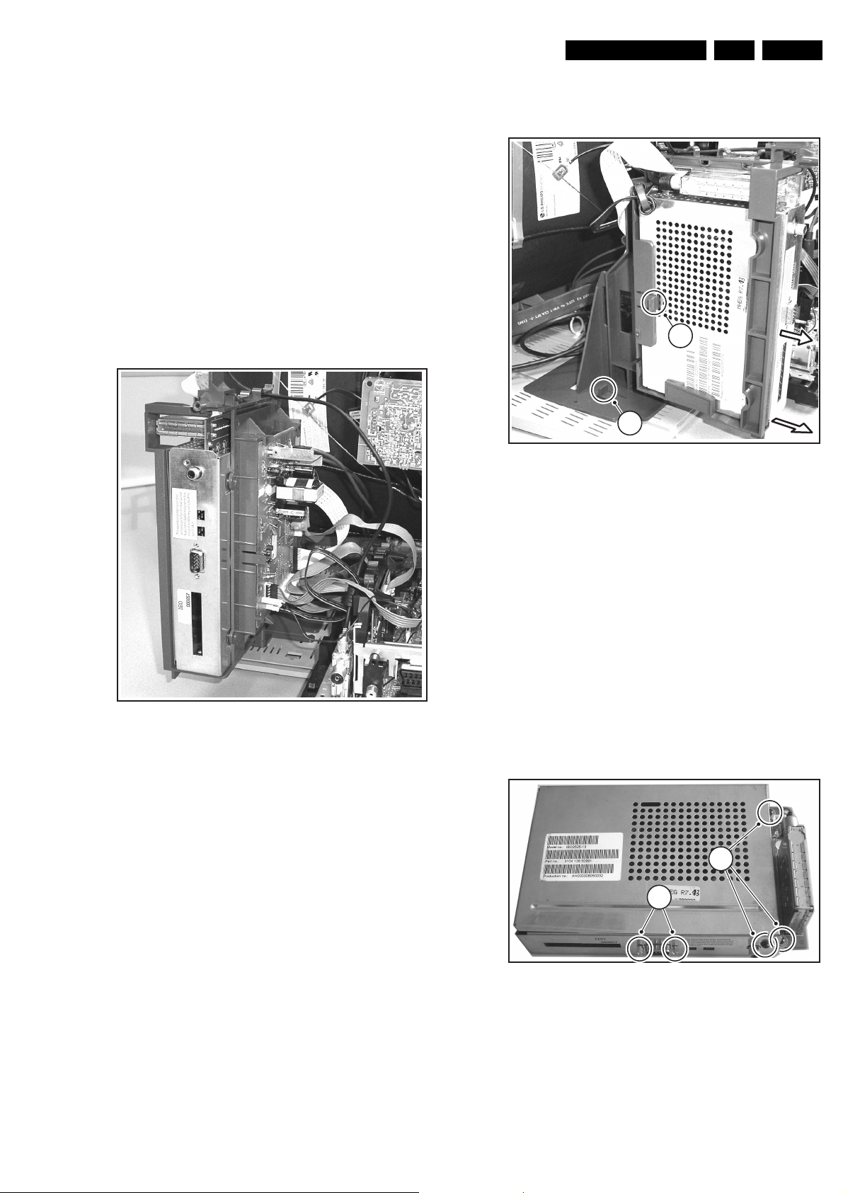
4. Mechanical Instructions
Index of this chapter:
1. IBO+ Assy Removal
2. IBO+ Module Removal
3. IBO+ panel Removal
4. Power Supply Panel Removal
5. Re-Assembly
Notes:
• Only the digital module disassembly is described. For other
disassembly instructions, see the Service manual A10E
3122 785 10430.
• Figures can deviate slightly from the actual situation, due
to different set executions.
Mechanical Instructions
EN 15A10E BB 4.
4.1 IBO+ Assy Removal
Figure 4-1 IBO+ assy
1. Make sure all power-, audio-, video- and coax- cables are
unplugged from the set.
2. Before you can access the IBO+ assy, remove the rear
cover (see the Service manual A10E 3122 785 10430).
3. Pull up the clip (1) at the left side of the IBO+ bracket and,
at the same time, pull the bracket forward until it is
released.
CL 36532080_066.eps
271103
2
1
Figure 4-2 IBO+ bracket
4.2 IBO+ Module Removal
1. Disconnect all IBO+ module connectors.
2. Remove the two mounting screws at right side of the IBO+
module.
3. Unlock the clip (2) at the left side of the bracket and pull out
the IBO+ module (see figure “IBO+ bracket”)
4.3 IBO+ Panel Removal
1. Unscrew the shield mounting screws (1) and remove the
shield.
2. Use a 5 mm socket screwdriver to remove both connector
distance bolts (2) from the Sub-D connector.
3. Unscrew the IBO+ panel mounting screws and take out the
IBO+ panel.
1
CL 36532080_067.eps
271103
2
Figure 4-3 IBO+ panel schield
Important: Viper chip heat sink.
• Before you de-solder the viper chip PNX8525 from the
board, the heat sink must be removed from the chip. Use a
pair of pliers to take off the heat sink by means of a twistand pull movement (see figure), before you de-solder the
viper chip PNX8525 from the board. Store the heat sink on a safe place, adhesive side up!
CL 36532080_068.eps
271103
Page 16
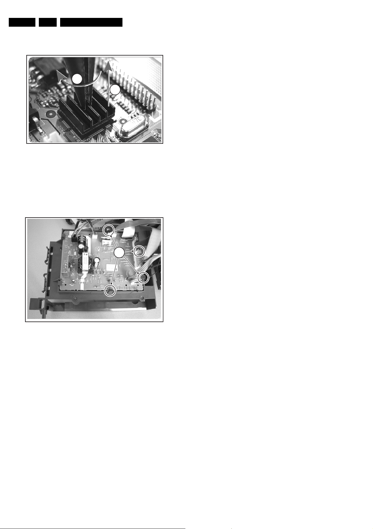
EN 16 A10E BB4.
• Place the self adhesive heat sink back in place after the
chip exchange action has been finished.
1
2
Mechanical Instructions
Figure 4-4 Heat sink removal
4.4 Power Supply Panel Removal
1. Unplug all cables from the Power supply panel.
2. Unlock the four securing clips (1), which hold the panel in
place, and take out the Power supply panel.
1
CL 36532080_082.eps
CL 36532080_069.eps
091203
271103
Figure 4-5 Power supply panel
4.5 Re-Assembly
To re-assemble the whole set, do all processes in reverse
order.
Page 17
Service Modes, Error Codes, and Fault Finding
5. Service Modes, Error Codes, and Fault Finding
EN 17A10E BB 5.
Index of this chapter:
1. Test points
2. Service Modes
3. ComPair
4. Error Codes
5. The Blinking LED Procedure
6. Protections
7. Troubleshooting Tips
8. Flash-card Handling for SW Downloading
5.1 Test Points
The chassis is equipped with test points printed on the circuit
board assemblies. These test points refer to the functional
blocks:
Table 5-1 Test point overview
Test point Cuircuit Diagram
A1-A2-A3-..... Audio processing A6, C6
C1-C2-C3-..... Control C8
F1-F2-F3-..... Frame drive and output A3
I1-I2-I3-..... Tuner & IF A4, C1
I5xx-I6xx-I7xx-..... IBO+ K, S
L1-L2-L3-.... Line drive and output A2
P1-P2-P3-..... Power supply A1
S1-S2-S3-..... Synchronisation C1
V1-V2-V3-..... Video processing B, C2, C3
The numbering is in a logical sequence for diagnostics. Always
start diagnosing within a functional block in the sequence of the
relevant test points for that block.
Perform measurements under the following conditions:
• Service Default Mode.
• Video: colour bar signal.
• Audio: 3 kHz left, 1 kHz right.
– Child/parental lock,
– Blue mute,
– Hotel/hospitality mode
– Auto switch-off (when no ‘IDENT’ video signal is
received for 15 minutes),
– Skip / blank of non-favourite presets / channels,
– Auto store of personal presets,
– Auto user menu time-out.
How to enter SDM
Use one of the following methods:
• Use a standard customer RC-transmitter and key in the
code ‘062596’ directly followed by the MENU button, or
• Short wires 9261 and 9262 on the mono carrier, and apply
Mains power. Then press the power button (remove the
short after start-up).
Caution: Entering SDM by shorten wires 9261 and 9262
will override the +5V-protection. Do this only for a short
period. When doing this, the service-technician must know
exactly what he is doing, as it could lead to damaging the
set (in case of SW protections (error 1-4) the set will
shutdown after 15 s).
• Or, via ComPair.
After entering SDM, the following screen is visible, with SDM at
the upper right side for recognition.
SDM Menu
HRS: 0001 SWID: A10 EU1-2.7
ERR: 0 0 0 0 0 0 0
SDM
PICTURE BRIGHTNESS
+
SDM
SOUND COLOURNESS
MENU
FEATURES CONTRAST
INSTALL SHARPNESS
STORE
CL 06532012_008.eps
SDM
030200
5.2 Service Modes
Service Default Mode (SDM) and Service Alignment Mode
(SAM) offer several features for the service technician, while
the Customer Service Menu (CSM) is used for communication
between dealer and customer.
There is also the option of using ComPair, a hardware interface
between a computer (see requirements) and the TV chassis. It
offers the ability of structured trouble shooting, error code
reading, and software version readout.
Minimum requirements: a 486 processor, Windows 3.1 and a
CD-ROM drive. A Pentium Processor and Windows 95/98 are
also acceptable (see also paragraph “ComPair”).
5.2.1 Service Default Mode (SDM)
Purpose
To create a predefined setting to get the same measurement
results as given in this manual.
To override SW protections.
To start the blinking LED procedure.
Specifications
• Tuning frequency: 475.25 MHz.
• Colour system: PAL-BG.
• All picture settings at 50 % (brightness, colour contrast,
hue).
• Bass, treble and balance at 50 %; volume at 25 %.
• All service-unfriendly modes (if present) are disabled, like:
– (Sleep) timer,
Figure 5-1 Example of SDM menu
Special functions in SDM
• Access to normal user menu: Pressing the MENU button
on the remote control switches between the SDM and the
normal user menus (with the SDM mode still active in the
background)
• Channel search: Pressing the “P+” button of the remote
control starts a tuning search. Search is indicated by a
blinking LED (this stops when a transmitter is found; the
transmitter is stored on the highest channel number,
typically this is 99 and the TV switches to this preset)
• Error buffer: Pressing the OSD button [i+] of the remote
control shows/hides the error buffer. OSD can be hidden to
prevent interference with oscillogram measurements.
• Access to SAM: By pressing the “VOLUME +” and
“VOLUME -“ buttons on the local keyboard simultaneously
the set switches from SDM to SAM.
How to navigate
Use one of the following methods:
• When you press the MENU button on the remote control,
the set will switch between the SDM and the normal user
menu (with the SDM mode still active in the background).
Return to the SDM screen with the OSD / STATUS button.
• When you press the OSD / STATUS button on the remote
control, the menu will show or hide the error buffer. This
feature is available to prevent interference during
waveform measurements.
Page 18
EN 18 A10E BB5.
Service Modes, Error Codes, and Fault Finding
• On the TV, press and hold the 'VOLUME down' and press
the 'CHANNEL down' for a few seconds, to switch from
SDM to SAM and reverse.
How to exit
Switch the set to STANDBY by pressing the power button on
the remote control transmitter (if you switch the set “off” by
removing the Mains power, the set will return in SDM when
Mains power is re-applied). The error buffer is cleared.
5.2.2 Service Alignment Mode (SAM)
Purpose
• To perform alignments.
• To change option settings.
• To display / clear the error code buffer.
• Specifications
• Operation hours counter.
• Software version.
• Option settings.
• Error buffer reading and erasing.
• Software alignments.
How to enter
Use one of the following methods:
• Use a standard customer RC-transmitter and key in the
code ‘062596’ directly followed by the OSD / STATUS
button [i+], or
• By pressing the “VOLUME +” and “VOLUME -” key on the
local keyboard simultaneously, when the set is in SDM, or
• Via ComPair.
The following screen is visible, with SAM at the upper right side
for recognition.
SAM Menu
PICTURE BRIGHTNESS
SOUND COLOURNESS
FEATURES CONTRAST
INSTALL SHARPNESS
1
HRS: 0038 SWID: A10EMH-1.0-2.7
ERR: 0 0 0 0 0 0 0
OPT: 254 100 128 0 0 0 0 0
CLEAR ERRORS
OPTIONS
AKB OFF
VSD OFF
TUNER
WHITE TONE
GEOMETRY
SUPER WIDE
SOUND
SMART SETTING
5
STORE
MENU
SAM
2 3 4
SAM
MENU
MENU
MENU
MENU
MENU
MENU
NPRG
WSSB
SYSTEM
OB1
OB2
TUNER
IF-PLL OFFSET
AFC WINDOW
AGC
AFA
AFB
NORMAL RED
MENU
VER-AMPL
VER-AMPL
SOUND
NIC-FMAM
PS-FM
PS-NIC-BGDK
PS-NIC-I
RICH
RICH BGT
RICH COL
RICH CON
RICH SHP
RICH HUE
Figure 5-2 Example of SAM menu
1. Operation hours timer (hexadecimal)
2. Software identification of the main micro controller
(A10BBC-X.Y)
• A10 is the chassis name
• BBC is 2 letter and 1 digit combination to indicate the
software type and the supported languages:
• X = (main version number)
SAM
SAM
KHZ(100/250)
SAM
SAM
SAM
SAM
SAM
CL 36532080_080.eps
031203
• Y = (subversion number)
3. Error buffer (7 errors possible)
4. Option bytes (8 codes possible), summary of options are
explained below
5. CLEAR ERRORS. Erasing the contents of the error buffer.
Select the CLEAR ERRORS menu item and press the
MENU RIGHT key. The content of the error buffer is
cleared.
The functionality of the OPTIONS and ALIGNMENTS
(TUNER, WHITE TONE, GEOMETRY, SOUND and SMART
SETTING) sub menus is described in chapter “Alignments”.
How to navigate
Use one of the following methods:
• In SAM, select menu items with the CURSOR UP/DOWN
key on the remote control transmitter. The selected item
will be highlighted. When not all menu items fit on the
screen, move the CURSOR UP/DOWN key to display the
next / previous menu items.
• With the CURSOR LEFT/RIGHT keys, it is possible to:
– (De)activate the selected menu item.
– Change the value of the selected menu item.
– Activate the selected submenu.
• When you press the MENU button twice, the set will switch
to the normal user menus (with the SAM mode still active
in the background). To return to the SAM menu press the
OSD / STATUS button [i+].
• When you press the MENU key in a submenu, you will
return to the previous menu.
How to exit
Switch the set to STANDBY by pressing the power button on
the remote control (if you switch the set “off” by removing the
Mains power, the set will return in SAM when Mains power is
re-applied). The error buffer is not cleared.
5.2.3 Customer Service Mode (CSM)
Purpose
When a customer is having problems with his TV-set, he can
call his dealer. The service technician can than ask the
customer to activate the CSM, in order to identify the status of
the set. Now, the service technician can judge the severness of
the complaint. In many cases, he can advise the customer how
to solve the problem, or he can decide if it is necessary to visit
the customer.
The CSM is a read only mode; therefore, modifications in this
mode are not possible.
How to enter
The CSM will be turned on after pressing the MUTE key on the
remote control transmitter and any of the control buttons on the
TV for at least 4 seconds simultaneously. This activation only
works if there is no menu on the screen.
After switching ON the Customer Service Mode, the following
screen will appear:
CSM Menu
1 HRS: 0005 SWID: A10EU1-2.7
2 CODES: 0 0 0 0 0 0 0
3 OPT: 254 100 128 0 0 0 0 0
4 SYSTEM: EUROPE 11 SOUND: MONO
5 NO SIGNAL 12 VOLUME:
6 13 BALANCE: +/7 14 HUE: +/8 15 COLOUR:
9 16 BRIGHTNESS:
10 SOURCE: 1 17 CONTRAST:
Figure 5-3 Example of CSM Menu
CSM
CL 06532012_010.eps
070200
Page 19

Service Modes, Error Codes, and Fault Finding
EN 19A10E BB 5.
1. HRS and SWID. HRS: Hexadecimal counter of operating
hours (Standby hours are not counted as operating hours).
SWID: Software identification of the main micro controller.
See paragraph 5.2. Details on available software versions
can be found in the chapter “Software Survey” of the
publication “Product Survey - Colour Television”.
2. CODES. Error code buffer (see paragraph 5.3). Displays
the last 7 errors of the error code buffer.
3. OPT. Option bytes. Software and hardware functionality of
this chassis is controlled by option bits. An option byte or
option number represents 8 of those bits. Each option
number is displayed as a decimal number between 0 and
255. The set may not work correctly when an incorrect
option code is set. See chapter 8 for more information on
correct option settings
4. SYSTEM. Indicates which colour and sound system is
installed for this preset. Complaints that may be caused by
an incorrect system setting: no colours, colours not correct,
unstable picture, or noise in picture. To change the system
setting of a preset:
– Press the MENU button on the remote control
– Select the INSTALL sub menu
– Select the MANUAL STORE sub menu
– Select and change the SYSTEM setting until picture
and sound are correct
– Select the STORE menu item
5. NO SIGNAL. Indicates that the set is not receiving an
“ident” signal on the selected source.
– No or bad antenna signal; connect a proper antenna
signal
– Antenna not connected; connect the antenna
– No channel / preset is stored at this program number;
go to the INSTALL menu and store a proper channel at
this program number
– The tuner is faulty (in this case the CODES line will
contain number 13); check the tuner and replace/repair
if necessary
– Note: On some models, BLUE MUTE is displayed (if
the BM option is ON) when no signal is received.
6. TIMER ON. Indicates that the on/off timer is running.
Complaints that may be caused by the activation of the
sleep timer. Without using the remote control of the local
keyboard, the set is switching on from standby, or to a
different channel. To switch the activation timer “off”:
– Select “TIMER” in the “FEATURE” menu
– Select “ACTIVATE’ in the “TIMER” menu
– Set to “OFF” with the left/right cursor keys
7. CHANNEL BLOCKED. Indicates that all channels are
locked except the selected channel. Complaints that may
be caused by locked channels are: TV cannot be switched
on from standby with the local keyboard buttons, or “P+”
and “P-“ buttons on local keyboard do not function. To
disable the LOCK feature:
– Select ”FEATURE” menu (with the Remote Control)
– Select “LOCK” (with the RC)
– Set to “OFF”
8. NOT PREFERED. Indicates that at least one channel is
deleted as a preferred channel (by default, all channels are
skipped. Note that “SKIPPED” will always be displayed in
CSM unless no channels are skipped. A channel can be
added as a selected channel to the list of preferred
channels:
– Select “INSTALL” menu
– Select “CHANNEL EDIT”
– Select “ADD/DELETE”
– Set to “ADD” with the left/right cursor keys
9. HOTEL MODE. Indicates that the Hotel mode has been
activated.
10. SOURCE. Indicates which SOURCE is installed for this
preset: EXT1, SVHS2, EXT2, Tuner.
11. SOUND. Indicates which sound mode is installed for this
preset: Mono, NICAM, Stereo, L1, L2, SAP, Virtual or
Digital.
12. VOLUME. Value indicates level at entry CSM.
13. BALANCE. Value indicates level at entry CSM.
14. HUE. Value indicates level at entry CSM.
15. COLOR. Value indicates level at entry CSM.
16. BRIGHTNESS. Value indicates level at entry CSM.
17. CONTRAST. Value indicates level at entry CSM.
How to exit
Use one of the following methods:
• After you press ‘any’ key of the remote control transmitter
with exception of the CHANNEL and VOLUME keys.
• After you switch "off" the TV set with the Mains power
switch.
5.3 ComPair
5.3.1 Introduction
ComPair (Computer Aided Repair) is a service tool for Philips
Consumer Electronics products. ComPair is a further
development on the European DST (service remote control),
which allows faster and more accurate diagnostics. ComPair
has three big advantages:
ComPair helps you to quickly get an understanding on how to
repair the chassis in a short time by guiding you systematically
through the repair procedures.
ComPair allows very detailed diagnostics (on I2C level) and is
therefore capable of accurately indicating problem areas. You
do not have to know anything about I2C commands yourself
because ComPair takes care of this.
ComPair speeds up the repair time since it can automatically
communicate with the chassis (when the microprocessor is
working) and all repair information is directly available. When
ComPair is installed together with the SearchMan electronic
manual of the defective chassis, schematics and PWBs are
only a mouse click away.
5.3.2 Specifications
ComPair consists of a Windows based faultfinding program
and an interface box between PC and the (defective) product.
The ComPair interface box is connected to the PC via a serial
or RS232 cable.
In this chassis, the ComPair interface box and the TV
communicate via a bi-directional service cable via the service
connector.
The ComPair faultfinding program is able to determine the
problem of the defective television. ComPair can gather
diagnostic information in two ways:
• Automatic (by communication with the television):
ComPair can automatically read out the contents of the
entire error buffer. Diagnosis is done on I2C level. ComPair
can access the I2C bus of the television. ComPair can
send and receive I2C commands to the micro controller of
the television. In this way, it is possible for ComPair to
communicate (read and write) to devices on the I2C
busses of the TV-set.
• Manually (by asking questions to you): Automatic
diagnosis is only possible if the micro controller of the
television is working correctly and only to a certain extend.
When this is not the case, ComPair will guide you through
the faultfinding tree by asking you questions (e.g. Does the
screen give a picture? Click on the correct answer: YES /
NO) and showing you examples (e.g. Measure test-point I7
and click on the correct waveform you see on the
oscilloscope). You can answer by clicking on a link (e.g.
text or a waveform picture) that will bring you to the next
step in the faultfinding process.
By a combination of automatic diagnostics and an interactive
question / answer procedure, ComPair will enable you to find
most problems in a fast and effective way.
Beside fault finding, ComPair provides some additional
features like:
Page 20
EN 20 A10E BB5.
Service Modes, Error Codes, and Fault Finding
• Up- or downloading of pre-sets.
• Managing of pre-set lists.
• Emulation of the Dealer Service Tool (DST).
• If both ComPair and SearchMan (Electronic Service
Manual) are installed, all the schematics and the PWBs of
the set are available by clicking on the appropriate
hyperlink.
Example: Measure the DC-voltage on capacitor C2568
(Schematic/Panel) at the Mono-carrier.
– Click on the 'Panel' hyperlink to automatically show the
PWB with a highlighted capacitor C2568.
– Click on the 'Schematic' hyperlink to automatically
show the position of the highlighted capacitor.
5.3.3 How To Connect
1. First, install the ComPair Browser software (see the Quick
Reference Card for installation instructions).
2. Connect the RS232 interface cable between a free serial
(COM) port of your PC and the PC connector (marked with
'PC') of the ComPair interface.
3. Connect the mains adapter to the supply connector
(marked with 'POWER 9V DC') of the ComPair interface.
4. Switch the ComPair interface “off”.
5. Switch the television set “off” with the mains switch.
6. Connect the ComPair interface cable between the
connector on the rear side of the ComPair interface
(marked with 'I2C') and the ComPair connector at the rear
side of the TV (situated just below the main aerial input).
7. Plug the mains adapter in a mains outlet, and switch the
interface “on”. The green and red LEDs light up together.
The red LED extinguishes after approx. 1 second while the
green LED remains lit.
8. Start the ComPair program and read the 'Introduction'
chapter.
5.3.4 How To Order
ComPair order codes:
• Starter kit ComPair32/SearchMan32 software and
ComPair interface (excl. transformer): 3122 785 90450.
• ComPair interface (excluding transformer): 4822 727
21631.
• Starter kit ComPair32 software (registration version): 3122
785 60040.
• Starter kit SearchMan32 software: 3122 785 60050.
• ComPair32 CD (update): 3122 785 60070 (year 2002,
3122 785 60110 (year 2003).
• SearchMan32 CD (update): 3122 785 60080 (year 2002),
3122 785 60120 (year 2003).
• ComPair interface cable: 3122 785 90004.
• ComPair firmware upgrade IC: 3122 785 90510 (only for
sets with software upgrade facilities).
• Transformer (non-UK): 4822 727 21632.
• Transformer UK: 4822 727 21633.
Note: If you encounter any problems, contact your local
support desk.
5.4 Errors
5.4.1 Error code buffer
The error code buffer contains all detected errors since the last
time the buffer was erased. The buffer is written from left to
right. When an error occurs that is not yet in the error code
buffer, it is written at the left side and all other errors shift one
position to the right.
5.4.2 How to Read the Error Buffer
EXTERNAL 2
L
R
AUDIO EXTERNAL 1
SERVICE
CONNECTOR
PC VCR I2CPower
9V DC
Figure 5-4 ComPair Interface connection
CL96532156_029.eps
190600
Use one of the following methods:
• On screen via the SAM (only if you have a picture).
Examples:
– ERROR: 0 0 0 0 0 : No errors detected
– ERROR: 6 0 0 0 0 : Error code 6 is the last and only
detected error
– ERROR: 9 6 0 0 0 : Error code 6 was first detected and
error code 9 is the last detected (newest) error
• Via the blinking LED procedure (when you have no
picture). See next paragraph.
• Via ComPair.
5.4.3 How to Clear the Error Buffer
The error code buffer is cleared in the following cases:
• By activation of the CLEAR command in the SAM menu:
• When you exit SDM / SAM with the STANDBY command
on the remote control (when leaving SDM / SAM, by
disconnecting the set from Mains power, the error buffer is
not reset).
• When you transmit the command DIAGNOSE-99-OK with
ComPair.
• If the content of the error buffer has not changed for 50
hours, it resets automatically.
5.4.4 Error Codes
In case of non-intermittent faults, clear the error buffer before
you begin the repair. These to ensure that old error codes are
no longer present.
If possible, check the entire contents of the error buffer. In
some situations, an error code is only the result of another error
code and not the actual cause (e.g., a fault in the protection
detection circuitry can also lead to a protection).
Page 21
Service Modes, Error Codes, and Fault Finding
EN 21A10E BB 5.
Table 5-2 Error code overview
Error Error description Possible defective components
No error detected
1 X-ray protection/ EW and/or
High beam protection active
2 Vertical protection Vertical circuit is defective
3 Reserved
4 5V protection active +5V supply line is low or short circuit
5 Reserved
6 General I2C bus error I2C bus s/c or o/c on uP
7 BC-loop not stabilised RGB amplifiers, RGB guns or RGB
8 BOCMA I2C error IC7301 - TDA8885
9 BOCMA 8V supply failure IC7301 and R3331
10 NVM I2C error IC7066 - M24C32
11 NVM identification failure IC7066 - M24C32
12 Microprocessor internal RAM
test failure
13 Main Tuner I2C error IC1225 - UV13xx / TEDE9
14 Sound processor I2C error IC7651 - MSP3415 / 3451
15 SRAM I2C error IC7070 - UPDxxxx
24 IO expander IC (on Dig. Interf.
panel)
25 IBO+ microprocessor (Viper) IC7100 - PNX8525
LOT, Line deflection circuit,
EW-circuit or CRT amplifier circuit,
picture tube or +200V missing
driving signals of BOCMA
IC7064 - SAA5667
IC7008 - PCF8574
Error 0 = No error
Error 1 = X-ray protection, E/W protection and/or IBeam.
The set is switched to protection; error code 1 is placed in the
error buffer; the LED will blink 1 time (repeatedly). If this
happens, isolate each circuit to determine the cause. These
circuits are:
• X-Ray protection (PROTN). If this protection is active, the
most likely cause is the LOT. Detection via pin 3 of the
BOCMA (item 7301).
• EW protection (PROT-UP). If this protection is active, the
causes could be one of the following;
– Bad contacts of: horizontal deflection coil, linearity coil
5417, S-correction capacitor 2418/2419, flyback
capacitor 2414/2416, or line output stage.
– Short circuit of: flyback diode 6414, EW transformer
(bridge coil) 5478/5479 or 5474/5475/5476 (version
dependent), or EW driver 7470.
• High beam current protection (IBEAM). As the name
implies, the cause of this protection is a too high beam
current (bright screen with flyback lines). Check whether
the +200 V supplies to the CRT panel is present. If the
voltage is present, the most like cause is the CRT panel or
the picture tube. Disconnect the CRT panel to determine
the cause. If the +200 V voltage is not present, check
R3840 at CRT-panel and R3445 / D6445 at main panel.
Error 2 = Vertical protection (VFB). If this protection is active,
the cause could be one of the following (most likely in the
vertical output stage):
• 7501 is faulty.
• Poor contact or open circuit of deflection coil.
• +13 V-VERT and/or -13 V not present.
Error 3 = Reserved
Error 4 = +5 V protection. If the 5 V protection is active, the set
is switched to protection, error code 4 is placed in the error
buffer, and the LED will blink 4 times (repeatedly).
A 5 V failure can cause a drop in the 5 V supply output,
resulting in an undefined behaviour of the set. Therefore, all
I2C devices connected to the 5 V supply are constantly
monitored. When none of these devices respond to the micro
controller for a prolonged time, the micro controller assumes
that there is a failure in the 5 V supply.
By starting up the set with the service jumpers shorted, the 5 V
protection is disabled and it is easier to determine the cause.
+5 V protection will be activated when these I2C devices fail
(no I2C communication):
• Main Tuner 1125 on main panel.
• ITT sound processor MSP34xx (7064) on the SSB.
The following tips are useful to isolate the problem area after
overriding the +5V protection. Determine whether:
• The +5 V source is working properly; isolate coil 5430 and
jumper 9044 and measure the +5V
• ITT sound processor circuit is loading the +5 V; isolate coil
5430.
• The tuner is loading the +5 V source; isolate jumper 9044.
• Main tuner circuit is loading the +5 V source; isolate coil
5261.
Caution: Overriding the 5 V protection when there is a 5 V
failure can increase the temperature in the set and may cause
permanent damage to components. Do not override the 5 V
protection for a prolonged time.
Error 5 = Reserved.
Error 6 = General I2C error. This will occur in the following
cases:
• SCL or SDA is shorted to ground.
• SCL is shorted to SDA.
• SDA or SCL connection at the micro controller is open
circuit.
Error 7 = BC-loop not stabilised (BCF = 1) Black current loop
instability protection. The possible cause could be a defect in
one or more of the RGB amplifiers, RGB guns or RGB driving
signals.
Error 8 = BOCMA IC TDA888xx I2C communication failure.
BOCMA (item 7301 on SSB) is corrupted, or the I2C line to the
BOCMA is low, or no supply voltage present at pin 14 and/or
pin 60 (3V3).
Error 9 = BOCMA IC TDA888xx 8 V failure (SUP bit). No
supply voltage at pin 53. Check NFR 3331 and coil 5333.
Error 10 = NVM I2C error. NV memory (item 7066) does not
respond to the micro controller.
Error 11 = Micro controller / NV Memory identification error.
During the last start-up, the NVM and the micro controller did
not recognize each other (e.g. one of them was replaced or the
NVM memory has been changed/adapted or lost); therefore,
the NVM was loaded with default values.
Error 12 = Microprocessor (item 7064) internal RAM test
failure.
Error 13 = Main Tuner I2C failure UV13xx. Tuner (item 1225)
is corrupted, or the I2C line to the Tuner is low, or nosupply
voltage at pin 9, pin 6 or 7 of the tuner.
Error 14 = Sound processor I2C error (MSP34xx). Sound
controller MSP3400 or MSP3410 does not respond to the
micro controller.
Error 15 = SRAM IC uPD431000A-B test failure (item 7070).
Error 24 = IO expander IC (IC7008 - PCF8574 on Dig. Interf.
panel) I2C communication failure.
Error 25 = IBO+ microprocessor (IC7100 - PNX8525) I2C
communication failure.
Note: Error codes 1, 2, and 4 are protection codes and in this
case, supply of some circuits will be switched “off”. In addition,
in protection, the LED will blink the number of times equivalent
to the most recent error code.
Page 22

EN 22 A10E BB5.
Service Modes, Error Codes, and Fault Finding
5.5 The Blinking LED Procedure
Via this procedure, you can make the contents of the error
buffer visible via the front LED. This is especially useful when
there is no picture.
When the SDM is entered, the LED will blink the contents of the
error-buffer.
Error-codes ≥ 10 are shown as follows:
• A long blink of 750 ms (which is an indication of the decimal
digit),
• A pause of 1.5 s,
• n short blinks (n = 1 - 9),
• When all the error-codes are displayed, the sequence
finishes with a LED blink of 3 s,
• The sequence starts again.
Example of error buffer: 12 9 6 0 0
After entering SDM:
• 1 long blink of 750 ms followed by a pause of 1.5 s,
• 2 short blinks followed by a pause of 3 s,
• 9 short blinks followed by a pause of 3 s,
• 6 short blinks followed by a pause of 3 s,
• 1 long blink of 3 s to finish the sequence,
• The sequence starts again.
5.6 Protections
If a fault situation is detected an error code will be generated
and if necessary, the set will be put in the protection mode.
Blinking of the red LED at a frequency of 3 Hz indicates the
protection mode. In some error cases, the microprocessor
does not put the set in the protection mode. The error codes of
the error buffer can be read via the service menu (SAM), the
blinking LED procedure or via ComPair. The DST diagnose
functionality will force the set into the Service-standby, which is
similar to the usual standby mode, however the microprocessor
has to remain in normal operation completely.
To get a quick diagnosis the chassis has three service modes
implemented:
• The Customer Service Mode (CSM).
• The Service Default Mode (SDM). Start-up of the set in a
predefined way.
• The Service Alignment Mode (SAM). Adjustment of the set
via a menu and with the help of test patterns.
See for a detailed description: Chapter 9 paragraphs
“Deflection” and “Power Supply” of the A10E Service manual.
5.7 Troubleshooting Tips
In this paragraph, some troubleshooting tips for the deflection
and power supply circuitry are described.
position numbers 9409 (in this case the EW protection is
disabled). If the basic deflection is working (picture is
parabolic distorted), then the fault is located in the EW
circuit/panel. If there is no hor. deflection, the fault is
present in the basic deflection circuitry.
• Also, take note of protection circuits in the line output
stage. If any of these circuits are activated, the set will shut
down. Depending on protections, the LED will blink
according to the fault defined. In order to determine which
protection circuit is active, isolation of circuits is necessary.
These protection circuits are:
– High beam protection: See error “1”.
– X-ray protection: See error “1”.
• If the high beam protection or the X-ray protection is active,
it will switch the set to protection and the SDM is activated.
The service LED blinks repetitively 1 time. If this happen,
isolate each circuit to determine the cause.
5.7.2 Power Supply
To trouble shoot the A10 SMPS, first check the +5 V_STBY
voltage on IC7968, pin 3 / 4. If this voltage is not present, check
fuse 1961 and D6961.
If 1906 or D6917 is not open circuit, the problem might be
caused on the primary side of the switching supply. Check the
output of the bridge diodes at the cathode side of D6912/D6913
or D6915-pin 1 for approximately 300 V_dc. If this voltage is
missing, check the bridge diodes and the fuse. If fuse F1900 is
found open, check IC7921 (circuit A1) between pins 3 and 2 to
make sure that there is no short circuit present.
If the 300 V_dc is present on pin 3 of IC7902, check for a startup voltage of 16 V on pin 4 of IC7921. If this start-up voltage is
not present, check if R3914 is open (a short circuit between pin
4 and 5 will also cause this problem). It is necessary to have a
feedback signal from the hot secondary side of switch mode
transformer T5912 at pin 8 and pin 9 for the power supply to
oscillate. If this start-up voltage is present on pin 4 of IC7902
and the supply is not oscillating, check R3929 and D6929.
The A10 power supply has been designed with Over Voltage
Protection (OVP). To determine whether OVP is active, check
whether V_BAT (141 V) is present at IC7971 pin 1. If not, check
the components D6938, C2939 and C2940 and L5941. If these
components are o.k., then check voltage at pin 3 of IC 7942.
If this voltage is not present check fuse 1941 and fuse 1942.
Replace if necessary.
If the dc-voltage is present at pin 3, replace opto-coupler 7929.
Another way to confirm whether OVP is active is to measure
the voltage with an oscilloscope at IC7902 pin 4. If the voltage
is fluctuating between 11-14 V, then check the components as
described in the above mentioned paragraph.
5.7.3 Other Problems (related to CSM)
Picture problems
5.7.1 Deflection Circuit
• Measure if the V_BAT (140 V) is present across 2939/2940
(A1 POWER SUPPLY). If the voltage is not present,
disconnect jumper 9936 and 9937 (see A1 Power Supply).
The whole Line Deflection stage is now disconnected. If the
voltage is present, then the problem might be caused by
the deflection circuit. Possibilities:
– Transistor 7410 is defective.
Note: If the C and E of 7410 are shorted, hick-up noise
can be heard from the power supply circuit
– The driver circuit around transistor 7481 is faulty
– No horizontal drive signal coming from the BOCMA IC
7301 pin 56 on the SSB
• To determine whether the fault is present in the line
deflection circuit (A2 LINE DEFLECTION) or in the EW
circuit/panel (screen size above 21”), insert jumper into
TV switched off or changed channel without any user action
Set switches off after “TV SWITCHING OFF” was displayed:
“Auto standby” switched the set off because:
• There was no ident signal for more than 15 minutes
• There was no remote control signal received or local key
pressed for > 2 hours
See chapter “Alignments” for a description on the options to
enable/disable auto standby
Picture too dark or too bright
• Press “Smart Picture” button on the remote control. In case
the picture improves, increase / decrease the brightness
value or increase / decrease the contrast value. The new
“Personal Preference” value is automatically stored after 3
minutes
• After switching on the Customer Service Mode, the picture
is OK. Increase / decrease the brightness value or increase
Page 23

Service Modes, Error Codes, and Fault Finding
EN 23A10E BB 5.
/ decrease the contrast value. The new “Personal
Preference” value is automatically stored after 3 minutes
White line around picture elements and text
• Press “Smart Picture” button on the remote control. In case
the picture improves, decrease the sharpness value. The
new “Personal Preference” value is automatically stored
after 3 minutes
• After switching on the Customer Service Mode, the picture
is OK. Decrease the sharpness value. The new “Personal
Preference” value is automatically stored after 3 minutes
Snowy picture
• Check the “NOT TUNED” section of the Customer Service
Mode screen
Snowy picture and/or unstable picture
• A scrambled or decoded signal is received
Black and white picture
• Press “Smart Picture” button on the remote control. In case
picture improves, increase the colour value. The new
“Personal Preference” value is automatically stored after 3
minutes
• After switching on the Customer Service Mode, the picture
is OK. Increase the colour value. The new “Personal
Preference” value is automatically stored after 3 minutes
Menu text not sharp enough
• Press “Smart Picture” button on the remote control. In case
the picture improves, decrease the contrast value. The new
“Personal Preference” value is automatically stored after 3
minutes
• After switching on the Customer Service Mode, the picture
is OK. Decrease the contrast value. The new “Personal
Preference” value is automatically stored after 3 minutes
Sound Problems
No sound or sound too loud (after channel change / switching on)
• After switching on the Customer Service Mode, the volume
is OK. Increase / decrease the volume level. The new
“Personal Preference” value is automatically stored after 3
minutes.
5.8 Flash-card Handling For SW Downloading
5.8.1 General
You must NOT:
• Use Sony writers.
• Format the cards.
• Use a flash-card from Apacer.
• Use flash-cards > 256 MB
You must:
• Use USB writers. Use a PCMCIA card adapter and a
laptop.
• Use brands Kingston and Sandisk for flash-cards.
• Use flash-card of sizes of 32 MB, 64 MB, 128 MB and 256
MB.
• Use a DOS box or Windows Explorer to copy the two
images (FCL.IMG and IBOP.IMG) to the flash-card. Those
two files form a pair. Always copy both images (from the
same delivery!). Make very sure that the images, which
you are trying to install, are made for that particular board
model and that particular board version. In addition, the
Software version or model should differ from the version
or model, which is already on the board. If it does not differ,
no download will take place (unless the software on the
board was faulty).
• In order to make sure that the writing indeed has finished,
you must do the following before removing the card:
Software “Eject” or “Disconnect” the driver (should be a
command of your flash-card writer, which you can see
when you right-click on the flash-card drive from the
explorer.) If you forget this, not all data is flashed to the
card, resulting in incomplete files on the flash-card.
5.8.2 Solving problems
In case of any troubles, first do the following to check whether
the copy was good:
1. Remove the flash-card (so that the cache memory is
cleared).
2. After 10 seconds, re-insert the flash-card.
3. Open a DOS box and type "fc /b <image on card> <image
on harddisk>".
This command does compare the copy of the image with
the original, which should not have any differences.
You put a flash-card in and the system does nothing. The
flash-card loader is copying the image to flash. This can take
up to 1.5 minutes (for large images).
Whenever you reset the board, an application is launched.
• Press the flash-card firmly into it's slot; if it is not inserted
properly the available application will launch
• Check (with an PC / laptop) that the flash-card contains
both a FCL.IMG and a IBOP.IMG.
• Always copy both images as the FCL.IMG and the
IBOP.IMG form a pair.
The flash-card images do not download (board keeps on
resetting or IBL is launched, or another application is launched
from NAND-flash).
• Make sure the Software Version you try to download is
different from the one in the box.
• Make sure the Hardware Version is set correctly. L0, L1,
and L2 boards all use different flash-card images.
• Make sure the contents of the flash-card are readable
(check with NT); try another flash-card and another flashcard writer on another PC to be 100% sure. Do not format
the flash-card.
Flashing of NOR-image does not work. Remove the stream
server (!).
Flashing of NAND-flash does not work. Check the size of the
IBOP.IMG image. It should not exceed +/- 15 MB.
Tip: If it is possible, one can remove the shielding from the
board. The IBO+ board usually contains two LEDs. During
flashing, they are orange. If the flashing succeeded, then the
LED will turn GREEN for 10 seconds. If the flashing did not
work, then the LED will stay RED for 10 seconds.
With these LEDS, you can see the difference between:
• Board does not even attempt to flash (images already in
this board or are not acceptable for this board).
• Board fails the flash-card download (images corrupt; flashcard unreadable: FCL.IMG not consistent with IBOP.IMG).
• Board succeeds (no problem whatsoever)
Page 24

EN 24 A10E BB5.
Personal Notes:
Service Modes, Error Codes, and Fault Finding
Page 25
Block Diagrams, Testpoint Overview, and Waveforms
6. Block Diagrams, Testpoint Overview, and Waveforms
Wiring Diagram
25A10E BB 6.
Wiring Diagram
Side I/O
D
Panel
0241_5P
0240_11P
IBO+ Panel
K
Speaker Left
1700_3P
Speaker Right
CRT/SCAVEM Panel
B
0245_5P
CRT
1010_4P 1008_2P
3P
SCAVEM
0278_3P
0244_5P
Tilting Coil
T
Vertical Deflection
A
Degausing Coil
Horizon Deflection
Top Control
Panel
0215_3P
LSP
Mains Switch
J
Panel
0214_5P
Mains Harmonic
U
Panel
0212_3P
0211_2
0002_3P
IBO+ Power Supply &
S
Digital Interface Panel
0231_3P
1700_3P
0205_8P
0216_1P
1600_22P
0206_5P
1600_22P
0240_11P
0241_11P
0239_3P
C
0205_8P
SSB
0246_4P
0247_5P
0239_9P
0240_11P
0226_80P
0215_3P
0254_3P
0242_5P
0234_3P
0214_5P
0206_5P
0222_2P
0253_3P
0241_5P
0211_3P
0221_4P
LOT
0212_3P
0231_3P
LOT
0001_3P
DC SHIFT &
G
DAF Panel
(32" only)
0258_2P
0221_2P
CL 36532080_008.eps
121203
Page 26
Block Diagrams, Testpoint Overview, and Waveforms
Block Diagram Main Power Supply
26A10E BB 6.
MAIN POWER SUPPLY
MAINS
U
HARMONIC
0001
220VAC
DEFLECTION
SYNC
C1
+8V
7301-C
53
58
BOCMA
A3
G
50/60Hz
FRAME
DEFL.
FRAMEDRIVE-
FRAMEDRIVE+
TV
6463
S2
5352
7501
F1
3501
7
3501
1
F2
3528
3525~ 3527
S3
0226
see -
2
3
0002
A4 C7
6505
+
G
15625
TV
-
-13V
FRONT
J
INTERFACE
0211
MAINS SWITCH
S1
56
57
S4
62
F4
6
4
0133
DEGAUSSING
COIL
SC
C2
35112506
3
5
1
2
C7
7513
3513
F3
A1
0212
0212
1
2
0211
2
1
0226
A4
SSB CONNECTOR
47
55
50
45
+13-VERT
VFB
C3
-13V
TILT
C3
POWER SUPPLY
5902
1900
T4AE
3911
+t
+8V_UNREG
1931
7932
LIGHT-SENSOR-VDEGAUSS
COLD GROUND
LINEDRIVE1
0222
1
3
0252
1
2
3
C3
A2
DYN-PHASE-COR
VERT. DEFL COIL
6915
-
+
3914
P3
LINE DEFLECTION
VBAT
C1
3401
L1
EW-DRIVE
PROTN
A4
A7
0235
1
TILT
2
3
P1
2915
7921
4
START
1
-
+
3404
L2
7481
ROTATION
7012-7017
-13V
7483
5406
3470
&
5
L7
0231
TO 0231
2
1
7410
HFB
C3
5474//5475//5476
7470
3474//3475
1
2
3
IBO POWER
S1
SUPPLY
OSC
3478
0234
7929
5912
6
5
4
3
8
9
2475
+13-VERT
PROT-UP
17
16
15
13
12
14
10
11
6482/83
C3
2
1
6938
1941
T1.6A
6972
+8V_UNREG
2940
1961
T1.6A
2974
7482/61
5478//5479
G
DAF PANEL
(32" RF)
6942
6941
6961
0221
1
0221
2468
6485//
7466
2943
3964
2962
1
2
4
41
6986
2942
7966
7967
5
2
7968
5
2
0221
OR DAF PANEL
HOR. DEFL COIL
5417
2419
7987
POWER-DOWN
3989
P6
+3.3V-STBY
6966
3
4
1
3
4
1
LOT
5430
1
3
VBAT
A4
+8V_UNREG
P7
10
9
12
11
8
3446
7
3447
3448
6
3449
5
NAFTA ONLY
TO LOT (DYNAMIC FOCUS)
0258
1
4
BURST
MODE
GEN
3969
3997
2969
3445
6447
6448
3487
HOR. DEFL COIL
FOCUS
6445
EHT
VG2
L10
2
3
3
7971
7942
3435
3436
3437
FF
6461
1
6977
2447
2445
3947
TO
B1
CRT
2450
7946
3438
L9
1
2
2462
P4
POWER DOWN
P5
7944
6439
6440
+13V_SCAVEM
-13V
9441
+13-VERT
A4
STAND-BY
C3
+13V_SCAVEM
3432
DYN-PHASE-COR1
6463
+200V
L8
+200
I-BEAM
FF
+13V_SCAVEM
+140V
VBAT
+8V
+3.3V-STBY
+5V
+13V-VER
+5V-RC-STBY
+5V-STBY
+27V
7440
PROT-UP
IBEAM
PROTN
0241
1
2
3
4
5
+8V
7464
6464
CL 36532080_003.eps
A2
A4
TO 0242
B1
CRT
7467
PROTN
101203
3
4
3
6929
P2
2
3923
6928
6926
HOT GROUND COLD GROUND
L3
6414
3411
3412
6474
7478
2414/16
FOR WIDESCREEN ONLY
PANORAMA
2474
3479
ROTATING
COIL
C3
3480
6480
7480
Page 27
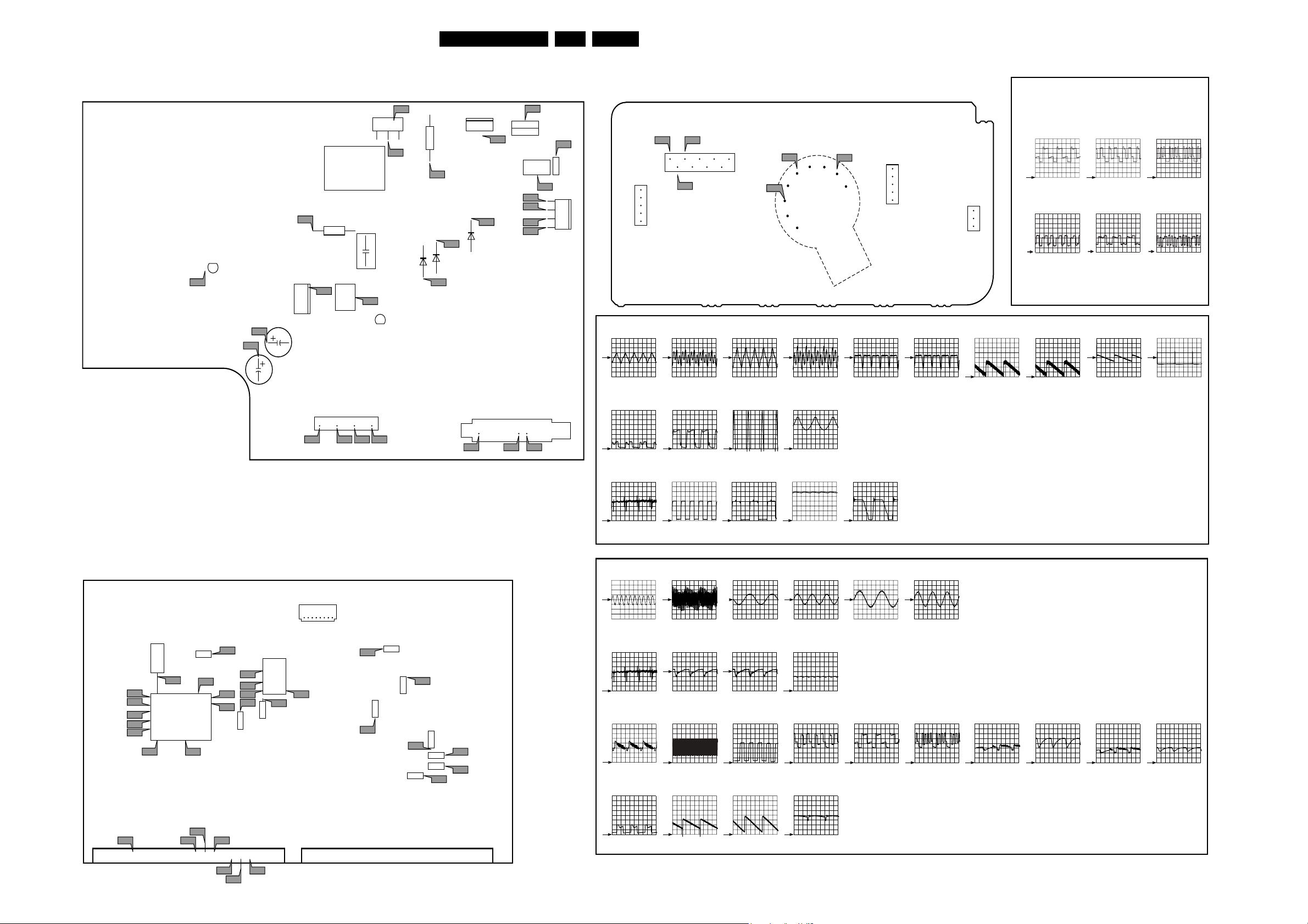
Block Diagrams, Testpoint Overview, and Waveforms
27A10E BB 6.
Testpoint Overview LSP, SSB, and CRT Panel
TESTPOINT OVERVIEW LSP (Component Side) TESTPOINT OVERVIEW CRT (Track Side)
L3
7410
C
BE
7481
EB
C
L2
F2
F4
F3
F1
1357
L1
3401
7501
LSP
V11
V13
13579
2468
0245
5
4
3
2
1
A1
V12
A2
7330
V14
8
7
V15
6
5
4
A3
A4
P6
7965
EB
P3
7921
4
153
P2
5912
P4
3971
SW RS
7967
3
OUT
2489
P7
6485
GKA
C
2
P5
7942
2715
A5
A6
3916
P1
6448
6447
L9
L10
7470
GS
D
L7
L8
6445
9
10
CRT Socket
V16
11
CRT
V11
0244
5
4
12
A5
3
2
1
A6
0278
1
2
3
F1
0,5V / div DC
20µs / div
V14
50V / div DC
20µs / div
F2
V12
0,5V / div DC
20µs / div
V15
50V / div DC
20µs / div
F3
V13
0,5V / div DC
20µs / div
V16
50V / div DC
20µs / div
F4
2718
TESTPOINT OVERVIEW SSB (Component Side)
0205
18
V6
1327
V2
54
S1
56
62
S4
63
S2
64
S3
1
I4
3348
V3
V6
V7
3233
31
7301
16
V8
I5
V9
V11
V12
I6
3301
9
10
14
16
3340
7405
1
V10
V4
7702
14712
A1
A2 A4 A3
TUNER
11 5 4
I1 I3
50mV / div AC
0.5ms / div
L1
50mV / div AC
0.5ms / div
L2
0.5V / div AC
0.5ms / div
L3
0.5V / div AC
0.5ms / div
L7
0.1V / div AC
0.5ms / div
L8 + 200V DC
0.1V / div AC
0.2ms / div
0.5V / div DC
5ms / div
0.5V / div DC
5ms / div
L9 - 12V DC
I2
0.5V / div DC
20µs / div
I1
20V / div DC
20µs / div
I2
100V / div DC
20µs / div
I3
5V / div DC
5ms / div
P1
L10 + 13V DC
P2
P3 17V DC
10V / div DC
5ms / div
10V / div DC
5ms / div
P4 140V DC
P5 8V
P6 3V3 DC
0.2V / div DC
5µs / div
SSB
A7
0.5V / div AC
1ms / div
2696
A7
A7
2678
2665
A8
2613
A12
2610
2612
2611
A11
A10
A9
I1
0.2V / div DC
5µs / div
V2
0.5V / div DC
20µs / div
S1
1V / div DC
5µs / div
A8
0.1V / div AC
20µs / div
I4
100mV / div AC
20µs / div
V3
0.5V / div DC
0.5µs / div
S2
1V / div DC
5µs / div
A9
headphone
volume max.
1V / div AC
0.2ms / div
I5
0.5V / div DC
20µs / div
V4
1.0V / div DC
5µs / div
S3
50V / div DC
5ms / div
A10
headphone
volume max.
1V / div AC
0.1ms / div
I6
1.0V / div DC
5.0µs / div
V6
1.0V / div DC
0.5µs / div
S4
0.1kV / div DC
2µs / div
A11
audio
volume max.
0.5V / div AC
0.2ms / div
V7
0.5V / div DC
20µs / div
P7 5V DC
A12
audio
volume max.
0.5V / div AC
0.1ms / div
V8
0.5V / div DC
20µs / div
V9
0.5V / div DC
5µs / div
V10
0.2V / div DC
20µs / div
V11
0.5V / div DC
20µs / div
V12
0.5V / div DC
20µs / div
I1 V8
80 68
V7
V6
58 57 56 53 52 51
S3
S2
SSB CONNECTOR
41 40 1
S4
0.5V / div DC
20µs / div
0.5V / div DC
5ms / div
0.5V / div DC
5ms / div
1.0V / div DC
5ms / div
CL 36532080_007.eps
081203
Page 28
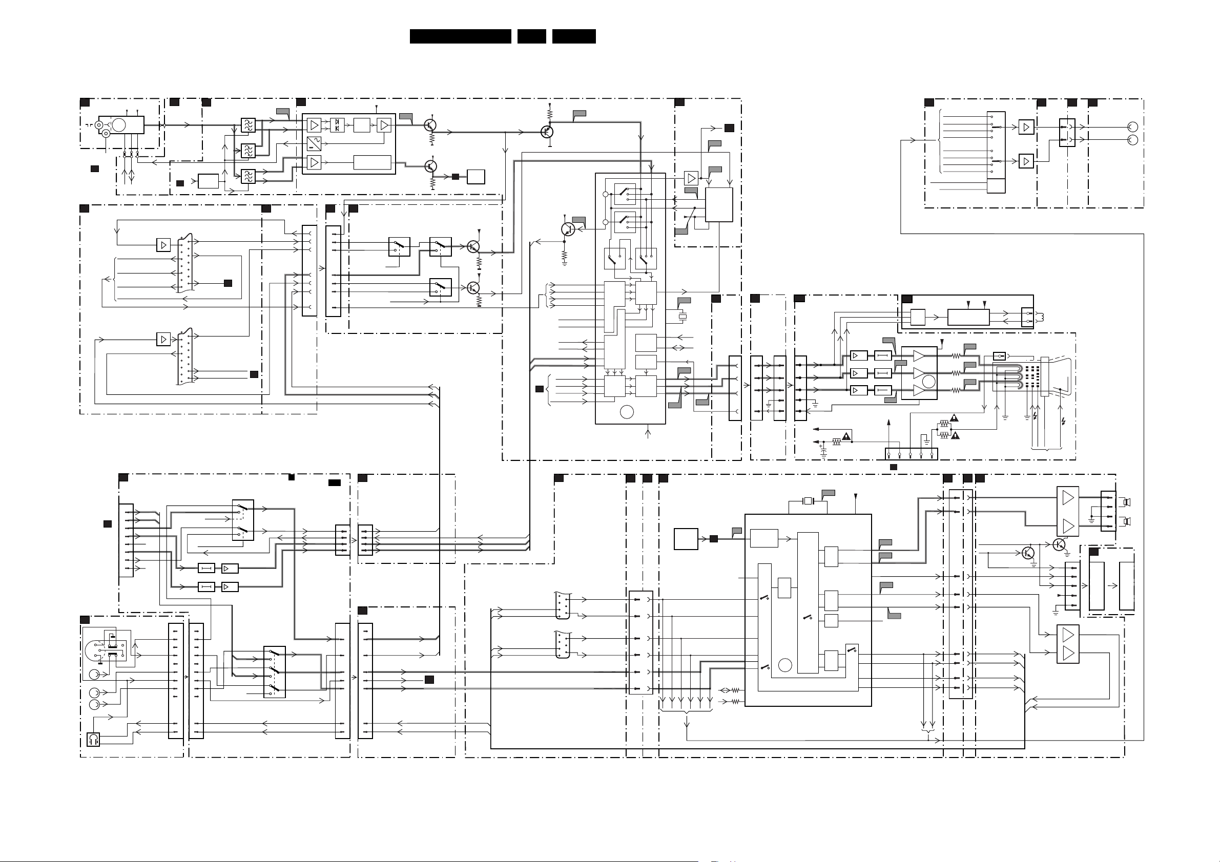
Block Diagrams, Testpoint Overview, and Waveforms
Block Diagram Video
28A10E BB 6.
VIDEO
A4
SSP TUNER
1225
TO RF INPUT
DIGITAL TUNER
K8
A5
SCART VIDEO
BLOCK-
DIAGRAM
SIDE I/O
D
SVHS
8
3
2
VIDEO
IN
L
R
+33v
+5V
69
ERR
TUNER
13
51
4
3534
SCL
SDA
CVBS_TER_OUT
R_SC1_V_IN
G_SC1_IN_Y_IN
B_SC1_IN_IJ_IN
FBL_SC1_AV_IN
CVBS_SC2_MON_OUT
C_SC2_MON_SVHS_IN
IBO+ INTERFACE
DIGITAL INTERFACE
S2
1600
5
FROM
7
1600
K6
9
SEE
15
17
IBO+
18
20
22
Y_CVBS_FRONT_IN
11
10
9
6
5
4
FRONT_DETECT
11
0226
66
AGC
R1_OUT
L1_OUT
CVBS1
Pr
NC
Pb
CVBS2
NC
C_FRONT_IN
L_FRONT_IN
R_FRONT_IN
HP_OUT_L
HP_OUT_R
C7
68
SEL-IF-LL
IF-TER
C3
SBB
CONN
C2
7413
7414
FILTER
SELECTION
VIDEO FEATURES
1451
1454
1455
7
8
7
8
7
8
A4 C7
SCART1
21
7224
20
CVBS_SC1_AV_IN
19
16
FBL_SC1_AV_IN
15
11
8
STATUS 1
7
SCART2
21
7226
20
19
16
15
11
8
7
Y_CVBS_FRONT_IN
CVBS_SC2_ANA_IN
0240
0240 0240
1
2
3
4
5
6
7
8
9
10
11
C3
Y_CVBS_SC2_AV2_IN
COMM_LINE
SEL_SVHS_RR_STATUS2
FOR THE COMPLETE BLOCK DIAGRAM OF S DIGITAL INTERFACE,
CVBS1
SEL_DIC
CVBS2
SEL_DIC_CVBS
5030
5031 7046
1
2
3
4
5
6
7
8
9
10
11
12
13
7045
2
1
EF
EF
7041
HEF4053
R_FRONT_IN
R1_OUT
L_FRONT_IN
L1_OUT
C_FRONT_IN
N.C.
C3
14
15
7040
HEF4053
2
1
5
3
12
1
C1 C2
IF VIDEO
7301-A
I4
VIF1
1
VIF2
2
AGC
7
Pr_MPEG_IN
Pb_MPEG_IN
74
75
18
74
17
79
0226
BOCMA
8
9
VSIF1
VSIF2
SSB CON
SEE BLOCK DIAGRAM IBO
R_IN_MAIN
15
L_IN_MAIN
4
C_IN_MAIN
14
C2
SEL_MAIN_R1R2
SEL_MAIN_FRNT_RR
+
0205
1
3
5
7
0241
2
4
6
7
8
10
11
+8VA
Sound
Traps
QSS Demod. +
AM Detection
C2
0205
1
3
5
7
A5
1
2
4
6
7
8
10
11
23
I5
16
11
7401-C
5
2
9
Y_CVBS_FRONT_IN
C_SC2_SVHS_IN
C_FRONT_IN
R/G/B/FBL_SC1
C_FRONT_IN
Y_CVBS_FRONT_IN
CVBS_SC2_MON_OUT
CVBS_SC2_MON_OUT
Pr_MPEG_IN
Pb_MPEG_IN
Y_CVBS_FRONT_IN
C_CVBS_FRONT_IN
L_FRONT_IN
FRONT_DTECT
R_FRONT_IN
HP_OUT_R
HP_OUT_L
7645-B
7645-A
0278
1
2
AQUADAG
R
G
B
FROM DEFLECTION
7711
VG2
C7
FOCUS
0226
SCAVEM
COIL
CRT
DEFLECTION
5
2
7701
+27V
6
2
HP_OUT_L
HP_OUT_R
A4 A5
11
12
25kV
EHT
7702
AN5277
0247
5
4
3
2
1
7703
TDA1308T
R_CL_VL_OUT
L_CL_VL_OUT
0246
74
3
2
112
D
SIDE I/O
0241 0242
HP_OUT_R
7
HP_OUT_L
1
R
L
R
L
ACTIVE SUBWOOFER CONNECTION
B2
SCAVEM
+
7330
TDA6107Q
2
V11
1
3
EHT-INFO
to 0241
DEFLECTION
C6
R_SC1_AV1_IN
R_SC2_AV2_IN
R_FRONT_IN
SC1_OUT_R
L_SC1_AV1_IN
L_SC2_AV2_IN
L_FRONT_IN
SEL_MAIN_FRNT_RR
SEL_MAIN_R1R2
+200VA
8
R
9
G
ERR
7
7
B
5
3341
3342
Filament
C7 A4 A6
SC1_OUT_L
SC1_OUT_R
SC1_OUT_L
+13V
SCAVEM
PROCESSING
V14
3336
V15
3334
V16
3332
0226
5
6
7
13
14
20
25
22
26
7630
12
14
13
15
11
1
5
2
4
9
SELECT
10
+200V
0165
8
6
11
10 9 5 7 1
AUDIO OUTPUT
AUDIO_R
AUDIO_L
SOUND_ENABLE
POWER_DOWN
R_SC1_AV_OUT
L_SC1_AV_OUT
R_SC2_OUT
L_SC2_OUT
3
+8VA
7305
CVBS_TER_OUT
3327
+8VA
7307
SIF
3302
7401-B
2
4
1
7401-A
12
13
AUDIO
C5
PAR T
+8V
15
7412-A
10
14
11
3413
+8V
7412-B
3416
CVBS_SC2_ANA_IN
V_PIP_MAIN_IN
U_PIP_MAIN_IN
C3
+8VA
CVBS_SC2_ANA_IN
C3
L_SC1_AV_OUT
L_SC1_AV_OUT
L_SC2_OUT
R_SC2_OUT
3340
7331
+8VA
7368
3365
R_SC1_IN
G_SC1_IN
B_SC1_IN
FBL_SC1_IN
N.C.
N.C.
N.C.
N.C.
U_PIP+MAIN-IN
V-PIP+MAIN-IN
R-TXT-OSD
G-TXT-OSD
B-TXT-OSD
FBL-TXT-OSD
AUDIO
A5
SCART AUDIO
SCART 1
6
5
4
3
2
1
SCART 2
6
5
4
3
2
1
VIDEO PROCESSING
V1
CVBS_INT
CVBS/Y2
7301-B
+
V2
+
54
41
RGB/
42
YUV
43
INT
44
40
39
45
YUV
46
INTER-
FACE
47
SAT.
48
CTRL
35
RGB
36
INPUT
37
38
L_SC1_AV1_IN
R_SC1_AV1_IN
L_SC2_AV2_IN
R_SC2_AV2_IN
L_FRONT_IN
R_FRONT_IN
COLOUR
DECOD-
ING
Y
U
V
I2C
BUS
CTRL
CAT.
CALIB.
RGB
OUTPUT
ERR
BOCMA
7,8,9
34
EHT-INFO
A4 C7 C5
0226
29
27
28
23
16
15
2924
26
21
20
49
51
52
17
18
30
33
32
31
AUDIO PROCESSING
Y-IN
+5V
V12
COMB-ON
V7
FROM
IF VIDEO
V3
V6
PAR T
7401
SCL
SDA
V11
1732
CVBS_2_OUT
V10
V9
12
14
7405
COMB
16
FILTER
5
C7
R
G
B
V8
C1
SC1_IN_L
SC1_IN_R
SC2_IN_L
SC2_IN_R
SC3_IN_L
SC3_IN_R
SDA
SCL
96
S1F1
C3
N.C.
C-IN
3602
3601
1
A4
SSB CONN
56
57
58
60
CRT
B1
R
G
B
EF
EF
EF
0244
V12
5344
FF
5343
5345
V13
+13V
123 4 5
02420226 0205
0245
R
1
1
G
2
2
B
3
3
4
4
5
5
BKL
+200V
+200VA
7732
7731
7733
3340
2340
A2
+8VC
B76
18.432MHz
7651
A8
50
47
44
45
41
42
38
39
2
1
MSP34XX
DEMO-
DULATOR
ADC
ERR
54
14
DSP
DIGITAL
SOUND
PROC.
55 31
DAC
DACM-SUB
DAC
DACM-S
DAC
DAC
A11
AUDIO_R
20
R
A12
AUDIO_L
21
L
AUDIO_SW AUDIO_SW
23
A9
17
HEADPHONE-R
R
L
18
HEADPHONE-L
A10
N.C.
24
R_SC1_AV_OUT
28
R
L_SC1_AV_OUT
29
L
R
R_SC2_AV_OUT
25
L
26
L_SC2_AV_OUT
CL 36532080_002.eps
031203
Page 29
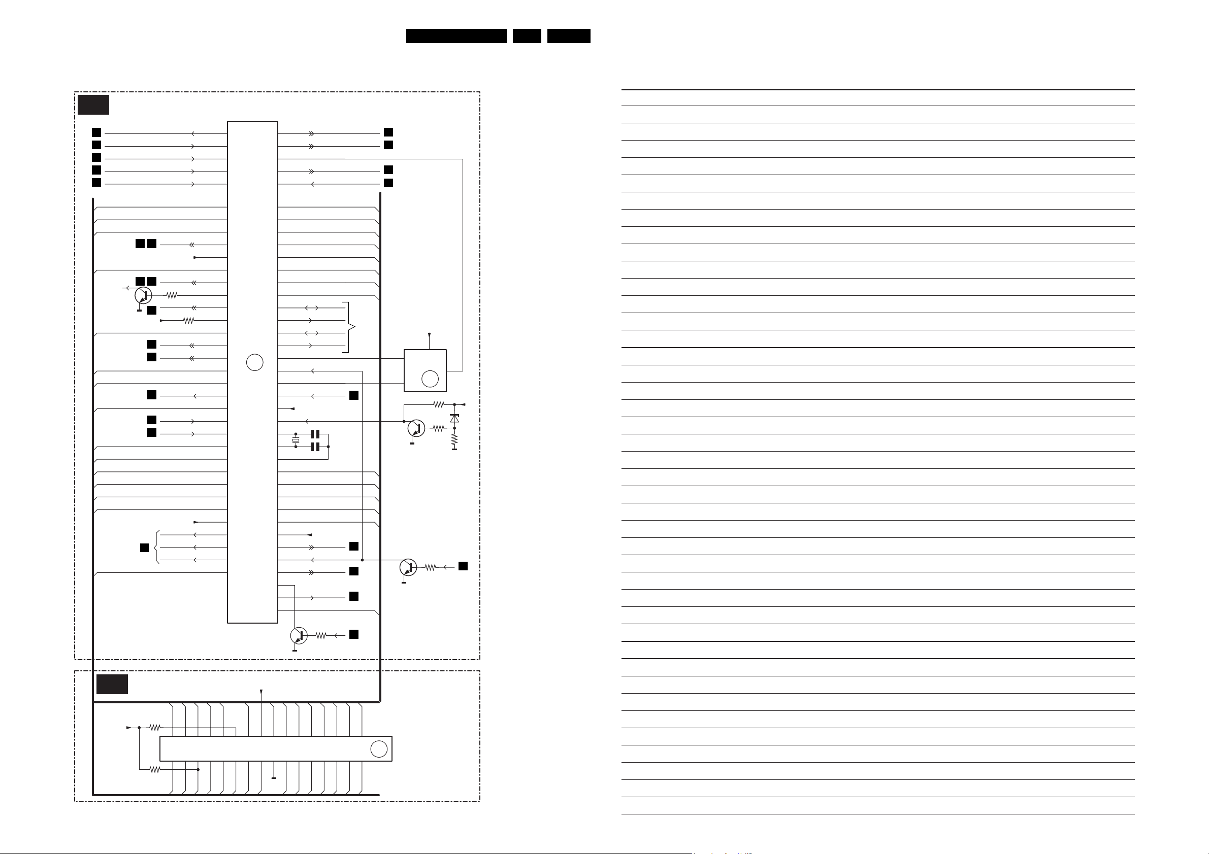
Block Diagrams, Testpoint Overview, and Waveforms
Block Diagram Micro Processor
29A10E BB 6.
Personal Notes:
C3
A7
A5
A5
A7
A7
A14
OENOT
WENOT
A7
COMM-LINE
A6
A5
A4
CENOT
A15
A3
A2
A1
A0
U_CONT
7022
A13
A12
TILT
SEL-SVHS-RR_STATUS2
STATUS_PIP-AFT_PIP-50-60HZ
KEYBOARD
FRONT-DETECT
STAND-BY
A6A1
+3.3V-STBY
SEL-MAIN-FRNT-RR
C6C2
3029
LIGHT-SENSOR-VDEGAUSS
C7
+3.3V-STBY
ON-OFF-LED
CVBS2OUT
G-SC1-IN-Y-IN
+3.3V-STBY
B-TXT-OSD
G-TXT-OSD
R-TXT-OSD
SYS1
SYS2
C2
C2
C7
C2
C1
C1
7064
1
2
4
5
6
8
9
10
13
14
15
16
17
18
22
23
24
25
26
27
28
29
31
32
33
36
37
38
39
40
45
46
47
48
49
U_CONT
ERR
12
100
98
97
96
93
92
91
90
89
88
87
86
85
84
83
82
81
80
79
78
76
75
73
71
70
69
68
67
66
65
64
63
59
55
54
53
52
51
PANORAMA
SOUND-ENABLE
HIS-OFF
AGCuP
SDA-2
SCL-2
SDA
SCL
RC5
+3.3V-STBY
RESET
2041
1057
2042
+3.3V-STBY
SEL-IF-LL
SEL-MAIN-R1R2
FBL-TXT-OSD
7053-A
3025
HFB
IO8
IO7
IO6
IO5
IO4
IO3
IO1
SEE
I2C
DIAGRAM
I
A12
A10
A11
C2
C2
C1
A16
A2
IO2
A8
A9
A2
A6
C2
C1
+3.3V-STBY
7066
5
6
SDA
NVM
SCL
7063
7053-B
ERR
10,11
3055
WC
3081
3055
7
+3.3VSTBY
3083
VFB
6031
A3
C4
FOR 100 PAGES
TELETEXT
+3.3V-STBY
MEMORY
A11
3090
1
3091
OENOT
+3.3V-STBY
A9
A8
A13
WENOT
2 3 4 5 6 7 8 9 10 11 12 13 14 16 16
90
A10
CENOT
IO8
IO7
IO6
A15
7070 SRAM
IO5
IO4
N.C.
A14
A16
A12
IO2
IO1
IO3
A5
A6
A7
A1
A0
A2
A4
ERR
15
171819202122232425262728303132
A3
CL 36533080_006.eps
021203
Page 30
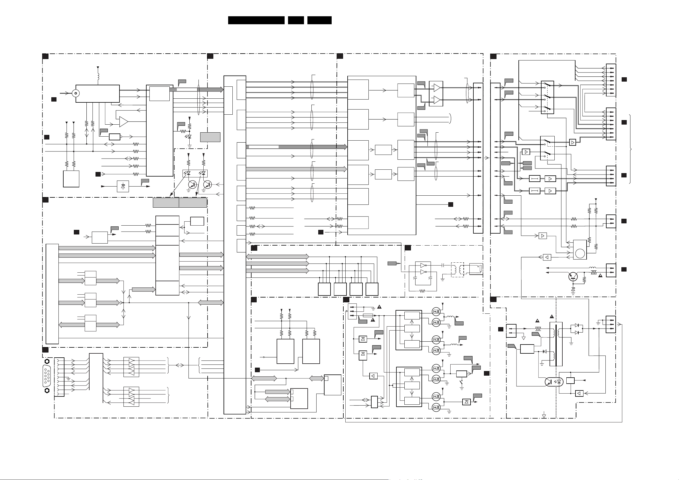
Block Diagrams, Testpoint Overview, and Waveforms
Block Diagram IBO+ Panel
30A10E BB 6.
IBO+ PANEL
FRONT END
K8
1800
RF-IN
+5V +5V
EEPROM
TD1316L
3812
38203821
6
5
FROM
MAIN
TUNER
A4
3811
K6
I2C_IBO_SDA2
I2C_IBO_SCL2
PCMCIA INTERFACE
K9
K9
68P PCMCIA
CONNECTOR
135
34 68
RS232 INTERFACE
K5
9
5
1
6
VCCEN
A_MD (0-7)
A_MDO (0-7)
CONTROL LINES (6X)
PCMCIA-A (0-7)
PCMCIA-A (8-14) PCI-AD (8-14)
PCMCIA-D (0-7)
CONTROL_LINES
1500
1
2
3
4
5
6
7
8
9
N.C.
9
3817
7801
M24C256
7900
74LVC573ADB
CONTROL
LATCH
7901
74LVC573ADB
CONTROL
LATCH
7903
74LVC245APW
CONTROL
TRANS
CEIVER
DCD
RXD
TXD
DTR
DSR
RTS
CTS
+5VClean
TUNER
8 10 5
7904
ST8900
CURRENT
SWITCH
BUS
5800
11
13
AGC
XTAL
3816
7804
I810
74HC1GU04
2
INVER
I2C_LOCAL_SDA
I2C_LOCAL_SCL
RESET_FE-n
K1
6
8
PCI-AD (0-7)
PCI-AD (24-31)
TER
I970
CTS
RXD
RTS
TXD
DCD
DSR
DTR
14
15
2
+
3
-
3
13
14
13
14
IF1
IF2
IF-AGC
AGC-TUN
7803-A
LM393D
COMP-OUT
1
X-IN
4
3818
3819
3810
3813
2
I2C_LOCAL_SCL
I2C_LOCAL_SDA
PCMCIA_5V
FAULT_SEG
PCI-AD (15-25)
7503
ST202ECD
7506
ST202ECD
9
12
10
11
9
12
10
11
8
7
8
7
7800
TDA10046HT
62
COFDM
CHANNEL
61
DECODER
21
54
4
3
COFDM
8
6
9
I833
+1V8FE+3V3
3900
3901
VPR_UA2_CTS
VPR_UA2_RXD
VPR_UA2_RTS
VPR_UA2_TXD
VPR_UA2_DCD
VPR_UA2_DSR
N.C.
VPR_UA2_DTR
38
25
*
GREEN ->
FLASK OK IN DSW
7902
STV0700
PCMCIA
CONTROLLER
IIC
INTERFACE
INTERRUPT
MANAGEMENT
TS
INTERFACE
UC SG
N.C.
MPEG
I821
TDA DAT (0-7)
TDA_CLK
TDA_VALID
TDA_SYNC
TDA_ERR
+3V3
I807
3831
3832
6800
RED
*
LOCK
+3V3-VPR
+3V3-VPR
3098 3099
GREEN
21
*
6101
43
7105
*
RED/ORANGE ->
BOARD IS FLASHING
7905
FXO-31FT
OSC
27MHz
STV_CLK
RESET_STV
TS_DATA (0-7)
CONTROL
DV3_DAT (0-7)
CONTROL
STV_CS
CONTROL
VIPER
K1
*
RED ->
FLASH ERROR
*
RED/
ORANGE
7106
PCI_AD (0-31)
VPR_UA2_CTS
VPR_UA2_RXD
VPR_UA2_RTS
VPR_UA2_TXD
7100
PNX8525 (VIPER 1.0)
PNX8526 (VIPER 1.1)
I2S
OUT1
DV3
I2S
OUT2
DV
OUT1
DV
OUT2
SYNC
I2C2
I2C1
SPDIF
OUT
VIPER
VPR_I2S_OUT1_OSCLK
VPR_I2S_OUT1_SCK
VPR_I2S_OUT1_WS
VPR_I2S_OUT1_SD
VPR_I2S_OUT2_OSCLK
VPR_I2S_OUT2_SCK
VPR_I2S_OUT2_WS
VPR_I2S_OUT2_SD
VPR_DV1_OUT (0-9)
VPR_DV1_CLK
VPR_DV2_OUT (0-9)
VPR_DV2_CLK
VPR_HSYNC
VPR_VSYNC
VPR_BLANK
3159
I2C_IBO_SDA1
3157
I2C_IBO_SDA1
3155
I2C_LOCAL_SDA
3154
I2C_LOCAL_SCL
VPR_SPD1F_OUT
SDRAM VIPER
K2
VPR_SDRAM_D (0-63)
VPR_SDRAM_A (0-13)
VPR_SDRAM_DQM (0-7)
VPR_SDRAM_CONTROL_LINES (7x)
K3
FLASH MEMORY
+5V +5V
1301-1 7
PCI_AD (1-19)
PCI_AD (24-31)
3313
3317
57656
7305
M24C64
BOOT
EEPROM
I2C_LOCAL_SDA
I2C_LOCAL_SCL
VPR_SYS_EEPROM_WC_n
K1
PCI_AD (0-31)
VPR_NOR CONTROL LINES
VPR_NAND_CONTROL LINES
3314
3320
7303
AM29LV160D
A
NOR FLASH
D
I2C_LOCAL_SDA
I2C_LOCAL_SDL
3322
7306
M24C64
SYSTEM
EEPROM
2MB
I2S
PRIMARY
I2S
SEDUNDARY
VIDEO
PRIMARY
VIDEO
SECUNDARY
SYNC
K7
(0-1)
7200
SDRAM
128MBIT
3323
PCI_AD
(24-31)
ANALOG BACK END
K6
7602
PNX8510
SECUNDARY
SECUNDARY
3617
26
3618
27
RESET
4
4x SDRAM K4S281632E
(6-7) (2-3) (4-5)
7203
SDRAM
128MBIT
K7
1700
7304
K9GF2808UOC
IO
NAND FLASH
16MB
I2C_
IBO_SCL1
I2C_IBO_SDA1
PRIMARY
I2S
INPUT
I2S
INPUT
PRIMARY
DIGITAL
VIDEO
INPUT
DIGITAL
VIDEO
OUTPUT
SYNC
INPUT
I2C
7201
SDRAM
SDRAM
128MBIT
128MBIT
POWER SUPPLY
1
2
1702
3
i719
6702
L78L05ACD
18
7700
LF90C
15
INH
2
PCF8574T
15
14
7202
+12V
i770
+5VSTDBY
i717
7702
7707
I/O
EXP
DIGITAL
ENCODER
DIGITAL
ENCODER
ANABEL
+9V
6
4
5
I547
14
21
14
21
7705
ISL6444
8
8
7600
LM833D
I643
96
6
2
I641
91
ANABEL_R2_OUT
95
ANABEL_L2_OUT
I614
I613
44
49
47
46
I616
I617
38
40
84
ANABEL_P10a
85
ANABEL_P10b
2x
3505
7701_A
5
2
7701_B
7703_B
24
27
7703_A
7704_A
5
2
7704_B
7706_B
24
27
+
-
+
-
VIDEO
DISPLAY CHANNEL
ANABEL_CVBS_1
ANABEL_R_C_1
ANABEL_G_Y_1
ANABEL_B
VIDEO RECORD
CHANNEL
ANABEL_CVBS_2
ANABEL_C_2
I2S_IBO_SDA1
I2S_IBO_SCL1
2516
2
4
+12V
7706_A
2x
AUDIO
100
DAC
2x
AUDIO
DAC
4x
VIDEO
DAC
2x
VIDEO
DAC
K5
SPDIF INTERFACE (ONLY VALID FOR VIPER 1.1)
7505
74NCU04D
1
3
INVERTER
PWM
CONTROL
SOFT
START
PWM
CONTROL
7712
ISL6444
PWM
CONTROL
SOFT
START
PWM
CONTROL
AUDIO
ANABEL_R1_OUT
1
ANABEL_L1_OUT
7
N.C.
K?
3654
3655
5510
1
3
(DIGITAL AUDIO
5702
VPR_CORE_VCC
i725
+12V
I716
5701
+12V
7710
NCP303
RESET
1703
+12V
7708
LD1117
5701
1600
5
7
9
15
17
18
20
22
14
11
12
1503
SPDIF
OUT
OUTPUT)
+5V
I765
I727
RESET_n
Manual Reset
Switch
I753
+3V3
K2
+5V Clean
DIGITAL INTERFACE
S2
I648
1600
5
R1_OUT
I649
7
L1_OUT
I650
9
CVBS1
15
Pr
17
NC
18
Pb
I656
20
CVBS2
22
C2_OUT
I658
14
IRQ
I653
I651
11
12
I652
IBO + POWER
S1
SUPPLY
0203
TO 0231
A1
POWER
SUPPLY
H2
SDA
SCL
2
1
R_FRONT_IN
L_FRONT_IN
C_FRONT_IN
Y_CVBS_
FRONT_IN
7050
I654
I657
Pr
Pb
ON-OFF_12V
5
CONTROL
7902
STR_G6551
7040
HEF4053
2
1
5
3
12
N.C.
13
7041
HEF4053
12
13
2
1
5030 7045
5031
7052
7053
IRQ
+5V_STANDBY
+8V
3901
H1
1
4
EF
7046
EF
7051
5904
1 7-8
3
6
5
7903
5
4
HOT COLD
R_IN_MAIN
15
L_IN_MAIN
4
14
C_IN_MAIN
14
15
SEL_DIG_CVBS
9-10
1
2
Y_CVBS_FR_IN
FRONT_DETECT
R_IN_MAIN
L_IN_MAIN
C_IN_MAIN
Y_CVBS_IN_MAIN
7048
CVBS_SC2_MON_OUT
CVBS_SC2_ANA_IN
3013
3014
7008
PCF8574a
SEL_DIGITAL
11
I/O
9
EXPANDER
10
ERR
12
24
7024
6024
6904
6903
7901
6906
STAB
7905
R_FRONT_IN
L_FRONT_IN
R_FRONT_IN
HP_OUT_L
HP_OUT_R
Pr_MPEG_IN
Pb_MPEG_IN
+5V_STANDBY
3012
3043
SDA_2
SCL_2
3011
3010
15
14
5029
3025
3022
+12V
+8V_UNREG
ON_OFF_12V
CL 36532080_001.eps
121203
0240
2
4
6
8
7
10
11
0241
11
10
7
8
6
4
2
0205
1
3
5
7
0239
3
2
0206
2
4
1700
1
2
3
TO 0240
D
SIDE I/O
TO 0240
A5
LSP
TO 0205
C2
SSB
TO 0239
A4
LSP
TO 0206
A1
LSP
TO BLOCK DIAGRAM VIDEO/AUDIO
Page 31

Block Diagrams, Testpoint Overview, and Waveforms
31A10E BB 6.
Testpoint Overview IBO
I100 C2
I101 D5
I102 C2
I103 C1
I104 E5
I105 E5
I106 C4
I107 B4
I108 D5
I109 C6
I110 C6
I112 C7
I113 C7
I115 C7
I116 C6
I117 C6
I118 C5
I119 C6
I120 D4
I121 D4
I122 E4
I123 D4
I124 B5
I125 B5
I126 C5
I127 E5
I128 E5
I129 D5
I140 B6
I141 D5
I142 C3
I143 D5
I145 D5
I146 C5
I147 C5
I148 C5
I149 C6
I150 D5
I151 D6
I157 D4
I158 D7
I160 E6
I161 E6
I162 E6
I163 E6
+
I165 D4
I166 C3
I167 D3
I168 B1
I169 D4
I170 E5
I171 E5
I172 D6
I173 E6
I174 D6
I175 D6
I176 C6
I177 C6
I178 D5
I179 D6
I180 E5
I181 D5
I183 E5
I184 D4
I185 D5
I186 C6
I187 C7
I188 C7
I189 C6
I198 D5
I199 D6
I200 B5
I201 B4
I202 C3
I203 D3
I308 E5
I310 D5
I311 E5
I313 E5
I314 B4
I315 D5
I316 E4
I317 B2
I318 E5
I319 B4
I320 A6
I322 E3
I323 E5
I324 E3
I325 E3
I326 E3
I327 E6
I330 A3
I331 A2
I332 A3
I333 A2
I400 B5
I401 B5
I402 B4
I403 B5
I404 B5
I406 B5
I407 B5
I408 B5
I410 A5
I411 A5
I412 A5
I414 A5
I415 B5
I416 B5
I417 A5
I420 A5
I421 B5
I422 B5
I423 A5
I424 B5
I425 A5
I426 A6
I427 A6
I428 A6
I429 A6
I430 A5
I431 A5
I432 A5
I433 B5
I434 A5
I435 B5
I436 A5
I437 A4
I438 A5
I439 A5
I440 A5
I441 B5
I442 A5
I500 A4
I501 A4
I502 A5
I503 A5
I504 A4
I505 A4
I506 A4
I507 B4
I509 B4
I511 B4
I513 B4
I515 A7
I516 A6
I517 A6
I518 B7
I519 A7
I520 A7
I521 A4
I522 A4
I544 A7
I545 A7
I546 A7
I547 B6
I548 A7
I549 C1
I550 B1
I551 B1
I552 B1
I553 B1
I554 B1
I555 B1
I556 B1
I560 B3
I561 B3
I562 B3
I563 B3
I564 B3
I566 A4
I567 A4
I568 A4
I569 A4
I570 A4
I571 A4
I600 E7
I601 E6
I602 D7
I603 D6
I604 D7
I605 D6
I606 D7
I607 D6
I608 E7
I609 E6
I610 D6
I611 E6
I612 E6
I613 E6
I614 E6
I615 E7
I616 E6
I617 E7
I618 E6
I619 B2
I620 D7
I622 D6
I623 D6
I624 D6
I625 D6
I626 D6
I627 E7
I628 D7
I629 D6
I631 E6
I632 D6
I633 E6
I634 E7
I635 D7
I636 D7
I637 D7
I638 D7
I639 D7
I640 D7
I641 D7
I642 D7
I643 D7
I644 D7
I645 D7
I646 E6
I647 E6
I648 D8
I649 D8
I650 E8
I651 D8
I652 D8
I653 E8
I654 E8
I655 E8
I656 E8
I657 E8
I658 E8
I662 C7
I663 D7
I700 D2
I701 C7
I704 D2
I705 D8
I706 C7
I707 D2
I709 E2
I712 E8
I713 E8
I715 D2
I716 B3
I717 C7
I718 E1
I719 E8
I720 E8
I721 E8
I722 D2
I723 C7
I724 C7
I725 E3
I727 A4
I728 A4
I729 E2
I730 E2
I737 D1
CL 36532080_009.eps
081203
I744 D1
I747 E1
I751 E1
I752 E1
I753 C7
I755 D1
I756 E1
I765 A6
I766 E1
I767 E1
I770 D1
I773 A7
I774 B3
I775 B1
I776 A4
I777 E1
I784 A3
I785 A4
I786 A2
I787 D2
I788 A3
I800 B6
I801 B6
I802 B6
I803 C7
I804 C6
I805 B6
I806 B6
I807 B6
I808 C6
I809 B8
I810 B8
I811 A8
I812 B6
I813 C7
I814 C7
I815 B7
I816 B8
I817 B6
I818 B7
I819 B7
I820 B7
I821 B6
I822 B6
I823 B6
I824 B6
I825 B6
I826 B6
I827 B7
I828 B6
I829 B6
I830 B6
I831 B6
I832 B6
I833 B6
I834 B6
I835 B6
I900 D1
I901 D1
I902 D1
I903 C1
I904 D1
I905 D1
I906 D1
I907 C1
I908 D1
I909 D1
I910 D1
I911 C1
I912 D1
I913 D1
I914 D2
I915 C1
I916 D2
I917 D2
I918 D1
I919 C2
I920 D2
I921 D2
I922 D2
I923 C2
I924 D2
I925 D2
I926 D2
I927 C2
I928 D2
I929 D2
I930 D2
I932 D2
I934 D2
I935 D2
I936 D2
I937 C2
I938 D2
I939 D2
I940 D2
I941 C2
I942 D2
I943 D2
I944 D2
I945 C2
I946 D2
I947 D2
I948 D2
I949 C2
I950 D2
I951 D2
I952 D2
I953 C2
I954 D2
I955 D2
I956 D3
I957 C3
I958 D3
I959 D3
I960 D3
I961 C3
I962 D3
I963 D3
I964 D1
I965 D1
I966 B2
I967 B1
I969 B3
I970 A2
I971 B1
I972 B2
I973 B3
I974 B2
I975 B1
I976 B2
I977 A2
I978 B2
I979 A2
I980 A2
I981 B1
I109
1V / div DC
20ns / div
I330
1V / div DC
10µs / div
I331
1V / div DC
10µs / div
I613
200mV / div DC
20µs / div
I614
200mV / div DC
20µs / div
I616
200mV / div DC
20µs / div
I617
500mV / div DC
20µs / div
I650
200mV / div DC
20µs / divv
I651
1V / div DC
20µs / div
I652
1V / div DC
20µs / div
I654
200mV / div DC
20µs / div
I655
500mV / div DC
20µs / div
I656
200mV / div DC
20µs / div
I657
500mV / div DC
20µs / div
I658
500mV / div DC
20µs / div
I716 = 5V I807 = 0V
I717 = 9V
I719 = 11V8
I725 = 1V8
I727 = 3V3
I753 = 5V
I765 = 3V3
I770 = 5V
I833 = 1V8
I870 = 4V7
I810
100mV / DIV ac
250ns / div
Page 32

I2C IC’s Overview
U_CONT
C3
81
82
C4
7064
SAA5667
U_CONT
83
84
Block Diagrams, Testpoint Overview, and Waveforms
3017
SCL
3085
SDA
AUDIO
DEMODULATOR
UPD431000A
3019
SCL-2
3018
SDA-2
7070
SRAM
ERR
15
ERR
IF-VIDEO
C1
6
3330
3329
17 18
7301
TDA8845
VIDEO PROC.
BOCMA
ERR
7,8,9
C5
MSP3451G
AUDIO
DEMODULATOR
3602
3601
12
7651
ERR
14
C7
SSBCONNECTOR
0226 0226
A4
SSP-TUN
34
35
32
33
3267
3268
45
1225
UV1300
(TUNER)
ERR
13
A7
3038
32A10E BB 6.
+5V_RC_STB
3037
COMPAIR
SERVICE
CONN.
FOR
0229
1
2
3
0239
SCL-2
SDA-2
DIGITAL INTERFACE
S2
0239
3043
3010
14 15
PCF8574AT
+5V_STANDBY
3012
3011
7008
ERR
24
3014
3013
SCL
SDA
1800
12
11
ERROR CODE LIST
Error Error description Possible defective components
No error detected
1 X-ray protection/ EW and/or High beam
protection active
2 Vertical protection Vertical circuit is defective
3 Reserved
4 5V protection active +5V supply line is low or short circuit
5 Reserved
6 General I2C bus error I2C bus s/c or o/c on uP
7 BC-loop not stabilised RGB amplifiers, RGB guns or RGB driving
8 BOCMA I2C error IC7301 - TDA8885
9 BOCMA 8V supply failure IC7301 and R3331
10 NVM I2C error IC7066 - M24C32
11 NVM identification failure IC7066 - M24C32
12 Microprocessor internal RAM test failure IC7064 - SAA5667
13 Main Tuner I2C error IC122 5 - UV13xx / TEDE9
14 Sound processor I2C error IC7651 - MSP3415 / 3451
15 SRAM I2C error IC7070 - UPDxxxx
24 IO expander IC (on Dig. Interf. panel) IC7008 - PCF8574
25 IBO+ microprocessor IC7100 - PNX8525
LOT, Line deflection circuit, EW -circuit or CRT
amplifier circuit, picture tube or +200V missing
signals of BOCMA
K1
ERR
12
VIPER
7100
VIPER
PNX8525
+3V3-STB4
3065
78
SCL
80
SDA
D6
A4
3064
3084
3086
3154
I2C_LOCAL_SCL
3155
I2C_LOCAL_SDA
M24C32
6
5
7066
(NVM)
ERR
10,11
+3V3_VPR
FLASH MEMORY
K3
3309
65
PCF8563TS
OPTIONAL
7302
3310
3313
+5V
3314
3317
3320
65
7305
M24C64
BOOT
EEPROM
3322
3323
65
7306
M24C64
SYSTEM
EEPROM
K8
TDA10046HT
FRONT END
3810
3813
68
7800
COFDM
3818
3
3819
4
i2C_LOCAL_SCL2
i2C_LOCAL_SDA2
3821
3820
12
7801
M24C256
(NVM)
3812
+5V
3817
3816
89
1800
TD1316L
(TUNER)
3811
ANABEL
K6
ANALOG BACK END
3617
3618
27 26
7602
PNX8510
ERR
25
H1
K4
3157
3159
+3V3_VPR
3163
3162
G
S
D
SD
G
BSN20
7103
BSN20
7103
I2C_IBO_SCL1
I2C_IBO_SDA1
K7
POWER
SUPPLY
14 15
7707
PCF8574T
I/O EXP.
I2C_IBO_SCL1
I2C_IBO_SDA1
3655
3654
SCL
SDA
1600
12
1
CL 36533080_005.eps
081203
Page 33

Block Diagrams, Testpoint Overview, and Waveforms
Supply Voltage Diagram
33A10E BB 6.
POWER SUPPLY
A1
0212
2
4
AC MAINS
INPUT 220V
0231
2
4
1
3
HOT COLD
FRONT INTERFACE PANEL
J
0211
1
2
1002
MAINS HARMONIC
U
0001
13
4
18
10
3
STANDBY LED
MAINS
FILTER
6941
1941
6961
1961
6938
6972
MAINS SWITCH
0132
VS
GND
3004
0002
+8V Unreg.
7942
7942
3964
7967
5
2
3997
6977
+8V_UNREG
+5V_STBY
3
7978
+3.3V-STBY
3003
1008
7944
7966
6966
+13V_VERT
+5V_STBY
+5V_RC_STBY
VBAT (140V)
0212
1
2
0214
5
0206
2
4
STANDBY
+8V
6965
+5V
+27V
+3.3V-STBY
LINE DEFLECTION
A2
+8V
+3.3VSTBY
PANORAMA
5431
EW
+
LOT
LINE
LINE-
DRIVE
DRIVE 1
3
3414
7408
VBAT
+33V
6481
BZX79_F33
SSB TUNER SSB
A4
5261
+3.3V-STBY
+8V
+5V
7712
+27V
FOR ACTIVE
SUBWOOFER BOX
9
6
5262
1225
TUNER
UV1300
7280
7273
7702
AN5277
7226
7224
+33V
+5V
+8V
+8V
+27V
+5V
A5
A6
D
0241
2
SSB-SCART
3247
AUDIO
3736
3737
7703
TD1308T
SIDE I/O
0247
6
11
12
2
9
0242
2
3448
3449
3446
3447
+13V_SCAVEM
3445
3445
CONN
0226
40
38
36
41
6445
6448
3445
6447
+13V
VERT.
-13V
0241
1
+200V
2
FF
4
FIL2
5
SSB-CONNECTOR
C7
0226
40
38
36
41
C3
MEMORY
C4
AUDIO DEMODULATOR
C5
AUDIO CINCH OUT
C6
U-CONT.
7066
NVM
7064
uP
7070
UPD431000A
7651
+8V SOUND
FRAME DEFLECTION
A3
+8V
2531
+13V_VERT.
-13V -13V
CRT PANEL
B1
0244
+13V_
1
+200V
2
4
5
8
5042
75
5040
45
5050
8
101
31
FF
CRT
5601
5625
5602
2
7501
TDA8172
4
B2
3340
+3.3V-STBY
+3.3V-STBY
+3.3V-STBY
+8V SOUND
+8V SOUND
AUTO
SCAVEM
3362
+8V
+5V
+5V
+5V
+8V
7513
0252
+200V
SCAVEM
+13Va
7330
FRONT
A7
ROTATION
ROTATION
+8VA
+8V
+5V
3035
GND
VS
5322
5333
+8V
7017
7014
7012
7016
1009
POWER SUPPLY
K7
1
2
3
1700
7301
TDA8885
14
23
+8VA
53
0214
1702
5
5703
BOCMA
0235
-13V
1
1
+13V_VERT.
FRONT CONTROL (OPTION)
+5V_RC_STBY
IF & SYNC
C1
+3.3V-STBY
+8VA
3332
3331
+8V
VIDEO-FEATURES
C2
+8VA
+8V
+5V
+
IBO
S1
POWER SUPPLY
0231
2
1
4
CONTROL
7902
STR_G6551
DIGITAL INTERFACE
S2
0206
3025
4
2
5029
+12V
7705
ISL6444
14
CONTROL
8
21
CONTROL
7712
ISL6444
14
CONTROL
8
21
CONTROL
6702
L7805ACD
811
7700
LF90C
5
3022
PWM
SOFT
START
PWM
PWM
SOFT
START
PWM
3901
1
4
+5V STBY
5904
1 7-8
3
6
5
7903
5
4
HOT COLD
7701_A
5
2
7701_B
7703_B
24
27
7703_A
7704_A
5
2
7704_B
7706_B
24
27
7706_A
6024
7024
1700
6904
6903
7901
6906
+12V_UNREG
ON_OFF_12V
+8V
+5V_STANDBY
Manual Reset
Switch
7708
LD1117
5903
K2
RESET_n
5905
9-10
1
STAB
2
7905
+12V
5702
5710
+12V
5701
+12V
7710
NCP303
RESET
1703
+12V
5701
1
2
+12V
3
VPR_CORE_VCC
+5V
+3V3
+5V Clean
+9V+9V
1x
3x
8x
1x
1x
VIPER
K1
VPR_CORE_VCC
+3V3
SDRAM VIPER
K2
+3V3
FLASH MEMORY
K3
+3V3
+5V
IEEE 1394 (Option)
K4
+5V
INTERFACE
K5
+3V3
+5V
ANABEL
K6
+3V3
+9V
FRONT END
K8
+3V3
+5V
+5V Clean
PCMCIA
K9
+3V3
2
5802
7802
7904
CURRENT
SWITCH
5102
5101
5100
5200
5201
5202
5203
5300
5405
5404
5405
5500
5901
5905
5900
6
VIPER
SUPPLY
+3V3_VPR
TO VDD IC7200
TO VDD IC7201
TO VDD IC7202
TO VDD IC7203
+3V3_MEM
+3V3
+5V
+3V3_1394A
+3V3_1394D
+3V3
+5V_UART
+5V
+3V3
+9V
+3V3
+3V3FE
1V8FE
+5V
+5V Clean
+3V3
+3V3_STV
+3V3_CORE
+3V3_BUF
+5V
PCMCIA_5V
5902
PCMCIA_VPP
5901
PCMCIA_AVCC
CL 36532080_004.eps
101203
Page 34

Circuit Diagrams and PWB Layouts
7. Circuit Diagrams and PWB Layouts
Power supply
34A10E BB 7.
A
B
C
D
E
F
TO/FROM 0212 OF
FRONT INTERFACE PNL
G
H
3139 123 5577.3
12345678910 11
POWER SUPPLY
+t
3911
ZPB
0211
2
+t
1
0227
3912
232266296
1
2
0212
3909
B57237
2
1
3902
2M2
3901
4M7
FOR ITV TESTING
DEGASSING
COIL
LIGHT-SENSOR_VDEGAUSS
A4-1
N.C.
(DIAGRAM J)
HOT GND
COLD GND
(_ _V) measured in standby mode
9922
2
4
9923
2909
2n2
2908
2n2
123
3907
t
1R5
4
3
1931
G5P
2
3931
10K
3932
10K
0132
MAINS SWITCH
TO 0230
AUDIO
6911
1N5062
6915
GBU4J
41
6914
1N5062
6912
1N5062
2
3
6913
1N5062
9909
0114
HEATSINK
2921
470p
STR_G6551
4
VIN D
START
O.V.P LATCH
REG.
T.S . D
4
1
0V
6932
1N4148
2932
22n
13V
7932
BC847B
6922
BYV10-40
9995
34
1
1900
T4.0AE
1
3
5689
OF
0202
EARTH
0250
3915
3M3
7921
O.S.C
Comp.2
Vth(2)
(1V4) 1V7
2
2901
150n
3903
4M7
3913
150K
3914
100K
(292V)
283V
Comp.1
+
2925
470p
DRIVE
Vth(1)
3925
680R
2914
GAS ARR
-
+
3924
0R22
2902
470n
P3
(13V3)
TO/FROM 0231 OF POWER SUPPLY &
DIG. INTERFACE PNL
9906
5920
2915
470u
2976
2n2
17V
2919
47u
3
283V (198V)
0V
2
S
1
O.C.P
/F.B
6916
BYV10-40
GND
5
3923
0R22
BZX79-C33
9901
12
34
5900
DFM-2405
9902
2903
4n7
0231
2
1
VA
2916
33n
6917
BYD33M
5917
6921
BZX79-C33
P2
5924
BYD33D
9904
6904
BZX79-C33
DFM-2415
5902
12
4
N.C.
3916
100K
2917
100p
2922
1n5
6926
3927
1K5
9905
6905
3
3996
1M5
0213
3926
S1
TCET1103(G)
2970
1n
3K3
3905
470R
2
1
7929
6929
BYD33D
9939
3929
3R3
6928
BYD33D
3928
2K7
2927
1n5
(11V8)
3V8
32
1
4
P1
5912
3
4
5
6
8
9
2905
33n
9972
2
14
5903
DMF28
9903
2928
220p
1n5
2929
3
(7V2)
10V4
(8V2)
11V4
9936
0114 C3
0119 F9
0132 F2
0202 H3
0204 B11
TO/FROM 0206 OF
POWER SUPPLY & DIGITAL
INTERFACE PNL
0206
9989
2938
470p
1
2939
47u
0210
1
FLYOVER WIRE
TO 0209
2941
1n
6941
SB340
2942
220n
0281
FLYOVER WIRE TO 0280
2974
2m2
3997
100R
6977
BZX284-C
1
12
1
2975
1m
2
P2
3957
1K8
3958
1K
+5V_STBY
9938
5936
2
6938
BY229X-600
2936
9937
220p
18
17
16
15
9941
14
13
5941
12
11
10
W8053
9961
5961
1941
T1.6A
#
9942
BYD33D
6942
1961
T1.6A
2963
220n
9971
5971
3963
10R
6971
1
6972
EGP20DL
BYV27-200
2
2964
1n
S_GND
2977
100u
P1
2
345
2955
10n
2943
1m
2961
1n
6961
SB340
2962
1m0
IN5OUT
SWI
GND
1
SI-3050C
S2
+5V
2940
47u
+8V_UNREG
(11V8)
12V5
(0V9)
10V3
7955
BC847B
MECHPART
3
4
RS
7968
3991
33K
3986
33K
7942
LM317T
I3O
3942
1K2
3947
1K
0V
(0V7)
9997
9964
0119
3966
330R
(7V3)
8V6
(0V)
3V
2969
100u
P3 17V DC
3977
3K3
A
(0V)
1
7V3
7953
BC847B
7967
SI-3050C
5
IN3OUT
2
SWI
3968
4K7
BZX79-C6V8
BZX79-C15
2
3954
5K6
3955
10K
3964
10R
3917
560R
GND
1
P5
(1V3)
8V6
(6V6)
0V
RS
6991
6986
3970
22R
3940
1K
6953
2953
3992
2K7
3987
10K
(7V2) 10V4
2
C
GND
3
3943
390R
BZX79-C10
3953
10K
47n
0V6
6954
(4V)
P7
5V
9920
4
3967
10K
2968
4u7
(11V)
11V8
VOS
3952
82K
2952
100n
(0V7)
0V
6955
1N4148
1N4148
(6V8)
7966
BD135
4V2
7922
BC857B
3962
5V(0V)
(0V)
2967
100u
6V8
(11V8)
12V5
12V5(11V8)
4903
3951
5K6
12V5
1
7971
SE140N
(0V)
7990
BC857B
3993
10K
3994
15K
7987
BC857B
3971
1K2
9993
(0V)
7V3
7951
BC847B
0V
0V
7965
BC337-40
3965
22R
BZX79-C3V9
5K6
3969
12K
7944
BC847B
RES
68K
3948
7948
BC847B
(3V5)
3V5
6966
3959
10K
3960
10K
3978
7991
BC847B
P4
(142V)
142V
5939
27u
(0V7)
0V
3998
0R
(0V)
10K
1N4148
0V6
BC847B
9967
3989
330K
2945
3m3
6973
7946
P6
7950
BC847B
3944
22K
(0V7)
9921
P4 140V DC
P5 8V
3979
15K
2944
47u
0V
2966
100u
3961
1K
+5V_RC_STBY
+3.3V-STBY
FRONT-DETECT
A4-101
7992
BC847B
POWER-DOWN
0204
1
VBAT
FOR SLUMP
PANEL
1
0282
FLYOVER
WIRE TO
0284
1
0285
STAND-BY
+8V_UNREG
3946
22K
2978
100u
+3.3V-STBY
+5V
+13V-VERT
(FROM A2)
+5V_STBY
+27V
A4-2
A4-3
A
B
C
+8V
D
E
F
+27V
G
H
P6 3V3 DC
50V / div DC
5ms / div
0,1kV / div DC
2µs / div
P7 5V DC
CL 36532080_011.eps
081203
0206 A8
0210 C8
0211 B1
0212 F1
0213 G5
0227 F1
0231 A5
0250 H3
0281 F8
0282 C11
0285 D11
1900 F3
1931 D2
1941 C7
1961 E8
2901 G3
2902 G4
2903 G4
2905 F6
2908 B2
2909 B2
2914 B4
2915 B4
2916 B5
2917 B5
2919 C4
2921 C3
2922 C5
2925 E4
2927 E6
2928 E6
2929 E6
2932 D3
2936 B7
2938 B8
2939 B8
2940 B8
2941 C8
2942 D8
2943 E8
2944 C11
2945 C11
2952 D10
2953 D10
2955 D8
2961 E8
2962 E8
2963 F7
2964 F7
2966 F11
2967 G10
2968 G10
2969 G9
2970 C5
2974 F8
2975 F8
2976 B4
2977 G7
2978 E11
3901 H2
3902 G2
3903 G4
3905 F6
3907 B2
3909 C2
3911 A1
3912 B1
3913 A4
3914 A4
3915 B3
3916 B5
3917 F9
3923 E4
3924 E4
3925 E4
3926 D5
3927 E5
3928 D6
3929 D6
3931 E2
3932 E2
3940 C10
3942 D9
3943 C10
3944 D11
3946 D11
3947 D9
3948 D10
3951 D10
3952 D10
3953 D10
3954 D9
3955 E9
3957 A7
3958 B7
3959 F10
3960 G10
3961 G11
3962 F10
3963 F7
3964 E9
3965 F10
3966 F9
3967 F10
3968 G9
3969 F10
3970 E9
3971 B10
3977 B9
3978 A11
3979 A11
3986 B9
3987 B10
3989 B11
3991 A9
3992 A10
3993 A10
3994 B10
3996 G5
3997 G8
3998 D11
4903 C10
5900 G4
5902 F5
5903 G6
5912 C6
5917 C5
5920 B4
5924 D5
5936 B7
5939 C11
5941 D7
5961 E7
5971 F7
6904 F5
6905 F5
6911 A3
6912 A3
6913 B3
6914 B3
6915 B3
6916 D4
6917 B5
6921 C5
6922 D3
6926 E5
6928 D6
6929 C6
6932 D3
6938 B8
6941 D8
6942 D8
6953 D10
6954 E10
6955 E10
6961 E8
6966 F10
6971 F7
6972 F7
6973 D11
6977 G8
6986 B9
6991 A9
7921 C3
7922 F10
7929 A6
7932 E3
7942 C9
7944 C11
7946 E11
7948 E11
7950 G11
7951 D10
7953 E9
7955 E9
7965 E10
7966 E10
7967 F9
7968 G8
7971 C10
7987 B10
7990 A10
7991 B11
7992 A11
9901 F4
9902 G4
9903 G6
9904 F5
9905 F5
9906 B4
9909 B3
9920 F10
9921 F11
9922 F2
9923 G2
9936 C6
9937 C7
9938 B7
9939 D6
9941 C7
9942 D7
9961 E7
9964 E9
9967 F11
9971 F7
9972 F6
9989 B8
9993 C10
9995 F3
9997 E9
12345678910 11
Page 35

Line deflection
Circuit Diagrams and PWB Layouts
35A10E BB 7.
A
A4-4
B
C
A4-5
GND-LINEDRIVE
A4-6
A4-7
D
E
A4-8
F
BZX79-C10
G
A4-9
H
3139 123 5577.3
1
234567891011
LINE DEFLECTION
+33V
VBAT
**
3406
3405
LINEDRIVE1
HFB
EW + PANORAMA
+8V
PANORAMA
6472
EW-DRIVE
2484
47n
3401
100R
3456
4K7
6467
BZX384-C5V1
3471
470R
3472
100K
2480
470n
2473
470p
3473 82K
3469
3470
9461
3498
100K
3404
4R7
2406
47n
3402
1K
9453
6482
BYD33G
2463
22n
CU15
5474
9460
3459
220K
82K
27K
BZX284-C10
12K
5405
U10
12
L1
0V4
2486
4n7
6483
BYD33G
2
5475
1
9405
STP16NE06
4V2
2481
8n2
6468
3491
1R
15K
*
3
4
7481
BF819
9457
2461
22n
320913-1001
3
4
3489
6R8
31V
7470
390R
3474
4R7
3414
100K
*
320913-1001
5406
21
42V
7483
4401
3460
12K
2
5476
VALUE
1
3408
0V2
3490
1R
123
3
4
7482
BC847B
BYW95C/20
4
3
L7
*
2SC2383-O
7461
BC547B
BYW95C/20
6474
2471
4u7
3476
4K7
3475
4R7
7408
BF423
L2
2485
2404
1n
3403
5K6
4411
6475
1n
2472
10u
2467
47u
3477
12K
RES
2476
##
BYD74D
6466
BYD33D
9456
2487
560n
2479
10u
9451
6407
3407
1R2
9402
2421 470n
2474
18N
3492
330K
3493
10K
3494
27K
2478
47u
2477
560n
2475
3478
10K
3499 1K
9459
9413
(RES)
47n
BZX79-C30
-0V13
5407
0u56
9403
3410
33R
3451
100K
2492
220p
P0102DA
4
3
6486
BZX79-C30
6487
0V1
3409
68K
BU4508AX
9445
6485
6484
BYD33J
2
5478
CU20d
1
9496
2488
560p
*
7410
2409
100n
6481
BZX79-F33
L3
2411
*
820p
5410
100MHZ
6413
1N4148
3495
2R2
9467
3
320913-1001
4
3479
100K
0V6
7478
BC547B
2
5479
1
9465
2468
100n
9466
9464
9412
3413
RES
9423
7480
BC547B
5411
100u
*
3480
10K
0V
0284
3411
330K
3412
33K
3496
2R2
2469
220n
3497
2R2
2489
220n
6480
1N4148
FLYOVER WIRE
1
*
BY228/20
TO 0285
6414
9409
6415
*
BY229X-600
*
DC12
5417
**
2418
2419
680n
470n
7467
BC857B
3486
10K
9452
*
9415
3433
4R7
*
*
*
141V
3424
10K
3485
2415
15n
1K
6464
BAS216
V
V
V
V
V
V
V
2416
2n2
3417
680R
2417
470p
*
RES
3421
3423
10K
10K
3484
10K
7464
BC547B
6463
32"RFWS MKII tube
28"RFWS MKII tube
DESCRIPTION
V
V
V
V
V
V
V
0221
(1068)
1
4
*
2420
10u
3422
10K
3483
47K
2414
12n
BZX79-C4V7
Item
0232--CON BM V 4P M 2.50 EH B
2282--CER2 0805 X7R 25V 47N COL R
2411--CERHDT HR-R 2KV S 1N PM10 B
2411--CERHDT HR-R 2KV S 1N8 PM10 B
2415--CAP PP-MPP 1K6V S 10N PM5 B
2415--CAP PP-MPP 1K6V S 11N PM5 B
2476--CAP PP-MPP 1K6V S 7N5 PM5 B
2476--CAP PP-MPP 1K6V S 10N PM5 B
2487--CAP PP-MPP 1K6V S 7N5 PM5 B
2487--CAP PP-MPP 1K6V S 10N PM5 B
2491--RST SM 0805 470K PM5 COL R
3220--RST SM 0805 10M PM5 COL R
3220--RST SM 0805 150K PM5 COL R
3412--RST CRB 1/6W A 100K PM5 COL A
1
0217
2434
47u
1
0209
FLYOVER WIRE
TO 0210
HORIZONTAL DEFLECTION COIL
6419
BYD33D
6420
BYD33D
9419
3482
150K
2462
100u
2431
47u
/160V
5431
*
1
3
BYD33D
3481
10K
/50V
U.S ONLY
32"RFWS MKII tube
28"RFWS MKII tube
Item
V
3432--RST SM 0805 470K PM5 COL R
V
3442--RST SM 0805 RC11 560K PM5 R
V
3442--RST SM 0805 680K PM5 COL R
V
3472--RST CRB 1/6W A 27K PM5 COL A
V
3472--RST CRB 1/6W A 33K PM5 COL A
V
3498--RST SM 0805 100K PM5 COL R
V
3498--RST SM 0805 82K PM5 COL R
V
5417--COI LINCOR DRUM
V
5417--COI LINCOR DRUM
V
5431--TFM LOT SLOT 1362.0004C B
V
5431--TFM LOT PSLOT OV2076 DAF B
V
5445--IND FXD 04 A 100U PM10 COL A
V
9444--WR CU-ETP SNPB5-PL 0.58MM COL
V
9469--WR CU-ETP SNPB5-PL 0.58MM COL
3434
33R
3430
*
33R
3431
*
33R
RES
2432
47u
EHT
FOCUS
G2
3487
1R
6461
DESCRIPTION
/160V
2430
*
47n
5430
*
12u
9416
2433
47u/160V
B1
14
13
10
9
8
7
6
5
11
12
5448
10u
9436
*
3435
47K
FLYOVER WIRE
TO 0279
0278
1
0261
SIN
1
TO DAF
0262
RT-01T1
5445
82u
*
0228
1
2
3
5446
10u
9435
3448
1R
3449
1R
NON USA
L1
L8 + 200V DC
L9 - 12V DC
L10 + 13V DC
3439
1K
6439
*
BZX79-C27
(33V for 27V/32V
non scavem)
*
3436
33K
***
3437
22K
3445
1R
NORTH / SOUTH
CORRECTION
(PROVISION FOR CHINA)
3446
3447
6448
BYW95C24
470u
ONLY
(470u/25V
0,5V / div DC
20µs / div
2439
470n
9433
2437
220n
6445
TO
1R
1R
2450
/16V
27V/33V)
6440
1N4148
3438
470K
2438
100n
BYD33J
L8
2445
22u
6447
USA ONLY
(3M3/25V for
L2
20V / div DC
20µs / div
199V
2449
4m7
/16V
27V/32V)
2491
10n
3440
100K
14V
BC557B
+200V
IBEAM
14V
7440
12V5
FF
FIL2
2443
100n
14V
0V
2447
470u
27V/32V +
SCAVEM ONLY
9441
9442
6450
RES
L3
100V / div DC
20µs / div
/16V
4400
9444
6443
1N4148
3432
1M
6442
1N4148
2442
100n
+13V_SCAVEM
1
2
3
4
5
0241
1
1
1
-13V
3441
6K8
3488
100R
3450
100R
DYN-PHASE-COR1
PROTN
2422
10n
9426
RES
3442
1M
IBEAM
TO 0244
OF
CRT
B1
FLYOVER WIRE
TO 0276
0277
0279
FLYOVER WIRE
TO 0278
TO DAF
0248
L9
-13V
L10
+13V-VERT
9443
PROTN
PROT-UP
L7
5V / div DC
5ms / div
CL 36532080_012.eps
4567891011
A4-102
A4-10
A4-12
A4-11
A4-13
081203
A
B
C
D
G
H
0209 B7
0217 B7
0221 B7
0228 D9
0241 D11
0248 E11
0261 C9
0262 C9
0277 D11
0278 C9
0279 D11
0284 A5
2404 C3
2406 B2
2409 A5
2411 B5
2414 B6
2415 B6
2416 B7
2417 C6
2418 D6
2419 D6
2420 D7
2421 F4
2422 B11
2430 A8
2431 B8
2432 B8
2433 B8
2434 B7
2437 C9
2438 C10
2439 A9
2442 B10
2443 A10
2445 D10
2447 E10
2449 F10
2450 F9
2461 E2
2462 F7
2463 E2
2467 H3
2468 D5
2469 D5
2471 G3
2472 G3
2473 G1
2474 F4
2475 F4
2476 F3
2477 F4
2478 H3
2479 G3
E
2480 G1
2481 G2
2484 B1
2485 C3
2486 C2
2487 F3
2488 H4
2489 E5
2491 A10
2492 D4
3401 C2
3402 C2
F
3403 C3
3404 B2
3405 B2
3406 B2
3407 B3
3408 G2
3409 A4
3410 C4
3411 B5
3412 C5
3413 C5
3414 B2
3417 C6
3421 D7
3422 D7
3423 D6
3424 D6
3430 A8
3431 B8
3432 B11
3433 B7
3434 A8
3435 B9
3436 C9
3437 C9
3438 B10
3439 B9
3440 B10
3441 E10
3442 C11
3445 D9
3446 E9
3447 E9
3448 F9
3449 F9
3450 F10
3451 D4
3456 E1
3459 G2
3460 E2
3469 G1
3470 G1
3471 F1
3472 F1
3473 G1
3474 H2
3475 H3
3476 H3
3477 H3
3478 H4
3479 G5
3480 G5
3481 F8
3482 F7
3483 F7
3484 E7
3485 E6
3486 F6
3487 E8
3488 F10
3489 G2
3490 H2
3491 H2
3492 G4
3493 G4
3494 G4
3495 D5
3496 D5
3497 E5
3498 H2
3499 A11
4400 A11
4401 E2
4411 F3
5405 B2
5406 B2
5407 B4
5410 B5
5411 B5
5417 C6
5430 B8
5431 C7
5445 C9
5446 E9
5448 F8
5474 F2
5475 F2
5476 F2
5478 G4
5479 G5
6407 B3
6413 C5
6414 B6
6415 B6
6419 D7
6420 D7
6439 B9
6440 B10
6442 B11
6443 A11
6445 C9
6447 E10
6448 F9
6450 G10
6461 F8
6463 G6
6464 F6
6466 E3
6467 E1
6468 G2
6472 F1
6474 F3
6475 F3
6480 G5
6481 A5
6482 E2
6483 E2
6484 E4
6485 E4
6486 G4
6487 G4
7408 A3
7410 B4
7440 B10
7461 E3
7464 F7
7467 F6
7470 G2
7478 H5
7480 H5
7481 C2
7482 D2
7483 C2
9402 C3
9403 B4
9405 G2
9409 C6
9412 C5
9413 F4
9415 A7
9416 B8
9419 E7
9423 F5
9426 B11
9433 C9
9435 E9
9436 F8
9441 F10
9442 F10
9443 F11
9444 A11
9445 C4
9451 B3
9452 G6
9453 E2
9456 F3
9457 E2
9459 E4
9460 G2
9461 G1
9464 E5
9465 D5
9466 E5
9467 D5
9496 G4
Page 36

Frame deflection
Circuit Diagrams and PWB Layouts
36A10E BB 7.
A
B
C
D
12345678
FRAME DEFLECTION
+8V
FRAMEDRIVE+
A4-14
+13V-VERT
( DIAGRAM A2 )
2531
3m3
4502
F1
2503
1n
2533
1n
3503
1K
3501
1K
3504
2K2
0V9
0V9
2505
100n
7
7501
TDA8172
IN-
1
IN+
F2
2501
1n
2534
1n
6505
BYD33D
14V
VSUP2VSUPO
POWER
AMPLIFIER
GND
4
-13V
4503
13V7
6
GENERATOR
PROTECTION
2536
1n
2523
100n
2506
100u
F4
-12V4
FLYBACK
THERMAL
3
FLYB
OUT
2525
200n
3521
6511
1N4148
5
1R5
F3
0V3
2521
220n
RES
2522
100u
3511
4K7
3512
10K
5521
90n
6522
BYD33D
3522
10K
+13V-VERT
-13V
0V1
6512
BZX79-C5V6
3523
100R
2524
100n
3524
100R
7513
BC847B
5523
90n
14V
0V
1
2
3
4
3513
10K
0232
TO
QUADRUPOLE
PCB (ON CRT) /
TO 0225 OF
GEOMAGNETIC CORRECTION PANEL
(OPTIONAL)
2535
1n
VFB
0222
(M22)
1
2
VERTICAL
DEFLECTION
COIL
A4-17
A
B
C
D
0222 D7
0232 A6
0252 F7
2501 D3
2503 C2
2505 B3
2506 A4
2521 D5
2522 D5
2523 E4
2524 D6
2525 C4
2531 A2
2532 F6
2533 D2
2534 E3
2535 B6
2536 D4
3501 D3
3503 C3
3504 C3
3511 B5
3512 C5
3513 C6
3521 D4
3522 D5
3523 D6
3524 D6
3525 E6
3526 E5
3527 E4
3528 E4
3529 E5
3530 E5
3531 E4
4502 D2
4503 E3
5521 C5
5523 C6
5524 E6
6505 A4
6511 B5
6512 C6
6522 D5
6523 F4
6524 F4
7501 C3
7513 B6
E
F
3139 123 5577.3
FRAMEDRIVE-
A4-15
Item
DESCRIPTION
32"RFWS MKII tube
28"RFWS MKII tube
V
2525 -- CAP POL 50V S 1N PM10 COL A
-13V
( DIAGRAM A2 )
12
5524
90n
F1
0,5V / div DC
5ms / div
3528
2K2
BAS216
F2
0,5V / div DC
3531
6524
5ms / div
2R2
3527
3R3
6523
BAS216
F3
10V / div DC
5ms / div
3526
3R3
F4
10V / div DC
5ms / div
3529
1R5
3530
1R5
3525
2R2
2532
47u
1
2
3
0252
TO 0235
OF
ROTATION
TILT
A4-18
CL 36532080_013.eps
051203
345678
E
F
Page 37

SSP-Tuner
Circuit Diagrams and PWB Layouts
37A10E BB 7.
A
B
C
D
E
F
G
12345678910
SSP-TUNER
A4-21
A4-41
A4-22
A4-42
A4-23
A4-57
A2-102
A4-47
A4-25
A4-48
EHT-INFO
A4-24
BC857B
7273
3283
100K
A4-30
A4-46
A4-26
A4-58
A5-40
A4-37
A4-103
A4-55
A4-28
A4-44
A4-79
CUTOFF
GND-RGB-CRT
B-CRT
G-CRT
R-CRT
3V3
BAS216
6274
4218
BAS216
6272
+8V
4226
PROTN
DYN-PHASE-COR1
DYN-PHASE-COR
SC
6271
BAS216
6279
BZX284-C
1V8
SCL-2
SDA-2
HFB
SEL-SVHS-RR_STATUS2
COMM-LINE
KEYBOARD
ON-OFF-LED
RC5
SCL
SDA
FRONT-DETECT
+8V
6275
BAS216
3220
82K
4267
3271
47K
2271
1u
3274
180K
3272
2K2
6273
BAS216
3273
3286
1K8
22K
6276
BAS216
3278
10K
4271
2282
47n
+8V
0V6
4263
1V
8V5
BC847B
3281
4K7
4264
3V5
3255
47R
7277
BC857B
12V3
4272
7280
0V7
7276
BC847B
3276
2K2
9261
9262
SERVICE
DEFAULT
MODE
3280
2281
3256
47R
BAS216
12V
3282
47K
3277
100R
2276
1n
47R3257
6266
10K
15p
0V
PROVISION
JOINS TO 0233
A4-19
A4-20
A4-21
A4-22
A4-23
GND-LINEDRIVE
A2-6
FRAMEDRIVE-
A3-15
A2-9
A4-24
A3-18
A4-25
A4-26
A4-27 / A4-28
A4-30
SOUND-ENABLE
A6-31
HEADPHONE-L
A6-33
AUDIO-SURR
A6-34
A6-35
AUDIO-L
ON-OFF-LED
A4-103
A4-37
IF-TER
AGC
CUTOFF
B-CRT
R-CRT
EW-DRIVE
EHT-INFO
TILT
VFB
HFB
SCL
SCL-2
KEYBOARD
B-SC1-IN_U-IN
A5-59
R-SC1_V-IN
A5-60
1
GND-RGB-SC1_YUV
0218
C-SC2_SVHS-IN
A5-61
CVBS-SC2_MON-OUT
A5-62
A5-63
CVBS_TER_OUT
SEL-SVHS-RR_STATUS2
A5-99
A5-64
A5-65
A5-66
A5-67
A5-68
A5-69
A5-70
0V
0V
+3.3V-STBY
+8V
+5V
L-SC2_AV2-IN
L-SC2-OUT
GND-SCART_OUT
R_SC2_OUT
R-SC1_AV-OUT
Y-CVBS-FRONT-IN
L-FRONT-IN
L-CL_VL-OUT
GND-AUDIO-OUT
TO 0226
OF SSB-CONNECTOR
C7
0226
80 PINS
79
80
7778
7576
7374
7172
69
70
2V
GND-PIP
5V6
2V4
2V3
0V9
4V2
3V3
3V5
3V8
3V5
8V5
4V8
2V8
0V6
3V5
1V7
3V5 0V
6768
6566
6364
6162
59
60
5758
5556
5354
5152
49
50
4748
4546
4344
42
41
39
40
3738
3536
3334
3132
29
30
28
27
2526
2324
2122
19
20
1718
1516
1314
1112
10
9
7
8
6
5
3
4
1
2
G-SC1-IN_Y-IN
FBL-SC1-IN
Y-CVBS-SC2_AV2-IN
GND-CVBS-IN
CVBS-SC1_AV1-IN
GND-CVBS-OUT
STATUS1_PIP-AFT_PIP-50-60HZ
2V2
0V5
0V9
0V8
2V8
2V2
0V
4V8
+5V
GND-SSP
0273
PROVISION FOR FLYOVER
1
WIRE TO 2265 PIN 1
2V5
0V6
0V
GND-SCART_IN
L-SC1_AV-OUT
R-SC2_AV2-IN
R-SC1_AV1-IN
3V5
FRONT-DETECT
3V5
A4-79 / A5-83 / A1-101
C-FRONT-IN
R-FRONT-IN
R-CL_VL-OUT
A5-71
A5-72
A5-73
A5-74
CVBS-PIP_TUN1-2-CVBS-IN
A5-75
DYN-PHASE-COR
PROTN
SDA
A5-76
A5-77
A5-78
A5-80
A5-81
A5-82
LIGHT-SENSOR_VDEGAUSS
GND-IF
COMM-LINE
GND-RGB-CRT
G-CRT
LINEDRIVE1
FRAMEDRIVE+
A2-10 / A2-11 / A4-57
PANORAMA
A4-43 / A4-44 / A7-45
SDA-2
STAND-BY
L-SC1_AV1-IN
HEADPHONE-R
AUDIO-C
AUDIO-SW
AUDIO-R
RC5
SC
A1-3 / A6-54
A4-38
A5-39
A5-40
A4-41
A4-42
A2-5
A3-14
A4-48
A4-47
A2-8
A4-46
A5-49
A6-5O
A6-51
A6-52
A6-53
A4-55
A1-1
TO DIGITAL TUNER
K8
FLYOVER WIRE
TO 0277
0276
1
12
13
MT
14
15
AS
3
4V8
RES
4262
A4-27
SDA
A4-43
6267
2V8
3268
47R
SCL
3267
47R
RES
2268
OR
TO 0201 OF I/O PROCESSING (DW)
TO 0201 OF PIP PANEL
SDA
SCL
1230
1231
BZX284-C6V8
BZX284-C6V8
I2
1225
TUNER
SPLITTER
SCL
SDA
45
2V5
RES
2267
NOT FOR EUROPE
0201
1
2
3
4
5
6
7
8
9
10
0229
1
TO COMPAIR
2
3
6268
NC
+5
ADC
78
4V8
4261
4268
I3
2261
220u
SDA
SCL
+5V
+8V
(SERVICE)
P36 and P41
1
2
6
9
10
11
2262
1n
TO
OF 0226
4V8
34V
5262
+5V
12u
+33V
+5V
2V
6264
BAS216
6265
5261
3263
3K9
3285
0R
5u6
FLYOVER WIRE TO 0281
3284
47R
2286
3p3
6280
BZX284-C12
5263
4u7
BAS216
3264
10K
2265
100u
2266
47n
I1
0272
PROVISION FOR FLYOVER
1
WIRE TO 0226 PIN 39
STATUS1_PIP-AFT_PIP-50-60HZ
I2
1
GND-IF
IF-TER
I1
AGC
I3
A2-4
0280
A4-38
A4-19
A4-20
POWER-DOWN
6278
BAS216
2280
100p
PROT-UP
11
0242
5
4
3
2
1
2284
100u
HFB
VFBVFB
2248
4n7
IBEAM
FOR A10 IBO+ ONLY
0239
9
8
7
6
5
4
3
2
1
KEYBOARD
FRONT_DETECT
A1-2
A2-7
A3-17
A2-12
A2-13
A7-88
A7-36
A7-56
A7-29
A7-45
A7-89
B1
TO 0245 OF CRT
TO DEFLECTION
S2
PNL
TO 0239 OF DIGITAL INTERFACE
G
A
B
C
D
E
F
0201 D5
0218 B1
0226 A2
0229 F5
0239 D11
0242 A11
0272 E7
0273 D3
0276 B5
0280 B8
1225 B5
1230 F5
1231 F5
2248 C11
2261 D6
2262 D6
2263 G2
2264 G3
2265 D7
2266 E7
2267 D5
2268 D5
2271 D9
2276 D10
2280 C11
2281 C10
2282 C10
2284 B11
2286 C7
3220 C9
3255 A10
3256 A10
3257 A10
3263 C7
3264 D7
3267 D5
3268 C5
3271 C9
3272 D9
3273 E9
3274 D9
3276 D10
3277 D10
3278 B9
3280 C10
3281 C10
3282 B10
3283 E8
3284 C7
3285 C7
3286 F9
4218 B9
4226 C9
4261 C6
4262 C5
4263 D10
4264 D10
4267 C9
4268 C6
4271 B9
4272 B10
5261 B7
5262 A7
5263 D7
6264 C7
6265 D7
6266 A10
6267 F5
6268 F5
6271 C9
6272 B9
6273 E9
6274 B9
6275 B9
6276 B9
6278 B11
6279 D9
6280 C8
7273 D9
7276 D10
7277 A10
7280 C10
9261 F10
9262 F10
3139 123 5577.3
1234567891011
2263
470p
2264
470p
0.2V / div DC
5µs / div
1V / div DC
5µs / div
1V / div DC
5µs / div
CL 36532080_014.eps
051203
Page 38

SSP-SCART
Circuit Diagrams and PWB Layouts
38A10E BB 7.
A
B
C
D
E
F
G
3139 123 5577.3
12345
SSP_SCART
3215
A6-85
A6-89
SCART_1
1260-A
1A
2A
3A
4A
5A
6A
10A
11A
12A
13A
14A
15A
16A
17A
18A
19A
20A
21A
7A
8A
9A
1223
+8V
HP-OUT-R
HP-OUT-L
1224
6288
BZX284-C6V8
6289
BZX284-C6V8
1207
100R
1201
3201
150R
1202
3203
150R
1203
3206
150R
1204
3208
150R
1205
1206
6290
BZX284-C6V8
6292
BZX284-C6V8
1208
1209
6284
BZX284-C6V8
1210
6286
BZX284-C6V8
3223
68R
1211
1212
3247
10R
5201
22u
5202
22u
2215
330p
2201
330p
2203
330p
2206
330p
6291
BZX284-C6V8
3213
27K
6283
BZX284-C6V8
6285
BZX284-C6V8
6287
BZX284-C6V8
3224
1K
3226
150R
3202
220K
3204
47K
3207
220K
3211
75R
3214
6K8
3216
75R
3218
75R
3221
75R
2225
22p
8V5
1V3
3227
10R
2208
330p
3212
100R
3217
100R
3219
100R
3222
100R
BC847B
2227
220p
7224
0253
1
2
3
ROUTING CONNECTOR
VIA CABLE
3209
47K
2211
22p
2214
330p
2217
22p
2218
22p
2222
22p
1V9
4235
(INTERFACE NOT DEFINED YET)
0254
1
2
3
4243
5
6
0216
TO MULTIMEDIA
4
COMM-LINE
A4-40
R-SC1_AV-OUT
R-SC1_AV1-IN
L-SC1_AV-OUT
L-SC1_AV1-IN
B-SC1-IN_U-IN
STATUS1_PIP-AFT_PIP-50-60HZ
G-SC1-IN_Y-IN
R-SC1_V-IN
FBL-SC1-IN
A4-67
A4-78
A4-76
A4-49
A4-59
A4-75
A4-71
A4-60
A4-72
4236
A4-63
CVBS_TER_OUT
CVBS-SC1_AV1-IN
3
2
1
A4-74
1
0274
PROVISION FOR FLYOVER
WIRE TO 2726 PIN 2
67891011
TO 0200 OF I/O PROCESSING (DW)
TO 0200 OF PIP PANEL
0200
2
1
3
CVBS-PIP_TUN1-2-CVBS-IN
A4-39
R_SC2_OUT
A4-66
R-SC2_AV2-IN
A4-77
L-SC2-OUT
A4-65
L-SC2_AV2-IN
A4-64
SEL-SVHS-RR_STATUS2
A4-99
C-SC2_SVHS-IN
A4-61
CVBS-SC2_MON-OUT
A4-62
A4-73
Y-CVBS-SC2_AV2-IN
A4-82
R-CL_VL-OUT
A4-70
L-CL_VL-OUT
A4-68
Y-CVBS-FRONT-IN
C-FRONT-IN
A4-80
A4-69
L-FRONT-IN
A4-83
A4-81
FRONT-DETECT
R-FRONT-IN
3
4
5
6
7
8
9
10
11
0240
TO 0241 OF DIGITAL INTERFACE PNL
S2
2
4
789
5
6
10
NOT FOR EUROPE
4225
4242
2202
47p
3
4
5
6
1
0220
TO MULTIMEDIA (INTERFACE NOT DEFINED YET)
1
2
OR
0200 A6
0216 G4
0219 G9
0220 G8
0240 G6
0253 A4
0254 A4
0270 D10
0271 D11
0274 G5
1201 A2
1202 B2
A
1226
1228
SCART_2
1260-B
1B
2B
3B
4B
5B
6B
7B
8B
9B
10B
11B
12B
13B
14B
15B
16B
17B
18B
19B
20B
21B
1
FLYOVER WIRE TO
2246 PIN 2
RIGHT
1269-A
LEFT
1269-B
B
C
D
0271
E
F
3231
150R
2246
47u
8V5
7226
BC847B
1V4
2247
22p
3249
10R
1213
1214
1270
1215
1216
1217
3243
75R
1
0270
FLYOVER WIRE TO
1260-B PIN 21-B
3245
68R
3246
1K
3248
150R
3252
150R
1227
1218
1219
1220
3232
220K
3234
47K
3237
220K
3239
47K
2242
330p
2244
330p
4220
2231
330p
3233
150R
2233
330p
3236
150R
2236
330p
3238
150R
2238
330p
3241
27K
3242
6K8
3244
100R
2V
2249
220p
1
3251
220K
2251
330p
3254
150R
1221
4
2
3253
2253
330p
6
1
2
3
4
5
220K
1222
5
0219
G
CL 36532080_015.eps
051203
1203 B2
1204 C2
1205 C2
1206 C2
1207 D2
1208 D2
1209 E2
1210 E2
1211 F2
1212 F2
1213 B10
1214 B10
1215 C10
1216 C10
1217 C10
1218 D11
1219 E11
1220 E11
1221 F11
1222 F11
1223 C1
1224 C2
1226 C11
1227 C11
1228 D11
1260-A A1
1260-B A11
1269-A F11
1269-B F11
1270 B10
2201 B3
2202 F7
2203 B3
2206 C3
2208 C4
2211 C4
2214 D4
2215 A3
2217 D4
2218 E4
2222 E4
2225 F3
2227 F4
2231 B9
2233 B9
2236 C9
2238 C9
2242 C9
2244 D9
2246 D10
2247 E10
2249 E10
2251 F10
2253 F10
3201 A3
3202 B3
3203 B3
3204 B3
3206 B3
3207 C3
3208 C3
3209 C4
3211 C3
3212 C4
3213 D3
3214 D3
3215 A3
3216 D3
3217 D4
3218 E3
3219 D4
3221 E3
3222 E4
3223 F3
3224 F3
3226 F3
3227 F3
3231 A10
3232 B9
3233 B10
3234 B9
3236 B10
3237 C9
3238 C10
3239 C9
3241 C10
3242 C9
3243 D10
3244 D10
3245 E10
3246 E10
3247 F2
3248 E10
3249 E10
3251 F10
3252 E10
3253 F10
3254 F10
4220 E9
4225 A8
4235 F4
4236 E5
4242 E7
4243 F4
5201 G2
5202 G2
6283 D3
6284 E3
6285 E3
6286 E3
6287 E3
6288 D2
6289 D2
6290 D3
6291 C3
6292 D2
7224 E4
7226 D10
1234567891011
Page 39

Audio Amplifier
Circuit Diagrams and PWB Layouts
39A10E BB 7.
A
B
C
D
E
F
G
H
3139 123 5577.3
1234567891011
AUDIO AMPLIFIER
TO 0202
OF
POWER
SUPPLY
A4-33
HEADPHONE-L
A4-50
HEADPHONE-R
A4-35
AUDIO-L
A4-53
AUDIO-R
+27V
A4-30
SOUND-ENABLE
A4-52
AUDIO-SW
A4-54
STAND-BY
A1-100
POWER-DOWN
A4-34
AUDIO-SURR
A4-51
AUDIO-C
9718
0230
1
4701
4703
3727
PROVISION
JOINS TO 0218
S_GND
10R
10R3728
10R3726
0233
4702
2711
470n
4704
1
2716
470n
HEADPHONE AMPLIFIER
3
2V5
2
3722
2K7
3714
2K7
470n
2725
2724
470n
3718
3719
2K7
0225
1
2
3
PROVISION FOR
4
DOLBY PROLOGIC
2K7
3730
27K
2V5
2V5
2V5
5
6
6V2
3731
27K
3712
8K2
2714
1n
2717
1n
3716
8K2
7703-A
TDA1308T
8
4
7703-B
TDA1308T
8
4
A6
3V5
7711
BC857B
1
5V
6702
7
3715
3K3
A5
3723
BZX284-C12
5V
6703
2715
100u
2713
100n
3K3
+5V_GND
2726
100u
1
0275
PROVISION FOR FLYOVER
WIRE TO 0240 PIN 9
2718
100u
BZX284-C12
+5V
2712
100u
3736
1R5
3737
1R5
3721
100K
3732
100K
0V
7710
BC847B
0V
2737
100n
2701
2u2
2738
100n
2703
2u2
2731
2732
A1
50mV / div AC
0.5ms / div
1u
1u
10V7
30V5
7704
BC847B
3709
220R
3733
560R
2722
2n2
3724
5K6
3701
4K7
2723
2n2
3725
5K6
3702
4K7
3704
56K
3706
10K
3710
A2
50mV / div AC
0.5ms / div
3708
100K
2708
2719
2720
0V7
3707
10K
+5V
3K9
3K93711
1u
1n
1n
A3
0,5V / div AC
6701
1N4148
3705
0V
7701
BC847B
3713
1K5
0.5ms / div
7702
AN5277
2702
100u
7712
BC857B
NC1
1
0V
A1
1K8
RIPPLE
FILTER
CH1I
2
30V5
2733
10u
A4
0,5V / div AC
0.5ms / div
AT T.
RF
2705
1u
3
3717
1K5
SOUND AMPLIFIER
AT T.
CON
NC2
CH2I5CH2O
GNDI
4
0V
2729
22n
2730
22n
S_GND
3720
1K
A5
6
7
A4A2
15V3
3735
4R7
2704
1m0
+5V
0,1V / div AC
0.5ms / div
0V
+27V
3703
2K2
MUTE
8
GNDO
9
31V9
S_GND
2734
1n
4716
A6
VCC
STBY
CH1O
11
10
10V7
15V3
A3
3734
4R7
2727
22n
2728
22n
S_GND
0,1V / div AC
0.2ms / div
12
2709
1m0
SOUND-ENABLE
AUDIO-SW
POWER-DOWN
S_GND
S_GND
2706
SPK-L
SPK-R
+27V
HP-OUT-L
HP-OUT-R
2707
470u100n
0246
1
2
SPK-GND
3
4
0247
1
2
TO SUBWOOFER BOX
3
4
5
A5-84, A7-86
A5-85, A7-87
(IF APPLICABLE)
TO 0241
OF
SIDE IO
D
CL 36532080_016.eps
051203
A
B
C
D
E
G
H
0225 G2
0230 A1
0233 G2
0246 D10
0247 F10
0275 D4
2701 C6
2702 D8
2703 D6
2704 D9
2705 F8
2706 D10
2707 D10
2708 B7
2709 D10
2711 B2
2712 B5
2713 B4
2714 B4
2715 A5
2716 D2
2717 E3
2718 D5
2719 D7
2720 D7
2722 C7
2723 D7
2724 C3
2725 C3
2726 C4
2727 D9
2728 E9
2729 D8
2730 D8
2731 G6
2732 G6
2733 G8
2734 G9
2737 C6
2738 D6
3701 D7
3702 E7
3703 G9
3704 E7
3705 E8
3706 E7
3707 F7
3708 B7
3709 B7
3710 G7
3711 G7
3712 A3
3713 G7
3714 B3
3715 C4
3716 E3
3717 G8
3718 D3
3719 D3
3720 G8
3721 B6
3722 B2
3723 B4
3724 C7
3725 D7
3726 F2
3727 F2
F
3728 F2
3730 G3
3731 G3
3732 C6
3733 C7
3734 D9
3735 D9
3736 F5
3737 E5
4701 B2
4702 C2
4703 D2
4704 E2
4716 G9
6701 A8
6702 B4
6703 E4
7701 E7
7702 B8
7703-A B4
7703-B D4
7704 C6
7710 B6
7711 G4
7712 G8
9718 H1
1234567891011
Page 40

Circuit Diagrams and PWB Layouts
Front control / Rotation / Headphone
40A10E BB 7.
A
B
C
D
E
F
G
3139 123 5577.3
1234567891011
FRONT CONTROL / ROTATION / NV CLOCK / HEADPHONE
TO 0214
OF
FRONT CONTROL
KEYBOARD
A4-88
TO 0215
TOP CONTROL
ROTATION
TO 0252
FRAME
DEFLECTION
OF
OF
T
1
2
3
0215
BZX384-C3V9
0235
FRONT INTERFACE
0214
4010
3029
4K7
3033
15K5K6
3004
3K3
V+
1004
SKQNAB
6005
BAT85
3003
1K5
3030
7013
BC558B
2K2
3031
15K
V1005
SKQNAB
3027
220R
3002
270R
C-
1003
SKQNAB
3028
TS
+13V-VERT
3022
390R
USA
3024
1K
7012
BC548B
3025
1K2
3026
2K2
3021
560R
2012
100n
RES
1000
SKQNAB
-13V
1
TILT
2
3
2020
10n
RES
3023
560R
C+
1002
SKQNAB
2021
390p
5
3032
4K7
4011
4
LTL-307X
7017
BD437
3
3007
330R
1008
+13V-VERT
5012
90n
-13V
1
2
3034
1K
BAS216
7014
BC337-25
9010
6010
2009
100u
3035
22R
PROVISION FOR ITV
0223
1
IR-OUT
2
3
4
IR-IN
7016
BD437
7015
BC337-25
1
2
3
2023
0234
1u
2024
1u
1009
GP1U28QP
2
VS
1
OUT
3
GND
9021
ON-OFF-LED
9022
+5V_RC_STBY
RC5
TO
ROTATION
COIL
A4-56
A4-36
NV_CLOCK
LATAM ONLY
+5V
A4-29
A4-45
0224
0203
3
2
1
TO 0224
OF M-LINK
SCL
SDA
6
5
4
3
2
1
1021
S754
YKB21-5101A
5011
6u8
3011
3K3
6011
BAS216
3014
2011
47u
3037
1K8
3039
1R
3040
1R
5
4
2
3
7
8
1020
1
10K
1022
3081
10K
3038
1K8
3012
100R
3013
100R
2014
3V
2081
10n
3082
10K
1011
32K768
DT-38
7011
MK41T56
1
OSCI
6
SCL
+5V_RC_STBY
+5V_STBY
SPK-L
SPK-R
3083
3K9
2082
6081
10n
BAS216
6082
BAS216
VSS
3
8
VCC
VBAT
2
OSCO
5
SDA
7
FT|OUT
4
FRONT HEADPHONE
3084
(IF APPLICABLE)
1K8
9015
5001
5013
2u2
5014
5002
2u2
9016
6083
BAS216
6084
BAS216
22u
22u
FRONT-DETECT
HP-OUT-L
HP-OUT-R
A4-89
A6-86
A6-87
CL 36532080_017.eps
051203
A
B
C
D
G
0203 D7
0214 B4
0215 B2
0223 C6
0224 C8
0234 F6
0235 E2
1000 C2
1002 C3
1003 C4
1004 C4
1005 C4
1008 C5
1009 B6
1011 B9
1020 F8
1021 E8
1022 F9
2009 B5
2011 C8
2012 B2
2014 C9
2020 F2
2021 F3
2023 F5
2024 F6
2081 F9
2082 F9
3002 B4
3003 C4
3004 B4
3007 B5
3011 B9
3012 C9
3013 C9
3014 C9
3021 B2
3022 B3
3023 B3
3024 E3
3025 E3
3026 F3
3027 E3
3028 F4
3029 G4
3030 E4
3031 E4
3032 E5
3033 F4
3034 E5
3035 D5
3037 C8
3038 C9
3039 D8
3040 D8
E
F
3081 F9
3082 F9
3083 E9
3084 E10
4010 F4
4011 E5
5001 E10
5002 F10
5011 B8
5012 F5
5013 E10
5014 F10
6005 C4
6010 E5
6011 B9
6081 F9
6082 F9
6083 F10
6084 F10
6XXX C2
7011 C9
7012 E3
7013 E4
7014 F5
7015 E6
7016 D6
7017 F5
9010 F5
9015 E10
9016 F10
9021 C6
9022 C6
S754 F8
1234567891011
Page 41

Layout LSP (Top Side)
Circuit Diagrams and PWB Layouts
41A10E BB 7.
0114 A3
0119 D4
0132 A2
0200 D6
0201 E7
0202 B1
0203 D2
0204 C5
0206 C3
0209 C6
0210 B5
0211 A3
0212 A2
0213 B2
0214 C3
0215 D2
0216 D7
0217 C6
0218 E7
0219 D5
0220 D6
0221 B6
0222 D7
0223 D2
0224 D2
0225 E5
0226 E6
0227 A3
0228 C7
0229 E8
0230 E4
0231 A3
0232 D6
0233 E4
0234 D2
0235 D1
0239 E6
0240 E6
0241 C7
0242 D7
0246 E3
0247 E4
0248 D7
0250 B1
0252 D7
0253 D7
0254 D6
0261 C8
3139 123 5577.3
0262 C8
0270 E8
0271 D8
0272 E8
0273 E6
0274 E6
0275 D4
0276 E8
0277 D7
0278 C7
0279 C7
0280 E7
0281 B4
0282 D5
0284 C8
0285 C4
1000 A1
1002 D1
1003 D1
1004 C1
1005 C1
1008 A1
1009 B1
1011 D3
1225 E8
1260 D8
1269 E8
1900 B2
1931 B4
1941 C4
1961 B4
2009 B1
2011 D3
2014 D3
2246 E8
2261 E7
2265 E8
2271 E6
2284 D5
2404 A8
2406 A8
2409 C8
2411 A7
2414 B6
2415 B6
2416 B6
2417 B6
2418 C5
2419 C5
2420 B5
2421 B6
2430 B6
2431 C6
2432 C6
2433 C6
2434 C6
2437 C7
2438 C7
2439 D6
2445 C7
2447 C6
2449 C7
2450 C7
2461 D5
2462 D6
2463 D5
2467 C6
2468 C5
2469 C4
2471 A7
2472 A7
2473 A7
2474 B6
2475 B5
2476 B6
2477 B6
2478 C6
2479 A7
2484 A8
2485 B8
2486 A8
2487 B5
2489 C5
2492 D5
2505 B8
2506 B8
2521 C8
2522 D7
2523 B8
2524 C8
2525 B8
2531 D6
2532 D7
2701 E4
2702 E4
2703 E5
2704 E3
2705 E4
2707 E4
2708 E5
2709 E4
2712 D4
2715 D3
2718 D3
2726 D4
2733 D4
2737 E4
2738 E5
2901 A2
2902 A2
2903 B1
2905 A3
2908 A3
2909 A3
2914 A4
2915 A4
2916 A6
2917 A6
2919 A5
2921 A5
2922 A5
2925 A5
2927 A5
2928 B4
2929 B4
2936 B5
2938 B4
2939 B5
2940 B5
2941 C3
2942 C4
2943 C3
2944 D4
2945 D4
2961 C4
2962 B4
2964 B3
2966 D4
2967 D5
2968 D4
2969 C4
2970 A4
2974 B4
2975 B4
2976 B4
2977 C2
2978 C1
3035 D2
3039 D2
3040 D3
3083 B1
3201 C8
3203 C8
3206 D7
3208 D7
3211 D8
3212 D8
3213 D8
3215 D8
3216 D8
3217 D8
3218 D8
3219 D8
3221 D8
3222 D8
3223 D8
3226 D8
3227 E8
3231 D7
3233 D7
3236 D7
3238 D7
3241 D8
3243 D7
3244 D7
3245 D8
3248 D7
3249 D7
3252 E8
3254 E8
3401 B8
3402 A8
3403 B8
3404 C6
3405 C6
3406 C7
3407 A8
3409 C8
3410 A7
3411 C6
3412 C6
3413 D5
3414 C7
3417 B6
3421 C6
3422 C6
3423 C6
3424 C6
3430 C6
3431 C6
3433 C5
3434 C6
3435 C8
3436 C7
3437 C6
3439 D6
3441 D6
3445 C7
3446 C6
3447 C6
3448 C7
3449 C7
3450 C6
3451 D5
3469 A7
3470 A7
3471 A6
3472 A6
3473 A7
3474 A7
3475 A7
3476 A7
3477 B5
3478 D6
3479 D6
3480 D6
3481 C5
3482 D6
3483 D6
3486 D5
3487 C6
3488 C6
3489 A6
3490 A7
3491 A7
3492 C5
3493 C5
3494 C5
3495 C5
3496 D5
3497 C5
3504 D7
3511 C7
3521 C8
3522 D7
3523 C7
3524 C7
3525 C7
3526 C7
3527 C7
3528 C7
3529 C7
3530 C7
3704 E5
3727 E4
3732 E4
3736 D4
3737 D4
3901 B1
3902 A1
3903 B1
3905 B2
3907 B4
3909 B4
3911 A3
3912 A3
3913 A3
3914 A3
3915 A4
3916 A6
3923 A5
3924 A5
3925 A4
3926 A5
3927 A5
3928 A5
3929 A5
3943 D4
3944 C1
3961 C2
3964 C3
3967 D5
3969 D4
3970 C3
3971 C5
3991 C3
3996 B2
5012 D1
5013 C1
5014 C1
5201 E5
5202 E5
5262 E6
5405 A8
5406 A8
5407 A7
5410 A7
5411 A7
5417 B5
5430 B6
5431 B7
5445 C7
5446 C7
5448 C7
5474 A6
5475 A6
5476 A6
5478 C5
5479 C5
5521 B8
5523 D7
5524 D7
5900 B2
5902 B2
5903 B3
5912 B5
5917 A6
5920 A4
5924 A5
5936 B5
5939 C5
5941 C4
5961 C4
5971 B4
6005 C1
6407 A7
6413 D5
6414 B6
6415 B6
6419 C6
6420 C6
6439 D6
6440 D6
6442 D5
6443 D5
6445 C7
6447 C6
6448 C6
6450 D6
6461 C6
6464 C5
6466 D5
6472 A6
6474 B6
6475 B6
6480 D5
6481 C8
6482 D5
6483 D5
6484 C5
6485 D5
6486 C5
6487 D5
6505 B8
6511 C7
6512 D7
6522 D7
6701 E5
6904 B2
6905 B2
6911 A3
6912 A3
6913 A3
6914 A3
6915 A3
6916 A5
6917 A6
6921 A6
6922 A5
6926 A5
6928 A4
6929 A4
6932 B3
6938 B4
6941 C4
6942 C4
6953 C3
6954 C2
6955 C2
6961 C4
6966 C3
6971 B3
6972 C3
6973 D4
6986 C4
6991 C3
7011 D3
7012 D2
7013 D2
7014 D2
7015 D2
7016 D2
7017 D1
7408 C7
7410 A7
7440 D6
7461 D5
7464 C6
7470 A7
7478 D6
CL 36532080_018.eps
7480 D6
7481 B8
7483 B8
7501 B8
7702 E4
7921 A5
7929 A6
7942 D4
7965 C3
7966 C3
7967 D4
7968 D4
7971 C5
9010 D1
9012 C1
9015 C1
131103
9016 C2
9017 D3
9019 D3
9020 C2
9021 C3
9022 D3
9023 C1
9024 D3
9025 D3
9026 C2
9027 D2
9028 D3
9029 D3
9032 C1
9035 C1
9036 D2
9037 D3
9038 A1
9040 D2
9201 E5
9202 E5
9203 D5
9204 E5
9205 E7
9206 E7
9207 E7
9208 E7
9209 E6
9210 E6
9211 E6
9212 E6
9213 E6
9214 E6
9215 E6
9216 E6
9217 E6
9218 E7
9219 E5
9220 E5
9221 E5
9223 E5
9224 E5
9225 E5
9226 E5
9227 E5
9228 E5
9229 E5
9232 E5
9233 E5
9234 D5
9235 D5
9236 E5
9237 E5
9238 E5
9239 D5
9240 D5
9241 E6
9243 D6
9244 D6
9245 D6
9247 E6
9248 D6
9249 D6
9250 D6
9251 D6
9252 D6
9253 D6
9254 D6
9255 E6
9256 D7
9257 D7
9258 D7
9259 D7
9261 E6
9262 E6
9263 E6
9264 E6
9265 E8
9266 E7
9267 E7
9268 D6
9270 D5
9271 E7
9272 E7
9273 D7
9274 D7
9275 E7
9276 E6
9278 E6
9279 E7
9280 D4
9281 D5
9282 E6
9283 E7
9284 D7
9285 D7
9286 D5
9287 D7
9289 D7
9290 D7
9291 E8
9292 E7
9293 E7
9294 E7
9295 E5
9401 A7
9402 A8
9403 A7
9404 A8
9405 A6
9406 A6
9407 A6
9408 A6
9409 B6
9411 C7
9412 D5
9413 B5
9414 C5
9415 C6
9416 B6
9417 B6
9418 B5
9419 C5
9420 C6
9421 D7
9423 C5
9424 C7
9425 C6
9426 D5
9427 C6
9428 D5
9429 C7
9430 B8
9431 C5
9432 C7
9433 C7
9434 C7
9435 C7
9436 C7
9437 D5
9438 B8
9439 B8
9441 C6
9442 C6
9443 C6
9444 D5
9445 A7
9451 C7
9452 D5
9453 D5
9456 C5
9457 D5
9459 D5
9460 B6
9461 A7
9464 C5
9465 D5
9466 C5
9467 C5
9469 C7
9494 B5
9495 B6
9496 D5
9595 D6
9700 E4
9701 E5
9702 E4
9703 E4
9704 E5
9705 E4
9706 E4
9707 E5
9708 E4
9709 E4
9710 E4
9711 D3
9712 D4
9713 D4
9714 E4
9715 E4
9716 E4
9717 D4
9718 E4
9901 B2
9902 B2
9903 B3
9904 B2
9905 B2
9906 A4
9907 C3
9909 B3
9910 C2
9911 C2
9912 B4
9920 D5
9921 D4
9922 A2
9923 A2
9933 A3
9936 B5
9937 B5
9938 B5
9939 A5
9941 C4
9942 C4
9948 C3
9961 C4
9964 C4
9966 D4
9967 D4
9968 D3
9969 C4
9970 B4
9971 B4
9972 B3
9973 D4
9974 C3
9975 C3
9976 C2
9977 D5
9978 C4
9979 C2
9980 C4
9981 C3
9982 C3
9983 C4
9984 D3
9985 C3
9986 D4
9987 D4
9988 C4
9989 C4
9990 A5
9992 D4
9993 C5
9994 B2
9995 B2
9996 C3
9997 C4
9998 C4
S754 B1
Page 42

Circuit Diagrams and PWB Layouts
Layout LSP Overview (Bottom Side)
42A10E BB 7.
2012 B2
2020 B1
2021 B1
2023 B2
2024 B2
2081 D1
2082 D1
2201 C7
2202 A6
2203 C7
2206 B7
2208 B7
2211 B7
2214 B7
2215 B7
2217 B7
2218 A7
2222 A7
2225 A7
2227 A7
2231 B7
2233 B7
2236 B7
2238 B7
2242 B7
2244 B7
2247 A7
2248 A6
2249 B7
2251 A7
2253 A7
2262 A7
2263 A5
2264 A5
2266 A7
2267 A7
2268 A7
2276 B5
2280 A6
2281 A6
2282 A6
2286 A7
2422 B5
2442 B5
2443 B5
2480 E6
2481 E7
2488 B6
2491 B5
2501 C7
2503 C7
2533 C7
2534 C7
2535 B6
2536 C7
2706 A4
2711 A3
2713 B3
2714 B3
2716 B3
2717 A3
2719 A4
2720 A4
2722 A4
2723 A4
2724 A3
2725 A3
2727 A4
2728 A4
2729 A4
2730 A4
2731 A3
2732 A3
2734 A3
2932 D3
2952 C2
2953 C2
2955 C2
2963 C3
3002 B1
3003 C1
3004 B1
3007 D1
3011 B2
Part 1
CL 36532080_19a.eps
3012 B2
3013 B2
3014 B2
3021 C1
3022 B1
3023 B1
3024 B1
3025 B1
3026 B1
3027 B1
3028 B1
3029 B1
3030 B1
3031 B1
3032 B1
3033 B1
3034 B2
3036 E1
3037 B2
3038 B2
3081 D1
3082 D1
3084 B1
3202 C7
3204 C7
3207 C7
3209 B7
3214 B7
3220 A6
3224 A7
3232 B7
3234 B7
3237 B7
3239 B7
3242 B7
3246 B7
3247 A7
3251 A7
3253 A7
3255 A6
3256 A6
3257 B6
3263 A7
3264 A7
3267 A7
3268 A7
3271 A6
3272 A6
3273 A6
3274 A6
3276 B5
3277 B5
3278 B5
3280 A6
3281 A6
3282 B5
3283 A6
3284 A7
3285 A7
3286 A5
3408 E7
3432 B5
3438 B6
3440 B6
3442 B5
3456 B5
3459 E6
3460 B5
3484 B5
3485 C5
3498 E6
3499 B5
3501 C7
3503 C7
3512 B6
3513 B6
3531 B7
3701 A4
3702 A4
3703 A3
3705 A4
3706 A4
3707 A4
3708 A4
3709 A4
3710 A3
3711 A3
3712 B3
3713 B3
3714 A3
3715 B3
3716 A3
3717 B3
3718 A3
3719 A3
3720 B3
3721 A4
3722 A3
3723 B3
3724 A4
3725 A4
3726 A4
3728 A3
3730 A4
3731 A4
3733 A4
3734 A4
3735 A4
3917 C3
3931 C2
3932 C2
3940 B3
3942 B3
3946 C1
3947 C3
3948 C1
3951 C2
3952 C2
3953 C2
3954 C2
3955 C2
3957 E6
3958 C4
3959 C3
3960 C2
3962 C1
3963 C3
3965 C3
3966 C3
3968 B4
3977 C4
3978 C2
3979 C1
3986 C3
3987 C3
3989 B4
3992 C2
3993 C2
3994 C2
3997 C1
3998 C1
4002 B2
4005 B1
4010 B1
4011 B1
4012 B2
4013 B2
4201 A5
4202 B7
4203 A5
4204 A5
4205 A6
4207 A6
4208 A6
4209 A5
4210 A5
4211 C7
4212 B7
4213 B7
4214 A5
4215 A6
4216 B7
4217 B5
4218 B5
4219 A7
4220 A7
4221 B7
4222 A7
4223 B6
4224 A7
4225 B6
4226 B5
4227 A7
4228 A6
4229 A5
4230 A5
4231 A6
4232 A6
4233 B5
4234 B6
4235 B7
4236 A7
4237 A7
4238 B7
4239 A6
4240 B7
4241 B7
4242 B7
4243 B7
4244 B5
4245 B6
4246 A7
4247 A7
4248 A6
4249 B6
4250 B7
4251 B7
4252 B5
4253 B6
4255 C7
4256 C7
4258 A7
4259 A7
4261 A7
4262 A7
4263 A6
4264 A6
4267 A6
4268 A7
4269 B5
4271 B5
4272 B5
4273 B7
4277 A7
4279 A5
4283 C7
4285 B7
4292 B5
4293 B6
4294 A7
4295 A7
4296 A7
4297 A7
4298 A7
4299 B6
4400 B5
4401 B5
4402 B6
4403 B6
4404 B6
4405 B7
4406 B5
4407 B5
4408 B5
4410 C7
4411 C5
4412 C7
4413 E7
4414 E7
4415 E7
4416 E7
4417 E7
4418 E7
4502 C7
4503 C7
4701 A3
4702 A3
4703 A3
4704 A3
4706 A5
4707 A4
4708 A4
4709 A4
4710 B3
4711 B3
4712 B3
4713 B3
4714 A4
4715 A4
4716 A3
4901 C2
4902 C2
4903 C1
5001 B3
5002 B3
5011 B2
5261 A7
5263 A7
6010 B1
6011 B2
6081 B1
6082 B1
6083 C1
6084 C1
6085 B2
6264 A7
6265 A7
6266 B5
6267 A7
6268 A7
6271 A6
6272 B5
6273 A6
6274 B6
6275 A6
6276 B6
6278 B4
6279 A6
6280 A7
6283 C7
6284 B7
6285 B7
6286 B7
6287 B7
6288 B7
6289 B7
6290 B7
6291 C7
6292 C7
6463 B5
6467 B6
6468 E7
6523 B6
6524 B6
6702 B3
6703 A3
6977 C1
7224 A7
7226 A7
7273 A6
7276 B5
7277 B5
7280 A6
7467 B5
7482 B4
7513 B6
7701 A4
7703 B3
7704 A4
7710 A4
7711 A4
7712 A3
7922 C3
7932 D2
7944 C1
7946 C1
7948 C1
7950 C2
7951 C1
7953 C2
7955 C2
7987 B3
7990 C2
7991 C2
7992 C2
Part 3
CL 36532080_19c.eps
Part 2
CL 36532080_19b.eps
Part 4
CL 36532080_19d.eps
3139 123 5577.3
CL 36532080_019.eps
131103
Page 43

Circuit Diagrams and PWB Layouts
Layout LSP Part 1 (Bottom Side)
43A10E BB 7.
Part 1 of
3139 123 5577.3
CL 36532080_19a.eps
131103
Page 44

Circuit Diagrams and PWB Layouts
Layout LSP Part 2 (Bottom Side)
44A10E BB 7.
Part 2 of
3139 123 5577.3
CL 36532080_19b.eps
131103
Page 45

Circuit Diagrams and PWB Layouts
Layout LSP Part 3 (Bottom Side)
45A10E BB 7.
Part 3 of
3139 123 5577.3
CL 36532080_19c.eps
131103
Page 46

Circuit Diagrams and PWB Layouts
Layout LSP Part 4 (Bottom Side)
46A10E BB 7.
Part 4 of
3139 123 5577.3
CL 36532080_19d.eps
131103
Page 47

CRT Panel
Circuit Diagrams and PWB Layouts
47A10E BB 7.
A
B
C
D
E
1 2 3 4 5 6 7 8 9 10 11 12
CRT PANEL
+13Va
7331
B2-67
B2-68
B2-69
0242
OF
TOTO0241
OF
R
G
B
0245
3357
3356
R
1
2
3
4
5
GNDSS
0244
3347
3348
7332
3350
3351
3358
G
B
BC_INFO
FROM RGB PROCESSING
+13V
1
2
EHT_INFO
3
4
GNDLS
FF
5
F
9341
5346
RES
5343
9342
5347
RES
5344
+13Va
7333
3354
3353
+200V
FROM LINE DEFLECTION
3340
10R
AQUADAG
WIRE
Blue
Green
Red
57
T0 CRT SOCKET
VG2
FOCUS
A
B
C
D
1
NOT USED
E
EHT
F
0254-A
1
5
6
7
8
9
10
11
12
6XXX
0165
G3
G1
CG
G2
CR
H1
H2
CB
GND
T0 CRT SOCKET
13
2
V11
13
2
RES
3349
13
2
13
2
3352
9343
5348
RES
2
5345
2
RES
13
13
3355
V12
V13
2V5
2V5
2V5
RES
7330
TDA6108
IN11
IN22
IN33
2344
+200VA
3k77
3k75
3k77
3k75
3k77
3k75
Vref
2.5V
Vdd
Vref
Vref
Vref
PROTECTION
GND
4
6332
+200VA
2330
6
188k7
Vdd
A1
188k7
Vdd
A2
188k7
Vdd
A3
THERMAL
100n
BC1
BC2
BC3
OUT1 9
OUT2 8
OUT3
BCI 5
7V
140V
140V
7
140V
6V
3333
100R
3335
100R
3331
100R
2342
3341
*
3342
6333
1n
BAV21
6331
BAV21
6335
BAV21
3334
3336
1K
3332
1K
CRT Sockets
0255
0256-A
1
4
3343
5
6
G
7
8
R
9
10
11
B
12
1K5
V15
1K
V14
V16
5342
BYD33D
6XXX
1
G3
5
G1
6
CG
7
G2
8
CR
9
H1
10
H2
11
CB
12
GND
2345
1n
3345
V
BYD33D
3344
22R
3346
22R
*
2340
10u
2341
3n3
2346
680p
2343
3n3
VG2 F10
0165 A8
0244 E2
0245 D2
0254-A B7
0255 B7
0256-A B7
2330 B4
2340 F3
2341 F5
2342 D5
2343 F6
2344 D3
2345 D7
2346 F6
3331 C5
3332 C6
3333 B5
3334 B6
3335 C5
3336 B6
3340 F3
3341 E5
3342 F5
3343 E6
3344 E7
3345 D7
3346 E7
3347 B2
3348 B2
3349 B3
3350 C2
3351 C2
3352 C3
3353 D2
3354 D2
3355 D3
3356 B2
3357 C2
3358 C2
5342 C6
5343 B3
5344 C3
5345 D3
5346 A3
5347 B3
5348 C3
6331 B5
6332 D4
6333 B5
6335 B5
6336 D7
6337 D7
7330 B3
7331 A2
7332 B2
7333 C2
9341 A3
9342 B3
9343 C3
G
H
3139 123 5582.3
FROM LOT, MAIN CHASSIS
V11
0,5V / div DC
20µs / div
V12
0,5V / div DC
20µs / div
V13
0,5V / div DC
20µs / div
V14
50V / div DC
20µs / div
V15
50V / div DC
20µs / div
V16
50V / div DC
20µs / div
CL 36532080_031.eps
1 2 3 4 5 6 7 8 9 10 11 12
G
H
121203
Page 48

SCAVEM Panel
Circuit Diagrams and PWB Layouts
48A10E BB 7.
A
B
C
D
E
1234567891011
SCAVEM
3389
3360
8K2
3392
2376
3390
3391
2368
22n
2365
22n
2366
92V4
100n
0V6
3363
3374
3378
3384
2360
820R
7362
BD140
56K
56K
820R
48V8
0V
22u
3364
5361
3385
93V7
RES
9363
7365
BD139
5362
RES
9364
3375
2375
3
2
1
0278
TO
SCAVEM COIL
B1-67
B1-68
B1-69
+200V
+13Va
+13V
R
G
B
3361
RES
5360
5u6
9361
RES
3371
3379
3386
3362
10R
2361
100u
2373
3387
470R
7367
BC557B
3393
2367
2372
6362 6361
RES
2377
3383
1V1
7V3
6365 6364
9365
6360
470R
1V8
7363
BC547B
3368
2K7
3370
3373
3376
2374
10K
3369
14V
7V9
7V6
7360
0R
RES
3382
1K5
7366
9366
7V6
3377
3388
A
B
C
D
E
0278 D10
2360 A8
2361 B3
2365 D8
2366 E8
2367 E5
2368 E8
2372 C5
2373 E4
2374 E6
2375 D9
2376 E7
2377 B5
3360 A7
3361 B3
3362 B3
3363 B8
3364 B8
3368 C5
3369 C6
3370 C6
3371 C3
3373 D6
3374 D8
3375 D9
3376 D6
3377 D7
3378 E8
3379 D3
3382 E6
3383 E5
3384 E8
3385 E8
3386 E3
3387 D4
3388 E7
3389 E7
3390 D7
3391 E7
3392 E7
3393 C5
5360 B3
5361 D9
5362 D9
6360 C5
6361 B5
6362 C5
6364 B5
6365 C5
7360 D6
7362 C8
7363 D5
7365 E9
7366 E6
7367 E4
9361 B3
9363 D9
9364 E9
9365 C5
9366 D6
F
G
3139 123 5582.3
CL 36532080_032.eps
121203
1234567891011
F
G
Page 49

Circuit Diagrams and PWB Layouts
CRT/SCAVEM Panel (Top Side)
VG2 A2
0165 B4
0244 B4
0245 B1
0255 A4
0256 A3
0278 B5
0373 A3
2330 B2
2340 B2
2341 C4
2343 A3
2345 B5
2346 A3
2360 B5
2361 B2
2365 A5
2366 A5
3331 C2
3332 C3
3333 C2
3334 C3
3335 C2
3336 C3
3340 C4
3341 C4
3342 C4
3343 B2
3344 B4
3345 B5
3346 B4
3360 C5
3361 C5
3362 B2
3363 C5
3364 C5
49A10E BB 7.
3374 B5
3375 B5
3377 A5
3385 B5
3388 A5
3389 A5
5342 C4
5343 B1
5344 A1
5345 A1
5346 B1
5347 A1
5348 A1
5360 C5
5361 B5
5362 B5
6331 C2
6333 C2
6335 C2
6336 B5
6337 B5
6360 A2
7330 C2
7360 B2
7362 C5
7363 A2
7365 A5
7366 A5
7367 A2
9311 B1
9312 B2
9341 B1
9342 A1
9343 A1
9361 C5
9363 B5
9364 B5
9365 A2
9366 A5
3139 123 5582.3
CL 36532080_033.eps
011203
Page 50

Circuit Diagrams and PWB Layouts
CRT/SCAVEM Panel (Bottom Side)
50A10E BB 7.
2342 C5
2344 B4
2367 A4
2368 A1
2372 A4
2373 A4
2374 A4
2375 B1
2376 A1
2377 B4
3347 B5
3348 B5
3349 B5
3350 B5
3351 A5
3352 B4
3353 A5
3354 A5
3355 A4
3356 B5
3357 B5
3358 A5
3368 B4
3369 A4
3370 B4
3371 B5
3373 A1
3376 A4
3378 B1
3379 B5
3382 A4
3383 A4
3384 A1
3386 A5
3387 A4
3390 A2
3391 A1
3392 A1
3393 B4
4311 A5
6332 C4
6361 B4
6362 B4
6364 B4
6365 B4
7331 B5
7332 A5
7333 A5
3139 123 5582.3
CL 36532080_034.eps
011203
Page 51

Circuit Diagrams and PWB Layouts
SSB: IF-Video-Sync-Chroma
51A10E BB 7.
A
C2-70
C2-71
C7-12
B
C3-72
C
D
+8V
E
CVBS_SC2_ANA_IN
F
G
+8V
C3-109
H
3139 123 5648.1
12345678910
IF-VIDEO-SYNC-CHROMA
10M
VIF1
VIF2
AGC
+3.3V-STBY
AGCuP
BC847BW
C2-73
C5-75
C2-74
C5-77
C7-13
C2-105
C5-79
C2-81
C2-82
C2-83
C2-84
VSIF2
SIF1
CVBS-PIP_TUN1-2-CVBS-IN
PIP-AUD-IN
8V5
3388
47R
2V
MAIN-CVBS-EXT-IN
Y-IN
C-IN
3357
6309
1SS356
1SS356
2385
3356
1K2
3359
820K
330n
100p2383
470R3366
47n2384
4326
COMB-ON
C2-86
C2-87
Y-PIP+MAIN-IN
Y-MAIN
C2-88
C7-3
R-SC1_V-IN
G-SC1-IN_Y-IN
C7-2
B-SC1-IN_U-IN
C7-1
+3.3V-STBY
C7-4
FBL-SC1-IN
U-MAIN
C2-96
CLOCK12MHZ
C3-85
V-MAIN
C2-95
1234567
3320
4K7
7321
VSIF1
PIP-AUDIO
CVBS2OUTA
2V6
7368
BC847BW
3365
820K
6308
BC857BW
7310
3V5
2335
2311
3354
3355
2382
3364
560R
2V7
5K6
2K2
56p
3325
2324
BZX 284-C4V7
3321
0V
2302
2303 4n7
4312
4311
4313
1K
V2
4314
3V4
1u
1u
10n2306
+8V
3351
10K
7309
BC847BW
1K3353
100n
6301
3322
10K
3303
2V7
3V6
1V4
4325
3324
I4
560R
820p
3V8
47K
3398
10K
3352
390R
3317
15K
2304
4u7
3n32321
100R
7301-B
TDA8885
26 CVBS2OUT
54 CVBS1OUT
24 CVBSINT
29 CVBS|Y2
CVBS|Y321
20 C3
220n2389
BAS3166310
1u
4327
2381
3316
680R
2K73305
2V4
1V9
1V9
2316
22n
15 PLLIF
1 IFIN1
2 IFIN2
7 AGCOUT
1V7
CVBS
SWITCH
VIDEO
IDENT
7301-A
TDA8885
IF AMPLIFIER
PLL VIDEO DEMOD
CALIBRATION
AGC
AGC + NARROW
BAND AUDIO FM
PLL DEMODULATOR
DE-EMPHASIS
SIFAGC
2V4
PEAKING
CORING
CHROMA
3382
3381
3385 10K
3384 8K2
3360 10n
+8VA
RES
DECBG
DECDIG6GND
50
5V 4V
10u
YIN40YOU T
2V1
V3
2380
10u
3302
560R
AMPLIFIER
OUTPUT
VOLUME
CONTROL
55
2334
2331
3397
1K
Y
U
V
3V4
2V6
VIDEO
MUTE
+
22n
2u2
RGB-2
INPUT
RGB / YUV
MATRIX
R|2
G|2
41
2V6
2357
42
2V6
4302
B|2
43
0V
10p
3399 10K
22
SWO160SWO2
SW OUT
BL|2
3346
8K2
2344
1u
470n2388
4303
SCL
SDA
Y
MATRIX
U
SATURATION
CONTROL
V
UO|BL348VI|RI
VO|YI|GI
45
2V4
2V3
3345
2K2
2K2
3342
7305
BC847BW
16IFVO
2V9
12VIDEO|SIF
3V
27IFVO|AUDOUT
3V
CD
UI|BI
47
46
2V4
47n
2390
3343
2313
100n
2343
4328
7V8
2V9
2V2
3326
1K
3327
560R
2310
100p
4304
3372 100R
4306
I5
I6
1K
4307
2V6
BC847BW
7307
2V4
100R
R|1
WHSTR
1939
3V5
I4
2V
7V8
RGB
MATRIX
WHITE /
BLACK
STRETCH
RGB1
INPUT
TINT
G|1
36
35
3V4
3301
3329
3330 100R
2K7
100mV / div AC
1u
20µs / div
V2 V3 = 12MHz
0.5V / div DC
20µs / div
1333
TPSCC
3338
1K
RES
13
HALFT
+
+
B|1
37
3V4
5308
12u
3335
3V4
4305
120R
1
BL|1
3844
0V3
2378
100p
2379
47p
4309
4308
3371
15K
2373
1u
4321
5334
6u8
2
3334
680R
3333
470R
2V8
SCL
IIC BUS
CONTROL
R
G
B
BLKIN
30
I5
0,5V / div DC
20µs / div
2315
100p
3350
470R
5310
15u
3V9
2372 4n7
2V2
3
1V
2V5
17
18
SDA
RGB
OUTPUT
CALIBRATION
5V
3361 100R
100R3362
3363
100R
2319
100n
7V8
23
VP1
SWITCHABLE
SOUND TRAPS
SECPLL
8
PAL / NTSC /
SECAM
DEMODULATOR
OSCIN
4.5 / 5.5 / 6 / 6.5
MHZ
28
2V6
2317
220n
4316
2322
OUTSEL
OSCOUT
FSCOUT
49
51
52
1V6 0V7
2354
2355
2356
3358
1327
2328
QSSO|AMOUT
11
3306
1K
2332
220n
4310
U
BASE
BAND
V
DELAY
LINE
470n
RES
470n
RES
470n
RES
100R
12M
DSX840
2327
AFC
SIF19SIF2
10
1V9 1V92V3
4301
LUM-
DELAY
BAND-
PASS CATHODE
+TRAP
100R3383
100R
100R
1K 22p22p
2360
CVBS_TER_OUT
SWO2
15K
7370
1n2375
DR+ 63
1V1
DR- 64
1V1
BZX284-C8V2
6302
2345 47p
3395 15K
3396
10K
CUTOFF
5332
6u8
S4
1,0V / div DC
DYN-FASE-COR
0V5
S3
4V
S4
V-PIP+MAIN-IN
5Ms / div
2338
2n2
+3.3V-STBY
+8V
7301-C
TDA8885
PH1LF59
SEPARATOR
VERTICAL
SEPARATOR
EHTO3
1V7
7331
BC857BW
2V3
2V2
2V4
2326
2325 22n
I6
1,0V / div DC
5,0µs / div
V6
1.0V / div DC
0.5µs / div
8 9 10 11
SYNC
SYNC
100n 2333
GND1
25
33R
32G
3341
31B
47R
V8
34BCLIN
3V3
22n
22n2323
470n2386
470n2387
3331
2R2
2V7 0V8 8V2 3V5
58
FBISO
PH2LF
VCO
+
CONTROL
GND2
61
3340
2301
V4
1u
V6
47R
3348
RES
3344
47R
2350
3339
6307
100R3387
6304
6305
47p2342
22u
10K
1SS355
V7
RES
S1
0,5V / div DC
20µs / div
V7
0.5V / div DC
20µs / div
5333
6u8
57
IREF
VCS
5
3V9 3V8
+8VA
560R
2348
47p
1SS3556306
1SS355
1SS355
2336 820p
RES
100n
2349
3349 22R
S2
0,5V / div DC
5Ms / div
V8
0.5V / div DC
20µs / div
3378
3377
2309
5309
53
VP2
4
100R
100n
6u8
14
LPST-UP
HORIZONTAL
OUTPUT
VERTICAL
OUTPUT
E / W
OUTPUT
2314
3315
3311
2312
3312
6303
BZX284-C6V8
7308
BC857BW
3393
S3
1K
FOR NAFTA ONLY
3391
BC847BW
3392
100K
H-DRIVE 56
EW-DRIVE 62
100n
39K
27K
10n
10K
22K
3394
22K
0,5V / div DC
5Ms / div
11
SC
+3.3V-STBY
3390
4K7
LINEDRIVE1
100R
680R
3389
S1
3374
4K7
3379
S2
3375
FRAMEDRIVE-
2377
2376
3376
FRAMEDRIVE+
2374
3373
560R
EW-DRIVE
PROTN
R-CRT
G-CRT
B-CRT
EHT-INFO
3332 2R2
FBL-TXT-OSD
B-TXT-OSD
G-TXT-OSD
R-TXT-OSD
U-PIP+MAIN-IN
C7-9
C7-27
C2-106
C7-25
C7-21
3369
+3.3V-STBY
10K
+8V
560R
C7-23
1n
1n
560R
C7-22
22n
C7-24
+8VA
C7-29
+8V
C7-20
C7-19
+8V
C7-18
C7-17
C7-26
+8VA
+8V
C3-89
C3-90
C3-91
C3-92
C2-93
C2-94
V04
1,0V / div DC
5µs / div
CL 36532080_020.eps
121203
G
A
B
C
D
E
F
H
1327 H4
1333 D7
2301 D9
2302 C2
2303 C2
2304 C2
2306 F1
2309 A10
2310 B7
2311 F1
2312 D10
2313 H6
2314 D10
2315 A8
2316 B3
2317 C4
2319 A5
2321 C2
2322 D4
2323 G8
2324 A2
2325 G8
2326 G8
2327 H5
2328 H4
2331 D5
2332 C4
2333 B9
2334 C5
2335 F1
2336 F9
2338 A9
2342 F9
2343 H6
2344 H6
2345 E11
2348 E9
2349 F9
2350 F9
2354 G4
2355 G4
2356 H4
2357 H5
2360 H4
2372 C8
2373 C7
2374 D11
2375 C11
2376 C11
2377 C11
2378 A7
2379 B7
2380 A5
2381 G2
2382 G1
2383 F1
2384 G1
2385 F1
2386 G8
2387 G8
2388 H5
2389 F2
2390 G6
3301 C6
3302 A5
3303 D2
3305 C2
3306 C5
3311 D10
3312 D10
3315 D10
3316 B2
3317 B2
3320 B1
3321 B2
3322 B2
3324 A2
3325 A2
3326 A6
3327 B7
3329 D6
3330 E6
3331 B9
3332 G11
3333 D7
3334 D7
3335 C7
3338 D7
3339 F9
3340 D9
3341 F9
3342 G6
3343 H6
3344 E9
3345 G6
3346 H6
3348 E9
3349 F9
3350 A8
3351 F2
3352 G2
3353 G2
3354 F1
3355 F1
3356 F1
3357 F1
3358 H4
3359 F1
3360 H3
3361 G7
3362 G7
3363 G7
3364 E1
3365 E1
3366 G1
3369 B11
3371 C7
3372 B7
3373 D11
3374 B11
3375 C11
3376 C11
3377 A10
3378 A10
3379 C11
3381 H3
3382 G3
3383 G3
3384 H3
3385 H3
3387 G9
3388 E1
3389 B11
3390 A11
3391 B10
3392 B10
3393 F10
3394 G10
3395 F10
3396 F11
3397 E5
3398 F2
3399 H5
4301 D3
4302 C6
4303 C6
4304 B7
4305 B7
4306 B7
4307 C7
4308 B7
4309 B7
4310 D5
4311 E2
4312 E2
4313 E2
4314 E2
4316 D4
4321 C7
4325 G2
4326 G1
4327 G2
4328 H6
5308 A7
5309 B10
5310 B8
5332 G11
5333 B9
5334 C7
6301 B2
6302 D11
6303 E10
6304 F9
6305 F9
6306 E9
6307 G9
6308 F1
6309 F1
6310 G2
7301-A A3
7301-B E2
7301-C B8
7305 A6
7307 C6
7308 E10
7309 F2
7310 G1
7321 B1
7331 D8
7368 E1
7370 B10
Page 52

SSB: Video Features
Circuit Diagrams and PWB Layouts
52A10E BB 7.
A
C7-8
C7-5
B
C7-48
C7-6
C7-49
C
C3-97
C3-98
C3-99
D
C7-10
C3-100
E
C3-101
C3-100
C7-11
F
C1-73
C1-74
G
H
3139 123 5648.1
123
VIDEO_FEATURES
2453
5401
820n
3457
3401
3402
3403
3404
3405
10n
27K
1455
3456
2K2
0V
3458
18K
CVBS-SC1_AV1-IN
Y-CVBS-SC2_AV2-IN
Y-CVBS-FRONT-IN
C-SC2_SVHS-IN
C-FRONT-IN
SEL-MAIN-FRNT-RR
SEL-MAIN-R1R2
FBL_SCAVEM
IF-TER
GND-IF
SEL-IF-LL
GND-IF
VSIF1
VSIF2
14
15
16
17
18
100R
3410
150R
100R
100R
100R
100R
10111213
3409
150R
4V9
0V
5451
1u
2401 1u
2402
2403 1u
2404 22n
2405
3455
6401
BA792
7413
BC847BW
-C
7401
74LV153PW
5
34
1u
22n
6K8
2452
10n
3461
2K2
7414
BC847BW
4408
4409
6789
5
4
3
2
1
5403
6402
BA792
6u8
3459
4460
16
678
3465
47K
4458
4459
4457
4456
9
3460
2K2
22K
2407
100n 100n
+8VA
4451
4452
4453
2408
4455
4567891011
7401-B
74LV153PW
2
1
7401-A
74LV153PW
13 14
4454
1
2
3
4
5
1
2
3
4
5
+8V
10
15
3414
1112
1
2
3
0238
1451
89
67
1454
6789
220n
2412
3412 47K
47K
2415
3415
220n
47K
+8VSOUND
8V5
1V5
3063
1K
10 11 12 13
11 12 13
10
6412
BAS216
###
3485
47R
BC847BW
3411
47K
7412-A
BC847BS
3V6
3413
560R
###
6415
BAS216
3V6
7412-B
BC847BS
7402
2V1
2V9
2464
18
17
16
15
14
18
17
16
15
14
5402
820n
8V5
2V9
+5V
3416
560R
2417
10u
VIF1
VIF2
4471
4472
3425 1K
2463
100p
Y|CVBSO
2460
3426
5421
6u8
2426
1u
1K
V9
10u
1V7
V10
0V9
0V7
7405
TDA9181
2 INPSEL
12 Y|CVBS1
3 Y|CVBS2
1 CIN
7SC
CLAMP
CLAMP
SAND-
CASTLE
FILTER
TUNING
4V84V8
6
VCC VDD
2H/4H DELAY
ADAPTIVE
COMB FILTER
CLOCK
GEN
5
5425
6u8
2421
10u
2423
47n
3423
1K
2422
+5V
6417
MCL4148
7444
BF824
1K3067
3480
3482
1n
+8VSOUND
1K
15K
100n
3481
10K
7445
BFS20
AGND
DGND
13
4
0V 0V7
CVBS-SC2_MON-OUT
CVBS_SC2_ANA_IN
FSC8FSCSEL
3428
SYS110SYS2
9
11
4V9
100R
0205
ONLY USED FOR
A10 IDTV2K3
OUTSEL
15
4V6
123
45678
Pr_MPEG_IN
4435 4436
3443
+8VA
2441
100n
OPTION
5435
6u8
V9
0,5V / div DC
5µs / div
10K
3444
5V
10K
2442 220n
0V4
8
TAUHM
2434
10n
1V7
2433
10n
61
AMPSEL
UIN2 UOUT
VIN3 VOUT 18
1V6
1V8
0V6
YIN7
SC5
INPUT
AMP
TIMING
AND
CTRL
AMPSEL
HISTOGRAM
MEASUREMENT
HM19HM210HM311HM412HM5
7403
TDA9171
V10
0,2V / div DC
20µs / div
10n
2443
2444 10n
13
10n
10n
2446
2445 10n
2447
V11
0,5V / div DC
20µs / div
3452
3453
SATURATION
COMPENSATION
NON-LINEAR
AMPLIFIER
HISTOGRAM
PROCESSOR
7V7
V12
4
0V
3436
10K
0,5V / div DC
20µs / div
NLC
10K
10K
20
BLM
STRETCH
AMPSEL
VCC16VEE
3431 10K
3432
0V
0V
BLG
BLUE
OUTPUT
AMP
SUPPLY
AND
BIASING
VREF
15
17
2451 10u
10K
YOUT 14
5V
2450
10u
2V4
19
2V4
2V1
2449
100n
3435
BC847BW
14
1V4
16COUT
1V4
Pb_MPEG_IN
6418
10K
7421
4431
4432
4434
1SS355
+8VA
7V8
2V
V11
V12
S2
6419
6420
1SS355
47n2428
4433
3474
100R
1SS355
3417 1K
2V7
3427 100R
2425 100p
3420 100R
3471
3472
3473
7442
BC847BW
3439
33K
3441
BC847BW
3449
0V
0V6
7443
BC847BW
MAIN-CVBS-EXT-IN
560R3418
100p2424
F409
4437
7V8
0V6
3442
7441
100R
3407
10K
2420
1u
3408
CVBS2OUTA
100R3419
V-PIP+MAIN-IN
100R
U-PIP+MAIN-IN
100R
Y-PIP+MAIN-IN
100R
Y-MAIN
V-MAIN
U-MAIN
0V8
3440
47K
NOT USED FOR
A10 IDTV2K3
10K
10K
3406
OPTION
CVBS2OUT
COMB-ON
Y-IN
C-IN
OUTSEL
SYS2
SYS1
VIF1
VIF2
PIP-AUD-IN
+8VA
SC
SANDCASTLE1
3477
4K7
10K
HIS-OFF
CL 36532080_021.eps
C1-82
C1-81
C3-102
C1-86
C1-83
C1-84
C3-103
C3-104
C1-70
C1-71
C1-106
C1-105
C1-93
C1-94
C1-87
C1-88
C1-95
C1-96
N.C
C3-108
+5V
121203
A
B
C
D
E
F
G
H
0205
0238
1451
1454
1455
2401
2402
2403
2404
2405
2407
2408
2412
2415
2417
2420
2421
2422
2423
2424
2425
2426
2428
2433
2434
2441
2442
2443
2444
2445
2446
2447
2449
2450
2451
2452
2453
2460
2463
2464
3063
3067
3401
3402
3403
3404
3405
3406
3407
3408
3409
3410
3411
3412
3413
3414
3415
3416
3417
3418
3419
3420
3423
3425
3426
3427
3428
3431
3432
3435
3436
3439
3440
3441
3442
3443
3444
3449
3452
3453
3455
3456
3457
3458
3459
3460
3461
3465
3471
3472
3473
3474
3477
3480
3481
3482
12
34567
8 9 10 11
Page 53

SSB: U_Cont
Circuit Diagrams and PWB Layouts
53A10E BB 7.
A
B
C
D
E
F
G
H
1234567891011
U_CONT
C7-14
STATUS1_PIP-AFT_PIP-50-60HZ
PANORAMA
C7-31
C7-28
TILT
+3.3V-STBY
C7-63
C7-47
C2-108 HIS-OFF
C7-37
C7-64
COMM_LINE
C7-16
C7-15
C1-72
C7-38
C7-30
TO SSB CONNECTOR
3021
KEYBOARD
FRONT-DETECT
STAND-BY
LIGHT-SENSOR_VDEGAUSS
6020 1SS355
3V3
7022
BC847BW
SEL-SVHS-RR_STATUS2
AGCuP
SOUND-ENABLE
4024
VFB
1057 G8
2010 C2
2012 F3
2013 E10
2014 D9
2015 D9
2016 D9
2017 C9
2018 G5
2019 A5
2020 A6
2021 C10
2041 G8
2042 G8
2043 G3
2044 B6
2045 A5
2046 B6
2047 B10
2048 B10
2049 B3
2050 A7
2051 G7
2052 H5
2053 B3
2054 D10
2055 F5
2056 G6
3002 E9
3003 G6
3004 G7
3007 E9
3008 A4
3009 B5
3010 G8
3012 B6
3013 B4
3014 D3
3015 D3
3017 B9
3018 B8
3019 B8
3021 C1
3022 B1
3023 E3
3024 B4
3028 E2
3029 E2
3030 G5
3031 D10
3032 E2
3034 A4
3035 E9
3042 A4
3043 C10
3044 F5
3045 C3
3046 F3
3051 D9
3054 H6
3055 G4
3056 H4
3057 H5
3058 G6
3059 B6
3061 G6
3062 D3
3064 B6
3065 A5
3066 A7
3081 F3
3082 G3
3083 G3
3084 A5
3085 B9
3086 B6
3088 A7
3092 D10
3093 E10
3094 D3
4008 C10
4024 G1
4057 G9
5040 B9
5041 G7
5042 A7
6020 D1
6021 C2
6031 F3
7022 E1
7053-A H5
7053-B G5
7063 F3
7064 D6
7066 B2
F003 E3
F004 B5
F007 F4
+3.3V-STBY
8K2
18p
3009
A8
A7
6768
1516
A7
A8
P3.5/INT5
VSYNC
2V6
4V8
RES
1K
C2-98
C6-117
SEL-MAIN-R1R2
+5V
8K2
3012
3003 10K
+5V
3V5
2020
RES
0V
100
P2.0/TPWM
HSYNC
3V5
RES
3054
+5V
C2-97
C6-116
+3.3V-STBY
3V5
8
VCC
7066
5
M24C32
SDA
3V5
NVM
VSS
10K3022
4
SCL
WC_
1
E0
2049
2
220n
E1
3
E2
6
3V5
7
3V5
2053
10u
100R
2010 820p
6021
+3.3V-STBY
3045
2K7
BZX384-C5V6
4K7
+5V
+3.3V-STBY
HIS-OFF
+3.3V-STBY
+5V
3062
3015
3014
3094
3023
3046 4K7
3081
4K7
7063
BC847BW
10K
10K
F003
2012
470n
0V
8K2
8K2
+3.3V-STBY
+3.3V-STBY
+3.3V-STBY
3032
10K
0V
3029
10K
3028
47K
+3.3V-STBY
6031
BZX284-C2V4
3008
8K2
0V
A14
OENOT
WENOT
3V5
3V5
0V
0V
0V
0V5
2V7
3V5
IO1
3V5
5
8
10
11
12
13
14
18
17
19
2
95
96
97
99
93
85
98
3034
47K
1
P2.7/PWM6
P3.2/ADC2
P3.3/ADC3
A15_LN
A14
_RD
_WR
VSSC
VSSP
P0.5
_EA
P0.2/INT2
P0.1/TX
_PSEN
P3.0/ADC0
P2.3/PWM2
P2.4/PWM3
P2.5/PWM4
VSSC
P2.1/PWM0
AD0
P2.6/PWM5
8K2
3013
3
A17_LN
1K
3024
4V8
P0.0/RX
RESET
3042
150R
MOVX_WR
P3
0 - 7
P0
0 - 7
P2
0 - 7
_RESET
F007
+3.3V-STBY
3082
0V7
10K
3083
470R
2043
4u7
3055
3056
47K
10K
2019
C1-91
RES
+3.3V-STBY
3065
4K7
G-TXT-OSD
100R
3084
3V5
A12
37 38
47 48
G
A12
P1.1/T0
IO3
AD2
F004
94
P2.2/PWM1
2045
0V
4
P3.1/ADC1
I2C-bus, general I/O
ROM
(128 K or 192 KBYTES)
ROMBK.0
ROMBK.1
2V6
7053-B
BC847BS
2052
RES
ROMBK.2
2055
3030
0V2
7053-A
BC847BS
MOVX_RD
3044 10K
2018
2n7
3057
10K
0V
+3.3V-STBY
C1-92
8K23066
3088
5u6
5042
100n
2044
3V5
3V5
75 76 7778 79
VDDP
P1.0/INT1
100R
2050
100p
A16_LN
2V6
P1.1/T0
R-TXT-OSD
18p
100R3086
4K7
3064
2046
IO2
IO8
3V5
80 81828384
8687 88899909192
AD1
AD7
P1.3/TI
A3
A3
150R
3059
R
TV CONTROL
AND
INTERFACE
MICROPROCESSOR
7064
SAA5667
MEMORY
INTERFACE
VDS
0V1
2056
3061
470R
FBL-TXT-OSD
C1-89
+3.3V-STBY
10K
DISPLAY
RAMBK.0
5152535455565758 59660616263646566
A16
FBL_SCAVEM
C2-99
3058
470R
A9
A10
A9
A10
A11
A11
2051
100n
DATA
CAPTURE
VDDC
VSSC
_INTD
3V5
5041
5u6
+3.3V-STBY
IO7
AD6
VSSP
3004
8K2
IO5
IO6
AD5
P3.6
0V
+5V
3018 100R
IO4
0V6
AD3
AD4
P1.5/SDA1
IO
A0 - A16
DRAM
(14 KBYTES)
P0.6
OSCGND
28
69770 717273 74
1V7
3010
1K
100R
3019
0V6
P1.4/SCL1
P1
0 - 7
XTALIN
XTALOUT
2V8
3V
VDDC
P1.6/SCL0
P1.7/SDA0
P3.4/PWM7/T2EX
_COR
VPE
FRAME
RAMBK.1
A13
IREF
SYNC_FILTER
A15_BK
CVBS1
CVBS0
VSSA
P0.7/T2
P3.7
P0.4/INT4
P0.3/INT3
VPE
ALE
22p2041
1057
12M
DSX840
22p2042
A0
A4
A5
B
A1
A2
A6
3085
46
45
44
43
42
41
40
39
50
49
36
35
34
33
32
31
30
29
27
26
25
24
23
22
21
20
3V5
A1
A2
A0
A13
A15
CENOT
A4
A5
0V
4V8
A6
4057
RES
100R
100R3017
5040
3051
2016
2015 100n
3035
470R
3002 8K2
+3.3V-STBY
5u6
100n2017
24K
100n
100n2014
8K23007
TO MEMORY
3093
470R
4008
RES
2054
RES
3092
3031 470R
RES
+5V
2048
3043
150R
2013
18p
2047
18p
B-TXT-OSD
2021
RES
G-SC1-IN_Y-IN
470R
SEL-IF-LL
SDA
SCL
CVBS2OUT
SYS2
SYS1
C7-33
C7-34
C1-90
C1-109
C2-102
C2-103
C2-104
C2-101
CLOCK12MHZ
ON-OFF-LED
HFB
RC5
SDA-2
SCL-2
SDA
SCL
C7-62
C7-35
C7-36
A
GND
B
C
D
E
F
TO
C1-85
C7-61
C7-32
G
H
3139 123 5648.1
12345
6789
10 11
CL 36532080_022.eps
081203
Page 54

SSB: Audio Processing
Circuit Diagrams and PWB Layouts
54A10E BB 7.
A
C1-77
B
C1-79
C1-75
C6-110
C6-111
C
C6-112
C6-113
C6-114
C6-115
D
A7
E
0.5V / div AC
1ms / div
A10
headphone
volume max.
1V / div AC
0.1ms / div
F
3139 123 5648.1
1234567891011
AUDIO PROCESSING
RES
2628
100n
2619
4n74n7
5625
2625
22u
3606
27K
6605
1SS355
1u
A9
A10
2655
4n7
2629
10u
+8VSOUND
43
3619 100R
3621
100R
3616
100R
3618 100R
2620
2617 1u
2618
4n72610
4n7
2611
A11
4n7
2612
2613
4n7
A12
1u
1u2621
4647
1u
4653
4648
4654
2614
2680 4n7
4650
L_AUDIO_CINCH_OUT
R_AUDIO_CINCH_OUT
4651 4649
4652
4n7
4n72681
HEADPHONE-R
HEADPHONE-L
AUDIO-R
AUDIO-L
AUDIO-C
AUDIO-SW
AUDIO-SURR
R-SC1_AV-OUT
L-SC1_AV-OUT
R-CL_VL-OUT
L-CL_VL-OUT
SC1_OUT_L
SC1_OUT_R
SC2_OUT_L
SC2_OUT_R
R-SC2-OUT
L-SC2-OUT
CL 36532080_024.eps
C7-53
C7-52
C7-60
C7-59
C7-56
C7-58
C7-57
C7-46
C7-42
C7-55
C7-54
C6-121
C6-120
C6-118
C6-119
C7-44
C7-41
051203
SIF1
PIP-AUD-IN
PIP-AUDIO
SC1_IN_R
SC1_IN_L
SC2_IN_R
SC2_IN_L
SC3_IN_R
SC3_IN_L
A8
0.1V / div AC
A11
volume max.
0.5V / div AC
A8
20µs / div
audio
0.2ms / div
2665
27p
2641
SCL
SDA
2664
56p
3665
2K2
2639
4n74n7
A9
volume max.
1V / div AC
0.2ms / div
A12
volume max.
0.5V / div AC
0.1ms / div
ITEM NO
4647
4648
4649
4650
4651
4652
4653
4654
3601
3602
4684
2638
4n7
headphone
audio
DPL, BASIC STEREO IDTV
5665
15u
2666
180p
2636
4n7
YES
YES
---
--YES
YES
---
---
100R
100R
2667
15p
A7
2663
47p
2696
2678
1u
2634 2632
4n7
4n7
---
--YES
YES
---
--YES
YES
2V8
2V5
1V5
1V5
220p
3V8
3V8
3V8
3V8
3V8
3V8
7651
MSP3451G
1
I2C-CL
2
I2C-DA
52 ANA-IN2+
50 ANA-IN1+
51
ANA-IN-
MONO
47 MONO-IN
45 SC1-IN-R
44 SC1-IN-L
SCART 1
42 SC2-IN-R
41 SC2-IN-L
SCART 2
39 SC3-IN-R
SC3-IN-L38
SCART 3
36 SC4-IN-R
35 SC4-IN-L
SCART 4
9
7
ADR-DA
ADR
ADR-CL
interface
8
ADR-WS
DEMODULATOR
IDENT
A/D
A/D
NC
58596422131415
0V
57
60
D-CTR-IO1
AUD-CL-OUT
24
0V
61
D-CTR-IO0
FM1
FM2
NICAM A
NICAM B
IDENT
SCART-L
SCART-R
SCART
0V1
I2SL/R
S1...4
Switching Facilities
ADR-SEL
DACM-SUB
62
23
+5V
12
I2S-DA-IN2
LOUDSPEAKER R
LOUDSPEAKER L
DSP
HEADPHONE R
HEADPHONE L
AVSS
TESTEN
ASG043ASG1
48
53
5601
45
1u
I2SL/R
5
I2S-DA-O1
I2S
SCART-R
SCART-L
ASG2
40
6
I2S-DA-IN1
interface
AHVSS
37
33
3
I2S-CL
VREF1
27
RES
2657
10u
4
I2S-WS
D/A
D/A
D/A
D/A
8V5
31
AHVSUP
RESETQ
DACM-R 20
LOUDSPEAKER
VREFTOP
AGNDC
CAPL-M
CAPL-A
HEADPHONE
DACA-L
16
21DACM-L
3V7
46
3V7
34
32
30
17DACA-R
18
2607
220n
4V8
0V1
0V1
2662 10u
0V
2623
0V
2622
0V1
0V1
2624
100n
10u
10u
2606
10u
D/A
3V8
D/A
28SC1-OUT-R
3V8
29SC1-OUT-L
SCART 1
SCART 2
100n2602
STANDBYQ
10
4V8
2661
100n
AVSUP
63
XTAL-IN54XTAL-OUT
49
1630
DSX840
18M432
2675
3p3
VREF2
TP
DVSS11DVSUP
19
56
4V5
2601
470p
55
2676
3p3
3V8
25SC2-OUT-R
3V8
26SC2-OUT-L
4643
4644
2616
2656
4n7
A
B
C
D
E
1630 E7
2601 F6
2602 F7
2606 A8
2607 A8
2610 A11
2611 A11
2612 B11
2613 B11
2614 B11
2616 F8
2617 D9
2618 D9
2619 F8
2620 D9
2621 D9
2622 C8
2623 B8
2624 C8
2625 C8
2628 B8
2629 B9
2632 D3
2634 D3
2636 D2
2638 D2
2639 D2
2641 D1
2655 F9
2656 F8
2657 F6
2661 F7
2662 B8
2663 B3
2664 A2
2665 A1
2666 B2
2667 A2
2675 F7
2676 F7
2678 B3
2680 B11
2681 B11
2696 B3
3601 A2
3602 A2
3606 A9
3616 D9
3618 D9
3619 D9
3621 D9
3665 A2
4643 E8
4644 E8
4647 D10
4648 E10
4649 E10
4650 E11
4651 F10
4652 F11
4653 F10
4654 F10
4684 B2
5601 F6
5625 B9
5665 A2
6605 A9
7651 A3
F
123456
7 8 9 10 11
Page 55

Circuit Diagrams and PWB Layouts
55A10E BB 7.
SSB: Memory
A
B
+3.3V-STBY
C
D
E
3139 123 5648.1
12345
MEMORY
A
FROM MEMORY
7070
UPD431000A
32
_OE
A10
IO8
IO7
IO5
IO4
GND
31
30_CE1
29
28
27IO6
26
25
24
23IO3
22IO2
21IO1
A0
20
A1
19
A2
18
A3
17
5050
4u7
3090
10K
2058
100n
3V5
0V
3V5
2V8
3V5
3V5
0V
2V9
2V8
0V
3V3
0V
2V9
0V
3V5
1 A11
2
A9
3 A8
A13
4
_WE
5
CE2
6
7
A15
8
Vcc
9
NC
A16
10
11 A14
A12
12
13 A7
14 A6
A5
15
16 A4
SRAM
12345
3091
10K
3V4
3V4
0V
0V
0V
0V
0V
0V
0V
0V
3V3
3V3
0V
0V
3V3
CL 36532080_023.eps
B
C
D
E
051203
2058 C1
3090 C1
3091 A5
5050 C1
7070 B2
SSB: Audio Cinch Out
12345
AUDIO CINCH OUT
A
B
C
D
E
F
G
C3-117
C3-116
C5-110
C5-111
C5-112
C5-113
C5-114
C5-115
C5-120
C5-121
C5-118
C5-119
SEL-MAIN-R1R2
SEL-MAIN-FRNT-RR
2642
SC1_IN_R
2640
SC1_IN_L
2637
SC2_IN_R
2635
SC2_IN_L
2633
SC3_IN_R
2631
SC3_IN_L
2643
3643
100K
1u
2
7645-A
BC847BS
3644
100K
SC1_OUT_R
SC1_OUT_L
2695
SC2_OUT_L
2693
SC2_OUT_R
4655
1u
1u
1u
1u
1u
1u
RES RES
3680
1K2
6
1
3645
1K
1u2694
1u
1u
1u2692
2646
1u
3647
100K
3648
1K
3646
100K
5
7630-B
74HC4052
10
0
9
1
6
G4
13
74HC4052
10
0
9
1
68
G4
3
4656
3681
1K2
3
7645-B
BC847BS
4
2690
1u
2691
1u
MDX
7630-A
MDX
VCC
VEE
GND
VCC
VEE
GND
0
1
2
3
0
1
2
3
2627
16
7
8
12
14
15
11
16
7
1
5
2
4
2626
1u
1u
+8VSOUND
2684
2682
2687
2686
2685
4640
4645
1u
1u
1u
3651
3653
4646
2626 E3
2627 E3
2631 D1
2633 D1
+8V
1u
1u2683
1u
100R
100R
6
G3
14
3V8
MUXDX
4V8
11
15
3V8
4V8
10
4
9
GND
8
ITEM NO BASIC STEREOIDTV
2692
2693
4640
4642
5602
4645
4u7
4646
4655
4656
2679
7630
100n
7650
1u
2652
1u
2653
8V5
16
7650
74HC4053
VCC
12
3V8
1y0
13
3V8
1y1
2
3V8
2y0
1
3V8
2y1
5
3y0
3
3y1
VEE
7
YES
YES
---
---
YES
---
4642
R_AUDIO_CINCH_OUT
L_AUDIO_CINCH_OUT
DPL
YES
YES
YES
YES
---
---
---
---
---
YES
R-SC1_AV1-IN
L-SC1_AV1-IN
L-SC2_AV2-IN
L-FRONT-IN
R-SC2_AV2-IN
R-FRONT-IN
2651
100n
YES--YES---
YES
YES
YES
---YES
---YES
---
---
---
C7-45
A
B
C7-39
C7-40
C7-50
C7-43
C7-51
C7-41
C7-44
C
D
E
F
2635 D1
2637 D1
2640 D1
2642 D1
2643 E1
2646 E2
2651 E5
2652 D4
2653 E4
2679 A4
2682 B3
2683 B3
2684 B3
2685 C3
2686 C3
2687 C3
2690 F2
2691 F2
2692 G1
2693 G1
2694 G1
2695 G1
3643 E1
3644 F1
3645 F2
3646 E2
3647 E2
3648 F2
3651 D4
3653 E4
3680 E2
3681 E2
4640 D3
4642 B5
4645 F3
4646 F3
4655 C2
4656 C2
5602 A4
7630-A B2
7630-B A2
7645-A F1
7645-B E2
7650 E4
G
3139 123 5648.1
12345
CL 36532080_025.eps
051203
Page 56

SSB: Connector
1
Circuit Diagrams and PWB Layouts
56A10E BB 7.
2345
Personal Notes:
A
B
C
D
E
F
I1
0.2V / div DC
5µs / div
S2
0.5V / div DC
5ms / div
S3
0.5V / div DC
5ms / div
S4
1.0V / div DC
5ms / div
V6
1.0V / div DC
0.5µs / div
V7
0.5V / div DC
20µs / div
V8
0.5V / div DC
20µs / div
SSB_CONNECTOR
C1-1
C1-2
C1-3
C1-4
C2-5
C2-6
TO C2
C2-8
C1-9
C2-10
C2-11
C1-12
C1-13
C3-14
C3-15
C3-16
C3-17
C1-18
C1-19
C1-20
C1-21
C1-22
C1-23
C1-24
C1-25
C1-26
C1-27
C3-28
C1-29
C3-30
C3-31
C3-32
C3-33
C3-34
C3-35
C3-36
C3-37
C3-38
C6-39
C6-40
C6-41
C5-42
C6-43
C6-44
C6-45
C5-46
C3-47
C2-48
C2-49
C6-50
C6-51
C5-52
C5-53
C5-54
C5-55
C5-56
C5-57
C5-58
C5-59
C5-60
C3-61
C3-62
C3-63
C3-64
0V
0V
0V
0V
0V
0V
2V
0V
1V8
0V
0V
2V
2V
0V
0V
3V4
5V6
2V4
2V2
2V3
0V5
0V9
0V
0V9
0V8
4V2
2V8
3V3
2V2
3V5
0V
4V8
2V5
2V8
0V6
0V6
0V
3V5
0V
0V
0V
0V
0V
0V
0V
0V
3V5
0V
0V
0V
0V
0V1
0V1
0V
0V
0V
0V
0V1
0V1
0V1
1V7
3V5
3V5
0V
B-SC1-IN_U-IN
G-SC1-IN_Y-IN
R-SC1_V-IN
FBL-SC1-IN
Y-CVBS-SC2_AV2-IN
C-SC2_SVHS-IN
CVBS-SC2_MON-OUT
CVBS-SC1_AV1-IN
CVBS_TER_OUT
IF-TER
GND-IF
AGC
CVBS-PIP_TUN1-2-CVBS-IN
STATUS1_PIP-AFT_PIP-50-60HZ
SEL-SVHS-RR_STATUS2
COMM_LINE
CUTOFF
B-CRT
G-CRT
R-CRT
LINEDRIVE1
FRAMEDRIVE+
FRAMEDRIVE-
EW-DRIVE
SC
EHT-INFO
DYN-FASE-COR
TILT
PROTN
VFB
PANORAMA
HFB
+5V
+3.3V-STBY
+8V
SDA
SCL
SDA-2
SCL-2
STAND-BY
SOUND-ENABLE
L-SC1_AV1-IN
L-SC2_AV2-IN
L-SC2-OUT
L-SC1_AV-OUT
R-SC2_AV2-IN
R-SC2-OUT
R-SC1_AV1-IN
R-SC1_AV-OUT
FRONT-DETECT
Y-CVBS-FRONT-IN
C-FRONT-IN
L-FRONT-IN
R-FRONT-IN
HEADPHONE-L
HEADPHONE-R
L-CL_VL-OUT
R-CL_VL-OUT
AUDIO-C
AUDIO-SURR
AUDIO-SW
AUDIO-L
AUDIO-R
ON-OFF-LED
RC5
KEYBOARD
LIGHT-SENSOR_VDEGAUSS
TO 0226 OF SSP TUNER
0226
80
79
GND-RGB-SC1_YUV
GND-CVBS-IN
GND-CVBS-OUT
GND-PIP
GND-RGB-CRT
GND-LINEDRIVE
GND-SSP
GND-SCART_VIN
GND-SCART_OUT
GND-AUDIO-OUT
78
77
76
75
74
73
72
71
70
69
68
67
66
65
64
63
62
61
60
59
58
57
56
55
54
53
52
51
50
49
48
47
46
45
44
43
42
41
40
39
38
37
36
35
34
33
32
31
30
29
28
27
26
25
24
23
22
21
20
19
18
17
16
15
14
13
12
11
10
9
8
7
6
5
4
3
2
1
(S30)
A
I1
B
V8
V7
V6
S3
S2
S4
C
D
E
F
G
3139 123 5648.1
G
CL 36532080_026.eps
121203
12345
Page 57

Layout SSB (Top Side)
0205 A3
1455 C1
2017 B4
0226 C3
0238 A4
1057 B3
1327 A1
1333 B2
1451 C1
1630 C4
2010 C3
2013 C4
2014 B4
2015 B4
2016 B4
2019 B4
2020 B4
2021 B4
2044 B3
2046 B3
2047 C3
2048 C3
2050 B3
2051 B3
2056 B4
2306 B2
2310 B2
2311 B2
Circuit Diagrams and PWB Layouts
2315 B2
2360 B1
2428 A2
2607 C4
2316 B1
2317 B2
2327 B1
2328 B1
2333 B1
2348 B2
2378 C2
2379 C2
2389 A2
2401 C2
2417 C2
2426 B2
2434 B2
2441 B2
2463 A2
2601 C4
2602 C4
2606 C4
2610 C4
2611 C4
2612 B4
2613 B4
2614 B4
2616 B4
2619 B4
2622 B4
2623 B4
2624 B4
2625 B4
2628 B4
2629 B4
2632 B4
2633 B4
2634 B4
2636 B4
2638 B4
2639 B4
2640 B4
2641 B4
2655 B4
2656 B4
2662 B4
2663 B4
2665 B4
2667 B4
2675 B4
2676 B4
2678 B4
2680 B4
2681 B4
2696 B4
3003 B3
3004 B3
3008 C3
3009 C3
3010 C4
3012 C3
3013 C3
3014 C3
3015 C3
3017 B3
3021 C3
3022 C3
3023 C3
3024 C3
3030 A4
3031 C4
3034 C3
3035 B4
3042 B4
3043 B4
3044 B4
3045 C4
3046 C3
3051 B4
3054 B4
3058 B4
3059 B4
3061 B4
3062 C3
57A10E BB 7.
3063 A4
3091 C4
3320 B2
3350 C2
3388 B1
3413 B2
3427 A2
3477 A2
4311 B1
4319 B1
4644 B4
5310 C2
5435 A2
6302 B1
7064 B3
7370 B1
3064 B3
3066 B3
3067 A4
3085 B3
3086 B3
3088 B3
3093 B4
3301 B2
3302 B2
3303 B1
3316 B1
3317 B1
3327 B2
3331 B1
3333 B2
3334 B2
3340 B2
3348 B2
3351 A2
3360 B1
3364 B1
3374 B1
3384 C2
3385 C2
3391 B1
3392 B1
3397 B2
3398 A2
3401 C2
3410 C2
3414 B2
3417 A2
3418 A2
3423 A3
3425 A2
3426 B2
3439 A2
3440 A2
3441 A2
3442 A2
3455 C2
3461 C2
3485 A4
3601 C4
3602 C4
3606 C4
4008 B4
4057 B3
4312 B1
4313 B1
4314 B1
4316 C2
4317 A1
4318 A1
4320 C1
4324 B1
4408 B1
4409 C1
4640 C4
4643 B4
4656 B4
4684 B4
5040 B4
5042 B3
5308 C2
5309 B2
5332 B2
5333 B1
5334 B2
5403 C2
5421 B2
5425 B3
5451 C2
5601 C4
5602 C4
5625 B4
5665 B4
6021 C3
6310 A2
6412 C2
6415 B2
6419 A2
6420 B2
6605 C4
7301 B1
7307 B2
7310 A2
7321 C2
7331 B2
7368 B1
7401 C2
7402 A4
7403 A2
7405 B2
7412 B2
7421 A2
7441 A2
7442 A2
7651 B4
3139 123 5648.1
CL 36532080_027.eps
141103
Page 58

Circuit Diagrams and PWB Layouts
Layout SSB (Bottom Side)
1454 C4
2055 B1
2321 B3
2338 B4
2012 B2
2018 B1
2041 B2
2042 B2
2043 B2
2045 B2
2049 B2
2052 B2
2053 C1
2054 B1
2058 C2
2301 B3
2302 B4
2303 B3
2304 B4
2309 B3
2312 B4
2313 B3
2314 B4
2319 B3
2322 C3
2323 A3
2324 B3
2325 A3
2326 A3
2331 B4
2332 B4
2334 B4
2335 B3
2336 B3
2342 B3
2343 A4
2344 A4
2345 B4
2349 B3
2350 B3
2354 B3
2355 B4
2356 B4
2357 B4
2372 B4
2373 B4
2374 B4
2375 B4
2376 B4
2377 B4
2380 B3
2381 A3
2382 A3
2383 A3
2384 A2
2385 A3
2386 A3
2387 A4
2388 A4
2390 A4
2402 C3
2403 C3
2404 C3
2405 C3
2407 B2
2408 C2
2412 B3
2415 B3
2420 B3
2421 B3
2422 B3
2423 B3
2424 A3
2425 A3
2433 A3
2442 A3
2443 A3
2444 A3
2445 A3
2446 A3
2447 A3
2449 A3
2450 A4
2451 A3
2452 C3
2453 C3
2460 B3
2464 A1
2617 B1
2618 B1
2620 B1
2621 B1
2626 B1
2627 B1
2631 B1
2635 B1
2637 B1
2642 B1
2643 C1
2646 C1
2651 B1
2652 C1
2653 B1
2657 C1
2661 C1
2664 B1
2666 B1
2679 C1
2682 B1
2683 B1
2684 B1
2685 B1
2686 B1
2687 C1
2690 C1
2691 C1
2692 B1
2693 B1
2694 B1
2695 B1
3002 C1
3007 C1
3018 C2
3019 C2
3028 C1
3029 C2
3032 C1
3055 B1
3056 B1
3057 B2
3065 B2
3081 B2
3082 B2
3083 B2
3084 B2
3090 B1
3092 B1
3094 C2
3305 B4
3306 B3
3311 B4
3312 B4
3315 B4
3321 C3
3322 C3
3324 B3
3325 B3
3326 B3
3329 B3
3330 B3
3332 B3
3335 B3
3338 B3
3339 B3
3341 B3
3342 A4
3343 A4
3344 B4
3345 A4
3346 A4
3349 B3
3352 A3
3353 A3
3354 A3
3355 A3
58A10E BB 7.
3356 A3
3357 A3
3358 B4
3359 A3
3361 A3
3362 A3
3363 A3
3365 B4
3366 A3
3369 B3
3371 B4
3372 B3
3373 B4
3375 B4
3376 B4
3377 B4
3378 B4
3379 B4
3381 B4
3382 B4
3383 B4
3387 A3
3389 B4
3390 B3
3393 B3
3394 B3
3395 B4
3396 B4
3399 A4
3402 C3
3403 C3
3404 C3
3405 C3
3406 B3
3407 B3
3408 B3
3409 C3
3411 C3
3412 B3
3415 B3
3416 B3
3419 A2
3420 A2
3428 B3
3431 A3
3432 A3
3435 A3
3436 A3
3443 A3
3444 A3
3449 B3
3452 A3
3453 A3
3456 C3
3457 C3
3458 C3
3459 C3
3460 C3
3465 C3
3471 A3
3472 A4
3473 A4
3474 A4
3480 A1
3481 A1
3482 A1
3616 B1
3618 B1
3619 B1
3621 B1
3643 C1
3644 C1
3645 C1
3646 C1
3647 C1
3648 C1
3651 B1
3653 B1
3665 B1
3680 C1
3681 C1
4024 B1
4301 B4
4302 B3
4303 B3
4304 B2
4305 B3
4306 B3
4307 B3
4308 B3
4309 B2
4310 B3
4321 B3
4322 B2
4323 B3
4325 A4
4326 A2
4327 A3
4328 A4
4401 A4
4402 B4
4403 B4
4404 A1
4405 A1
4406 A1
4407 A1
4431 A2
4432 A2
4433 A2
4434 A2
4435 A2
4436 A2
4437 A4
4451 C3
4452 C3
4453 C3
4454 C3
4455 C3
4456 C3
4457 C3
4458 C3
4459 C3
4460 C3
4471 B3
4472 B3
4642 C1
4645 B1
4646 B1
4647 C1
4648 C1
4649 C1
4650 C1
4651 C1
4652 C1
4653 C1
4654 C1
4655 C1
5041 B2
5050 C2
5401 C3
5402 C4
6020 C2
6031 B2
6301 C3
6303 B4
6304 B4
6305 B4
6306 B4
6307 B3
6308 A3
6309 A3
6401 C3
6402 C4
6417 A1
6418 B3
7022 C2
7053 B1
7063 B2
7066 B2
7070 B2
7305 B3
7308 B4
7309 A3
7413 C3
7414 C3
7443 B3
7444 A1
7445 A1
7630 B1
7645 C1
7650 B1
3139 123 5648.1
CL 36532080_028.eps
171103
Page 59

Circuit Diagrams and PWB Layouts
59A10E BB 7.
Side I/O Panel
0240 A4
0241 C4
0242 C4
1254 D1
1255-A D1
1255-B C1
1255-C B1
S_VHS
A
YKF51-5347
VIDEO IN
B
C
RIGHT
D
HEADPHONE
YKB21-5101A
E
1256-A A1
1256-B A1
2286 A3
2288 B3
2292 C3
2294 C3
2296 E3
2297 E3
3285 A3
3286 A3
3287 B3
3288 A3
3289 B2
3291 B2
3292 C3
3293 C2
3294 C3
3295 D3
3296 E2
3297 E3
4201 A2
1 2 3 4
SIDE IO PANEL
1256-A
YKC21-5599 1
1255-C
LEFT
YKC21-5599 4
1255-B
YKC21-5599
1255-A
1254
C
8
6
Y
3
7
11
2
1
YKF51-5347
5
4
2
3
7
8
1
5
1049
1256-B
2
3
5
6
8
9
7
SG07
4201
4202
SG08
SG03
SG04
SG05
SG06
6292
6291
6296
SG01
6293
6297
6294
SG02
3296
10K
4202 A2
6291 E2
6292 E2
6293 E2
6294 E2
6295 A3
6296 A2
3289
1K8
3291
1K
3293
1K
3286
100R
3285
75R
2296
10n
6295
3287
75R
3292
47K
3294
47K
3288
100R
3295
3K9
3297
10K
6297 A2
2286
100p
2288
100p
2292
470p
2294
470p
2297
10n
Y_CVBS_FRONT
C_FRONT_IN
L_FRONT_IN
FRONT_DETECT
R_FRONT_IN
HP_OUT_L
HP_OUT_R
0241
EH-B
1
2
3
4
5
TO 1740 OF
FOR SUBWOOFER
CONNECTIVITY
0240
EH-B
1
2
3
4
5
6
7
8
9
10
11
TO 0240 OF
DIGITAL
INTERFACE
S2
0242
EH-B
1
2
3
4
5
LSP
A
B
C
D
E
Layout Side I/O Panel
Top Side
3139 123 5291.5
0240 C1
0241 A1
0242 A1
1254 D1
1255 C1
1256 A1
2286 B1
2288 A1
2292 B1
2294 C1
2296 D1
2297 D1
3285 B1
3286 B1
3287 A1
3288 A1
3289 A1
3291 C1
3293 C1
3295 B1
9231 C1
9232 D1
Bottom Side
3139 123 5291.5
CL 36532023_031.eps
160503
3292 B1
3294 C1
3296 D1
3297 D1
4201 B1
4202 A1
4241 B1
4242/2243 D1
4243 C1
6291 C1
6292 D1
6293 D1
6294 D1
6295 B1
6296 B1
6297 B1
3139 123 5291.5
1 2 3 4
CL 36532080_081.eps
051203
Page 60

Circuit Diagrams and PWB Layouts
60A10E BB 7.
DC Shift & DAF Panel
0221 D1
0233 D4
0258 C1
0259 A1
0261 D4
0262 C4
DC SHIFT & DAF PANEL
0259
RES
A
2491 A3
2492 D3
2493 D3
3488 B3
3489 A3
3491 A3
3492 B4
3493 A4
3494 B4
3495 A4
3496 B4
3497 A4
3498 D3
3499 D3
5491 A1
5493 D2
6491 A2
6492 B3
9491 B3
9492 A3
9493 B2
9494 A4
9495 B4
9496 B3
1 2 3 4
1
DC SHIFT
3491
2R2
24915491
100u
9492
3489
47R
3493
47R
3495
47R 47R
CU20
24
6491
BYD33D
31
3497
9494
A
Layout DC Shift & DAF Panel
0221 C2
0233 E3
0258 B3
0259 C3
0261 D3
0262 D3
2491 A2
2492 E2
2493 E2
3488 B3
3489 B2
3491 B1
3492 B3
3493 B2
3494 B3
3495 B2
3496 B3
3497 B2
3498 E1
3499 E2
5491 B2
5493 D2
6491 B2
6492 B1
9491 A1
9492 A1
9493 C2
9494 B1
9495 B3
9496 B1
B
C
D
TO YOKE
OF CRT
TO 0221 OF
LINE DEFLECTION
(LSP)
0258
0221
4
1
4
1
DAF
9493
5493
CU20C2
9496
BYD33D
6492
64
9491
2492 2493
390p
31
390p
3488
47R
3499
3498
3492
47R
VV
3494 3496
47R
47R
0262
1
0261
1
GND
0233
1
2
9495
TO 0261 OF
LINE DEFLECTION
(LSP)
TO 5431 (LOT) OF
LINE DEFLECTION
(LSP)
DYNAMIC FOCUS
B
C
D
3139 123 5584.1
1 2 3 4
CL 36532080_083.eps
101203
3139 123 5584.1
CL 36532080_084.eps
101203
Page 61

Circuit Diagrams and PWB Layouts
61A10E BB 7.
Mains Switch Panel
MAINS SWITCH PANEL
J
INPUT
A
B
TO ITV/
MULTIMEDIA
C
D
TO 0214
OF
FRONT
(LSP)
1234
9001
0211
0218
0214
1
2
1
2
3
4
5
1
2
2692
47n
2693
47n
2694
47n
2695
47n
3500
3501
3M3
3M3
6691
3685
*
560R
56
24
13
0231
T4.0AE
SDDF
9002
4001
+3.3V
FOR
ITV
9695
3691
330R
ONLY
USA ONLY
1606
*
POWER
3693
220R
+3.3V
3694
2691
0212
1
2
RES
10u
TO 1505 OF
POWER SUPPLY
6692
TSOP1836
3
VS
1
OUT
2
GND
2698
100n
A
B
C
D
0211 A1
0212 A4
0214 C1
0218 B1
0231 A3
1606 D3
2691 C4
2692 D1
2693 D1
2694 D2
2695 D2
2698 C4
3500 A2
3501 B2
3685 D2
3691 C3
3693 C3
3694 B4
4001 B3
6691 C2
6692 B4
9001 A3
9002 B3
9695 C3
Layout Mains Switch Panel (Top Side)
0211 B1
0214 A2
0231 C2
2691 A3
3500 B2
3685 A2
3693 A3
0212 A1
0218 A3
1606 C3
2698 A3
3501 A2
3691 A3
3694 A3
6691 B3
6692 A3
3139 123 5388.3
Layout Mains Switch Panel (Bottom Side)
9001 B1
9002 C2
9695 A3
CL 36532080_058.eps
171103
3139 123 5388.3
1234
CL 36532080_035.eps
101203
2692 A1
2693 A2
2694 A2
2695 A2
4001
3139 123 5388.3
2692
2693
2694
2695
CL 36532080_059.eps
011203
Page 62

IBO+ Panel : Viper
1 4 6 7 8 9 10 11 12 13
A
B
C
D
E
F
G
H
I
{IEEE_PHY_CTL0,IEEE_PHY_CTL1,IEEE_LREQ,IEEE_ISO_n,IEEE_CLK}
5100
+3V3
IEEE_PHY_D(0:7)
OPTION
+3V3_VPR
+3V3_VPR
3098
100R
100R
3099
+3V3_VPR
{TDA_DAT(0:7),TDASYNC,TDAVALID,TDA_CLK,TDA_ERR}
{DV3SYNC,DV3_CLK,DV3_DAT(0:7),DV3VALID,DV3_ERR}
+3V3_VPR
{TS_DATA(0:7),TS_CLK,TS_SYNC,TS_VALID}
1394_CLK
STV_CLK
3177
10K
OPTION
1106
PH-B
{VPR_UA2_CTS,VPR_UA2_RTS,VPR_UA2_RXD,VPR_UA2_TXD}
{SC1_IO,SC1_CMDVCC_n,SC1_RESET_n,SC1_OFF_n,SC1_CLK}
PCI_AD(0:31)
3147
2K7
3148
2K7
GREEN
10K
10K
10K
10K
10K
10K
10K
1
2
I107
1101-1
2
4
6101-2
24
LTST-C155
6101-1
13
LTST-C155
RED-ORANGE
OPTION
3122
10K 3123
3124
10K
3127
10K 312810K
3129
OPTION
3139
10K 3140
3141
10K 3142
3143
10K 3144
3145
10K 3146
OPTION
OPTION
I106
3104 123 4360.3
1234
VIPER
16V10u
I128
1
I127
3
3125
313010K
TS_DATA(0)
TS_DATA(1)
TS_DATA(2)
TS_DATA(3)
TS_DATA(4)
TS_DATA(5)
TS_DATA(6)
TS_DATA(7)
TS_SYNC
TS_VALID
TS_CLK
3164
2131
7105
BC847B
I104
3165
10K
10K
16V10u
3108
10K
DV3SYNC
DV3VALID
DV3_ERR
3115-D
3116-A
3115-B27
3114-A18
3115-C
3116-D
I105
3166
2130
3153
33R
3156
33R
Circuit Diagrams and PWB Layouts
23 5
VPR_SDRAM_A(0:13)
IEEE_CLK
VPR_SDRAM_A(0)
VPR_SDRAM_A(1)
VPR_SDRAM_A(2)
VPR_SDRAM_A(3)
VPR_SDRAM_A(4)
VPR_SDRAM_A(5)
VPR_SDRAM_A(6)
VPR_SDRAM_A(7)
VPR_SDRAM_A(8)
VPR_SDRAM_A(9)
VPR_SDRAM_A(10)
33R
33R
33R
33R
27
18
45
36
3102-B
3102-A
3101-D
3101-C
D18
C20
A20
C21
MADDR5
MADDR6
MADDR7
MADDR8
SC2_DA
SC1_OFF
SC1_RST
SC1_CMD
SC1_BCK
P23
R26
R25
R24
22R
3178
I157
I158
10K
3187
SC1_OFF_n
SC1_RESET_n
SC1_CLK
VPR_SDRAM_A(11)
VPR_SDRAM_D(0)
33R
33R
33R
33R
45
36
18
3101-A
3102-D
3102-C
B21
C22
A21
C10
MDATA0
MADDR9
MADDR10
MADDR11
2119
100n
2121
100n
2123
100n
SC2_OFF
SC2_RST
SC2_CMD
SC2_BCK
V1
P24
P25
P26
N25
I160
I165
OPTION
I169
4102
VPR_SDRAM_D(1)
VPR_SDRAM_D(2)
VPR_SDRAM_D(4)
VPR_SDRAM_D(3)
VPR_SDRAM_D(5)
B10
B11
A10
D11
C11
MDATA1
MDATA5
MDATA3
MDATA4
MDATA2
+3V3_VPR
AB20
AB19
AB16
AB15
AB11
AB10
A25
A26
AA22
AA5
AB21
AB22
AB5
AC23
AC4
SSI_RX
SSI_TX
PCI_AD0
SSI_FS_RTSN
SSI_SCLK_CTSN
V2
V3
U4
AC12
I163
I162
I161
1
2
3
4
1110-4
PCI_AD(0)
2132
10u 16V
+3V3_VPR
3106
10K
I129
3096
10K
3095
VPR_SYS_EEPROM_WC_n
TDASYNC
TDAVALID
TDA_CLK
TDA_ERR
DV3_CLK
5
33R
4
3116-B
8
33R
1
3114-B
33R
3115-A
33R
3114-C36
6
33R
3
3116-C36
5
4
33R
3167
3168
3169
10K
10K
10K
10K
3174 10K
3184 10K
+3V3_VPR
IEEE_LREQ
IEEE_ISO_n
IEEE_PHY_CTL1
IEEE_PHY_CTL0
USB_DM1
USB_DP1
A5
D7
OPTION
B5
C7
B7
A6
LREQ
ISO_N
PHY_CTL0
PHY_CTL1
USB_OVRCUR
USB_PWR
W2
W1
U24
I151
I150
I126
D8
UA1_TX
U25
OPTION
viper 1.0 PNX8525
viper 1.1 PNX8526
IEEE_PHY_D(0)
IEEE_PHY_D(1)
IEEE_PHY_D(2)
IEEE_PHY_D(3)
IEEE_PHY_D(4)
IEEE_PHY_D(5)
IEEE_PHY_D(6)
IEEE_PHY_D(7)
I180
I181
10K
I120
I121
I122
I123
I100
I101
I102
I103
7
33R2
7
33R2
8
33R1
33R
33R
I145
10K
3170
I146
I147
I148
I149
3120
470R
7100
PNX8525
A7
PHY_D0
C8
PHY_D1
D9
PHY_D2
B8
PHY_D3
A8
PHY_D4
C9
PHY_D5
D10
PHY_D6
B9
PHY_D7
AD19
DV1_DATA0
AC18
DV1_DATA1
AE19
DV1_DATA2
AF19
DV1_DATA3
AD18
DV1_DATA4
AE18
DV1_DATA5
AC17
DV1_DATA6
AF18
DV1_DATA7
AD17
DV1_DATA8
AE17
DV1_DATA9
AF20
DV1_VALID
AE20
DV1_CLK
AF24
DV2_DATA0
AE24
DV2_DATA1
AD23
DV2_DATA2
AC22
DV2_DATA3
AE23
DV2_DATA4
AD22
DV2_DATA5
AC21
DV2_DATA6
AF23
DV2_DATA7
AD24
DV2_SOP
AD26
DV2_ERR
AD25
DV2_VALID
AC24
DV2_CLK
W26
DV3_DATA0
W25
DV3_DATA1
V23
DV3_DATA2
W24
DV3_DATA3
Y26
DV3_DATA4
Y25
DV3_DATA5
Y24
DV3_DATA6
W23
DV3_DATA7
V24
DV3_SOP
U23
DV3_ERR
V25
DV3_VALID
V26
DV3_CLK
Y23
TS_DATA0
AB26
TS_DATA1
AB25
TS_DATA2
AC26
TS_DATA3
AA23
TS_DATA4
AB24
TS_DATA5
AC25
TS_DATA6
AB23
TS_DATA7
AA24
TS_SOP
AA25
TS_VALID
AA26
TS_CLK
I140
AD20
I2S_IN1_OSCLK
I141
AC19
I2S_IN1_SCK
AF21
I2S_IN1_WS
AE21
I2S_IN1_SD
I142
AD21
I2S_IN2_OSCLK
I143
AC20
I2S_IN2_SCK
AF22
I2S_IN2_WS
AE22
I2S_IN2_SD
W3
RESET_IN
AF17
SPDIF_IN
USB_DP0
USB_DM0
B6
C6
318310K
3189
100K
OPTION
+3V3_VPR
10K
3097
DSW_COMMAND_n
VPR_UA2_DSR
VPR_UA2_DTR
VPR_UA2_DCD
7106
BC847B
TDA_DAT(0)
TDA_DAT(1)
TDA_DAT(2)
TDA_DAT(3)
TDA_DAT(4)
TDA_DAT(5)
TDA_DAT(6)
TDA_DAT(7)
TDASYNC
TDA_ERR
TDAVALID
TDA_CLK
DV3_DAT(0)
DV3_DAT(1)
DV3_DAT(2)
DV3_DAT(3)
DV3_DAT(4)
DV3_DAT(5)
DV3_DAT(6)
DV3_DAT(7)
DV3SYNC
DV3_ERR
DV3VALID
DV3_CLK
RESET_n
10K3175
10K3181
{PCI_C|BE(0)_n,PCI_C|BE(1)_n,PCI_C|BE(2)_n,STV_WAIT|ACK}
33R
27
18
3100-B
3100-A
D21
B20
MADDR0
MADDR1
CLK_L1394
UA2_TX
UA1_RX
UA2_RX
UA2_RTS
T24
T23
U26
VPR_UA2_RTS
VPR_UA2_TXD
VPR_UA2_RXD
100K3193
33R
33R
33R
27
45
36
3101-B
3100-D
3100-C
D20
C19
D19
MADDR2
MADDR3
MADDR4
SC1_DA
UA2_CTS
T25
T26
R23
VPR_UA2_CTS
SC1_IO
SC1_CMDVCC_n
62A10E BB 7.
VPR_SDRAM_D(12)
VPR_SDRAM_D(11)
VPR_SDRAM_D(10)
VPR_SDRAM_D(13)
VPR_SDRAM_D(9)
VPR_SDRAM_D(8)
VPR_SDRAM_D(7)
VPR_SDRAM_D(6)
D13
C13
B13
C12
B12
A12
MDATA7
MDATA8
MDATA9
MDATA10
MDATA11
VPR_CORE_VCC
2104
2103
100n
AB6
AB7
E11
E12
VDD7
VDD8
VDD9
VDD10
VDD6
VDD5
VDD4
VDD3
VDD2
VDD1
VSS1
VSS2
VSS3
VSS4
VSS5
VSS6
VSS7
VSS8
VSS9
VSS10
VSS11
VSS12
VSS13
VSS14
VSS15
AE1
AE2
AD3
AE25
A13
MDATA12
MDATA13
2105
100n
E16
E17
VDD11
VDD12
VSS17
VSS16
AF1
AE26
A11
MDATA6
A1
A2
VIPER
VPR_SDRAM_D(20)
VPR_SDRAM_D(19)
VPR_SDRAM_D(18)
VPR_SDRAM_D(17)
VPR_SDRAM_D(16)
VPR_SDRAM_D(15)
VPR_SDRAM_D(14)
D14
A14
C14
D15
C15
B15
A15
MDATA14
MDATA15
MDATA16
MDATA17
MDATA18
MDATA19
MDATA20
5101
100MHZ
5102
100MHZ
2107
2106
100n
100n
E20
E21
E7
E8
G22
G5
H22
VDD17
VDD13
VDD14
VDD15
VDD16
VDD18
VDD19
VSS18
VSS19
VSS20
VSS21B2VSS22
VSS23
VSS24
B1
B25
B26
AF2
AF25
AF26
1.0 VPR_CORE_VCC = +1V8
VPR_SDRAM_D(26)
VPR_SDRAM_D(25)
VPR_SDRAM_D(24)
VPR_SDRAM_D(23)
VPR_SDRAM_D(22)
VPR_SDRAM_D(21)
D16
C16
B16
A16
D17
C17
MDATA21
MDATA22
MDATA23
MDATA24
MDATA25
MDATA26
2108
2109
100n
100n
H5
L22
L5
M22
M5
R22
VDD21
VDD20
VDD22
VDD23
VDD24
VDD25
VSS30
VSS25
VSS26
VSS27
VSS28
VSS29
E6
E5
D4
E22
C24
D23
VPR_SDRAM_D(27)
VPR_SDRAM_D(32)
VPR_SDRAM_D(31)
VPR_SDRAM_D(30)
VPR_SDRAM_D(29)
VPR_SDRAM_D(28)
C18
B18
A18
C25
B17
A19
MDATA29
MDATA30
MDATA31
MDATA32
MDATA27
MDATA28
2100
10u
2102
10u
2110
100n
100n
W5
Y22
R5
T22
T5
W22
VDD31
VDD27
VDD30
VDD26
VDD28
VDD29
VIPER
SUPPLY
VSS31
VSS32F5VSS33
VSS34
VSS35
VSS36
F22
L11
L12
L13
L14
VPR_SDRAM_D(38)
VPR_SDRAM_D(37)
VPR_SDRAM_D(36)
VPR_SDRAM_D(35)
VPR_SDRAM_D(34)
VPR_SDRAM_D(33)
D24
E23
D26
D25
E24
E25
MDATA33
MDATA34
MDATA35
MDATA36
MDATA37
MDATA38
10u
2111
100n
AB12
Y5
AB14
AB17
AB13
VDDC1
VDDC3
VDDC4
VDDC2
VDD32
VSS37
VSS38
VSS39
VSS40
VSS41
L15
L16
M12
M11
M13
M14
VPR_SDRAM_D(41)
VPR_SDRAM_D(40)
VPR_SDRAM_D(39)
VPR_SDRAM_D(44)
VPR_SDRAM_D(43)
VPR_SDRAM_D(42)
G23
F23
F24
F25
F26
MDATA43
MDATA39
MDATA40
MDATA41
MDATA42
2101
2112
2113
100n
AB18
AB8
AB9
E10
E13
VDDC5
VDDC6
VDDC7
VDDC8
VDDC9
VSS44
VSS45
VSS46
VSS47
VSS42
VSS43
N11
N12
N13
M15
M16
VPR_SDRAM_D(46)
VPR_SDRAM_D(45)
G24
G25
G26
MDATA44
MDATA45
2114
100n
E18
E14
E15
VDDC11
VDDC10
VSS48
VSS49
N14
N15
N16
1.1 VPR_CORE_VCC = +1V2
PCI_CBE0
PCI_CBE1
PCI_CBE2
PCI_IDSEL
PCI_CBE3|XIO_AD24
AF5
AE8
AD1
I199
I168
PCI_C|BE(2)_n
PCI_C|BE(1)_n
PCI_C|BE(0)_n
1K0
PCI_DEVSEL
PCI_CLK
PCI_FRAME
AF7
AF6
AF3
AE6
AA1
I170
PCI_DEVSEL_n
PCI_VPR_IDSEL_n
PCI_IRDY_n
PCI_FRAME_n
3188
100R
PCI_AD6
PCI_AD7
PCI_AD8
PCI_AD3
PCI_AD4
AE11
AC11
AD11
PCI_AD(3)
PCI_AD(5)
PCI_AD(4)
PCI_AD5
AF11
AC10
I166
PCI_AD(7)
PCI_AD(6)
PCI_AD9
AC9
AF10
AE10
PCI_AD(10)
PCI_AD(9)
PCI_AD(8)
PCI_AD10
PCI_AD11
PCI_AD12
AE9
AD9
PCI_AD(12)
PCI_AD(11)
PCI_AD13
PCI_AD14
PCI_AD15
AF9
AC8
AD8
PCI_AD(15)
PCI_AD(14)
PCI_AD(13)
PCI_AD16
PCI_AD17
PCI_AD18
AC6
AC5
AD5
PCI_AD(18)
PCI_AD(17)
PCI_AD(16)
PCI_AD19
PCI_AD20
PCI_AD21
AE5
AE4
AD4
PCI_AD(19)
PCI_AD(21)
PCI_AD(20)
PCI_AD22
PCI_AD23
PCI_AD24
AF4
AE3
AD2
PCI_AD(24)
PCI_AD(23)
PCI_AD(22)
+3V3_VPR
PCI_AD25
PCI_AD26
PCI_AD27
AC3
AC2
AC1
I167
PCI_AD(27)
PCI_AD(26)
PCI_AD(25)
PCI_AD28
PCI_AD29
PCI_AD30
AB4
AB3
AB2
PCI_AD(29)
PCI_AD(28)
PCI_AD(30)
PCI_AD31
AB1
AD10
PCI_AD(31)
PCI_AD(30)
3195 1K0
3197
PCI_AD1
PCI_AD2
AE12
AD12
PCI_AD(1)
PCI_AD(2)
567
VPR_SDRAM_D(47)
H23
H25
H26
J23
J24
MDATA46
MDATA47
MDATA48
MDATA49
MDATA50
MDATA51
2115
2116
100n
100n
E19
J22
J5
K22
K5
VDDC17
VDDC12
VDDC13
VDDC14
VDDC15
VDDC16
VSS50
VSS51
VSS52
VSS53
VSS54
VSS55
P11
P12
P13
P14
P15
J25
J26
MDATA52
MDATA53
100n
N22
N5
VDDC18
VDDC19
VSS56
VSS57
P16
R11
K23
K24
MDATA54
MDATA55
2117
P22
P5
VDDC21
VDDC20
VSS59
VSS58
R12
K26
MDATA56
100n
U22
VDDC22
R13
VPR_SDRAM_D(62)
VPR_SDRAM_D(61)
VPR_SDRAM_D(60)
VPR_SDRAM_D(59)
VPR_SDRAM_D(58)
VPR_SDRAM_D(57)
L23
L24
L25
L26
M23
M24
MDATA57
MDATA58
MDATA59
MDATA60
MDATA61
2118
U5
V22
V5
E9
VDDC26
VDDC23
VDDC24
VDDC25
AVDD_DDS
AVDD_PLL1_7A
AVDD_PLL1_7B
AVDD_PLL1
AVDD_PLL2
AVDD_PLL3
AVDD_PLL4
AVDD_PLL5A
AVDD_PLL5B
AVDD_PLL6A
AVDD_PLL6B
AVSS_PLL1_7A
AVSS_PLL1_7B
VSS60
VSS61
VSS62
VSS63
VSS64
VSS65
T11
T12
T13
R14
R15
R16
VPR_SDRAM_D(63)
VPR_SDRAM_DQM_n(2)
VPR_SDRAM_DQM_n(1)
VPR_SDRAM_DQM_n(0)
33R
3104
3089
3103
D12
B14
M25
MDQM0A9MDQM1
MDQM2
MDATA62
MDATA63
100n
F2
E4
E3
G3
H4
F1
D1
G4
F3
E2
E1
D2
F4
VSS66
VSS67
VSS68
T14
T15
T16
VPR_SDRAM_DQM_n(3)
VPR_SDRAM_DQM_n(6)
VPR_SDRAM_DQM_n(5)
VPR_SDRAM_DQM_n(4)
3090
3092
3093
3091
A17
A24
E26
H24
MDQM3
MDQM4
MDQM5
100n
100n
100n
100n
VPR_SDRAM_D(56)
VPR_SDRAM_D(55)
VPR_SDRAM_D(54)
VPR_SDRAM_D(53)
VPR_SDRAM_D(52)
VPR_SDRAM_D(51)
VPR_SDRAM_D(50)
VPR_SDRAM_D(49)
VPR_SDRAM_D(48)
I109
PCI_IRDY
PCI_TRDY
PCI_STOP
AE7
AD6
PCI_TRDY_n
PCI_STOP_n
PCI_INTA
PCI_PERR
PCI_PAR
Y2
V4
AF8
AD7
I171
PCI_VPR_INT_n
PCI_PERR_n
3191
I108
1K0
3194
3196 1K0
3198
PCI_GNT
PCI_REQ
Y3
AA2
10K
I172
3180
+3V3_VPR
+3V3_VPR
1K0
1K0
PCI_GNT_A
PCI_REQ_A
PCI_REQ_B
Y4
AA3
AA4
I173
I174
10K
3192
+3V3_VPR
SYS_RSTN_OUT
PCI_GNT_B
PCI_SERR
Y1
AC7
I175
PCI_SERR_n
1K03185
+3V3_VPR
STV_WAIT|ACK
+3V3_VPR
XIO_SEL0
XIO_SEL1
XIO_SEL2
XIO_ACK
AF13
AF12
AD13
AC13
STV_CS
FLASH_VPR_RYBY
2128
VPR_NAND_CS_n
VPR_NOR_CS_n
XIO_AD25
AE13
CX-49G
27p
XTAL_IN
C2
3182
1M0
1112
27M0
XTAL_OUT
D3
W4
3186 470R
2129
89
VPR_SDRAM_A(0:13)
VPR_SDRAM_D(0:63)
VPR_SDRAM_DQM_n(0:7)
VPR_SDRAM_A(12)
VPR_SDRAM_A(13)
{VPR_SDRAM_CS_n,VPR_SDRAM_RAS_n,VPR_SDRAM_CAS_n,VPR_SDRAM_WE_n,VPR_SDRAM_CKE,VPR_SDRAM_CLK0,VPR_SDRAM_CLK1}
33R
33R
VPR_SDRAM_DQM_n(7)
33R
3118
3117
3094
B22
D22
C23
B19
C26
K25
VPR_SDRAM_CKE
MBA0
MBA1
MCKE
MCLK0
MDQM7
DBG_TDI
3176
27p
B3
EJTAG_TDI
viper 1.0 27p
viper 1.1 22p
DBG_TDOC1DBG_TMS
DBG_TCK
J4
C3
33R
EJTAG_TDO
EJTAG_TMS
EJTAG_TCK
3190
33R
MCLK1
JTAG_TDI
MDQM6
2120
2122
2124
2125
PLL_OUT
A3
I178
A23
A22
B23
B24
MCS
MWE
MCAS
MRAS
DV_CLK1
DV_OUT1_0
DV_OUT1_1
DV_OUT1_2
DV_OUT1_3
DV_OUT1_4
DV_OUT1_5
DV_OUT1_6
DV_OUT1_7
DV_OUT1_8
DV_OUT1_9
DV_CLK2
DV_OUT2_0
DV_OUT2_1
DV_OUT2_2
DV_OUT2_3
DV_OUT2_4
DV_OUT2_5
DV_OUT2_6
DV_OUT2_7
DV_OUT2_8
DV_OUT2_9
HSYNC
VSYNC
BLANK
I2S_IO_OSCLK
I2S_IO_SCK
I2S_IO_WS
I2S_IO_SD0
I2S_IO_SD1
I2S_IO_SD2
I2S_IO_SD3
I2S_OUT1_OSCLK
I2S_OUT1_SCK
I2S_OUT1_WS
I2S_OUT1_SD
I2S_OUT2_OSCLK
I2S_OUT2_SCK
I2S_OUT2_WS
I2S_OUT2_SD
GPIO11
GPIO10
GPIO9
GPIO8
GPIO7
GPIO6
GPIO5
GPIO4
GPIO3
GPIO2
GPIO1
GPIO0
I2C1_SCL
I2C1_SDA
I2C2_SCL
I2C2_SDA
SPDIF_OUT
JTAG_TDOH2JTAG_TMS
JTAG_TCK
JTAG_TRST
H3
G2
G1
{EJTAG_TMS,EJTAG_TCK,EJTAG_TDI,EJTAG_TDO,JTAG_TRST_n}
I179
3119
3121
OPTION
M3
P3
P4
P1
P2
N2
N1
N3
N4
M1
M2
R1
U3
U2
T4
U1
T3
T2
T1
R3
R4
R2
L1
L2
M4
AF15
AE15
AC15
AD16
AE16
AF16
IEEE1394_RESET_n
AD15
K3
J1
J3
J2
3137
K2
3138
L3
K1
L4
N26
N24
N23
M26
AE14
AF14
RESET_FE_n
AD14
I198
AC14
C5
B4
D5
C4
10K
3150
3154
D6
3155
A4
H1
3157
K4
3159
3160
AC16
VPR_SPDIF_OUT
JTAG_TMS
JTAG_TCK
JTAG_VPR_TDO
JTAG_TDI
I109
1V / div DC
20ns / div
VPR_SDRAM_CLK0
33R
VPR_SDRAM_CLK1
33R
18
3105-A
36
3105-C
27
3105-B
4
3105-D
3109
I183
RESET_STV
22R
22R
I184
I185
I117
I118
I119
10K
3152
3151
100R
100R
100R
100R
100R
JTAG_TRST_n
33R
33R
5
33R
33R
3199
33R
3107
47R
47R
VPR_IRQ_n(7)
VPR_IRQ_n(8)
VPR_IRQ_n(9)
VPR_IRQ_n(10)
SC_C4
SC_C8
INT BOOT
10K
I186
I187
+3V3_VPR +3V3_VPR
VPR_SDRAM_CAS_n
VPR_SDRAM_CS_n
VPR_SDRAM_RAS_n
VPR_DV1_CLK_BUF
VPR_DV1_CLK
VPR_DV1_OUT(0)
VPR_DV1_OUT(1)
VPR_DV1_OUT(2)
VPR_DV1_OUT(3)
VPR_DV1_OUT(4)
VPR_DV1_OUT(5)
VPR_DV1_OUT(6)
VPR_DV1_OUT(7)
VPR_DV1_OUT(8)
VPR_DV1_OUT(9)
VPR_DV2_CLK
VPR_DV2_OUT(0)
VPR_DV2_OUT(1)
VPR_DV2_OUT(2)
VPR_DV2_OUT(3)
VPR_DV2_OUT(4)
VPR_DV2_OUT(5)
VPR_DV2_OUT(6)
VPR_DV2_OUT(7)
VPR_DV2_OUT(8)
VPR_DV2_OUT(9)
VPR_HSYNC
VPR_VSYNC
VPR_BLANK
OPTION
GPIO_NOR_n
VPR_NAND_WP_n
I124
I125
BSN20
7103
+3V3_VPR
+3V3_VPR
10K
10K
3163
3162
3171
JTAG_TRST_n
EJTAG_TDI
EJTAG_TDO
EJTAG_TMS
EJTAG_TCK
{VPR_NOR_CS_n,VPR_NAND_CS_n}
VPR_SDRAM_WE_n
3131
3132 33R
3133
3134
3135
3136
GPIO_IBOBUF_n
I2C_LOCAL_SCL
I2C_LOCAL_SDA
4100
OPTION
312
10K
+3V3_VPR
3172
3173
10K
10K
10K
I110
I188
I189
I176
I177
RESET_n
FOR DEV.
ONLY
VPR_DV1_OUT(0:9)
VPR_DV2_OUT(0:9)
33R
IBO_SD
IBO_WS
33R
IBO_SCK
33R
IBO_FSCLK
VPR_I2S_OUT1_OSCLK
VPR_I2S_OUT1_SCK
22R
VPR_I2S_OUT1_WS
22R
VPR_I2S_OUT1_SD
VPR_I2S_OUT2_OSCLK
VPR_I2S_OUT2_SCK
VPR_I2S_OUT2_WS
VPR_I2S_OUT2_SD
{SC_C4,SC_C8}
VPR_IRQ_n(0:10)
VPR_IRQ_n(1)
VPR_IRQ_n(0)
I116
OPTION
OPTION
3158
4101
BSN20
7104
1111
FTSH
1
34
56
78
9
11 12
13 14
15 16
17
19
OPTION
CL 36532080_041.eps
10
11
12 13
I2C_IBO_SCL1
I115
312
10K
3161
2
10
18
20
I2C_IBO_SDA1
OPTION
I112
I113
1212032
1101-1 B1
1106 H1
1110-4 I5
1111 H13
1112 I9
2100 C7
2101 C7
2102 C7
2103 C5
2104 C5
2105 C6
2107 C6
2108 C6
A
2110 C7
2111 C7
2112 C7
2113 C8
2114 C8
2115 C8
2116 C8
2117 C8
2118 C9
2119 D5
2120 D10
B
2121 D5
2122 D10
2123 D5
2124 E10
2125 E10
2128 I9
2129 I10
2130 B1
2131 B1
2132 B2
3089 A9
C
3090 A9
3091 A9
3092 A10
3093 A10
3094 A10
3095 C2
3096 C2
3097 B2
3098 C1
3099 C1
3100-A A4
3100-B A4
D
3100-C A4
3100-D A4
3101-A A4
3101-B A4
3101-C A4
3101-D A4
3102-A A4
3102-B A4
3102-C A4
3102-D A4
3103 A9
3104 A9
E
3105-A A11
3105-B B11
3105-C A11
3105-D B11
3106 B2
3107 B11
3108 B2
3109 C11
3114-A F2
3114-B F2
3114-C F2
F
3115-A F2
3115-B F2
3115-C F2
3115-D F2
3116-A F2
3116-B F2
3116-C F2
3116-D G2
3117 A10
3118 A10
3119 A11
3120 A3
G
3121 A11
3122 D1
3123 D1
3124 D1
3125 D1
3127 D1
3128 D1
3129 D1
3130 D1
3131 D12
3132 D12
3133 D12
H
3134 D12
3135 D12
3136 E12
3137 E11
3138 E11
3139 E1
3140 E1
3141 E1
3142 E1
3143 E1
3144 E1
3145 E1
3146 E1
I
3147 B1
3148 C1
3150 F11
3151 F11
3152 F11
3153 G1
3154 G11
3155 G11
3156 G1
3158 G13
3159 G11
3160 G11
3161 G13
3162 H12
3163 H12
3164 G1
3165 G1
3166 G1
3167 G2
3168 G22106 C6
3169 G2
3170 H2
3171 H122109 C6
3172 H12
3173 H12
3174 H2
3175 H2
3176 H10
3177 H1
3178 H4
3180 H8
3181 H2
3182 H9
3183 H3
3184 H2
3185 I9
3186 I9
3187 I4
3188 I8
3189 I3
3190 I10
3191 I8
3192 I9
3193 I3
3194 I8
3195 I7
3196 I8
3197 I7
3198 I8
3199 B11
4100 G12
4101 G13
4102 I4
5100 A1
5101 B6
5102 C6
6101-1 C1
6101-2 C1
7100 A3
7103 G12
7104 G13
7105 C1
7106 C2
I100 E2
I101 E2
I102 E2
I103 F2
I104 G1
I105 G1
I106 H1
I107 I1
I108 I8
I109 H10
I110 H13
I112 H13
I113 I13
I115 G13
I116 G13
I117 F11
I118 F11
I119 F11
I120 D2
I121 D2
I122 D2
I123 E2
I124 F12
I125 F12
I126 A3
I127 C1
I128 B1
I129 C2
I140 G3
I141 G3
I142 G3
I143 G3
I145 G2
I146 H2
I147 H2
I148 H2
I149 H2
I150 H3
I151 H3
I157 H4
I158 I4
I160 H5
I161 H5
I162 H5
I163 H5
I165 H4
I166 I5
I167 I7
I168 I7
I169 I5
I170 H8
I171 H8
I172 H8
I173 H9
I174 H9
I175 H9
I176 H13
I177 I13
I178 I10
I179 I10
I180 C3
I181 C2
I183 D11
I185 E11
I186 G12
I187 G12
I188 H13
I189 H13
I198 F11
I199 I7
I184 E11
3157 G11
Page 63

IBO+ Panel : SDRam Viper
0001 G2
0002 G3
0003 G4
0004 G4
0005 G5
0006 G6
0007 G6
0008 G7
0009 G8
0010 G8
0011 G9
0012 G10
0013 G10
0014 G11
0015 G11
0016 G12
0017 G12
0018 G13
2200 B3
2201 B3
Circuit Diagrams and PWB Layouts
2202 B3
2203 B3
2204 B3
2205 B3
2206 B4
2207 B4
2208 B9
2209 B10
2210 B10
2211 B10
2213 B10
2214 B10
2215 B11
2216 B13
2217 B13
2219 B14
2220 B14
2221 B14
2222 B14
2223 B14
2224 B6
2225 B6
2226 B6
2227 B6
2228 B7
2229 B7
2230 B7
2231 B7
3200-A D4
3200-B C4
3200-C C4
3200-D C4
3201-A D4
63A10E BB 7.
3201-B D4 3210-A E11
3201-C D4
3201-D D4
3202-A E4
3202-B E4
3202-C D42212 B10
3202-D D4 3211-C E11
3203-A E4
3203-B E4
3203-C E4
3203-D E4
3204-A D72218 B13
3204-B C7
3204-C C7
3204-D C7
3205-A D7
3205-B D7
3205-C D7
3205-D D7
3206-A E7
3206-B E7
3206-C D7
3206-D D7
3207-A E7
3207-B E7
3207-C E7
3207-D E7
3208-A D11
3208-B C11
3208-C C11
3208-D C11
3209-A D11
3209-B D11
3209-C D11
3209-D D11
3210-B E11
3210-C D11
3210-D D11
3211-A E11
3211-B E11
3211-D E11
3212-A D15
3212-B C15
3212-C C15
3212-D C15
3213-A D15
3213-B D15
3213-C D15
3213-D D15
3214-A E15
3214-B E15
3214-C D15
3214-D D15
3215-A E15
3215-B E15
3215-C E15
3215-D E15
5200 B2
5201 B9
5202 B13
5203 B6
7200 C2
7201 C9
7202 C13
7203 C6
I200 B3
I201 B10
I202 B13
I203 B6
1 15
2345678
9 1011121314
SDRAM VIPER
A
VPR_SDRAM_D(0:63)
VPR_SDRAM_A(0:13)
I200
5200
+3V3
B
VPR_SDRAM_DQM_n(0:7)
VPR_SDRAM_WE_n
C
D D
E
F
VPR_SDRAM_CAS_n
VPR_SDRAM_RAS_n
VPR_SDRAM_CS_n
VPR_SDRAM_A(12)
VPR_SDRAM_A(13)
VPR_SDRAM_DQM_n(0)
VPR_SDRAM_DQM_n(1)
VPR_SDRAM_CLK0
VPR_SDRAM_CKE
VPR_SDRAM_A(0)
VPR_SDRAM_A(1)
VPR_SDRAM_A(2)
VPR_SDRAM_A(3)
VPR_SDRAM_A(4)
VPR_SDRAM_A(5)
VPR_SDRAM_A(6)
VPR_SDRAM_A(7)
VPR_SDRAM_A(8)
{VPR_SDRAM_CS_n,VPR_SDRAM_RAS_n,VPR_SDRAM_CAS_n,VPR_SDRAM_WE_n,VPR_SDRAM_CKE,VPR_SDRAM_CLK0,VPR_SDRAM_CLK1}
VPR_SDRAM_A(9)
VPR_SDRAM_A(10)
VPR_SDRAM_A(11)
100MHZ
7200
K4S281632E
16
WE_
17
CAS_
18
RAS_
19
CS_
20
BA0
21
BA1
15
LDQM
39
UDQM
38
CLK
37
CKE
23
A0
24
A1
25
A2
26
A3
29
A4
30
A5
31
A6
32
A7
33
A8
34
A9
22
A10|AP
35
A11
100n
100n
100n
2200
27
100n
2201
14
VDD3
2202
1
VDD2
2203
VDD1
100n
2204
VDDQ13VDDQ29VDDQ343VDDQ4
SDRAM
128M
BIT
VSS128VSS241VSS354VSSQ16VSSQ212VSSQ3
2205
100n
2206
49
NC|RFU
46
100n
DQ0
DQ1
DQ2
DQ3
DQ4
DQ5
DQ6
DQ7
DQ8
DQ9
DQ10
DQ11
DQ12
DQ13
DQ14
DQ15
VSSQ4
52
10u
2207
2
3200-D
VPR_SDRAM_D(0)
45
4
3200-C
5
3200-B
7
3200-A
8
3201-D
10
3201-C
11
3201-B
13
3201-A
42
3202-D
44
3202-C
45
3202-B
47
3202-A
48
3203-D
50
3203-C
51
3203-B
53
3203-A
40
36
NC
33R
VPR_SDRAM_D(1)
36
33R
VPR_SDRAM_D(2)
27
33R
VPR_SDRAM_D(3)
18
33R
VPR_SDRAM_D(4)
45
33R
VPR_SDRAM_D(5)
36
33R
VPR_SDRAM_D(6)
27
33R
VPR_SDRAM_D(7)
18
33R
VPR_SDRAM_D(8)
45
33R
VPR_SDRAM_D(9)
36
33R
VPR_SDRAM_D(10)
27
33R
VPR_SDRAM_D(11)
18
33R
VPR_SDRAM_D(12)
45
33R
VPR_SDRAM_D(13)
36
33R
VPR_SDRAM_D(14)
27
33R
VPR_SDRAM_D(15)
18
33R
+3V3
K4S281632E
VPR_SDRAM_WE_n
VPR_SDRAM_CAS_n
VPR_SDRAM_RAS_n
VPR_SDRAM_CS_n
VPR_SDRAM_A(12)
VPR_SDRAM_A(13)
VPR_SDRAM_DQM_n(6)
VPR_SDRAM_DQM_n(7)
VPR_SDRAM_CLK1
VPR_SDRAM_CKE
VPR_SDRAM_A(0)
VPR_SDRAM_A(1)
VPR_SDRAM_A(2)
VPR_SDRAM_A(3)
VPR_SDRAM_A(4)
VPR_SDRAM_A(5)
VPR_SDRAM_A(6)
VPR_SDRAM_A(7)
VPR_SDRAM_A(8)
VPR_SDRAM_A(9)
VPR_SDRAM_A(10)
VPR_SDRAM_A(11)
5203
100MHZ
7203
16
17
18
19
20
21
15
39
38
37
23
24
25
26
29
30
31
32
33
34
22
35
I203
100n
100n
100n
100n
2226
2227
2224
2225
1
14
27
WE_
VDD3
VDD1
VDD2
CAS_
RAS_
CS_
BA0
BA1
LDQM
UDQM
CLK
SDRAM
CKE
A0
A1
A2
A3
A4
A5
A6
A7
A8
A9
A10|AP
A11
128M
BIT
VSS128VSS241VSS354VSSQ16VSSQ212VSSQ346VSSQ4
100n
100n
100n
2228
2230
2229
49
VDDQ13VDDQ29VDDQ343VDDQ4
DQ0
DQ1
DQ2
DQ3
DQ4
DQ5
DQ6
DQ7
DQ8
DQ9
DQ10
DQ11
DQ12
DQ13
DQ14
DQ15
NC|RFU
NC
52
2
4
5
7
8
10
11
13
42
44
45
47
48
50
51
53
40
36
3204-D
3204-C
3205-D
3205-C
3206-D
3206-C
3207-D
3207-C
2231
45
3
3204-B
2
3204-A
18
45
36
3205-B
27
3205-A
18
45
36
3206-B
27
3206-A
18
45
36
3207-B
27
3207-A
18
10u
VPR_SDRAM_D(48)
33R
VPR_SDRAM_D(49)
6
33R
VPR_SDRAM_D(50)
7
33R
VPR_SDRAM_D(51)
33R
VPR_SDRAM_D(52)
33R
VPR_SDRAM_D(53)
33R
VPR_SDRAM_D(54)
33R
VPR_SDRAM_D(55)
33R
VPR_SDRAM_D(56)
33R
VPR_SDRAM_D(57)
33R
VPR_SDRAM_D(58)
33R
VPR_SDRAM_D(59)
33R
VPR_SDRAM_D(60)
33R
VPR_SDRAM_D(61)
33R
VPR_SDRAM_D(62)
33R
VPR_SDRAM_D(63)
33R
+3V3 +3V3
K4S281632E
VPR_SDRAM_WE_n
VPR_SDRAM_CAS_n
VPR_SDRAM_RAS_n
VPR_SDRAM_CS_n
VPR_SDRAM_A(12)
VPR_SDRAM_A(13)
VPR_SDRAM_DQM_n(2)
VPR_SDRAM_DQM_n(3)
VPR_SDRAM_CLK0
VPR_SDRAM_CKE
VPR_SDRAM_A(0)
VPR_SDRAM_A(1)
VPR_SDRAM_A(2)
VPR_SDRAM_A(3)
VPR_SDRAM_A(4)
VPR_SDRAM_A(5)
VPR_SDRAM_A(6)
VPR_SDRAM_A(7)
VPR_SDRAM_A(8)
VPR_SDRAM_A(9)
VPR_SDRAM_A(10)
VPR_SDRAM_A(11)
5201
100MHZ
7201
16
17
18
19
20
21
15
39
38
37
23
24
25
26
29
30
31
32
33
34
22
35
I201
100n
100n
100n
2210
2209
2208
2211
14
27
1
WE_
CAS_
RAS_
CS_
BA0
BA1
LDQM
UDQM
CLK
CKE
A0
A1
A2
A3
A4
A5
A6
A7
A8
A9
A10|AP
A11
VDD1
VDD2
VDD3
SDRAM
128M
BIT
VSS128VSS241VSS354VSSQ16VSSQ212VSSQ346VSSQ4
100n
100n
2213
2212
9
VDDQ13VDDQ2
100n
100n
2214
49
VDDQ343VDDQ4
DQ0
DQ1
DQ2
DQ3
DQ4
DQ5
DQ6
DQ7
DQ8
DQ9
DQ10
DQ11
DQ12
DQ13
DQ14
DQ15
NC|RFU
52
10u
2215
7202
K4S281632E
VPR_SDRAM_WE_n
2
3208-D
VPR_SDRAM_D(16)
45
3208-C
36
3208-B
27
3208-A
18
3209-D
45
3209-C
3
3209-B
27
3209-A
18
3210-D
45
3210-C
36
3210-B
27
3210-A
18
3211-D
45
3211-C
36
3211-B
27
3211-A
18
33R
VPR_SDRAM_D(17)
33R
VPR_SDRAM_D(18)
33R
VPR_SDRAM_D(19)
33R
VPR_SDRAM_D(20)
33R
VPR_SDRAM_D(21)
6
33R
VPR_SDRAM_D(22)
33R
VPR_SDRAM_D(23)
33R
VPR_SDRAM_D(24)
33R
VPR_SDRAM_D(25)
33R
VPR_SDRAM_D(26)
33R
VPR_SDRAM_D(27)
33R
VPR_SDRAM_D(28)
33R
VPR_SDRAM_D(29)
33R
VPR_SDRAM_D(30)
33R
VPR_SDRAM_D(31)
33R
4
5
7
8
10
11
13
42
44
45
47
48
50
51
53
40
36
NC
VPR_SDRAM_CAS_n
VPR_SDRAM_RAS_n
VPR_SDRAM_CS_n
VPR_SDRAM_A(12)
VPR_SDRAM_A(13)
VPR_SDRAM_DQM_n(4)
VPR_SDRAM_DQM_n(5)
VPR_SDRAM_CLK1
VPR_SDRAM_CKE
VPR_SDRAM_A(0)
VPR_SDRAM_A(1)
VPR_SDRAM_A(2)
VPR_SDRAM_A(3)
VPR_SDRAM_A(4)
VPR_SDRAM_A(5)
VPR_SDRAM_A(6)
VPR_SDRAM_A(7)
VPR_SDRAM_A(8)
VPR_SDRAM_A(9)
VPR_SDRAM_A(10)
VPR_SDRAM_A(11)
5202
100MHZ
16
17
18
19
20
21
15
39
38
37
23
24
25
26
29
30
31
32
33
34
22
35
I202
100n
2216
27
WE_
CAS_
RAS_
CS_
BA0
BA1
LDQM
UDQM
CLK
CKE
A0
A1
A2
A3
A4
A5
A6
A7
A8
A9
A10|AP
A11
100n
100n
100n
100n
2219
2218
2220
2217
1
14
VDD1
VDD2
VDD3
VDDQ13VDDQ29VDDQ343VDDQ4
SDRAM
128M
BIT
VSS128VSS241VSS354VSSQ1
6
100n
100n
2221
2222
49
DQ0
DQ1
DQ2
DQ3
DQ4
DQ5
DQ6
DQ7
DQ8
DQ9
DQ10
DQ11
DQ12
DQ13
DQ14
DQ15
NC|RFU
NC
VSSQ212VSSQ346VSSQ4
52
2
4
5
7
8
10
11
13
42
44
45
47
48
50
51
53
40
36
10u
2223
3212-D
45
3212-C
36
3212-B
2
3212-A
18
3213-D
4
3213-C
36
3213-B
27
3213-A
18
3214-D
45
3214-C
36
3214-B
27
3214-A
18
3215-D
45
3215-C
36
3215-B
27
3215-A
18
VPR_SDRAM_D(32)
33R
VPR_SDRAM_D(33)
33R
VPR_SDRAM_D(34)
7
33R
VPR_SDRAM_D(35)
33R
VPR_SDRAM_D(36)
5
33R
VPR_SDRAM_D(37)
33R
VPR_SDRAM_D(38)
33R
VPR_SDRAM_D(39)
33R
VPR_SDRAM_D(40)
33R
VPR_SDRAM_D(41)
33R
VPR_SDRAM_D(42)
33R
VPR_SDRAM_D(43)
33R
VPR_SDRAM_D(44)
33R
VPR_SDRAM_D(45)
33R
VPR_SDRAM_D(46)
33R
VPR_SDRAM_D(47)
33R
A
B
C
E
F
G
H
3104 123 4360.3
0001
Hole 3.5 mm
1
2
MECHANICAL HOLES
0002
Hole 3.5 mm
1
2
Hole 3.5 mm
1
2
123
G
00040003
Hole 3.5 mm
1
2
0005
CU AREA
0006
CU AREA
0007
CU AREA
0008
CU AREA CU AREA
0009
0010
CU AREA
0011
CU AREA
0012
CU AREA
0013
CU AREA
0014
CU AREA
0015
CU AREA
0016
CU AREA
0017
CU AREA
0018
CU AREA
H
CL 36532080_042.eps
4
5
11
12678910
13 14 15
051203
Page 64

IBO+ Panel : Flash Memory
12
FLASH MEMORY
A
I316
5300
+3V3
100MHZ
10u
AM29LV160D
PCI_AD(1)
PCI_AD(2)
PCI_AD(3)
PCI_AD(4)
PCI_AD(5)
PCI_AD(6)
PCI_AD(7)
PCI_AD(8)
PCI_AD(9)
PCI_AD(10)
PCI_AD(11)
PCI_AD(12)
PCI_AD(13)
PCI_AD(14)
PCI_AD(15)
PCI_AD(16)
PCI_AD(17)
PCI_AD(18)
PCI_AD(19)
PCI_AD(20)
PCI_AD(22)
PCI_C|BE(2)_n
PCI_C|BE(1)_n
2300
4308
4309
100n
7303
25
24
23
22
21
20
19
18
48
17
16
26
28
11
12
47
+3V3_MEM
B
PCI_AD(31:0)
C
D
E
VPR_NOR_CS_n
I327
F
RESET_n
GPIO_NOR_n
10K
3324
G
H
I
3104 123 4360.3
OPTION
OPTION
4312
4313
8
7
6
5
4
3
2
1
9
+3V3_MEM
2303
A0
A1
A2
A3
A4
A5
A6
A7
A8
A9
A10
A11
A12
A13
A14
A15
A16
A17
A18
A19
CE_
OE_
WE_
RESET_
BYTE_
Circuit Diagrams and PWB Layouts
34
+3V3_MEM
37
VCC
29
PCI_AD(24)
DQ0
31
PCI_AD(25)
DQ1
33
PCI_AD(26)
DQ2
35
PCI_AD(27)
DQ3
38
PCI_AD(28)
DQ4
40
PCI_AD(29)
DQ5
42
PCI_AD(30)
2MB
NOR
FLASH
VSS146VSS2
OPTION
DQ10
DQ11
DQ12
DQ13
DQ14
DQ15|A-1
RY|BY_
27
DQ6
DQ7
DQ8
DQ9
NC2
NC3
NC4
3318
1K
3321
1K
44
30
32
34
36
39
41
43
45
I323
15
10
13
14
PCI_AD(31)
4306
4307
OPTION
4310
4311
I308
+3V3_MEM
3312
470R
PCI_C|BE(2)_n
PCI_AD(20)
PCI_AD(21)
PCI_AD(22)
FLASH_VPR_RYBY
VPR_NAND_WP_n
OPTION
+3V3_MEM
3311
PCI_AD(0)
OPTION
4318
4K7
+3V3_MEM
3315
3319
PCI_AD(0)
PCI_AD(1)
4K7
4K7
64A10E BB 7.
5678
VPR_IRQ_n(0:10)
+3V3
10K
3307
PCI_VPR_INT_n
I318
+3V3_MEM
+3V3_MEM
VPR_NAND_CS_n
PCI_C|BE(0)_n
PCI_C|BE(1)_n
I324
I325
I322
I326
PCI_AD(24)
PCI_AD(25)
PCI_AD(26)
PCI_AD(27)
PCI_AD(28)
PCI_AD(29)
PCI_AD(30)
PCI_AD(31)
2304
100n
7304
K9F2808U0C-YCB0
29
30
31
32
41
42
43
44
16
17
9
8
18
19
6
7
VPR_SYS_EEPROM_WC_n
0
1
2
3
4
5
6
7
CLE
ALE
CE_
RE
WE
WP
SE
R
B
FLASH
12
VCC
IO
16MB
NAND
VSS
13
2305
100n
37
1
2
3
4
5
10
11
14
15
20
21
22
23
24
NC
25
26
27
28
33
34
35
38
39
40
45
46
47
48
36
I330
I331
I330
I330
+5V
4315
4316
4319
4322
4325
+5V
4320
OPTION
4326 4323
4302
4317
4321
4324
4327
+5V
3325
OPTION
10K
OPTION
I333
+3V3 +3V3 +3V3
10K
10K
3301
3300
I310
I315
VPR_IRQ_n(0)
VPR_IRQ_n(1)
4300
1V / div DC
10µs / div
1V / div DC
10µs / div
5301
+5V
100MHZ
2306
100n
7305
M24C64
1
E0
2
BOOT
E1
EEPROM
3
E2
3320
6
SCL
1301-1
7
WC_
I332
I2C ADDRESS=A0
100R
1
2
7306
M24C64
OPTION
1
E0
2
SYSTEM
E1
EEPROM
3
E2
3323
6
SCL
7
WC_
I2C ADDRESS=A8
100R
910
+3V3 +3V3 +3V3
10K
3303
VPR_IRQ_n(8)
VPR_IRQ_n(7)
+5V
3313
I331
3317
5
5
10K
3304
I314
VPR_IRQ_n(9)
VPR_IRQ_n(9)
4303
I319
+5V
3K3
3314
100R
3305
I313
VPR_IRQ_n(10)
VPR_IRQ_n(10)
4304
I317
3K3
I331
3322
100R
10K
STV_INT
IEEE_PHY_INT_n
10K
3302
VPR_IRQ_n(7)
VPR_IRQ_n(0)
3316
10K
8
VCC
SDA
VSS
8
VCC
SDA
VSS
I311
4
4
11 12
1300
DMX-26S
OPTION
I2C_LOCAL_SCL
I2C_LOCAL_SDA
23
3308
100R
3310
100R
1
4
INT_RTC_n
3309
100R
I320
2301
8p2
7302
PCF8563TS
1 OSCI
OSCO2
3 INT_
6 SCL
5 SDA
13
OSC
32.768kHz
VOLTAGE
DETECTOR
OSC
MONITOR
I2C
INTERFACE
VSS
4
+5V
6300
3306
BUS
8
VDD
110R
BAS316
2302
1000m
DIVIDER
CONTROL
LOGIC
POR
ADDRESS
REGISTER
14
7
CLKO
CONTROL/STATUS1
CONTROL/STATUS2
SECONS/VL
MINUTES
HOURS
DAYS
WEEKDAYS
MONTHS/CENTURY
YEARS
MINUTE ALARM
HOURS ALARM
DAY ALARM
WEEKDAY ALARM
CLKOUT CONTROL
TIMER CONTROL
TIMER
CL 36532080_043.eps
051203
1300 B11
1301-1 H8
2300 B2
2301 B13
2302 B13
2303 C2
2304 C6
2305 C7
2306 G9
3300 A8
3301 A8
3302 A9
A
3303 A9
3304 A9
3305 A10
3306 B13
3307 B8
3308 C12
3309 C12
3310 C12
3311 D4
3312 E3
3313 F9
B
3314 F9
3315 G4
3316 G9
3317 G9
3318 G3
3319 G4
3320 G8
3321 G3
3322 H10
3323 I8
3324 G1
3325 I7
C
4300 B9
4302 I8
4303 B9
4304 B10
4306 E3
4307 F3
4308 F2
4309 F2
4310 F3
4311 F3
4312 F1
4313 G1
D
4315 G7
4316 G8
4317 G8
4318 G4
4319 H7
4320 H8
4321 H8
4322 H7
4323 H8
4324 H8
4325 I7
E
4326 I8
4327 I8
5300 B1
5301 F9
6300 A13
7302 B13
7303 C2
7304 C6
7305 G9
7306 H9
I308 F3
I310 A8
F
I311 A9
I313 A10
I314 A9
I315 A8
I316 B2
I317 B10
I318 B8
I319 C10
I320 C12
I322 E5
I323 E3
I324 E5
G
I325 E5
I326 E5
I327 F1
I330 F7
I331 G9
I332 H9
I333 I7
H
I
1234
5
6 7 8 9 10 11 12 13
14
Page 65

Circuit Diagrams and PWB Layouts
IBO+ Panel : Digital Audio/Video Interface
12
IEEE 1394 DIGITAL AUDIO/VIDEO INTERFACE
A
OPTION
{IEEE_PHY_CTL0,IEEE_PHY_CTL1,IEEE_LREQ,IEEE_ISO_n,IEEE_CLK}
B
C
IEEE_PHY_INT_n
7400
BC847B
D
E
F
G
H
I
3104 123 4360.3
1234
I402
3409
OPTION
IEEE_PHY_D(0:7)
I403
3406
10K
1K
2415
+3V3_1394D
3407
1K
1n
IEEE1394_RESET_n
+3V3
3404
2K2
I404
I437
IEEE_ISO_n
IEEE_CLK
IEEE_LREQ
IEEE_PHY_CTL0
IEEE_PHY_CTL1
IEEE_PHY_D(0)
IEEE_PHY_D(1)
IEEE_PHY_D(2)
IEEE_PHY_D(3)
IEEE_PHY_D(4)
IEEE_PHY_D(5)
IEEE_PHY_D(6)
IEEE_PHY_D(7)
+3V3_1394D
OPTION
1K0
3425
100MHZ
100MHZ
3421
3428
5404
5405
65A10E BB 7.
345678910111213
+3V3_1394D
2403
100n
DATA
TIMER
STATE
LOGIC
BIAS
AND
DATA
DGND4
64
2404
1n
+3V3_1394A
2405
2406
2408
2407
1n
100n
30
1n
100n
AVDD131AVDD242AVDD351AVDD452AVDD5
CABLE POWER
CABLE PORT 0
CABLE PORT 1
OSCILLATOR,
PLL SYSTEM,
AND CLOCK
GENERATOR
AGND133AGND239AGND348AGND4
32
2411
2410
2409
1n
100n
56
DETECTOR
CRYSTAL
AGND550AGND6
57
49
100n
PLLVDD
PLLGND1
58
+3V3_1394D
1n
2412
2413
PLLGND2
TPA0-
TEST0
NC1
NC2
NC3
100n
4400
4401
OPTION
16
54
55
24CPS
37TPA0+
36
35TPB0+
34TPB0-
46TPA1+
45TPA144TPB1+
43TPB1-
59XI
60XO
29
I442
I411
I441
I410
OPTION
100n2414
4404
390K
OPTION
1M0
3427
CX-49G
2420
3403
3422
OPTION
1R0
12p
1402
4M00
2421
78
6
5400
DLW31S
5401
DLW31S
56R
3419
2417
56R
3416
1u
56R
1u
3417
I430
2418
4402
OPTION
12p
1394_CLK
I431
OPTION
3418
56R
3410
2416
3423
2419
I423
I434
56R
220p
56R
220p
3411
3424
56R
5402
5403
56R
3412
3426
5K1
DLW31S
DLW31S
5K1
5
I412
4
I414
3
I417
2
I420
1
1400
1318141
78
56
I426
4
I428
3
I429
2
I432
1
1401
1318141
CL 36532080_044.eps
121203
I406
I407
I408
I415
3430-4 10R45
3431-1 10R
3431-22 7
3431-3 10R
I421
+3V3_1394D
OPTION
10K
I433
I435
10K
10u
2422
10u
2423
OPTION
3405
1K
1 8 10R3430-1
73430-2 10R2
36
18
36
45
1%
3413
12K
3415
82K
10K
3420
I440
4403
I436
I438
+3V3_1394D
1K
3400
3401
3408
10R3430-3
10R
10R3431-4
1%
6K8
3414
+3V3_1394A
+3V3_1394D
1K
3402
I425
I427
PDI1394P23
10K
I400
I401
47R
47R3432
I416
I422
I424
I439
3429
7401
15 LPS
23 ISO_
19 C|LKON
2 SYSCLK
1 LREQ
4 CTL0
5 CTL1
6D0
7D1
8D2
9
D3
10 D4
11 D5
12 D6
13 D7
20 PC0
21 PC1
22 PC2
3
CNA
40 R0
41 R1
38 TPBIAS0
TPBIAS1
47
28 BRIDGE
27 TWOPORT
14 PD
53 RESET_
1K0
LINK
INTERFACE
I/O
+3V3_1394D
2402
1n
25
DVDD126DVDD261DVDD362DVDD4
RECEIVED
DECODER/
ARBITRATION
CONTROL
MACHINE
VOLTAGE
CURRENT
GENERATOR
TRANSMIT
ENCODER
DGND118DGND263DGND3
17
+3V3_1394A
+3V3_1394A
5678910111213
A
B
C
D
E
F
G
H
I
1400 D13
1401 F13
1402 G9
2402 B6
2403 B6
2404 B6
2405 B6
2406 B6
2407 B6
2408 B6
2409 B7
2410 B7
2411 B7
2412 B7
2413 B7
2414 C8
2415 D2
2416 D11
2417 F11
2418 D11
2419 F11
2420 G8
2421 G9
2422 H3
2423 I3
3400 C4
3401 C4
3402 C4
3403 C8
3404 C2
3405 C3
3406 C1
3407 C2
3408 D4
3409 D1
3410 D12
3411 D12
3412 D12
3413 E3
3414 E4
3415 E3
3416 D11
3417 D11
3418 F10
3419 F11
3420 F3
3421 F3
3422 F8
3423 F12
3424 F12
3425 G2
3426 F12
3427 G8
3428 G3
3429 G4
3430-1 D3
3430-2 D3
3430-3 D3
3430-4 D3
3431-1 D3
3431-2 D3
3431-3 D3
3431-4 D3
3432 D4
4400 B8
4401 C8
4402 F9
4403 G3
4404 G8
5400 C12
5401 D12
5402 E12
5403 F12
5404 H3
5405 H3
7400 D1
7401 C4
I400 C4
I401 C4
I402 C1
I403 C2
I404 C2
I406 D3
I407 D3
I408 D3
I410 C8
I411 C8
I412 C13
I414 D13
I415 D3
I416 D4
I417 D13
I420 D13
I421 D3
I422 D4
I423 D12
I424 E4
I425 E4
I426 E13
I427 E4
I428 E13
I429 F13
I430 D10
I431 F10
I432 F13
I433 F3
I434 F12
I435 F3
I436 H3
I437 H2
I438 H3
I439 F4
Page 66

IBO+ Panel : Interface
INTERFACE
A
B
C
D
E
+3V3
F
G
H
I
3104 123 4360.3
OPTION
I554
4500
I549
2
6
10
20
FOR DEV.
ONLY
Circuit Diagrams and PWB Layouts
+3V3
1501
FTR
+3V3+3V3
10K
10K
3503
3502
I550
1
I551
34
I552
5
I553
78
JTAG_VPR_TMS
I555
9
1112
1314
1516
1718
19
3500
1K
3504
+3V3
4501
10K
3521
I556
3520 33R
OPTION
10K
OPTION
4503
4502
33R3524
JTAG_TCK
JTAG_TMS
PCI_C|BE(1)_n
FLASH_VPR_RYBY
VPR_SPDIF_OUT
4505
OPTION
JTAG_TRST_n
JTAG_TDA_TDO
JTAG_TDI
I547
33p
2519
{VPR_UA2_CTS,VPR_UA2_RTS,VPR_UA2_RXD,VPR_UA2_TXD}
JTAG_VPR_TDO
JTAG_ANABEL_TDI
3528
+3V3
10K
3505
I515
1K5
3506
3K3
2517
100n
I517
3507
3K3
7505
74HCU04D
1A
1
2A
3
3A
5
4A
9
5A
11
6A136Y
VCC
GND
I516
I518
14
I520
1Y
2
2Y
4
3Y
6
4Y
8
5Y
10
12
7
6X INVERTER
+5V
5508
2515
66A10E BB 7.
78
5500
+5V
100MHZ
I502
2502
100n
100MHZ
100n
10u
2516
I545
I503
I505
VPR_UA2_TXD
VPR_UA2_RTS
VPR_UA2_RXD
VPR_UA2_CTS
VPR_UA2_DTR
VPR_UA2_DSR
+3V3
VPR_UA2_DCD
ONLY FOR VIPER 1.1
5510
7CHA
I546
34
2
1
6
78
2520
OPTION
I561
I563
I548
3508
68R
100n
2504
I507
I509
I511
I513
2522
2523
2518
100n
100n
I519
2521
100n
3525
3530
I504
I560
I562
10K
10K
47p
33n
78123456
+5V_UART
7503
ST202ECD
ST202ECD
16
[RS232]
1
+
CX
-
+
CX
-
+5V_UART
[RS232]
+
CX
-
+
CX
-
U+
U-
1
15
16
U+
U-
1
15
3
4
5
11 14
10 7
12
7506
1
3
4
5
11 14
10
910
2500
10u
2501
I500
100n
I501
2503
2
100n
2505
2526
100n
6
100n
I506
13
89
3K3
3501
+5V_UART
I564
2
6
7
1312
89
2524
100n
2525
100n
DCD
3523-4
45
33R
3523-2
27
33R
3523-3
36
33R
3523-1
18
33R
100MHZ
OPTION
5509
910
3526
I544
11
DCD
I566
I567
I568
I569
I570
I571
4504
33R
3527
ONLY FOR VIPER 1.1
YKC21-3416
1503
I521
3529
33R
RXD
TXD
DTR
DSR
RTS
CTS
I522
33R
1
DIGITAL OUTPUT
1500
SUB-D
1
2
3
4
5
6
7
8
9
10 11
5
1
RS232
1312123456
69
CL 36532080_045.eps
1312 1411
14
051203
1500 A12
1501 D2
1503 I11
2500 A9
2501 A9
2502 A8
2503 A9
2504 B8
2505 B9
2515 H7
2516 H7
2517 H5
2518 H8
A
2519 I5
2520 I8
2521 I8
2522 D8
2523 D8
2524 D10
2525 D10
2526 C9
3500 E3
3501 B10
3502 D3
B
3503 D3
3504 D4
3505 G6
3506 H6
3507 H6
3508 H8
3520 D4
3521 E4
3523-1 C10
3523-2 B10
3523-3 B10
3523-4 B10
C
3524 D4
3525 E8
3526 D11
3527 D11
3528 C5
3529 B11
3530 E8
4500 E2
4501 E4
4502 D4
4503 D4
4504 C11
D
4505 C5
5500 A8
5508 H7
5509 H11
5510 H7
7503 A8
7505 H6
7506 D8
I500 A9
I501 A9
I502 A8
I503 B8
E
I504 B8
I505 B8
I506 B9
I507 B8
I509 B8
I511 B8
I513 B8
I515 G5
I516 H6
I517 H5
I518 H6
F
I519 H8
I520 H6
I521 B12
I522 C12
I544 H11
I545 H7
I546 H7
I547 H5
I548 I8
I549 D2
I550 D3
I551 D3
G
I552 D3
I553 D3
I554 D2
I555 D3
I556 E4
I560 D8
I561 D8
I562 D8
I563 D8
I564 D9
I566 B11
I567 B11
H
I568 B11
I569 B11
I570 B11
I571 C11
I
Page 67

Circuit Diagrams and PWB Layouts
IBO+ Panel : Anabel Analog Back-End
1
ANABEL ANALOG BACK-END
A
B
{VPR_DV1_OUT(0:9),VPR_DV1_CLK_BUF,GPIO_IBOBUF_n}
C
D
E
VPR_I2S_OUT1_SCK
F
G
H
VPR_I2S_OUT1_WS
VPR_I2S_OUT1_SD
VPR_I2S_OUT1_OSCLK
VPR_I2S_OUT2_SCK
VPR_I2S_OUT2_WS
VPR_I2S_OUT2_SD
VPR_I2S_OUT2_OSCLK
VPR_DV1_OUT(0)
VPR_DV1_OUT(1)
VPR_DV1_OUT(2)
VPR_DV1_OUT(3)
VPR_DV1_OUT(4)
VPR_DV1_OUT(5)
VPR_DV1_OUT(6)
VPR_DV1_OUT(7)
VPR_DV1_OUT(8)
VPR_DV1_OUT(9)
VPR_DV1_CLK
VPR_DV2_OUT(0)
VPR_DV2_OUT(1)
VPR_DV2_OUT(2)
VPR_DV2_OUT(3)
VPR_DV2_OUT(4)
VPR_DV2_OUT(5)
VPR_DV2_OUT(6)
VPR_DV2_OUT(7)
VPR_DV2_OUT(8)
VPR_DV2_OUT(9)
{VPR_DV2_OUT(0:9),VPR_DV1_OUT(0:9),VPR_DV1_CLK,VPR_DV2_CLK}
VPR_DV2_CLK
I2C_LOCAL_SDA
I2C_LOCAL_SCL
RESET_n
I
3104 123 4360.3
12
VPR_DV1_CLK_BUF
7604
74LVC1G14
2
3617
3618
100R
100R
I631
GPIO_IBOBUF_n
VPR_DV1_OUT(2)
VPR_DV1_OUT(3)
VPR_DV1_OUT(4)
VPR_DV1_OUT(5)
VPR_DV1_OUT(6)
VPR_DV1_OUT(7)
VPR_DV1_OUT(8)
VPR_DV1_OUT(9)
VPR_DV1_OUT(0)
VPR_DV1_OUT(1)
+3V3
5
4
3
2606
2608
2609
2612
2614
2616
I627
I628
41
I632
1K
1K
3627
3628
1%
1%
{VPR_HSYNC,VPR_VSYNC,VPR_BLANK}
74LVC16244AD
2603
47u
470n
470n
470n
470n
470n
470n
7602
PNX8510
20
I2S_IN1_SCK
21
I2S_IN1_WS
22
I2S_IN1_SD
23
I2S_AOS1_CLK
15
I2S_IN2_SCK
16
I2S_IN2_WS
17
I2S_IN2_SD
19
I2S_AOS2_CLK
66
DV0_IN1
65
DV1_IN1
64
DV2_IN1
63
DV3_IN1
62
DV4_IN1
61
DV5_IN1
60
DV6_IN1
59
DV7_IN1
58
DV8_IN1
57
DV9_IN1
56
DV_CLK1
79
DV0_IN2
78
DV1_IN2
77
DV2_IN2
76
DV3_IN2
75
DV4_IN2
74
DV5_IN2
73
DV6_IN2
72
DV7_IN2
71
DV8_IN2
70
DV9_IN2
69
DV_CLK2
26
I2C_SDA
27
I2C_SCL
4
RESETN_
51
RSET1
RSET2
2630
100n
7603
+3V3
1436556883
VDD
PRIMARY AUDIO
PRIMARY VIDEO
SECONDARY VIDEO
2
I C-BUS
VSS
1335546782
+3V3
2631
100n
718 42
31
4
VC
10
EN1
EN2
EN3
EN4
15
21
28
GND
34
39
45
2
3
5
6
8
2111
9
11
12
13
3
1
14
16
17
19
4
1
20
22
23
1
48
25
24
47
46
44
43
41
40
38
37
36
35
33
32
30
29
27
26
5600
I600
7
34
25
VDDE
VDDI181VDDI2
AVDDD
CHANNEL
SECONDARY AUDIO
CHANNEL
PNX8510
D1 INPUT
D1 INPUT
GENERAL PURPOSE
INPUT/OUTPUT
VSSI2
VSSE
VSSI1
SUB1
31
24
80
5
6
3
67A10E BB 7.
456723 11 12 13
I613
1n0
1n0
2619
IBO_ANABEL_VS
IBO_ANABEL_HS
ANABEL_CVBS_1
ANABEL_R_C_1
ANABEL_G_Y_1
ANABEL_B
ANABEL_CVBS_2
ANABEL_C_2
I622
I623
I624
I625
I626
10K
10K
3624
3623
200mV / div DC
20µs / div
I611
I612
I613
I615
I617
I618
1K
1K
3625
3657
OPTION
+3V3
7
2605
4u7 35V
2626
35V4u7
2601
OPTION
I614
I616
IBO_ANABEL_PIOa
IBO_ANABEL_PIOb
OPTION
3631 100R
100R3632
3633 100R
100R3634
3635 100R
100R3636
100R
+3V3 +3V3
5602
100MHZ
I601
45
VAVDD1_150VAVDD1_2
BONDDOWN1
BONDDOWN2
VAVSS142VAVSS2
53
5601
100MHZ
470n
470n
1
VREF1
AVDDA190AVDDA2
AVREF1
AVREF2
AOUT_L1
AOUT_R1
AOUT_L2
AOUT_R2
VSYNC_IN
HSYNC_IN
BLANK_IN
VSYNC_OUT
HSYNC_OUT
VOUT1
VOUT2
VOUT3
VOUT4
VOUT5
VOUT6
TRST
GPIO_0
GPIO_1
GPIO_2
GPIO_3
GPIO_4
IDUMP1
IDUMP2
101
3637
100R3638
3639 100R
2610
22u
2615
2617
I603
52
97
93
100
96
95
91
OPTION
28
29
30
32
33
44
49
47
46
38
40
9
TDI
10
I619
TDO
11
TCK
12
TMS
3
I620
84
85
86
87
88
I633
48
39
8
18
MT
10p
10p
10p
10p
2634
2632
2633
2635
AS CLOSE TO IC AS POSSIBLE
2622
2621
1u
2620
4u7
I604
3611 75R
I606
3612 75R
I607
I608
VPR_VSYNC
I609
VPR_HSYNC
I610
VPR_BLANK
JTAG_TCK
JTAG_TMS
JTAG_TRST_n
4604
3616
1R
3619
I629
1R
I605
10p
2636
100n
2623
10p
2637
10p
10p
2638
2639
2624
100n
4u7
10K
3620
I646
I647
2611
22u
I602
98
43
AVDDO194AVDDO2
VAVDD2_137VAVDD2_2
OUTPUT
VIDEO DAC’S
JTAG
CONTROLLER
SUB2
AVSS189AVSS299AVSSA192AVSSA2
2
456
10p
2640
OPTION
2618
10K
10K
3621
3622
JTAG_ANABEL_TDI
JTAG_ANABEL_TDO
8910
I614
200mV / div DC
20µs / div
I636
3603
68K
1%
I642
3609
68K
1%
2600
4u7
4u7
3605
3613
3649
3651
3653
I635
68K
I640
68K
75R
75R
75R
3602
2607
3608
2627
2654
2646
2650
68K
3
2
1u0
68K
5
6
1u0
3600
390p
390p
2663
22p
5610
2u2
390p
I616
200mV / div DC
20µs / div
2657
100n
7600-1
84
LM833D
I637
3607
130K
2665
1%
18p
7600-2
84
LM833D
I644
3615
130K
2666
1%
18p
39K
39K
3601
3648
2659
22p
5606
2u2
390p
2647
2661
22p
5608
2u2
390p
2651
2655
390p
2604
1
4u735V
I638
2625
7
35V 4u7
I645
IBO_ANABEL_AOUT_R2
75R
2644
75R
3650
75R
3652
I617
500mV / div DC
20µs / div
I634
3604
100K
I639
3610
100K
IBO_FSCLK
IBO_SCK
IBO_ANABEL_AOUT_L2
2658
22p
5605
2u2
390p
2645
390p
2660
22p
5607
2u2
2648
390p
2662
22p
5609
2u2
2652
390p
IBO_ANABEL_AOUT_L1
4605
4606
OPTION
4607
4608
OPTION
2649
390p
390p
2653
8 9 10 11
I650
200mV / div DC
20µs / divv
IBO_ANABEL_AOUT_R1
I2C_IBO_SDA1
I2C_IBO_SCL1
IBO_ANABEL_PIOa
I651
1V / div DC
20µs / div
4600
OPTION
+9V
IBO_IF
AGCout
IBO_ANABEL_PIOb
I2C_IBO_SDA2
I2C_IBO_SCL2
IBO_ANABEL_AOUT_R1
IBO_ANABEL_AOUT_L1
I652
1V / div DC
20µs / div
I656
200mV / div DC
20µs / div
33R
3641
33R
RESET_n
33R
33R
IBO_SD
IBO_WS
3655
100R
33R
12 13 14
3654
100R
3656
3640
3644
3645
OPTION
OPTION2
2641
3643
33R
2642
2643
5603
5604
3646
75R
3647
75R
2656
I654
200mV / div DC
20µs / div
I657
500mV / div DC
20µs / div
22p
3642
33R
I662
I663
22p
22p
I2C_IBO_SDA1
I2C_IBO_SCL1
2669
47p
2670
47p
OPTION
5611
2667
47p
2668
47p
5612
5613
5614
5615
5616
22p
2675
OPTION
I655
500mV / div DC
20µs / div
I658
500mV / div DC
20µs / div
I650
2671
I651
22p
OPTION
I652
I654
2672
I655
22p
OPTION
I656
2673
I657
22p
OPTION
2674
I658
22p
OPTION
22p
2676
OPTION
CL 36532080_046.eps
14
IBO+
connector
1600
1
2
3
4
SDA
SCL
IRQ
PR
PB
CVBS
OPTION
5
6
7
8
9
10
11
12
13
14
15
16
17
18
19
20
21
22
121203
R1
L1
YS
22p
1600 F14
2600 D8
2601 E8
2603 D2
2604 B9
2605 B7
2606 E2
2607 B8
2608 E2
2609 E2
2610 E4
2611 E4
2612 E2
A
2614 E2
2615 E5
2616 E2
2617 E5
2618 F6
2619 F7
2620 F5
2621 F5
2622 F5
2623 F6
2624 F6
2625 C9
B
2626 D7
2627 D8
2630 A3
2631 A4
2632 C5
2633 C5
2634 C5
2635 C5
2636 C6
2637 C6
2638 C6
2639 C6
C
2640 C6
2641 D13
2642 E13
2643 E13
2644 F9
2645 F10
2646 G8
2647 G9
2648 G9
2649 G10
2650 H8
D
2651 H9
2652 I9
2653 I10
2654 I8
2655 I9
2656 I13
2657 A9
2658 E9
2659 F9
2660 G10
2661 H9
2662 H10
E
2663 I8
2665 B9
2666 D9
2667 G13
2668 H13
2669 F13
2670 F13
2671 G14
2672 H14
2673 H14
2674 I14
2675 I13
F
2676 I14
3600 E8
3601 E9
3602 A8
3603 B8
3604 B9
3605 B8
3607 B9
3608 C8
3609 D8
3610 D9
G
3611 F5
3612 F5
3613 D8
3615 D9
3616 H5
3617 H2
3618 H2
3619 H5
3620 I6
3621 I6
3622 I6
3623 I6
H
3624 I7
3625 I7
3627 I2
3628 I2
3631 B4
3632 B4
3633 B4
3634 B4
3635 B4
3636 C4
3637 C4
3638 C4
I
3639 C4
3640 D12
3641 D12
3642 E13
3643 E13
3644 E12
3645 E12
3646 F13
3647 G13
3648 F9
3649 G8
3650 G9
3651 H8
3652 I9
3653 I8
3654 G12
3655 G12
3656 H12
3657 I7
4600 A11
4604 H5
4605 D10
4606 D10
4607 E10
4608 E10
5600 D3
5601 E4
5602 E4
5603 F13
5604 F13
5605 F9
5606 F9
5607 G10
5608 H9
5609 I10
5610 I8
5611 G13
5612 H13
5613 H13
5614 H13
5615 I13
5616 I13
7600-1 A9
7600-2 C9
7602 F2
7603 A3
7604 C2
I600 D3
I601 E4
I602 E4
I603 F5
I604 F5
I605 F6
I606 F5
I607 F5
I608 G5
I609 G5
I610 G5
I611 G7
I612 G7
I613 G7
I614 G7
I615 G7
I616 G7
I617 G7
I618 G7
I619 H5
I620 H5
I622 H7
I623 H7
I624 H7
I625 H7
I626 H7
I627 H2
I628 H2
I629 I5
I631 I2
I632 I2
I633 H5
I634 A9
I635 B8
I636 B8
I637 B9
I638 B9
I639 C9
I640 C8
I641 F6
I642 C8
I643 F7
I644 D9
I645 D9
I646 C4
I647 C4
I648 F13
I649 G13
I650 G13
I651 G13
I652 G13
I653 H13
I654 H13
I655 H13
I656 H13
I657 H13
I658 I13
I662 E13
I663 E13
Page 68

IBO+ Panel : Power Supply
123
POWER SUPPLY
A
B
C
D
E
F
G
H
I
+5Vstdby
10K3706
10K3708
10K
3707
OPTION
OPT
4702
4700
OPTION
2
1701-2
1
ATTENTION !!
To be placed
outside the
shielding
TO 1700
S1
IBO POWER
SUPPLY
+3V3
3104 123 4360.3
123456
1700
EH-B
I701
I706
1
2
3
2
4
I728
I705
I712
3735
1K0
7710
NCP303
INP
NC
CD53GND
2727
+12V
2741
100n
OUTP
RESET
220n
I713
Circuit Diagrams and PWB Layouts
4
7707
PCF8574T
13
INT_
1
I2C_IBO_SCL1
I2C_IBO_SDA1
I720
I719
1
12
SKQT
1703
34
5704
330n
2712
+3V3
+5V
+5Vstdby
I721
1600mA
392116
I727
6702
L78L05ACD
VIN8VOUT
GND
2367
I773 I774
I784
2
3
14
15
16
8
+9V
1702
T
RESET_n
I777
I785
A0
A1
A2
SCL
SDA
VDD
VSS
I717
1
2713
I788
I786
INPUT
FILTER
POWER-ON
RESET
2701
2u2 50V
5703
I716 = 5V
I717 = 9V
I719 = 11V8
I725 = 1V8
I727 = 3V3
I753 = 5V
I765 = 3V3
I770 = 5V
I770
100n
I776I775
I787
5
4
2711
OUT
NC
I2C BUS
CONTROL
INTERRUPT
LOGIC
7700
LF90C
INH
GND
3
16V10u
+5Vstdby
5
I/O EXPANDER
LP FILTER
SHIFT
8BIT
I/O
3709
PORTS
+12V
2700
100n
2K7
10K
3710
IN
BC847B
+12V
REGISTER
1
2
I723
7702
+5Vstdby
I724
68A10E BB 7.
678
+12V
10u
5700
+5Vstdby
3717 3714
2702
10K
10K
4P0
5P1
6P2
7P3
9P4
10P5
11P6
12P7
7701-A
SI4936ADY
78
1
SI4936ADY
56
3
viper 1.0 1K5
viper 1.1 820R
3724
1K5
2
7701-B
1%
4
1K3
3726
viper 1.0 1K3
viper 1.1 1K8
I709
1%
25V
1u0
7705
ISL6444
2704
100n
I718
3715
2K0
2735
BOOT16 23BOOT2
5 UGATE1 UGATE2 24
PHASE14 25PHASE2
VCC
2 LGATE1 LGATE2 27
3 PGND1 26PGND2
VSEN110 19VSEN2
I707
100n
VREF
7 ISEN1 ISEN2 22
28
VCC
1GND
OUT
VOLT
MON
9101112
UG1
OVP1_
GATE
CTRL
LG1
OVP1
MD CH CMP 1
HYST CMP 1
OVP1VSEN1
15 PG1
EA1
CSA1
I730
HI
GATE
LOGIC
LO
Σ
11 OCSET1
82K
3718
2708
100n
OC COMP1
OC LOGIC1
1.24V
viper 1.0 82K
viper 1.1 100K
RAMP1
+5Vstdby
8EN1
EN2 21
SOFT1 12
REFERENCE
AND
SOFT START
SDWN2SDWN1
REF=0.9V
CLK
330u
2710
2709
100n
17SOFT2
OC COMP2
OC LOGIC2
S2AS1
RAMP2
S2B
VCC
VIN14
5713
BAT54A
1.24V
6700
I729
HI
GATE
LOGIC
LO
MD CH CMP 2
HYST CMP 2
Σ
18 OCSET2
3719
100K
S2DS2C
2720
OVP2_
GATE
CTRL
OVP2
EA2
CSA2
OVP2
10u16V
UG2
LG2
OUT
VOLT
MON
PG2|REF16
VCC
VREF
VSEN2
S2E
VOUT1 9
13 DDR
20VOUT2
OPTION
2705
100n
I715
I700
3716
1K0
4709
OPTION
4711
2738
4710
**
+12V
5705
2714
2744
10u16V
5714
BAT54A
6701
21EN2
SDWN2SDWN1
330u
2726
100n
SOFT2 17
OC COMP2
OC LOGIC2
S2AS1
RAMP2
S2B
VCC
14 VIN
1.24V
I766
HI
GATE
LOGIC
LO
MD CH CMP 2
HYST CMP 2
Σ
OCSET218
3738
100K
S2DS2C
OVP2_
GATE
CTRL
OVP2
EA2
CSA2
OVP2
UG2
LG2
OUT
VOLT
MON
16 PG2|REF
2725
100n
OC COMP1
1.24V
RAMP1
12SOFT1
EN1 8
REFERENCE
AND
SOFT START
REF=0.9V
CLK
2728
7712
3732
ISL6444
2718
6 BOOT1 BOOT2 23
100n
4 PHASE1 PHASE2 25
I755
2K0
10 VSEN1 VSEN2 19
I737
28 VCC
100n
2736
UG1
UGATE15 24UGATE2
LGATE12 27LGATE2
PGND13
VREF
ISEN17
GND1
VCC
OUT
VOLT
MON
OVP1_
GATE
CTRL
LG1
OVP1
MD CH CMP 1
HYST CMP 1
OVP1VSEN1
PG115
EA1
CSA1
I767
HI
GATE
LOGIC
LO
Σ
OCSET111
OC LOGIC1
3737
100K
10u
7704-A
SI4936ADY
78
1
SI4936ADY
56
3
7704-B
2
4
+3V3
2K7
3742
1%
I744
1K0
3740
1%
25V1u0
VCC
VREF
VSEN2
+5Vstdby
PGND2 26
S2E
VOUT2 20
DDR13
**
7
8
9
10
11 12 13 14
** VIPER 1.0 = 330uF/25V
** VIPER 1.1 = 680uF/16V
2719
100n
7706-A
SI4936ADY
2
1K0
3733
I751
1K0
3731
1%
I756
22ISEN2
9VOUT1
2737
100n
2724
330u 25V
**
LOW ESR
13 14
SI4936ADY
4
SI4936ADY
2
3712
1%
I704
I722
I725
25V330u
2732
2707
100n
LOW ESR
3728
6K2
7706-B
SI4936ADY
4
I747
78
1
1%
5706
**
330u 25V
**
56
3
10u
I752
25V330u
2743
2715
**
5715
100MHZ
5712
100MHZ
10u
5709
7703-B
7703-A
1K8
5702
2722
100n
3711
8K2
I765
2739
10u
1u0 25V
2716
3
1
1%
100n
56
78
3
5701
4712
5710
100MHZ
5711
100MHZ
100n
+3V3
25V1u0
2706
10u
I716
2742
100n
2703
330u 25V
**
VIPER 1.1 = +1V2
viper 1.0 = +1V8
VPR_CORE_VCC
2740
100n
7708
LD1117
IN OUT
ADJ
I753
2
1
2734
3744
3745
3746
OPTION
120R
330R
33R
2717
CL 36532080_047.eps
+5V
+5Vclean
10u
121203
A
B
C
D
E
F
G
H
I
1700 E2
1701-2 B1
1702 E3
1703 G2
2700 D5
2701 D4
2702 A6
2703 C14
2704 A8
2705 A12
2706 A14
2707 D13
2708 A9
2709 A10
2710 D10
2711 E4
2712 H3
2713 H4
2714 G6
2715 H13
2716 H13
2717 H14
2718 F8
2719 F12
2720 A11
2722 F13
2724 I12
2725 F9
2726 F10
2727 G2
2728 I10
2732 D13
2734 I14
2735 C8
2736 H8
2737 I12
2738 D12
2739 I13
2740 D14
2741 E2
2742 C14
2743 H13
2744 E11
3706 A1
3707 A1
3708 A1
3709 D5
3710 D5
3711 B13
3712 C13
3714 B6
3715 C8
3716 C12
3717 B6
3718 D9
3719 D11
3724 C7
3726 C7
3728 H13
3731 H12
3732 H8
3733 G12
3735 F2
3737 I9
3738 I11
3740 H7
3742 H7
3744 H14
3745 H14
3746 I14
4700 B1
4702 B1
4709 C12
4710 D12
4711 D12
4712 C13
5700 A6
5701 B13
5702 D13
5703 E4
5704 H2
5705 F6
5706 G13
5709 I13
5710 C14
5711 D14
5712 I13
5713 A11
5714 E11
5715 I13
6700 A11
6701 F11
6702 G3
7700 C4
7701-A A7
7701-B B7
7702 D4
7703-A B13
7703-B A13
7704-A F6
7704-B G7
7705 A8
7706-A G12
7706-B F13
7707 A3
7708 G14
7710 F2
7712 F8
I700 C12
I701 A2
I704 C13
I705 A2
I706 B2
I707 C8
I709 C7
I712 E2
I713 E2
I715 B12
I716 B14
I717 C4
I718 B8
I719 E3
I720 E3
I721 E3
I722 C13
I723 D4
I724 D5
I725 C13
I727 F3
I728 F2
I729 D11
I730 D9
I737 H8
I744 H7
I747 G13
I751 G12
I752 G13
I753 G14
I755 H8
I756 H12
I765 I13
I766 I11
I767 I9
I770 H4
I773 I3
I774 I3
I775 I3
I776 I4
I777 H3
I784 I3
I785 I3
I786 I3
I787 I4
I788 H3
Page 69

IBO+ Panel : Front End
1
FRONT END
A
TD1316L
FROM
MAIN
RF
TUNER
IN
B
C
D
E
F
G
H
I
3104 123 4360.3
A4
RF/MOD
OUT
+5V
7803-A
4K7
3827
LM393D
2828
1
100n
COMP_OUT
I2C ADDRESS BITS
0
0
1
1
123
1800
16
MT
17
+5Vclean
+5V
RF-OUT1
3
8
2
4
CA0CA1
0
1
0 10K
1
5
6
Circuit Diagrams and PWB Layouts
69A10E BB 7.
2345678
TUNER
OSC
LB
OSC
MB
VID4
2827
100n
R1
NC
NC
0E
+5Vclean
OSC
HB
PLL
33
+5Vclean
4808
3806
3807
5800
OPTION
4K7
4K7
2813
5
VTUN11
2814
47u 16V
I816
VMOD2
AUD3
4800
OPTION
3826
100K
R2
0E
AGC5
NC
6
I809
OPTION
+5Vclean
R1
R2
100n
SCL8SDA
PLL
9
7
100R
100R
3816
3817
+5Vclean
3801
3805
OPTION
3838
680K
100K
2829
4MHz
74AHC1GU04
680K
4807
2816
100n
10p
3808
XTAL10
IF-AGC13
IF-OUT12
I810
I811
+3V3
7804
5
2
3NC1
I814I813
10p
3809
100K
100K
2831
OPTION
NC
10K
NC
7803-B
8
LM393D
7
4
I2C_IBO_SDA2
I2C_IBO_SCL2
4805
4806
4803
4804
+5V
3815
10K
I818
I819
5801
7801
8
M24C256
VCC
1
SDA
E0
2
E1
SCL
7
NC
WC_
VSS
I827
4
2821
18
MT
19
IF-215
IF-114
3839
220K
3840
4
330R
3841
1801
CX-49G
4M00
33p
2819
5
6
3
100n
3811
3821
2K7
100R
+5V+5V
3812
3820
33p
2820
I2C_LOCAL_SDA
2K7
I2C_LOCAL_SCL
100R
390R
2815
3822
220R
100n
I833 = 1V8
3804
100K
2826
+3V3
3810
100R
3813
100R
3818
3819
+3V3FE
I817
100R
100R
3814
4802
+5Vclean +5Vclean
4K7
3802
OPTION
I815
3824
1K0
100n
2818
100n
COMP_OUT
3831
10K
LOCK
LTL-1CHPE
4K7
I820
I810I807 = 0V
100mV / DIV ac
250ns / div
3800
4K7
3825
RESET_FE_n
2817
100n
3832
470R
6800
TEST MODE
NOT MOUNTED
JMP
4K7
MOUNTED
+1V8FE
2800
100n
+3V3FE
100n
2808
+3V3FE
2809
100n
7800
64
TDA10046HT
1K0
9
I812
1
2
62
61
54
55
I803
21
I805
23
I807
25
I808
26
11
10
8
6
4
3
12
60
VDD33_ADC
VDDA33_ADC
CLR_
AGC_TUN
AGC_IF
VIP
VIM
COFDM
XIN
CHANNEL DECODER
XOUT
GPIO0
GPIO1
GPIO2
GPIO3
SADDR0
SADDR1
SDA
SCL
SDA_TUN
SCL_TUN
TEST
VSSA_ADC63VSSA_OSC
OPERATION MODE
MOUNTED
NOT MOUNTED
EEPROM
456
7 8 9 10111213
910
+1V8FE
5803
2803
50
42
VDDI18_1
VDDI18_2
VSS424VSS515VSS67VSS7
29
100n
100n
2804
+3V3FE
47
34
19
VDDE33_1
VDDE33_2
VDDE33_3
JTAG
MPEG-TS (SERIAL)
ENSERI
S_OCLK
S_DEN
S_PSYNC
MPEG-TS (SERIAL)
S_UNCOR
MPEG-TS (PARALLEL)
PSYNC
UNCOR
SACLK
VSS145VSS240VSS3
52
5802
2825
TDO
TMS
TCK
TRST
S_DO
DO0
DO1
DO2
DO3
DO4
DO5
DO6
DO7
OCLK
DEN
2805
2810
TDI
100n
2801
100n
59
5357
VDDA18_PLL
VDDA18_OSC
VDD18_PLL_ADC
I2C
VSS_PLL_ADC
56
58
2802
100n
5
VDDI18_3
VDDI18_4
+3V3
22
100n
2806
100n
20
17
16
18
14
13
32
31
30
28
27
38
39
41
43
44
46
48
49
37
36
35
33
51
+3V3FE
2811
11
16V47u
100n
2807
100n
2812
100n
I800
I801
I802
I804
I806
3828-4
3828-3
3828-2
3828-1
3829-4
3829-3
3829-2
3829-1
3830-1
3830-2
3830-3
3830-4
I834
2824
4810
4813
4811
4812
5
33R4
33R
36
27
33R
18
33R
45
33R
33R36
27
33R
18
33R
33R
18
33R
2
7
33R
36
33R
45
+3V3 +1V8FE
12 13
47u 16V
I825
I829
I832
I835
TDA_DAT(0)
TDA_DAT(1)
TDA_DAT(2)
TDA_DAT(3)
TDA_DAT(4)
TDA_DAT(5)
TDA_DAT(6)
TDA_DAT(7)
TDA_CLK
TDAVALID
TDASYNC
TDA_ERR
7802
LD1117
IN OUT
ADJ
1
2830
JTAG_TDA_TDO
JTAG_STV_TDO
JTAG_TMS
JTAG_TCK
JTAG_TRST_n
3835
3836
3837
OPTION
4809
OPTION
I821
I822
I823
I824
I826
I828
I830
I831
{TDA_DAT(0:7),TDA_CLK,TDAVALID,TDASYNC,TDA_ERR}
32
2822
10u 16V
120R
27R
27R
2823
I833
16V10u
CL 36532080_048.eps
121203
1800 A1
1801 F6
2800 C8
2801 C9
2802 C9
2803 C10
2804 C10
2805 C10
2806 C11
2807 C11
A
2808 C8
2809 D8
2810 D10
2811 D11
2812 D11
2813 C3
2814 C4
2815 E6
2816 E5
2817 E8
2818 F7
2819 F5
B
2820 F6
2821 H5
2822 I11
2823 I13
2824 D11
2825 I10
2826 E7
2827 E2
2828 F1
2829 F4
2830 I12
2831 F5
C
3800 E8
3801 E4
3802 E7
3804 E7
3805 E4
3806 F3
3807 G3
3808 F5
3809 F5
3810 G7
3811 G6
D
3812 G6
3813 G7
3814 H7
3815 I5
3816 C4
3817 C4
3818 G7
3819 H7
3820 H6
3821 H6
3822 F6
3824 E7
E
3825 E7
3826 E2
3827 E1
3828-1 G11
3828-2 G11
3828-3 G11
3828-4 G11
3829-1 G11
3829-2 G11
3829-3 G11
3829-4 G11
3830-1 G11
F
3830-2 G11
3830-3 H11
3830-4 H11
3831 F7
3832 F8
3835 I12
3836 I12
3837 I12
3838 D4
3839 D5
3840 D6
G
3841 D6
4800 C3
4802 I7
4803 I5
4804 I5
4805 G4
4806 H4
4807 E5
4808 E3
4809 E12
4810 F11
4811 F11
H
4812 F11
4813 F11
5800 C3
5801 H5
5802 I10
5803 C10
6800 G7
7800 D8
7801 H5
7802 H12
7803-A E1
7803-B H2
I
7804 D5
I800 F11
I801 F11
I802 F11
I803 F8
I804 F11
I805 F8
I806 F11
I807 F8
I808 G8
I809 C3
I810 C5
I811 C5
I812 E8
I813 E4
I814 E5
I815 E7
I816 G4
I817 F7
I818 G5
I819 H5
I820 H7
I821 G12
I822 G12
I823 G12
I824 G12
I825 G12
I826 G12
I827 I5
I828 G12
I829 G12
I830 G12
I831 G12
I832 G12
I833 I13
I834 H11
I835 H12
Page 70

IBO+ Panel : PCMCIA Interface
12
34
PCMCIA INTERFACE
A
B
C
D
E
F
G
H
I970 = 4V7
I
J
I975
VCCEN
K
PCI_AD(0:31)
L
+3V3
M
+3V3
N
3104 123 4360.3
12
10K
3918
5901
5905
{JTAG_TCK,JTAG_TMS,JTAG_TRST_n,JTAG_ANABEL_TDO,JTAG_STV_TDO}
{TS_DATA(0:7),TS_CLK,TS_SYNC,TS_VALID}
{DV3_DAT(0:7),DV3_CLK,DV3SYNC,DV3VALID}
CURRENT
SWITCH
7904
+5V
ST890D
1IN1
2IN2
8 FAULT_
3 ON_
10u
2907
2906
10u
2914
2915
{PCI_C|BE(0)_n,PCI_C|BE(1)_n,STV_WAIT|ACK}
I970
7OUT1
6OUT2
I973
5SET
GND
2K
3920
4
I980
100n
I981
2903
+3V3_STV
100n
2908
100n
2916
+3V3_CORE
100n
10u
345
Circuit Diagrams and PWB Layouts
56
7902
STV0700
32 SA0
33 SA1
3900
31 SCL
100R
3901
30 SDA
100R
MICLK50 MICLKA 110
MISTRT49 92MISTRTA
MIVAL48 105MIVALA
40 MDI0
41 MDI1
42 MDI2
MDI343
44 MDI4
45 MDI5
46 MDI6
MDI7
47
3902-C
63 MOCLK 118MOCLKA
36
33R
3902-B
27
62 MOSTRT 127MOSTRTA
33R
3902-A
61 MOVAL 125MOVALA
18
33R
3905-A
18
53 MDO0
33R
3905-B
27
54 MDO1
33R
3905-C
36
55 MDO2
33R
3905-D
45
56 MDO3
33R
3908-A
18
57 MDO4
33R
3908-B
27
58 MDO5
33R
3908-C
36
59 MDO6
33R
3908-D
45
MDO7
60
33R
I966
4900
35 CLK
34 RESET
12 EXTINT
14 INT
10K
3919
17 RD|DIR
16 WR|STR
18 CS
I978
15 WAIT|ACK
19 A15
20 A16
A1721
22 A18
A1923
24 A20
A2125
26 A22
A2327
28 A24
A2529
13 EXTCS
VCC-TSI64VCC-TSO
VCC-CORE
36
51
+3V3_CORE
+3V3_STV
+3V3_STV
I969
PCMCIA_5V
10K
3917
PCI_C|BE(1)_n
PCI_C|BE(0)_n
STV_WAIT|ACK
2905
STV_CS
PCI_AD(15)
PCI_AD(16)
PCI_AD(17)
PCI_AD(18)
PCI_AD(19)
PCI_AD(20)
PCI_AD(21)
PCI_AD(22)
PCI_AD(23)
PCI_AD(24)
PCI_AD(25)
TS_CLK
TS_SYNC
TS_VALID
TS_DATA(0)
TS_DATA(1)
TS_DATA(2)
TS_DATA(3)
TS_DATA(4)
TS_DATA(5)
TS_DATA(6)
TS_DATA(7)
DV3_CLK
DV3SYNC
DV3VALID
DV3_DAT(0)
DV3_DAT(1)
DV3_DAT(2)
DV3_DAT(3)
DV3_DAT(4)
DV3_DAT(5)
DV3_DAT(6)
DV3_DAT(7)
1
27MHz
+3V3_STV
1n0
3929
7905
FXO-31FT
TS
10K
I2C_LOCAL_SCL
I2C_LOCAL_SDA
+5V
4
VDD
OSC
GND
2
STV_CLK
RESET_STV
STV_INT
3930
33R
3932
33R
3
OUT
+3V3_STV
3931
33R
3933
33R
JTAG_TCK
11
TCK
TS INTERFACE
INTERRUPTS
MANAGEMENT
6
JTAG_TMS
JTAG_ANABEL_TDO
65
TDI
TMS
2
I C
INTERFACE
UCSG
VCC-PROC
109
78910
PCMCIA
JTAG_TRST_n
JTAG_STV_TDO
10
8
TDO
TRST_
GND-PROC
GND-TSI52GND-TSO
39
CONTROLLER
94MDIA0
96MDIA1
99MDIA2
103MDIA3
107MDIA4
112MDIA5
114MDIA6
116MDIA7
1MDOA0
3MDOA1
5MDOA2
74MDOA3
76MDOA4
78MDOA5
MDOA6
80
84
MDOA7
108MICLKB
MISTRTB 91
MIVALB 104
MDIB0
93
MDIB1
95
MDIB2
98
MDIB3 102
106MDIB4
111MDIB5
113MDIB6
115MDIB7
117MOCLKB
MOSTRTB
126
MOVALB 124
MDOB0 128
MDOB1
2
MDOB2
4
MDOB3 73
MDOB4 75
77
MDOB5
MDOB6 79
83
MDOB7
72CD1A_
7CD2A_
71CD1B_
CD2B_ 6
101RDY|IRQA_
100RDY|IRQB_
120RSTA
119RSTB
122WAITA_
121WAITB_
123REG_
97WE_
89IORD_
90IOW_R
OE_ 88
82CE1A_
CE1B_ 81
87CE2A_
CE2B_ 85
70VCCEN
69DATOE_
68DATDIR
67ADOE_
66
ADLE
GND-DVB2
86
9
7
A_MICLK
A_MISTRT
A_MIVAL
A_MOCLK
A_MOSTRT
A_MOVAL
A_MDI(0)
A_MDI(1)
A_MDI(2)
A_MDI(3)
A_MDI(4)
A_MDI(5)
A_MDI(6)
A_MDI(7)
A_MDO(0)
A_MDO(1)
A_MDO(2)
A_MDO(3)
A_MDO(4)
A_MDO(5)
A_MDO(6)
A_MDO(7)
I967
I971
I972
I974
I976
A_RESET
PCMCIA_|REG
PCMCIA_|WE
PCMCIA_|IORD
PCMCIA_|IOWR
PCMCIA_|OE
A_|CE1
A_|CE2
VCCEN
|DATOE
DATDIR
|ADOE
ADLE
I977
I979
10K
10K
10K
3924
3923
3921
3922
8910
38
GND-CORE
37
70A10E BB 7.
PCMCIA_A(0:14)
PCMCIA_D(3)
PCMCIA_D(4)
PCMCIA_D(5)
PCMCIA_D(6)
PCMCIA_D(7)
PCMCIA_D(0)
PCMCIA_D(1)
PCMCIA_D(2)
16 17
A_|CE1
PCMCIA_A(10)
PCMCIA_|OE
PCMCIA_A(11)
PCMCIA_A(9)
PCMCIA_A(8)
PCMCIA_A(13)
PCMCIA_A(14)
PCMCIA_|WE
A_|RDY|IRQ
PCMCIA_AVCC
PCMCIA_VPP
A_MIVAL
A_MICLK
PCMCIA_A(12)
PCMCIA_A(7)
PCMCIA_A(6)
PCMCIA_A(5)
PCMCIA_A(4)
PCMCIA_A(3)
PCMCIA_A(2)
PCMCIA_A(1)
PCMCIA_A(0)
A_|IOIS16
3916
+3V3_STV
10K
11 12 13
LATCH
PCI_AD(7)
PCI_AD(6)
PCI_AD(5)
PCI_AD(4)
PCI_AD(3)
PCI_AD(2)
PCI_AD(1)
PCI_AD(0)
ADLE
|ADOE
PCI_AD(10)
PCI_AD(11)
PCI_AD(9)
PCI_AD(8)
PCI_AD(13)
PCI_AD(14)
PCI_AD(12)
7900
74LVC573ADB
D02
D13
D24
D35
D46
7D5
D68
D79
E11
OE_1
LATCH
7901
74LVC573ADB
D02
3
D1
D24
D35
D46
D57
D68
D79
E11
OE_1
+3V3_BUF
VCC
GND
+3V3_BUF
VCC
GND
20
LATCH
10
20
LATCH
10
2900
100n
Q0 19
Q1 18
Q2 17
Q3 16
Q4 15
Q5 14
Q6 13
3-STATE OUT
Q7 12
2901
100n
Q1 18
Q2 17
Q3 16
Q4 15
Q5
Q6 13
3-STATE OUT
Q7 12
14 15
PCMCIA_A(7)
PCMCIA_A(6)
PCMCIA_A(5)
PCMCIA_A(4)
PCMCIA_A(3)
PCMCIA_A(2)
PCMCIA_A(1)
PCMCIA_A(0)
19Q0
PCMCIA_A(10)
PCMCIA_A(11)
PCMCIA_A(9)
PCMCIA_A(8)
PCMCIA_A(13)
14
PCMCIA_A(14)
PCMCIA_A(12)
+3V3_BUF
7903
2902
100n
20
74LVC245APW
1
3EN1
3EN2
19
PCI_AD(24)
PCI_AD(25)
PCI_AD(26)
PCI_AD(31)
PCI_AD(30)
PCI_AD(29)
PCI_AD(28)
PCI_AD(27)
A_|CD1
A_|CD2
A_|RDY|IRQ
A_|WAIT
10K
10K
10K
10K
10K
3925
3928
3926
3927
+3V3_STV
PCMCIA_5V
PCI_AD(0:31)
11 12
BUS TRANSCEIVER
13 14
G3
18
1
2
17
16
15
14
13
12
11
10
+3V3
PCMCIA_5V
PCMCIA_5V
DATDIR
|DATOE
2
3
4
5
6
7
8
9
5900
10u
2904
5902
100n
2909
2910
100n
5903
PCMCIA_AVCC
2911
100n
PCMCIA_D(0)
PCMCIA_D(1)
PCMCIA_D(2)
PCMCIA_D(7)
PCMCIA_D(6)
PCMCIA_D(5)
PCMCIA_D(4)
PCMCIA_D(3)
+3V3_BUF
PCMCIA_D(0:7)
PCMCIA_VPP
15 16 17 18
18 19
68p PCMCIA
CONNECTOR
ROW_A
ROW_B
1900-A
1900-B
GND1
I900 I901
I904
I906
I908
I910
CE1
I912
I914
I916
I918
I920 I921
I922
I924
I926 I927
WE|P
I928
RDY|BSY
I930
VCC1
I932
VPP1
I934
I936
I938
I940
I942
I944
I948 I949
I950 I951
I952 I953
I954
I958
I960
I962
WP|IOIS16
GND2
I965
GND3
1
35
D3
CD1
2
36
D4
D11
3
37
D5
D12
4
38
D6
D13
5
39
D7
D14
6
40
D15
7
41
A10
CE2
8
42
VS1
OE
43
9
A11
IORD
10
44
A9
IOWR
11
45
A8
A17
12
46
A13
A18
13
47
A14
A19
14
48
A20
15
49
A21
16
50
VCC2
17
51
VPP2
18
52
A16
A22
19
53
A15
A23
20
54
A12
A24
21
55
A7
A25
22
56
A6
VS2
23
57
A5
RESET
24
58
A4
WAIT
25
59
A3
INPACK
26
60
A2
REG
27
61
A1
BVD2|SPKR
28
62
A0
BVD1|STSCHG
29
63
D0
D8
30
64
D1
D9
31
65
D2
D10
32
66
CD2
33
67
I964
GND4
34
68
7172
ICME
ICME
3999
19 20 21
20 21
A_MDI(0:7)
A_MDO(0:7)
A_|CD1
I903I902
I905
I907
I909
I911
I913
I915
I917
I919
I923
I925
I929
I935
I937
I939
I941
I943
I945
I947I946
I955
I957I956
I959
I961
I963
A_|CE2
PCMCIA_|IORD
PCMCIA_|IOWR
A_MISTRT
PCMCIA_AVCC
PCMCIA_VPP
A_RESET
A_|WAIT
PCMCIA_|REG
A_MOVAL
A_MOSTRT
A_|CD2
A_MDO(3)
A_MDO(4)
A_MDO(5)
A_MDO(6)
A_MDO(7)
A_MDO(0)
A_MDO(1)
A_MDO(2)
A_|VS1
10K
3907
A_MDI(0)
A_MDI(1)
A_MDI(2)
A_MDI(3)
A_MDI(4)
A_MDI(5)
A_MDI(6)
A_MDI(7)
10K
3915
A_|INPACK
+3V3_STV
+3V3_STV
A_MOCLK
10K
3914
+3V3_STV
1900-A D18
1900-B D18
2900 C14
2901 F14
2902 H13
2903 K3
2904 K14
2905 J4
2906 M2
2907 M2
2908 M2
A
2909 L14
2910 L15
2911 M14
2914 N2
2915 N2
2916 M2
3900 B5
3901 B5
3902-A E5
3902-B D5
3902-C D5
3905-A E5
B
3905-B E5
3905-C E5
3905-D E5
3907 E21
3908-A E5
3908-B F5
3908-C F5
3908-D F5
3914 F21
3915 F20
3916 G17
3917 J3
C
3918 J1
3919 K5
3920 K3
3921 L9
3922 L9
3923 L9
3924 L10
3925 L10
3926 L10
3927 L10
3928 L10
D
3929 J4
3930 K4
3931 K5
3932 K4
3933 K5
3999 L19
4900 I5
5900 K14
5901 L2
5902 L14
5903 M14
5905 M2
E
7900 C13
7901 F13
7902 B5
7903 H14
7904 J2
7905 H4
I900 D17
I901 D19
I902 D17
I903 D19
I904 D17
I905 D19
F
I906 E17
I907 E19
I908 E17
I909 E19
I910 E17
I911 E19
I912 E17
I913 E19
I914 E17
I915 E19
I916 E17
G
I917 E19
I918 E17
I919 E19
I920 E17
I921 E19
I922 E17
I923 E19
I924 E17
I925 E19
I926 E17
I927 E19
I928 E17
H
I929 E19
I930 E17
I932 E17
I934 F17
I935 F19
I936 F17
I937 F19
I938 F17
I939 F19
I940 F17
I941 F19
I942 F17
I
I943 F19
I944 F17
I945 F19
I946 F17
I947 F19
I948 F17
I949 F19
I950 F17
I951 F19
I952 F17
I953 F19
J
I954 F17
I955 F19
I956 F17
I957 F19
I958 F17
I959 F19
I960 F17
I961 F19
I962 G17
I963 G19
I964 G19
I965 G17
K
I966 I5
I967 J9
I969 J3
I970 J3
I971 J9
I972 J9
I973 J3
I974 J9
I975 J1
I976 J9
I977 K9
I978 K5
L
I979 K9
I980 L2
I981 M2
M
N
CL 36532080_049.eps
121203
Page 71

Circuit Diagrams and PWB Layouts
Layout IBO+ Panel (Top Side)
71A10E BB 7.
3104 128 0926.3
CL 36532080_052.eps
171103
Page 72

Circuit Diagrams and PWB Layouts
Layout IBO+ Panel (Overview Bottom Side)
72A10E BB 7.
Part 1
CL 36532080_53a
Part 2
CL 36532080_53b
3104 128 0926.3
Part 3
CL 36532080_53c
Part 4
CL 36532080_53d
CL 36532080_053.eps
171103
Page 73

Circuit Diagrams and PWB Layouts
Layout IBO+ Panel (Part 1 Bottom Side)
73A10E BB 7.
Part 1 of
3104 128 0926.3
CL 36532080_53a.eps
011203
Page 74

Circuit Diagrams and PWB Layouts
Layout IBO+ Panel (Part 2 Bottom Side)
74A10E BB 7.
Part 2 of
3104 128 0926.3
CL 36532080_53b.eps
011203
Page 75

Circuit Diagrams and PWB Layouts
Layout IBO+ Panel (Part 3 Bottom Side)
75A10E BB 7.
Part 3 of
3104 128 0926.3
CL 36532080_53c.eps
011203
Page 76

Circuit Diagrams and PWB Layouts
Layout IBO+ Panel (Part 4 Bottom Side)
76A10E BB 7.
Part 4 of
3104 128 0926.3
CL 36532080_53d.eps
011203
Page 77

Circuit Diagrams and PWB Layouts
IBO+ Interface Panel: IBO+ Power Supply
77A10E BB 7.
A
TO 0231 OF
B
3903
100K
C
D
E
F
3139 123 5579.2
1 2 3 4 5 6 7
IBO+ POWER SUPPLY
0231
5906
2
1
46
C914 31
POWER SUPPLY
15V6
2906
47u
25V
RES
2911
4
VIN
START
REG.
T.S.D
H1
50V / div DC
5µs / div
H2 = 0V2
(Dedicated symbol - No block diagram)
7902
STR_G6551
O.V.P LATCH
O.S.C
1 2 3 4 5 6 7
5900
1m0
3904
270K
3905
270K
DRIVE
Comp
6902
BYD33D
-
+
Vth
O.C.P
/F.B
GND
0231 A1
1700 B7
2901 B3
2902 B3
2903 D4
2904 D3
2905 B3
2906 C1
A
2907 C5
2908 C5
2909 E5
252V
RES
6901
RES
3902
RES
2905
3901
1R
5904
S28949
1
3
5
67
H1
1700
TO/FROM 1700 OF
1
102
9
GND_PW
8
5905
6904
EGP20DL
6903
EGP20DL
1n02907
2908
2m2 25V
GND_PW
5907
33u
5903
RES
9903
GND_PW
GND_PW
12V
2912
470u 16V
+12V
+12V
DIG. MODULE
2
3
K7
B
C
RES
2901
3909
3R3
1
251V
D
2
0V
S
5
0V1
2902
40022u
V
RES
5901
5902
2910 E4
2911 C1
2912 C6
3901 B4
3902 B3
3903 C1
3904 B2
3905 B2
3906 C3
3907 D3
3908 D3
3909 B2
3910 D4
3911 E5
3912 D6
3913 E6
3915 D4
3917 F5
3918 F5
5900 A2
5901 C3
5902 C3
5903 B6
I009 C3
I010 C3
I011 B4
I017 F5
I027 B5
I028 B4
I031 D6
I035 E5
I037 E5
I038 E6
I039 D4
5904 B4
E
5905 B4
5906 A1
5907 B6
6901 B3
6902 B2
6903 C5
6904 B5
6906 E5
7901 E5
7902 C1
7903 E3
7905 F5
9903 C6
F001 A1
F002 A1
F004 A2
F005 A3
F006 B2
F007 B2
F008 B1
F009 C3
F010 C3
F011 E4
3
2904
470p
H2
3906
680R
3908
3K3 1R0
0V8
3907
7903
TCET1103(G)
2903
100p
11V
RES
2910
12V
+8V_UNREG
3915
4K7
3910
1K0
3911
1K5
7V9
6V8
2909
1n0
7V5
7901
BC847B
D
3912
3K3
F013 F5
F023 B5
F024 B6
F025 E4
GNDHOT
GND_PW
6906
BZX79-B6V8
3913
5K6
F027 E4
F
F028 F5
F032 D4
F033 F6
F041 C4
I001 A1
I002 A1
I003 B2
7905
BC847B
GND_PW
3918
0V
3917
10K
10K
ON_OFF_12V
(HIGH=OFF,LOW=ON)
I004 B3
I005 B4
GND_PW
GND_PW
CL 36532080_050.eps
121203
I006 B3
I007 B2
I008 C2
Page 78

Circuit Diagrams and PWB Layouts
IBO+ Interface Panel: Digital Interface
1 2 3 4 5 6 7 8 9 10 11 12
DIGITAL INTERFACE
A
B
SDA
SCL
IRQ
C2_OUT
100n
2V7
2V6
2V3
2V3
DIGITAL_GND
3055
68R
4001
VIDEO_GND
68R3059
4002
3061
2055
1u0
3051
47R
2056
1u0
3052
47R
3053
68R
75R
VIDEO_GND
+8V
BC847B
C
D
G
H
1600
2057
1
100n
2
DIGITAL_GND
2058
3
100n
4
DIGITAL_GND
5
R1_OUT
2V6
6
7
L1_OUT
2V6
8
9
Y1_CVBS_OUT
0V5
10
11
12
13
DIGITAL_GND
Pr_MPEG
2059 100n
Pb_MPEG
0V5
20
Y2_CVBS_MPEG
0V5
21
22
VIDEO_GND
1
CVBS_SC2_MON_OUT
2
3
CVBS_SC2_ANA_IN
4
5
Pr_MPEG_IN
6
7
Pb_MPEG_IN
8
VIDEO_GND
3V2
0V5
2060
14
15
16
TO/FROM 1600 OF DIF. MODULE
17
E
18
19
VIDEO_GND
F
0205
PH-B
TO/FROM 0205 OF SSB
1 2 3 4 5 6 7 8 9 10 11 12
TO/FROM 0240 OF A10 SIDE IO
0240
1
AUDIO_GND
2010
680p
AUDIO_GND
2050
100n
DIGITAL_GND
2051
100n
DIGITAL_GND
3054
75R
5030
3067
13
1K0
SDL-5134
3056
75R
VIDEO_GND
7046
VIDEO_GND
5031
SDL-5134
3070
13
1K0
3032
560R
VIDEO_GND VIDEO_GND
GND
2
VIDEO_GND
3030
8V9
2V3
220K
2V9
3031
220K
2
3
AUDIO_GND
Y_CVBS_FRONT_IN
0V
GND
3068
2
RES
VIDEO_GND
3071
RES
VIDEO_GND
2046
220n
456
AUDIO_GND
C_FRONT_IN
0V
2045
220n
2V9
VIDEO_GND
789
L_FRONT_IN
FRONT_DETECT
0V
R1_MPEG
L1_MPEG
+8V
3045
220K
3046
220K
VIDEO_GND
2053
3066
47K
220n
220n2054
AUDIO_GND
R_FRONT_IN
0V
C_FRONT_IN
8V9
7045
BC847B
2V3
3047
560R
+8V
3065
82K
VIDEO_GND
6025
BAS316
3V3
7050
BC847B
10
11
2037
1u
2038
1u
2052
2012
220n
220n
Y1_CVBS_MPEG
Y_CVBS_FRONT_IN
8V9
2V7
3063
560R
VIDEO_GND
TO/FROM 0240 OF A10 LSP
0241
11
HP_OUT_R
HP_OUT_L
0V
0V
1V
+8V
2039
100n
16
7040-B
HEF4053BT
2Y0
1Y1
Vee8Vss
7
7040-C
HEF4053BT
Y0
5
3Y1 4Z
Vee8Vss
7
7040-A
HEF4053BT
12 Y0
13 Y1 14Z
Vee8Vss
7
7041-A
HEF4053BT
Y012
Y113 Z 14
Vss
Vee
7
8
7041-C
HEF4053BT
Y05
Y13Z4
Vee7Vss
8
7041-B
HEF4053BT
Y02
Y11Z15
Vee7Vss
8
8V9
Vdd
10S
5V1
15Z
R_IN_MAIN
E
6
16
Vdd
9S
5V1
L_IN_MAIN
E
6
16
Vdd
11S
5V1
C_IN_MAIN1
E
6
+8V
2041
100n
16
8V9
Vdd
S11
5V1
Y_CVBS_IN_MAIN1
E
6
16
Vdd
S9
E
6
16
Vdd
S10
0V
E
6
10
7
8
9
R_IN_MAIN
AUDIO_GND
2V6
+8V
2048
220n
AUDIO_GND AUDIO_GND
3040
100R
78A10E BB 7.
6
L_IN_MAIN
2V6
3038
100R
3V
5
AUDIO_GND
3048
220K
BC847B
3049
220K
3
4
C_IN_MAIN1
AUDIO_GND
2V4
8V9
7048
2V4
3050
560R
1
2
AUDIO_GND
Y_CVBS_IN_MAIN
2V4
+5V_STANDBY
3039
10K
3042
3041
10K
10K
5V1
SEL_DIGITAL
+5V_STANDBY
SEL_STANDBY
SEL_DIG_CVBS
0V7
0V
7051
BC847B
GND_LSP
IRQ
7008
PCF8574AT
4P0
5P1
6P2
7P3
9P4
10 P5
11 P6
12 P7
3064
10K
100R3008
LP FILTER
I/O
PORTS
ON_OFF_12V
3075
10K
SHIFT
8BIT
REGISTER
0V7
INTERRUPT
LOGIC
CONTROL
+8V
GND_LSP
+5V_STANDBY
10K
3073
7053
BC847B
I2CBUS
8V9 11V9
2024
10u
GND_LSP
0V
INPUT
FILTER
POWER-ON
RESET
3057
560R
7024
BC337-25
9V6
3024
15R
6024
BZX79-C9V1
3074
7052
BC847B
68R3022
5V1
INT_
VDD
10K
A0
A1
A2
SCL
SDA
VSS
13
1
5V
2
3
14
15
16
8
GND_LSP
AUDIO_GND
+5V_STANDBY
+5V_STANDBY
3009
10K
2009
100n
3010 100R
100R3011
+5V_STANDBY
5V
2016
100n
RES
GND_LSP
3025
15R
9051
9053
9054
9052
VIDEO_GND
3012
1K8
SDA_2
SCL_2
3043
1K8
IIC_GND
5V
4V7
+5V_STANDBY
2029
5029
10u
15u
5V4
12V9
VIDEO_GND DIGITAL_GND
GND_PW
100R3013
100R3014
+5V_STANDBY
GND_LSP
4003
0239
1
2
3
0206
1
2
3
4
5
+8V_UNREG
0216
RT-01T
SDA
SCL
A10 LSP
TO/FROM 0239 OF
A10 LSP
TO/FROM 0206 OF
CL 36532080_051.eps
011203
A
B
C
D
E
G
H
0205 F1
0206 E12
0216 G12
0239 C12
0240 A3
0241 A6
1600 B1
2009 C10
2010 B3
2012 D5
2016 D10
2024 E9
2029 E11
2037 B4
2038 C4
2039 B6
2041 E6
2045 E4
2046 F3
2048 F6
2050 C3
2051 C3
2052 D4
2053 F4
2054 G4
2055 B2
2056 C2
2057 B2
2058 C2
2059 E2
2060 F2
3008 A8
3009 B11
3010 C10
3011 C10
3012 B11
3013 B11
3014 B11
3022 F10
3024 F9
3025 E10
3030 F3
3031 F3
3032 F3
3038 D6
3039 C7
3040 G6
3041 C7
3042 C8
3043 B11
3045 E4
3046 E4
3047 E4
3048 F6
3049 F6
3050 F7
3051 C2
3052 C2
3053 D2
3054 D3
3055 D2
3056 D3
3057 E10
3059 E2
3061 E2
3063 G4
3064 E8
3065 F4
3066 F4
F
3067 D3
3068 D3
3070 E3
3071 E3
3073 A9
3074 A10
3075 A9
4001 E2
4002 E2
4003 F11
5029 E11
5030 D3
5031 E3
6024 F10
6025 F4
7008 B8
7024 E10
7040-A D5
7040-B B5
7040-C C5
7041-A E5
7041-B G5
7041-C F5
7045 E4
7046 F3
7048 F7
7050 G4
7051 E8
7052 A10
7053 A9
9051 E10
9052 G11
9053 F11
9054 G11
Page 79

Circuit Diagrams and PWB Layouts
Layout IBO+ Interface Panel (Top Side)
79A10E BB 7.
CL 36532080_055.eps
141103
0205 A5
0206 E6
0216 E6
0231 B1
0239 D6
0240 B6
0241 C6
1600 A6
1700 A3
2024 E4
2029 E5
2901 B2
2902 B2
2903 D2
2904 C1
2905 C1
2906 E2
2907 D4
2908 C3
2910 C3
2912 B3
3022 D4
3024 E4
3025 E5
3057 E5
3901 C2
3902 C1
3904 B1
3905 B1
3906 C1
3907 D1
3908 D1
3909 E2
3910 E2
5029 D5
5030 A4
5031 B4
5900 B3
5901 C1
5902 D1
5903 C3
5904 D2
5905 D3
5906 B2
5907 C3
6024 D5
6901 C1
6902 E1
6903 D3
6904 D3
6906 E3
7024 E4
7902 D1
7903 E2
9002 B6
9004 B6
9005 C5
9006 C4
9007 A4
9008 C6
9009 C5
9010 B4
9011 C6
9012 C6
9013 A5
9014 D4
9015 D6
9016 B6
9017 B6
9018 C5
9019 B4
9020 C5
9021 A5
9022 B6
9023 A5
9024 B4
9025 D6
9026 B4
9027 B5
9028 A6
9029 C6
9030 A4
9031 C5
9032 A6
9033 B6
9034 C4
9035 B4
9037 C5
9051 E5
9052 B4
9053 D4
9054 B6
9903 C3
9910 B2
9911 C2
9913 E3
9914 E4
9915 E3
9916 E4
Page 80

Circuit Diagrams and PWB Layouts
Layout IBO+ Interface Panel (Bottom Side)
80A10E BB 7.
CL 36532080_054.eps
141103
2009 C3
2010 C1
2012 C1
2016 C2
2037 B3
2038 B3
2039 B3
2041 B1
2045 A3
2046 A3
2048 C2
2050 A2
2051 A2
2052 B1
2053 B1
2054 B2
2055 A2
2056 A1
2057 A2
2058 A2
2059 A1
2060 A1
2909 E4
2911 D6
3008 D2
3009 D3
3010 D1
3011 D2
3012 D1
3013 D1
3014 D1
3030 A3
3031 A3
3032 B3
3038 D2
3039 D2
3040 D2
3041 D2
3042 D2
3043 D1
3045 A3
3046 A2
3047 A2
3048 C2
3049 C1
3050 C1
3051 A2
3052 A1
3053 A1
3054 A1
3055 A1
3056 A1
3059 A1
3061 A1
3063 B2
3064 D3
3065 B1
3066 B1
3067 A3
3068 A3
3070 B3
3071 B3
3073 D2
3074 D2
3075 D2
3903 E5
3911 E4
3912 E4
3913 E4
3915 E4
3917 E4
3918 E4
4001 A1
4002 A1
4003 A2
4010 B2
4011 A2
4012 C1
4013 B1
4014 A2
4015 C3
4016 C3
6025 B2
7008 D2
7040 C3
7041 B2
7045 A3
7046 A3
7048 C2
7050 B2
7051 D3
7052 D2
7053 D2
7901 E4
7905 E4
Page 81

Circuit Diagrams and PWB Layouts
81A10E BB 7.
Top Control Panel
1 2 3 4
TOP CONTROL PANEL
T
TO 0215
FRONT
A
(LSP)
(A10)
B
Painter based Painter based ArtistIC based
C
D
MICROPHONE
E
0215
OF
1
2
3
4 Keys 5 Keys
2010
3091
3092
3093
3094
3095
3096
4090
4089
6091
1091
1092
1093
1094
0217
0216
2010
3091
3092
3093
3094
3095
3096
3097
3098
4090
4089
6093
1091
1092
1093
1094
1095
1
2
3
4
3
2
1
3V3
OUT1
GND
*
3091
560R
10n
2010
4091
4092
4093
4094
3090
3089
3088
3087
3086
1091
1092
1093
1094
1095
1090
RT-01T
1
3011
1K8
3012
470R
*
3092
390R
3010
4R7
2015
47u
*
2011
47u
4090
2020
RES
3090
4093 40944091 4092
*
3093
560R
C+
4089
3089
620R
*
PLUG&PLAY
2012
100n
2013
100n
*
3094
270R
C-
1092
1K1
2K
3088
3097
**
MENU BUTTON FOR
5 KEYS CONFIGURATION
2019
RES
7091
NJM2110M
1 MICV+
2 EXTMICV+
3 VIN+
2014
5 VIN-
1n
2016
1n
*
V+
1095
10931091
BAT254
3K3
1K5
3098
**
6093
BAT254
3096
1K5
3087
VOICE CONTROL
(RES)
8
EXT
MIC V+
444E
AMPNFB
4
2017
1u
2018
1u
V+
13.7K
7AMPOUT
6
MIC V+
AMP
100K
GND
3086
390R
3095
3K3
6091
6092
BAT85
RES
200R
MENU
1094
Layout Top Control Panel (Top Side)
0215 A1
0216 E1
0217 D1
1090 D2
1091 B2
1092 B3
1093 B4
1094 B4
1095 B3
2010 A1
2011 D2
2012 D2
2013 E2
A
2014 E3
2015 E2
2016 E3
2017 E4
2018 E4
2019 D3
2020 E2
3010 D2
3011 D2
3012 E2
3086 A4
B
3087 B4
3088 B3
3089 B3
3090 B2
V-
3091 A1
3092 A2
3093 A2
3094 A3
3095 A4
3096 B4
3097 B3
3098 B3
C
4089 B2
4090 B2
4091 A2
4092 A2
4093 A2
4094 A3
6091 B4
6092 B4
6093 B3
7091 D3
D
Top Side Bottom Side
0215 A1
0216 D1
0217 C1
1090 D1
1091 A1
1092 A1
1093 B1
1094 C1
1095 B1
2011 D1
2015 D1
6092 A1
3090
4090
3089
4089
3088
3098
3097
3086
3097
2016
2014
2017 2012
4011
2018
2010
3091
2013
3012
4091
3092
4092
3093
4093
3010
3094
4094
3086
3095
30114010
2010 A1
2012 C1
2013 C1
2014 C1
2016 C1
2017 C1
2018 D1
2019 D1
2020 D1
3010 D1
3011 C1
3012 C1
3086 B1
3087 B1
3088 A1
3089 A1
3090 A1
3091 A1
3092 A1
3093 A1
3094 A1
3095 B1
3096 B1
3097 B1
3098 B1
4010 C1
4011 D1
4089 A1
4090 A1
4091 A1
4092 A1
4093 A1
4094 A1
6091 B1
6093 B1
7091 C1
E
3139 123 5440.5 3139 123 5440.5
CL 36532080_060.eps
171103
3139 123 5440.5
1 2 3 4
CL 36532080_029.eps
101203
Page 82

Circuit Diagrams and PWB Layouts
82A10E BB 7.
Mains Harmonic Panel
MAINS HARMONIC
FUSE
1000
AC MAINS INPUT
0001
2
1
VA
VALUE
9002
2M2
3002
2002
2000
470n
150n
5000
P41908_01
5001
TS20H2
3000
470R
67
67
5
5
8
3001
2322595
V
3
4
3
4
10
9
Layout Mains Harmonic Panel
0002 A3
0003 B3
1000 A1
1001 A1
2000 A1
2001
33n
TO/FROM 0211 OF
FRONT INTERFACE PNL
0002
2
1
1
2
VA
2001 A3
2002 A1
3000 A2
3001 A2
3002 A1
5000 B2
5001 B2
9002 A1
0003
2
1
2
1
N.C.
VA
11
12
0002 D2
0003 D3
1000 A1
1001 A3
2000 B2
2001 D2
2002 B2
3000 B1
3001 E1
3002 B2
5000 C2
5001 C2
9002 B1
3139 123 5344.2
10
11
8
9
12
CL 36532080_038.eps
121103
3139 123 5344.2
CL 36532080_062.eps
051203
Page 83

8. Electrical Alignments
Index of this chapter:
1. General alignment conditions
2. Hardware alignments
3. Software alignments
4. Option settings
Notes:
• The Service Alignment Mode (SAM) is described in chapter
5 "Service Modes, Error Codes, and Fault Finding".
• Use the cursor-, menu-, and OK-buttons of the remote
control (RC) transmitter for navigation.
8.1 General Alignment Conditions
Perform all electrical adjustments under the following
conditions:
• Power supply voltage: 230 V_ac / 50 Hz (± 10 %).
• Connect the set to the mains via an isolation transformer
with low internal resistance.
• Allow the set to warm up for approximately 20 to 30
minutes.
• Measure voltages and waveforms in relation to chassis
ground (with the exception of the voltages on the primary
side of the power supply).
Caution: never use heatsinks as ground.
• Test probe: Ri > 10 Mohm, Ci < 20 pF.
• Use an isolated trimmer/screwdriver to perform
alignments.
Perform all electrical adjustments with the following default
settings (for all CRTs):
• Choose "Natural" picture mode with the "Smart Picture"
button on the remote control.
• Set "Dynamic Contrast" and "Active Control" to "off" (if
either one of them is present).
• Set "Brightness" to aligned value unless otherwise
specified.
8.2 Hardware Alignments
8.2.1 Vg2 Adjustment
Preferred Method
In the frame-blanking period of the R, G, and B signals applied
to the CRT, the video processor inserts a measuring pulse with
different DC levels. Measure the black level pulse during the
vertical flyback at the RGB cathodes of the CRT.
1. Connect the RF output of a pattern generator to the
antenna input. Input a "black" picture (blank screen on CRT
without any OSD info) test pattern.
2. Use the MENU key to enter the "user" menu, select
"Picture", and set "Brightness" and "Contrast" to minimum.
3. Return to the SAM-menu via the MENU-key. Disable the
black current loop by changing ‘AKB’ to ‘OFF’.
4. Set the oscilloscope to 20 V/div and the time base to 20 us/
div. Use external triggering on the vertical pulse
Caution: use a trigger point on the "cold" side!
5. Ground the scope on the CRT panel ("cold" side) and
connect a 10:1 probe to one of the cathodes of the picture
tube socket (see circuit diagram F).
6. Measure at the RGB cathodes of the CRT, the DC-level of
the measuring pulse (1st full line after the frame blanking)
with respect to earth.
7. Select the pin with the highest level found and adjust
V_cutoff by means of the Vg2-potmeter (lowest-one) on the
Line Output Transformer (LOT) to 165 +/- 5 V_dc (for all
screen sizes).
8. Reset "Contrast" and "Brightness" to their original values.
Electrical Alignments
0V Ref.
Alternate Method
1. Connect the RF output of a pattern generator to the
antenna input. Input a "black" picture (blank screen on CRT
without any OSD info) test pattern.
2. Use the MENU key to enter the "user" menu, select
"Picture", and set "Brightness" and "Contrast" to minimum.
3. Select any of the AV-sources.
4. Go to the SAM.
5. Set VSD to ON.
6. Adjust Vg2 potmeter of LOT until the horizontal line is just
visible.
7. Set VSD to OFF.
8. Exit SAM.
8.2.2 Focus
1. Tune the set to a circle or crosshatch test pattern (use an
external video pattern generator).
2. Adjust the first Focus potmeter (upper LOT potmeter) until
the horizontal and vertical lines at 1/4 from east and west,
at the height of the centre line, are of minimum width
without visible haze.
3. Adjust the 2nd Focus potmeter (middle LOT potmeter) until
the horizontal and vertical lines at 1/4 from north and south,
at the height of the centre line, are of minimum width
without visible haze.
Note:
For sets without Double Astigmatic Focus (DAF) panel, there is
only one Focus-potmeter on the LOT.
Adjust according to paragraph 8.2.2 point 2.
8.3 Software Alignments
Put the set in the SAM (see the "Service Modes, Error Codes
and Fault Finding" section). The SAM menu will now appear on
the screen. The different alignment parameters are described
further on.
Notes:
• All changes to menu items and alignments must be stored
manually.
• If an empty EAROM (permanent memory) is detected, all
settings are set to pre-programmed default values, so the
set must be re-aligned.
max.
V
CUTOFF
Figure 8-1 Waveform Vg2 alignment
[VDC]
CL 06532130_014.eps
EN 83A10E BB 8.
131000
Page 84

EN 84 A10E BB8.
SAM Menu
Electrical Alignments
PICTURE BRIGHTNESS
SAM
SOUND COLOURNESS
FEATURES CONTRAST
INSTALL SHARPNESS
STORE
1
MENU
2 3 4
HRS: 0038 SWID: A10EMH-1.0-2.7
ERR: 0 0 0 0 0 0 0
OPT: 254 100 128 0 0 0 0 0
CLEAR ERRORS
OPTIONS
AKB OFF
VSD OFF
TUNER
WHITE TONE
GEOMETRY
SUPER WIDE
SOUND
SMART SETTING
5
SAM
MENU
MENU
MENU
MENU
NPRG
WSSB
SYSTEM
OB1
OB2
TUNER
IF-PLL OFFSET
AFC WINDOW
AGC
AFA
AFB
NORMAL RED
VER-AMPL
SAM
SAM
KHZ(100/250)
SAM
SAM
VER-AMPL
MENU
MENU
SOUND
NIC-FMAM
PS-FM
PS-NIC-BGDK
PS-NIC-I
RICH
MENU
RICH BGT
RICH COL
RICH CON
RICH SHP
RICH HUE
Figure 8-2 Service Alignments Mode screen and structure
SAM
SAM
SAM
CL 36532080_080.eps
031203
Page 85

Electrical Alignments
EN 85A10E BB 8.
8.3.1 TUNER
IF PLL OFFSET
No adjustment needed for this alignment. The default values is
“32”.
AFC WINDOW
No adjustment needed for this alignment. The default value is
“100 kHz”.
AGC
1. Set an external pattern generator to a colour bar video
signal and connect the RF output to the aerial input of the
TV. Set the amplitude to 10 mV and the frequency to
475.25 MHz. Use system PAL B/G if possible, otherwise
match the system of your generator with the received
signal in the set.
2. Put the set in the SAM mode.
3. Select via the TUNER menu, the AGC sub-menu.
4. Connect a DC multi-meter to pin 1 of the tuner.
5. Adjust the AGC until the voltage at pin 1 of the tuner is 3.3
V (+/- 0.1 V). The value can be incremented or
decremented by pressing the right/left CURSOR button on
the RC.
8.3.2 WHITE TONE
In the WHITE TONE sub menu, the colour values for the
different colour temperatures can be changed.
The colour temperature mode (NORMAL, DELTA COOL,
DELTA WARM) can be selected per colour (R, G, and B) with
the RIGHT/LEFT cursor keys. The mode or value can be
changed with the UP/DOWN cursor keys.
First, the values for the NORMAL colour temperature must be
selected. Then the offset values for the DELTA COOL and
DELTA WARM mode can be selected. Note that the alignment
values are non-linear.
Alignment
No adjustments needed.
• Set CATHODE DRIVE to “12”
• Set the White Tones to the given default values (see table)
Service tip: When the set is equipped with a rotation coil, use
this menu item to check its correct alignment. If alignment is not
correct, go to the user MENU, choose FEAUTURES, and
select ROTATION. With the use of a crosshatch test pattern,
align it to a correct horizontal picture.
Alignment
1
2
3
4
5
6
7
8
9
10
11
VERT. SLOPE
VERT. SHIFT
VERT. AMPLITUDE
V.S-CORRECTION
HOR. SHIFT
HOR. AMPLITUDE
E/W PARABOLE
UPPER E/W CORNER
LOWER E/W CORNER
E/W TRAPEZIUM
HOR. PARALLELOGRAM
Table 8-1 White tone alignment (default values)
White Point Normal Delta Cool Delta Warm
R320 0
G322 -3
B329 -11
8.3.3 GEOMETRY
The geometry alignments menu contains several items to align
the set, in order to obtain correct picture geometry. In
widescreen sets, the ‘SUPERWIDE” menu is available for
separate alignments of the superwide (panorama) mode.
Notes:
• Set an external pattern generator to a crosshatch video
signal and connect the RF output to the aerial input of the
TV. Set the amplitude at least 1 mV_rms (60 dBuV) and the
frequency to 475.25 MHz. Use system PAL B/G if possible,
otherwise match the system of your generator with the
received signal in the set.
Note: Do not use the internal test pattern from the
GEOMETRY menu!
• Use the default alignment settings, but set "Brightness" to
"32".
• For wide screen models, set to "wide screen" mode, for
"classic" models, set to "4:3".
• Alignments are saved after returning to the main menu.
12
HOR. BOW
CL 16532044_022.eps
Figure 8-3 Geometry Alignments
1. Set 'Smart Picture' to NATURAL.
2. Activate the SAM-menu (see also chapter 5).
3. Go to sub-menu GEOMETRY. Now the following
alignments can be performed (dependent on execution):
Vertical amplitude (VER.AMPL)
Align the picture height so that the complete test pattern is
visible. Note that other vertical alignments are not
compensated.
Vertical slope (VER.SLOPE)
Align the vertical centre of the picture to the vertical centre of
the CRT. This is the first alignment to be performed of the
vertical alignments. For an easy alignment set SERV.BLK to
ON.
Service blanking (SERV.BLK)
Switch the blanking of the lower half of the screen ON/OFF (to
be used in combination with the vertical slope alignment).
Horizontal shift (HOR.SHIFT)
Align the horizontal centre of the picture to the horizontal centre
of the CRT.
140501
Page 86

EN 86 A10E BB8.
Electrical Alignments
Horizontal bow (HOR.BOW)
Align straight horizontal lines in the top and the bottom;
horizontal rotation around the centre.
Horizontal parallelogram (HOR.PARALLEL)
Align straight vertical lines in the top and the bottom; vertical
rotation around the centre.
East West width (EW.WIDTH)
Align the picture width until the complete test pattern is visible.
East West Parabola (EW.PARA)
Align straight vertical lines at the sides of the screen.
East West Trapezium (EW.TRAP)
Align straight vertical lines in the middle of the screen.
East West Upper Corner (EW.UCORN)
Align straight vertical lines in the upper corners of the screen.
East West Lower Corner (EW.LCORN)
Align straight vertical lines in the lower corners of the screen.
Horizontal width at 60Hz input (H60.WIDTH)
Align the picture width for NTSC input, until the complete test
pattern is visible.
Horizontal parallelogram at 60Hz input (H60.PARA)
Align straight vertical lines in the top and the bottom for NTSC
input with vertical rotation around the centre.
Horizontal shift at 60Hz input (H60.SHIFT)
Align the horizontal centre of the picture to the horizontal centre
of the CRT for NTSC input.
Vertical amplitude at 60Hz input (V60.AMPL)
Align the picture height for NTSC input, so that the complete
test pattern is visible. Note that other vertical alignments are
not compensated.
Vertical S-correction (VER. SCOR)
Align the vertical linearity, meaning that vertical intervals of a
grid-pattern must be equal over the entire height.
Vertical shift (VER. SHIFT)
Align the vertical centring so that the test pattern is located
vertically in the middle. Repeat the 'vertical amplitude'
alignment if necessary.
Vertical zoom (VER.ZOOM)
Not necessary to align. The default value is “25” (and “35” for
SUPERWIDE).
Vertical scroll (VER.SCROLL)
Not necessary to align. The default value is “32” (and “33” for
SUPERWIDE).
The correct option values can be found on a sticker on the
picture tube (after removal of the rear cover).
Notes:
• After changing the option(s), save them with the STORE
command.
• All changes are disregarded when the OPTIONS submenu
is left without using the STORE command.
• The new option setting is only active after the TV is
switched "off" and "on" again with the Mains switch (the
EAROM is then read again).
8.4.2 Changing options
Options are used to control the presence / absence of certain
features and hardware. There are two ways to change the
option settings. All changes in the option settings are saved by
selecting STORE and pressing the CURSOR RIGHT key.
Some changes will only take affect after the set has been
switched OFF and ON with the mains switch (cold start).
Changing multiple options by changing option byte values
Option Bytes (OB) makes it possible to set all options very fast.
An option byte represents a number of different options. All
options are controlled via eight option bytes (OB1 to OB8).
Select an Option Byte you want to change with the CURSOR
UP/DOWN keys, and key in the new value. See table for more
details. An explanation per option is listed in paragraph "Option
Bit Definition".
Changing a single option
It is also possible to change an option one at a time. Therefore,
select the option with the CURSOR UP/DOWN keys and
change its setting with the LEFT/RIGHT keys.
8.3.4 SUPERWIDE
For widescreen sets, the same geometry parameters are
available.
8.4 Options
8.4.1 Introduction
The microprocessor communicates with a large number of I2C
ICs in the set. To ensure good communication and to make
digital diagnosis possible, the microprocessor has to know
which ICs to address. The presence / absence of these specific
ICs (or functions) is made known by the option codes.
Page 87

8.4.3 Option Settings
In the table, you will find the option settings.
Table 8-2 Option bit overview
Byte number
Bit number
Option
28DW6558/01R
0 CBFL 1 1 1 1 Comb Filter 1
1 WSCR 1 1 1 1 Wide Screen 2
2 AUSB 1 1 1 1 Auto switch to STBY after 4
3 AV3 1 1 1 1 External 3 (Side I/O) 8
4 E149 1 1 1 1 Picture setting for Expand
OB1
5 C169 1 1 1 1 Picture setting for Compress
6 ROTI 1 1 1 1 Rotation tilt 64
7 ASBY 0 0 0 0 Auto switch to STBY after 2
0 VMOD 0 0 0 0 Virgin Mode 1
1 PLST 1 1 1 1 Program List 2
2 ATS 1 1 1 1 Automatic Tuning System 4
3 ACI 1 1 1 1 Automatic Channel
OB2
4 PITN 0 0 0 0 Philips tuner 16
5 VDBY 1 1 1 1 Virtual Dolby 32
6 IPMU 1 1 1 1 Incredible Picture via menu 64
7 IPIX 0 0 0 0 Incredible Picture 128
0 ROTI 1 1 1 1 Rotation tilt 1
1 AAVL 1 1 1 1 Automatic Volume Level 2
2 VMUT 1 1 1 1 Video Mute 4
3 DNRM 1 1 1 1 DNR Noise Reduction 8
OB3
4 DTXT 1 1 1 1 Dual page Teletext available 16
5 UKPNP 0 1 0 1 UK Plug and Play 32
6FAPG1111Favourite Page 64
7 SOSD 0 0 0 0 Smart OSD 128
0- Not used 1
1- Not used 2
2 NVM 1 1 1 1 Power down circuit to protect
3 INCF 1 1 1 1 Internal Comb Filter 8
OB4
4 WSSB 1 1 1 1 Wide Screen Signal Bit 16
5 NPRG 0 0 0 0 Max. no. of Programs 32
6 TMWIN 0 0 0 0 Time Window 64
7 SNIC 1 1 1 1 Sound IC 3451 128
OB5 0-7 - Not used 0
OB6 0-7 - Not used 0
OB7 0-7 - Not used 0
0 SYSTEM EW EW EW EW Color System 1
1 SYSTEM EW EW EW EW Color System 2
2- Not used 4
3- Not used 8
OB8
4 - Not used 16
5 - Not used 32
6 - Not used 64
7 - Not used 128
0 = option disabled, 1 = option enabled
28DW6558/05R
Electrical Alignments
32DW6558/01R
32DW6558/05R
hrs.
14:9
16:9
hrs.
Installation
NVM
Feature
Decimal value
4
16
32
128
8
4
EN 87A10E BB 8.
Page 88

EN 88 A10E BB9.
Circuit Descriptions, Abbreviation List, And IC Data Sheets
9. Circuit Descriptions, Abbreviation List, And IC Data Sheets
The following paragraphs are included:
1. Introduction
2. Block Diagram
3. Front-end
4. Back-end
5. IBOLink Interface
6. Reset and Interrupt Architecture
7. Power
8. I2C Architecture
9. Common Interface
10. UART Interface
11. Start-up Procedure
12. Abbreviation List
13. IC Data Sheets
9.1 Introduction
In this chapter, only components and circuits of the “IBO+”
module (Intelligent Bolt On) are described. For the circuit
description of the analogue TV chassis, see A10E Service
manual: 3122 785 10430.
The “IBO+” module is meant to receive, process, and transfer
Digital Video Broadcasting-Terrestrial (DVB-T) signals to the:
• Internal TV interface for audio, video, and control.
• External interfaces as UART and SPDIF.
The “IBO+” is intended for use in combination with an analogue
TV chassis, this is visualised in the following block diagram.
External inputs/outputs
Power
Supply
9.2 Block Diagram
Common Interface
Single PCMCIA
connector
350mA
Current
Switch
IBO2526 only
SPDIF cinch
RS232 conn.
Tuner
TD1316
9.2.1 Tuner
The used tuner (TD1316) is a full band tuner with PLL tuning
system. The PLL tuning system is I2C programmable, and
allows a tuning step size of 125 kHz/142.86 kHz/166.67 kHz for
digital and 62.5 kHz/50 kHz for analogue applications.
Besides a standard IF output for analogue applications, it has
a narrow band IF output for digital off-air applications.
The filtering is done by a switchable 7 / 8 MHz SAW filter. An
additional IF-amplifier restores the loss of the SAW filter.
The 33 V tuning supply is derived from the single 5V-supply
voltage by means of a DC-DC booster. The tuner has an
internal AGC detector with software controlled take over point.
9.2.2 TDA10046
Buff
Buff
I2C
STV0700
Buff
Buff
4MHz
E-JTAG header
DV3
TS
SPDIFout
UA2
TDA
10046
I2C
27MHz
JTAG
PNX
8525 or 8526
DV2
MPEG
TS-FE
EEprom
256kx8
EEprom
64kx8
8Mx16 SDR
8Mx16 SDR
8Mx16 SDR
MMI
PCI/XIO
(Viper)
I2S2out
DV2out
I2S1out
DV1out
I2C
Boot Eprom
7305
64kx8
EEprom
Supply
8Mx16 SDR
MHEG Application
27MHz
Audio sub
CVBS video sub
Audio main
YUV video main
IBO Line
Audio/Video/Control 22p(IBO Link)
ISL6444
12V
ISL6444
Figure 9-2 “IBO+” block diagram
NandFlash
656
656
L7805
16Mx8
Video formatting
(Anabel)
IIS
IIS
6xVideo DAC
1V8(PNX8525) / 1V2(PNX8526)
5V
3V3
5Vclean
5Vstby
Bootmanager
Diagnostic SW
NorFlash
PNX
8510
C
2Mx8
2Mx8
NorFlash
x2
Amplifier
LRCVBS/YUV/
RGB
CL 36532080_072.eps
111203
SPDIFRS232CL
SPDIF
9 pins male
IBO+ module
interrupt + I2CRGB + CVBS Y/C L/R
22 pin flex connector (IBO Link)
(Internal)
Splitter
22 pin flex connector
MMI
TV DTV
interface
TV chassis
CL 36532080_071.eps
111203
Figure 9-1 “IBO+” in combination with an analogue TV chassis
This device is a single chip channel receiver for 2k and 8k
COFDM modulated signals. The device interfaces directly to an
IF signal, and integrates a 10-bit AD converter, an oscillator,
and a PLL.
It performs all the COFDM demodulation tasks, from the IF
signal to the MPEG2 Transport Stream.
An internal DSP manages the synchronisation, and the control
of the demodulation process.
The device is controlled via an I2C bus (called master). The
chip provides two switchable I2C busses that are derived from
the master:
• A tuner I2C bus to be disconnected from the I2C master
when not necessary.
• An EEPROM I2C bus.
The DSP software is fed to the chip via the master I2C bus or
via a dedicated EEPROM I2C bus.
9.2.3 PNX852x (Viper)
The Viper is a highly integrated media processor for Digital
Television (DTV) systems, where it is responsible for the
source decode functions. These functions include
• Conditional access,
• MPEG2 Transport Stream de-mux,
• MPEG2 video decoding,
• Audio decoding and processing,
• Graphics generation,
• Video processing,
• Image composition and display.
The Viper supports a number of peripheral interfaces such as
I2C, USB, IDE, and UART.
The Viper is intended to be used with a small companion IC, the
PNX8510 called “Anabel”. This chip provides the majority of
Page 89

Circuit Descriptions, Abbreviation List, And IC Data Sheets
EN 89A10E BB 9.
analogue video and audio support for the Viper output, and is
capable of simultaneously driving two video channels and two
stereo audio channels.
Some features of the Viper are:
• 150 MHz MIPS processing core.
• External CPU support via PCI.
• Support for multiple digital video (D1) input streams.
• Support for multiple MPEG2 or DIRECTV Transport
Streams (parallel or serial format).
• On-chip conditional access for DVB.
• Simultaneous decode of two SD streams (MPEG2) or one
HD MPEG Stream.
• Simultaneous decode of two AC-3 or equivalent audio
streams.
• High performance 2D rendering capability.
• 16, 32, and 64 MB Unified Memory Architecture
implemented with high speed SDRAM (143 MHz).
• On-chip core peripherals (I2C, UART, USB, etc.).
Note: During production start, the PNX8525 (Viper 1.0) will be
implemented. After some time, this device will be replaced by
the (pin compatible) PNX8526 (Viper 1.1). Some differences
between these devices:
• The PNX8525 does not support S/PDIF.
• The PNX8525 has a core voltage of 1.8 V, the PNX8526 of
1.2 V. The PNX8526 therefore does not require a heat sink.
• They both need different boot software.
• Some hardware modifications must be made to the PWB
(see diversity info in the diagrams).
9.2.4 PNX8510 (Anabel)
The Anabel serves as an analogue back-end companion for
digital ICs dealing with video and audio processing (as the
Viper). It provides two video encoders through two
standardised (D1) interfaces.
The Anabel also provides two independent pairs of stereo
audio DACs with two corresponding IIS interfaces.
Some features of the Anabel are:
• Six 10-bit video DACs running at up to 135 MHz.
• Four audio DACs arranged as two stereo pairs.
• Two built-in digital video encoders.
• PAL B/G, NTSC-M, SECAM encoding.
• Two 10-bit D1 inputs.
• Two IIS independent audio input ports.
• I2C programmable (slave interface).
• Support for high-resolution video out up to 81 MHz
interface clock rate.
• VBI encoding for standard definition video out.
• Teletext insertion for PAL-WST, NTSC-WST, and NABTS.
• Closed caption encoding.
• SCART support with MacroVision copy protection on the
RGB lines.
9.2.5 Common Interface (PCMCIA)
This controller includes the necessary I/O’s, to interface to the
MPEG Transport Stream, generated by the receiver
demodulator, and daisy chain it through two independent
Common Interface modules and back to the demultiplexer. The
I2C bus is used for initialization and module selection.
The device includes a memory mode that allows the use any of
the Common Interface slots to read and write an 8-bit PC Card
Memory card. This feature gives the receiver:
• Memory extension capability, or
• Software upgrade, or
• Better performance.
9.3 Front-end
The block diagram gives an overview of the Front-end part of
the module.
"
$
#
!!
%
TD(M)1316L
Figure 9-3 Front-end block diagram
9.3.1 Tuner
The used tuner is capable of receiving analogue and digital
transmissions.
The tuner is controlled by I2C via the digital demodulator. It is
an all band tuner with an internal switchable SAW filter for
digital broadcasted signals, which is SW controlled (7 or 8
MHz).
The RF signal is converted to IF, and this signal is passed via
the internal switchable SAW filter. This IF signal is amplified, so
it can be directly inserted into the digital demodulator.
The RF-signal monitoring is done via the AGC feedback of the
digital demodulator. IF-signal monitoring is done also via the
demodulator (this is called double AGC loop structure).
The IF_AGC control is done via the TDA10046. The RF_AGC
pin tuner is used to monitor the RF AGC level using a voltage
comparator. This means that the RF AGC from the tuner has a
fixed setting.
9.3.2 Digital Demodulator
The main task for this IC is to convert the IF from the tuner to
an MPEG Transport Stream.
The received IF signal is fed into a 10-bits wide DAC. To
prevent I2C crosstalk, this IC has a dedicated I2C-bus
(I2C_TUN) to communicate to the tuner.
The synchronisation and demodulation function is stored in the
DSP of the IC. When the application is started, this info is
derived from the external EEPROM. This is done after the reset
signal is generated.
This reset signal is derived from the Viper (RESET_FE-n).
The output of the TDA10046 is a parallel 8-bits wide TS, which
contains the following signals:
• Data 0...7
• 27 MHz clock
• Valid
• Error
The output is connected to the DV2 input of the Viper.
9.4 Back-end
The block diagram gives an overview of the Back-end part of
the module.
&
CL 36532080_073.eps
101203
Page 90

EN 90 A10E BB9.
Circuit Descriptions, Abbreviation List, And IC Data Sheets
76027100
7505
!
7800
Figure 9-4 Signal routing and Back-end
9.4.1 Signal Routing
The Viper has three DV input interfaces, two of them are used.
These DV interfaces are used in parallel mode and used as
Transport Stream input. This routing of the streams is done in
the Transport Stream Network of the Viper.
The Transport Stream mode is used to transport the TS data,
according to MPEG2 standard. This interface operates in three
modes namely: 8 bit parallel, single serial, or dual serial mode.
In the “IBO+”, only 8-bit parallel is supported. The used TS
names are TDA_DATA and DV3_DATA.
The Viper has one Transport Stream output interface. This
interface supports the common DVB Transport Stream protocol
for parallel data transmission (called TS_DATA).
Transport Stream Inputs
The Transport Stream (DV2) received from the Digital
Demodulator, will be demultiplexed in the Viper. If a scrambled
stream is used, the stream will be routed through the Common
Interface (TSOUT), and routed back to the Viper (DV3). These
signals are internally processed in the Viper and the outputs
are called DV_OUT and I2S_OUT.
Video Outputs
DV_OUT (VPR_DV1 and VPR_DV2) is a 10 bits wide data bus
and has one clock signal (acc. CCIR656). This digital YUV is
send to the internal encoder of the Anabel IC.
Audio Outputs
The Viper has two audio output interfaces (VPR_I2S1 and
VPR_I2S2). Each audio output interface supports two channels
(stereo). The I2S output interface can operate in master or
slave mode, but is used in master mode only. In the master
mode, the Viper will generate the Bit-Clock and Word Select.
The Viper generates the over-sampling clock in master mode
as well in slave mode.
These I2S outputs go to the Anabel.
The Viper has one SPDIF output interface, which is used to
output digital audio data, according to the IEC60958 format
specification. This interface is used to output audio data in an
SPDIF format to an external device via a SPDIF connector. A
buffer is placed to protect the Viper, and the transformer is
necessary for galvanic isolation.
5510
CL 36532080_075.eps
111203
9.5 IBOLink interface
The IBOLink™ approach is such that the conventional TV
microcontroller is re-used when digital functionality is added. In
principle, the TV can still operate without the bolt-on module.
The IBOLink™ software is added to the TV-set software, and is
operating as a software bridge.
The main signal formats on the IBOLink™ interface (22 pins
flex connector, item 1600) are:
• CVBS.
• Y/C.
• RGB.
• Baseband audio.
• Control (I2C and IRQ).
9.6 Reset and Interrupt Architecture
9.6.1 Reset Architecture
RESET_STV
CI
TDA10046
RESET_FE_n
Volt_Detec
Figure 9-5 Reset block diagram
The “IBO+” system can be reset in several ways:
• By software,
• By hardware, or
• Via the IBOLink™.
The software controlled reset, results in resetting the entire
system or resetting one or more functions in the “IBO+” system.
The Viper generates the SW reset.
The hardware reset also results in resetting the entire system
or resetting one or more functions of the generic module. A
hardware-reset is generated by:
• The Power-On-Reset (POR) circuit. Exceeding a certain
threshold of power supply voltage will result in a Power-OnReset.
• The watchdog timer. A system hang-up, observed by the
Viper watchdog timer will result in a watchdog reset.
The main Reset or RESET_n controls the following devices:
Viper, Anabel, and NOR-flash, and is connected to the
IBOLink™, which is connected to the analogue TV processor.
I2S_IO_SD3
GPIO6
RESET_IN
3V3
GPIO_NOR
VIPER
I2S
Dig. Vid.
RESET_n
NORFlash
option
Anabel
IBOLink/ AVC
Interface
CL 36532080_076.eps
111203
Anabel
The Anabel receives its digital information from the Viper. Main
video is called DV_OUT1, main audio is called I2S_OUT1.
These signals are converted back to analogue audio and video
that can be inserted into the analogue TV-set.
Sub video (DV_OUT2) and sub audio (I2S_OUT2) are also
converted to analogue, and are intended to be inserted via an
external interface of the TV-set (e.g. SCART) towards a video
recorder.
Two general I/O pins from the Anabel are controlled via SW.
9.7 Power Supply
The system has two power modes:
• One mode is “Power Off”: this means no power connected
to the module.
• The other mode is of course “Power On”: module is fed with
the required voltage (+12 Volt).
Power “on” or “off” is controlled via the I/O expander IC7707.
This device is controlled by the analogue master.
Page 91

Circuit Descriptions, Abbreviation List, And IC Data Sheets
EN 91A10E BB 9.
9.8 I2C Architecture
EEPROM
IIC_tun (5V)
TD(M)1316L
TDA10046
Figure 9-6 I2C block diagram
All devices are used with a clock speed of 400 kHz, via two I2Cbusses:
• I2C1_SCL, I2C1_SDA: These are the clock and data lines
of a master bi-directional I2C-bus, named I2C_1 in the
block diagrams. The bus is used to drive all the internal ICs
of the module.
• I2C2_SCL, I2C2_SDA: These are the clock and data lines
of the slave bi-directional I2C-bus, named I2C_2 in the
block diagrams. The bus is connected to the IBOLink™
connector of the module.
The I2C addresses as specified in this document are 8 bit
addresses. The 7 most significant bits define the I2C slave
address, as specified in the I2C specification. The least
significant bit defines the transaction type, issued by the
master. This can be either a read access or a write access.
EEPROM
EEPROM
CI
I2C1
I2C2
VIPER
I2C_local (5V)
I2C_ 2 (3V3)
I2S
Anabel
Dig.
Video
CL 36532080_077.eps
3V3<->5V
IBOLink/ AVC
Interface
111203
Interfaces UART1 and UART3 are used for debug functionality
(for development only).
UART2 is connected via an interface IC to a Sub-D 9-pins
(RS232) connector. This UART is used for serial
communication with an external device like:
• HW for debug-SW
• Diagnostic SW for Service or Production
• Diagnostic SW for development
• Applications like an external modem
UARTs
9 pole male
connector
Sub-D
Header
only for
development
Header
CL 36532080_079.eps
101203
VIPER
UA2_TXD
UA2_RXD
UA2_RTS
UA2_CTS
UA1_TXD
UA1_RXD
SSI_RX
SSI_TX
SSI_SCLK_RTSN
SSI_SCLK_CTSN
RS-232
Driver &
Receiver
9.9 Common Interface
I2C
interface
TS interface
Interrupt
Management
Universal Control
Signal generator
Current
Switch
Enable
ADLE /ADOE
2*573
DATDIR
/DATOE
24
5
+5V
I2C
VIPER
RESET_STV
27MHZCLK
STV_CS
STV_/OE
STV_/WE
TS_DATA
DV3_DAT
STV_INT
STV_WAIT/ACK
PCI_A[25..15]
PCI_A[14..0]
PCI_D[7..0]
Figure 9-7 CI block diagram
The Common Interface receives encrypted Transport Streams
from the Viper. Via the PCMCIA card, these encrypted
Transport Streams are decrypted, and transported back to the
Viper.
9.10 UART Interface
The UART interfaces (Universal Asynchronous Receiver And
Transmitter) are serial interfaces, which are used to transfer
data and commands between two devices.
The “IBO+” system uses three UART interfaces from the Viper
to communicate between the system and other modules or
equipment. These UARTs are further called UART1, UART2,
and UART3.
Supply
A_MDI
A_MDO
Control Signals
PCMCIA_Address
PCMCIA_Data
PCMCIA-Card
CL 36532080_078.eps
111203
Figure 9-8 UART block diagram
9.11 Start-up Procedure
Below you will find the start-up flow of the “IBO+” module:
1. Check +12V supply voltage (generated by the TV).
Measured on pin 4 of connector 1700. If OK, continue. If
NOK, check e.g. fuse 1702.
2. The +5V_STBY voltage is generated by the “IBO+” module
(via item 6702).
3. The I/O Expander will activate the first voltage regulator
(1V8_VPR):
a. The +5V_STBY is the supply voltage for the I/O
Expander (item 7707).
b. Now the I/O Expander is ready for I2C commands.
c. Standard I/O Expander output configuration at POR is
“high” (so pin 4, 5, and 6 are “high”).
d. Pin 6 will activate the +9V stabiliser (item 7700).
e. Pin 4 will activate pin EN1 of IC7705. This will generate
the 1V8.
f. As long as the 1V8 is not ready, pin 15 (PG1=
POWER_GOOD_1) will pull pin 5 of IC7707 “low”
4. When the 1V8 is reached, the POWER_GOOD signal will
activate the other voltages via the ENABLE pins. In this
way, the “IBO+” module can be switched “on/off” via the TV
microprocessor (via IC7707).
5. The +3V3 will activate (via pull-up resistor 3735) the
RESET_n signal via the voltage monitor IC7710. Now the
Viper can start-up (as long as the 3V3 is not ready, the
Viper, NOR-flash, and Anabel are in reset mode).
6. The internal 27 MHz oscillator of the Viper is started.
7. The Viper reads the boots-trap options via the GPIO_0, 1,
and 2 pins.
8. Dependant of these options, the Viper will read, via the
I2C_LOCAL bus, the boot-code from:
– Its internal memory, or
– The boot EEPROM (item 7305), or
– The NOR-flash (item 7303).
Page 92

EN 92 A10E BB9.
Circuit Descriptions, Abbreviation List, And IC Data Sheets
9. The Viper now runs the boot-code, and will read the
Diagnostic Software (DSW) from the NOR-flash. This code
is copied into the Viper’s external memory (SDRAM).
10. The DSW is started. Now the following is checked:
a. Play mode active? If YES, the streaming starts. If NO,
go to (2).
b. GPIO factory bit “low”? If YES, start the DSW (only
for production). If NO, go to (3).
c. Service bit “high”? If YES, start the Service DSW. If
NO, go to (4).
d. RS232 spacebar active? If YES, start DSW via the
terminal. If NO, go to (5).
e. Application download? If YES, start field loader (via
PCMCIA). If NO, got (6).
f. Start application (from NAND-flash).
9.12 Abbreviation List
2CS 2 Carrier Stereo
ACI Automatic Channel Installation:
algorithm that installs TV sets directly
from cable network by means of a
predefined TXT page
ADC Analogue Digital Converter
AFC Automatic Frequency Control: control
signal used to tune to the correct
frequency
AGC Automatic Gain Control: algorithm that
controls the video input of the
featurebox
AGE Automatic Gain Control AGC
AM Amplitude Modulation
AR Aspect Ratio: 4 by 3 or 16 by 9
Artistic see Painter 2.5: main processor
ATV Analogue Television
AVC Audio Video Control
AVL Automatic Volume Level
AWT Abstract Windowing Toolkit
BER Bit Error Rate
BG System B and G
BLKIN Black current information
B-SC1-IN Blue SCART1 in
B-SC2-IN Blue SCART2 in
B-TXT Blue teletext
BOCMA Bimos one Chip Mid-end Architecture:
video and chroma decoder
C-FRONT Chrominance front input
CI Common Interface
CL Constant Level: audio output to
connect with an external amplifier
ComPair Computer aided repair
COFDM Coded Orthogonal Frequency Division
Multiplexing
CRS Commercial Requirements
Specification
CRT Cathode Ray Tube or picture tube
CSM Customer Service Mode
CTI Colour Transient Improvement:
manipulates steepness of chroma
transients
CVBS Composite Video Blanking and
Synchronisation
CVBS-EXT CVBS signal from external source
(VCR, VCD, etc.)
CVBS-INT CVBS signal from Tuner
CVBS-MON CVBS monitor signal
CVBS-TER-OUT CVBS terrestrial out
DAC Digital to Analogue Converter
DES Descrambler
DFU Direction For Use: description for the
end user
DMA Direct Memory Access
DNR Digital Noise Reduction: noise
reduction feature of the box
DSP Digital Signal Processing
DST Dealer Service Tool: special remote
control designed for dealers to enter
e.g. service mode
DSW Diagnostic SoftWare
DVB Digital Video Broadcasting
DVB-T DVB-Terrestrial
DVD Digital Versatile Disc
DYN-PHASE-CORR Dynamic phase correction
EHT Extra High Tension
EHT-INFO Extra High Tension information
EPG Electronic Program Guide: system
used by broadcasters to transmit TV
guide information (= NexTView)
EW East West, related to horizontal
deflection of the set
Page 93

Circuit Descriptions, Abbreviation List, And IC Data Sheets
EN 93A10E BB 9.
EXT External (source), entering the set via
SCART or via cinches
FBL Fast Blanking: DC signal
accompanying RGB signals
FBL-SC1-IN Fast blanking signal for SCART1 in
FBL-SC2-IN Fast blanking signal for SCART2 in
FBL-TXT Fast Blanking Teletext
FEC Forward Error Correction
FIL Filament supply voltage
FM Field Memory or Frequency
Modulation
FRONT-C Front input chrominance (SVHS)
FRONT-DETECT Front input detection
FRONT-Y_CVBS Front input luminance or CVBS
(SVHS)
FRS Functional Requirements
Specification
GPIO General Purpose Input or Output
G-SC1-IN Green SCART1 in
G-SC2-IN Green SCART2 in
G-TXT Green teletext
HA Horizontal Acquisition: horizontal sync
pulse coming out of the BOCMA
HFB Horizontal Flyback Pulse: horizontal
sync pulse from large signal deflection
HP Headphone
HDD Hard Disk Drive
HIS Hardware-Software Interface
HW Hardware
Interlaced Scan mode where two fields are used
to form one frame. Each field contains
half the number of the total amount of
lines. The fields are written in “pairs”,
causing line flicker.
IBO+ Intelligent Bolt On module ( including
software)
I2C Inter IC Circuit
I2S Inter Integrated Sound
IO-BUS In/Out - Bus
Last Status The settings last chosen by the
customer and read and stored in RAM
or in the NVM. They are called at start-
up of the set to configure it according
the customers wishes
LED Light Emitting Diode
LINE-DRIVE Line drive signal
LSP Large signal panel
MAC Media Access Control
MHP Multimedia Home Platform
MHEG Multimedia and Hypermedia Experts
Group
MPEG Motion Pictures Expert Group
MSP Multi standard Sound Processor: ITT
sound decoder of A10E
MUTE Mute-Line
NC Not Connected
NICAM Near Instantaneously Companded
Audio Multiplexing
NVM Non Volatile Memory: IC containing
TV related data e.g. alignments
O/C Open Circuit
ON/OFF LED On/Off control signal for the LED
OSD On Screen Display
P50 Project 50 communication: protocol
between TV and peripherals
Painter On Screen Display, Teletext and
Control; also named Artistic
(SAA5565)
PCB Printed Circuit board
PCI Peripheral Computer Interface
PCMCIA Personal Computer Memory Card
International Association
PLL Phase Locked Loop
PPV Pay Per View
PTP Picture Tube Panel
RAM Random Access Memory
RC Remote Control
RC5 RC5 signal from the remote control
receiver
RESET Reset signal
ROM Read Only Memory
RGB Red, Green, and Blue. The primary
colour signals for TV. By mixing levels
of R,G , and B, all colours (Y/C) are
reproduced
RTC Real Time Clock
SAM Service Alignment Mode
SAW Surface Acoustic Wave
SC Sandcastle: pulse derived from sync
signals
SCAVEM Scan Velocity Modulation
S/C Short Circuit
SC1-OUT SCART output of the MSP audio IC
SC2-B-IN SCART2 Blue in
SC2-C-IN SCART2 Chrominance in
SC2-OUT SCART output of the MSP audio IC
SFN Single frequency Network
SIF Sound Intermediate Frequency
SIMM Single In-line Memory Module: 80-fold
connector between LSP and SSB
SNDL-SC1-IN Sound left SCART1 in
SNDL-SC1-OUT Sound left SCART1 out
SNDL-SC2-IN Sound left SCART2 in
SNDL-SC2-OUT Sound left SCART2 out
SNDR-SC1-IN Sound right SCART1 in
SNDR-SC1-OUT Sound right SCART1 out
SNDR-SC2-IN Sound right SCART2 out
SNDR-SC2-OUT Sound right SCART2 out
SNDS-VL-OUT Surround sound left variable level out
SNDS-VR-OUT Surround sound right variable level out
SNERT Synchronous No parity Eight bit
Reception and Transmit
S/PDIF Sony/Philips Digital Interface
SSB Small Signal Board
STB Set-top box
STBY Standby
SW Subwoofer
TPS Transmission Parameter Signalling
TXT Teletext
µP Microprocessor
UI User Interface
VBI Vertical Blanking Interval
VA Vertical Acquisition
V-BAT Main supply voltage for deflection
(mostly 141 V)
VCR Video Recorder
VFB Vertical Flyback Pulse: vertical sync
pulse coming from the feature box
VL Variable Level out: processed audio
output towards external amplifier
VLWI Very Long Word Instruction
VPR Viper
WYSIWYR What You See Is What You Record:
record selection that follows main
picture and sound
XTAL Quartz crystal
Y-OUT Luminance-signal
Page 94

EN 94 A10E BB9.
9.13 IC Data Sheets
This section shows the internal block diagrams and pin layouts
of ICs that are drawn as "black boxes" in the electrical diagrams
(with the exception of "memory" and "logic" ICs).
9.13.1 Diagram K1, PNX8525 (IC7100)
Circuit Descriptions, Abbreviation List, And IC Data Sheets
Figure 9-9 Internal Block Diagram
CL 36532080_085.eps
111203
Page 95

Circuit Descriptions, Abbreviation List, And IC Data Sheets
9.13.2 Diagram K6, PNX8510 (IC7602)
EN 95A10E BB 9.
VOUT2
VOUT3
VOUT4
VOUT1
VOUT5
VOUT6
CCIR656-DEMUX-
VBI-EXTRACT-
DE-INTERLEAVE
PRIMARY-
DENC
SECONDARY-
DENC
RGBBYPASS
R/V/C-DAC
G/Y-DAC
B/U-DAC
Y/CVBS-DAC
Y/CVBS-DAC
C-DAC
Pin configuration
DD2(ADAC)
REF2(AUD)
SS1(ADAC)
DDO1(ADAC)
REF1(AUD)
AOUT_L2
99989796959493929190898887
10 0
V
DD(ADAC)
V
SS(ADAC)
JTAG_RST DV6_IN2
RESET_N DV7_IN2
V
SS(AUD)
V
SS(AUD)
V
DDD(ADAC)
I2S_IN2_SCK
I2S_IN2_WS
I2S_IN2_SD
I2S_AOS2_CLK
I2S_IN1_SCK DV_CLK1
I2S_IN1_WS V
I2S_IN1_SD V
I2S_AOS1_CLK V
1
2
3
4
5
6
7
V
8
SS
TEST1 V
9
TEST2 DV0_IN1
10
TEST3 DV1_IN1
11
TEST4 DV2_IN1
12
V
13
SS
V
14
DD
15
16
17
V
18
SS
19
20
21
22
23
V
24
SS
V
25
DD
SS2(ADAC)
DDO2(ADAC)
V
SSO2(ADAC)
V
V
AOUT_R2
PNX8510HW/B1-
-
PNX8511HW/B1
GPIO3
GPIO2
GPIO1
8685848382
VDDV
SS
DD
V
8180797877
DV2_IN2
DV3_IN2
76
DV4_IN2
75
DV5_IN2
74
73
72
DV8_IN2
71
DV9_IN2
70
DV_CLK2
69
V
68
67
66
65
64
DV3_IN1
63
DV4_IN1
62
DV5_IN1
61
DV6_IN1
60
DV7_IN1
59
DV8_IN1
58
DV9_IN1
57
56
55
54
53
n.c.
52
RSET_DAC1
51
DD
SS
DD
SS
SSA(VDAC)
26272829303132333435363738
I2C_SCL V
I2C_SDA AOUT_L1
SS
V
BLANK_IN AOUT_R1
VSYNC_IN V
HSYNC_IN V
VSYNC_OUT V
SS
DD
DD
V
V
V
HSYNC_OUT V
DDA(VDAC)
V
Figure 9-10 Internal Block Diagram and Pin Configuration
39
IRTN2 GPIO4
VOUT5 GPIO5
4041424344
VOUT6
RESET2
SSA(VDAC)
DDA(VDAC)
V
V
4546474849
VOUT4 VSSVOUT3 DV0_IN2
VOUT1
DDA(VDAC)
V
IRTN1 DV1_IN2
VOUT2
50
DDA(VDAC)
V
CL 36532080_086.eps
111203
Page 96

EN 96 A10E BB9.
9.13.3 Diagram K8, TDA10046 (IC7800)
Circuit Descriptions, Abbreviation List, And IC Data Sheets
!"#$ %&'
!
"
"
!"#
!/0
111
!/0
1
!
∆Σ
!/5
"
2%
1
%()&
%()&
∆Σ
∆Σ
1-
-1
567
(
/(
∆Σ
∆Σ
∆Σ
%81 +%(+
!"
$%&' ' %()&
*+(, ((-
! +%(+-
"
(&
1)
./
8
%(+
./
&%
42
.
1)
" %
!/
%1%1(
(2+%
1%1(
(2+%
41
/(
(1(
$%&
(1(
41
(%(
$%&
1)
!1
'3
% #%&(%#
7
?
<=
<=
/
//
7"
AAA A#A;A>9
"
7!
!
##
9:
9
!
##
"
7!
##>;A
; #5
5;5A5#5> 5>
7
"<;=
:>
"<9=
/##
"<A=
"<:=
"<#=
7
"<5=
"<=
"<=
"
/
#A #; #> : :# :A
!@
/##
## :7
"
"
/##
7
!"<=
!"<=
!"<5=
!"<#=
!@
"
/
"
"
Figure 9-11 Internal Block Diagram and Pin Configuration
CL 36532080_087.eps
111203
Page 97

10. Spare Parts List
Spare Parts List
EN 97A10E BB 10.
Large Signal Panel [A]
Various
0137 4822 492 70789 Fix transistor
0138 4822 492 70789 Fix transistor
0139 4822 492 70788 Fix IC
0140 4822 492 70789 Fix transistor
0144 4822 492 70789 Fix transistor
0152 3104 311 05491 Cable 5p/680/5p
0169 3104 311 01361 Cable 5p/480/5p
0170 3139 131 00761 Cable 2p/560/2p
0173 3104 311 03281 Cable 3p/340/3p
0179 3104 301 08291 Cable 2p3/560/2p3
0182 3139 131 01211 Cable 2p/560/2p
0184 3139 110 38540 Cable 3p/220/3p
0206 2422 025 15848 Connector 5p m
0211 4822 267 10774 Connector 2p male (red)
0212 4822 265 20723 Connector 2p
0214 4822 267 10734 Connector 5p
0215 2422 025 16382 Connector 3p m
0221 4822 267 10966 Connector 2p
0222 2422 025 10646 Connector 2p m
0226 2422 025 16599 Connector 80p f
0229 2422 025 16601 Connector 3p m
0231 2422 025 16374 Connector 2p m
0232 4822 267 10565 Connector 4p
0234 4822 267 10735 Connector 3p
0235 2422 025 04851 Connector 3p
0239 4822 265 41391 Connector 9p
0240 2422 025 12485 Connector 11p m
0241 4822 265 30735 Connector 5p
0242 4822 265 30735 Connector 5p
0246 4822 267 10565 Connector 4p
0252 2422 025 04851 Connector 3p
0253 4822 267 10735 Connector 3p
0254 4822 267 10735 Connector 3p
0287 3104 311 04252 Cable 3p/340/3p
0289 3104 311 01161 Cable 11p/340/11p
1260 2422 025 16745 Connector 42p f
1269 4822 267 10982 Connector 2p
1931 2422 132 07444 Relay 1p 12V 5A
1941 4822 071 51602 Fuse 1.6A
1961 4822 071 51602 Fuse 1.6A
g
2012 4822 130 11564 UDZ3.9B
2020 4822 122 33177 10nF 20% 50V
2021 4822 122 33172 390pF 5% 50V
2023 4822 126 14043 1µF +80-20% 16V 0805
2024 4822 126 14043 1µF +80-20% 16V 0805
2201 5322 122 31863 330pF 5% 63V 0805
2202 4822 126 13692 47pF 1% 63V
2203 5322 122 31863 330pF 5% 63V 0805
2206 5322 122 31863 330pF 5% 63V 0805
2208 5322 122 31863 330pF 5% 63V 0805
2211 5322 122 32658 22pF 5% 50V
2214 5322 122 31863 330pF 5% 63V 0805
2215 5322 122 31863 330pF 5% 63V 0805
2217 5322 122 32658 22pF 5% 50V
2218 5322 122 32658 22pF 5% 50V
2222 5322 122 32658 22pF 5% 50V
2225 5322 122 32658 22pF 5% 50V
2227 4822 122 33575 220pF 5% 63V 0805
2231 5322 122 31863 330pF 5% 63V 0805
2233 5322 122 31863 330pF 5% 63V 0805
2236 5322 122 31863 330pF 5% 63V 0805
2238 5322 122 31863 330pF 5% 63V 0805
2242 5322 122 31863 330pF 5% 63V 0805
2244 5322 122 31863 330pF 5% 63V 0805
2246 4822 124 81286 47µF 20% 16V
2247 5322 122 32658 22pF 5% 50V
2249 4822 122 33575 220pF 5% 63V 0805
2251 5322 122 31863 330pF 5% 63V 0805
2253 5322 122 31863 330pF 5% 63V 0805
2261 4822 124 40196 220µF 20% 16V
2262 5322 122 31647 1nF 10% 63V
2265 4822 124 81044 470µF 20% 6.3V
2266 2238 580 15645 47nF 10% 50V 0805
2271 4822 124 21913 1µF 20% 63V
2276 5322 126 10511 1nF 5% 50V
2280 5322 122 32531 100pF 5% 50V
2281 4822 122 33575 220pF 5% 63V 0805
2282 4822 126 13751 47nF 10% 63V
2284 4822 124 40207 100µF 20% 25V
2404 4822 122 31177 470pF 10% 500V
2406 4822 121 70386 47nF 10% 250V
2409 5322 121 42386 100nF 5% 63V
2411 2020 558 90611 1.8nF 10% 2kV
2411 4822 126 13449 1nF 10% 2kV
2415 4822 121 70434 11nF 5% 1.6kV
2415 4822 121 70617 10nF 5% 1.6kV
2416 4822 126 11503 820pF 10% 2kV
2417 4822 122 31177 470pF 10% 500V
2419 4822 121 10781 470nF 5% 250V
2420 4822 124 41741 2.2µF 20% 350V
2421 2222 479 90022 0.43µF 250V
2422 4822 126 13751 47nF 10% 63V
2430 4822 121 70676 27pF 10% 50V
2434 2020 021 91543 47µF 20% 160V
2437 4822 121 10619 220nF 10% 250V
2439 4822 121 51252 470nF 5% 63V
2442 4822 126 14585 100nF 10% 0805 50V
2445 2020 012 93596 22µF 20% 250V
2447 4822 124 80791 470µF 20% 16V
2450 4822 124 80791 470µF 20% 16V
2461 5322 121 42386 100nF 5% 63V
2463 5322 121 42386 100nF 5% 63V
2469 2222 479 90166 68pF 5% 400V
2473 4822 122 31177 470pF 10% 500V
2475 4822 121 43526 47nF 5% 250V
2476 4822 121 70545 7.5nF 5% 1,6kV
2476 4822 121 70617 10nF 5% 1.6kV
2478 5322 121 10472 47MU/25
2479 4822 124 80341 1µF 20% 160V
2484 4822 121 70386 47nF 10% 250V
2485 4822 126 10206 2,2nF 10% 500V
2487 4822 121 70545 7.5nF 5% 1,6kV
2487 4822 121 70617 10nF 5% 1.6kV
2488 4822 126 14585 100nF 10% 0805 50V
2489 2222 479 90014 0.22µF 250V
2491 4822 051 20474 470kΩ 5% 0.1W
2492 4822 126 12263 220pF 10% 2kV
2501 2238 861 15182 1.8nF 5% 50V 0805
2503 2238 861 15182 1.8nF 5% 50V 0805
2505 5322 121 42386 100nF 5% 63V
2506 2020 021 91677 100µF 20% 50V
2521 4822 121 42408 220nF 5% 63V
2522 4822 124 41407 0.47µF 20% 63V
2523 5322 121 42386 100nF 5% 63V
2524 5322 121 42386 100nF 5% 63V
2525 4822 121 43897 1nF 5% 400V
2531 4822 124 40784 3300µF 20% 16V
2532 4822 124 21913 1µF 20% 63V
2536 4822 126 14335 1nF 10% 0805 100V
2701 5322 124 41379 2.2µF 20% 50V
2702 2020 021 91677 100µF 20% 50V
2703 5322 124 41379 2.2µF 20% 50V
2704 4822 124 12056 1000µF 20% 35V
2705 4822 124 80637 3.3µF 20% 100V
2706 4822 126 14585 100nF 10% 0805 50V
2707 4822 123 14026 470µF 20% 35V
2708 4822 124 21913 1µF 20% 63V
2709 4822 124 12056 1000µF 20% 35V
2711 4822 126 14491 2.2µF 10V 0805
2712 4822 124 40255 100µF 20% 63V
2713 4822 126 14585 100nF 10% 0805 50V
2714 5322 122 32531 100pF 5% 50V
2715 4822 124 40255 100µF 20% 63V
2716 4822 126 14491 2.2µF 10V 0805
2717 5322 122 32531 100pF 5% 50V
2718 4822 124 40255 100µF 20% 63V
2719 5322 122 31647 1nF 10% 63V
2720 5322 122 31647 1nF 10% 63V
2722 4822 122 33127 2.2nF 10% 63V
2723 4822 122 33127 2.2nF 10% 63V
2726 4822 124 40255 100µF 20% 63V
2727 5322 122 32654 22nF10% 63V 0805
2728 5322 122 32654 22nF10% 63V 0805
2729 5322 122 32654 22nF10% 63V 0805
2730 5322 122 32654 22nF10% 63V 0805
2731 4822 126 14043 1µF +80-20% 16V 0805
2732 4822 126 14043 1µF +80-20% 16V 0805
2733 4822 124 11947 10µF 20% 16V
2905 4822 121 70141 33nF 5% 400V
2908 4822 126 14153 2.2nF 10% 1kV
2909 4822 126 12263 220pF 10% 2kV
2915 2020 024 90771 220µF 20% 400V
2919 4822 124 80604 47µF 20% 50V
2921 5322 122 32311 470pF 10% 100V
2922 4822 126 13862 1,5nF 10% 2kV
2925 5322 122 32311 470pF 10% 100V
2927 4822 121 10779 1,5nF 10% 50V
2929 4822 126 14088 2.2nF 20% 250V
2932 5322 122 32654 22nF10% 63V 0805
2936 4822 126 12263 220pF 10% 2kV
2938 4822 122 50116 470pF 10% 1kV
2939 4822 124 42336 47µF 20% 160V
2941 4822 122 31175 1nF 10% 500V
2942 4822 121 42408 220nF 5% 63V
2943 4822 124 40784 3300µF 20% 16V
2945 4822 124 81144 1000µF 16V
2952 4822 126 14585 100nF 10% 0805 50V
2953 4822 126 13751 47nF 10% 63V
2955 4822 122 33336 8.2nF 10%50V
2961 4822 122 31175 1nF 10% 500V
2962 2020 021 91501 4700µF 20% 10V
2963 2238 780 15654 220nF 10% 16V 0805
2964 4822 122 31175 1nF 10% 500V
2966 4822 124 41584 100µF 20% 10V
2967 4822 124 41584 100µF 20% 10V
2968 4822 124 81151 22µF 50V
2969 4822 124 40207 100µF 20% 25V
2970 5322 122 32331 1nF 10% 100V
2974 4822 124 11583 2200µF 20% 35V
2977 4822 124 41584 100µF 20% 10V
f
3024 4822 051 10102 1kΩ 2% 0.25W
3025 4822 051 20391 390Ω 5% 0.1W
3026 4822 117 11449 2.2kΩ 5% 0.1W 0805
3027 4822 051 20391 390Ω 5% 0.1W
3028 4822 051 20562 5.6kΩ 5% 0.1W 0805
3029 4822 051 20472 4.7kΩ 5% 0.1W
3030 4822 051 20122 1.2kΩ 5% 0.1W
3031 4822 116 83933 15kΩ 1% 0.1W
3032 4822 051 20472 4.7kΩ 5% 0.1W
3033 4822 116 83933 15kΩ 1% 0.1W
3034 4822 117 10833 10kΩ 1% 0.1W
3035 4822 052 10229 22Ω 5% 0.33W
3037 4822 051 20182 1.8kΩ 5% 0.1W
3038 4822 051 20182 1.8kΩ 5% 0.1W
3201 4822 116 83868 150Ω 5% 0.5W
3202 3198 021 52240 220kΩ 5% 0805
3203 4822 116 83868 150Ω 5% 0.5W
3206 4822 116 83868 150Ω 5% 0.5W
3207 3198 021 52240 220kΩ 5% 0805
3208 4822 116 83868 150Ω 5% 0.5W
3211 4822 116 52201 75Ω 5% 0.5W
3212 4822 116 52175 100Ω 5% 0.5W
3213 4822 116 52264 27kΩ 5% 0.5W
3214 4822 117 11507 6.8kΩ 1% 0.1W
3215 4822 116 52175 100Ω 5% 0.5W
3216 4822 116 52201 75Ω 5% 0.5W
3217 4822 116 52175 100Ω 5% 0.5W
3218 4822 116 52201 75Ω 5% 0.5W
3219 4822 116 52175 100Ω 5% 0.5W
3220 4822 051 20106 10MΩ 5% 0.1W
3220 4822 051 20154 150kΩ 5% 0.1W
3221 4822 116 52201 75Ω 5% 0.5W
3222 4822 116 52175 100Ω 5% 0.5W
3223 4822 050 15609 56Ω 1% 0.4W
3224 4822 051 10102 1kΩ 2% 0.25W
3226 4822 116 52201 75Ω 5% 0.5W
3227 4822 116 52176 10Ω 5% 0,5W
3231 4822 116 83868 150Ω 5% 0.5W
3232 3198 021 52240 220kΩ 5% 0805
3233 4822 116 83868 150Ω 5% 0.5W
3236 4822 116 83868 150Ω 5% 0.5W
3237 3198 021 52240 220kΩ 5% 0805
3238 4822 116 83868 150Ω 5% 0.5W
3241 4822 116 52264 27kΩ 5% 0.5W
3242 4822 117 11507 6.8kΩ 1% 0.1W
3243 4822 116 52201 75Ω 5% 0.5W
3244 4822 116 52175 100Ω 5% 0.5W
3245 4822 116 52199 68Ω 5% 0,5W
3246 4822 051 10102 1kΩ 2% 0.25W
3247 5322 117 11726 10Ω 5%
3248 4822 116 52201 75Ω 5% 0.5W
3249 4822 116 52176 10Ω 5% 0,5W
3251 3198 021 52240 220kΩ 5% 0805
3252 4822 116 83868 150Ω 5% 0.5W
3253 3198 021 52240 220kΩ 5% 0805
3254 4822 116 83868 150Ω 5% 0.5W
3255 4822 051 20479 47kΩ 5% 0.1W
3256 4822 051 20479 47kΩ 5% 0.1W
3257 4822 051 20479 47kΩ 5% 0.1W
3263 4822 051 10102 1kΩ 2% 0.25W
3264 4822 117 10833 10kΩ 1% 0.1W
3267 4822 051 20109 10Ω 5% 0.1W
3268 4822 051 20109 10Ω 5% 0.1W
3271 4822 051 20333 33kΩ 5% 0.1W
3272 4822 117 10833 10kΩ 1% 0.1W
3273 4822 051 20223 22kΩ 5% 0.1W
Page 98

EN 98 A10E BB10.
Spare Parts List
3274 4822 051 20154 150kΩ 5% 0.1W
3276 4822 117 10833 10kΩ 1% 0.1W
3277 4822 117 11373 100Ω 1% 0805
3278 4822 117 11503 220Ω 1% 0.1W
3280 4822 051 20333 33kΩ 5% 0.1W
3281 4822 051 20472 4.7kΩ 5% 0.1W
3282 4822 117 10834 47kΩ 1% 0.1W
3286 4822 051 20182 1.8kΩ 5% 0.1W
3401 4822 116 52175 100Ω 5% 0.5W
3402 4822 050 11002 1kΩ 1% 0.4W
3403 4822 116 52269 3.3kΩ 5% 0.5W
3405 4822 117 12473 4.7kΩ 5% 5W
3409 4822 053 10333 33kΩ 5% 1W
3410 4822 116 52191 33Ω 5% 0.5W
3411 4822 053 21334 330kΩ 5% 0.5W
3412 4822 116 52234 100kΩ 5% 0.5W
3414 4822 116 52234 100kΩ 5% 0.5W
3417 4822 116 52228 680Ω 5% 0.5W
3422 4822 053 10103 10kΩ 5% 1W
3430 4822 053 12339 33Ω 5% 3W
3432 4822 051 20474 470kΩ 5% 0.1W
3435 4822 116 83882 39kΩ 5% 0.5W
3436 4822 116 83882 39kΩ 5% 0.5W
3437 4822 116 52257 22kΩ 5% 0.5W
3438 4822 051 20474 470kΩ 5% 0.1W
3439 4822 050 11002 1kΩ 1% 0.4W
3440 4822 117 10837 100kΩ 1% 0.1W
3441 4822 116 83961 6.8kΩ 5%
3442 4822 051 20564 560kΩ 5% 0.1W
3442 4822 051 20684 680kΩ 5% 0.1W
3445 4822 052 11108 1Ω 5% 0.5W
3446 4822 052 11108 1Ω 5% 0.5W
3447 4822 052 11108 1Ω 5% 0.5W
3448 4822 052 11108 1Ω 5% 0.5W
3449 4822 052 11108 1Ω 5% 0.5W
3456 4822 051 10102 1kΩ 2% 0.25W
3470 4822 116 52264 27kΩ 5% 0.5W
3471 4822 116 83883 470Ω 5% 0.5W
3472 4822 050 23303 33kΩ 1% 0.6W
3472 4822 116 52264 27kΩ 5% 0.5W
3473 4822 116 52234 100kΩ 5% 0.5W
3474 4822 050 24708 4.7Ω 1% 0.6W
3475 4822 050 24708 4.7Ω 1% 0.6W
3476 4822 116 52283 4.7kΩ 5% 0.5W
3477 4822 116 52238 12kΩ 5% 0.5W
3478 4822 050 21003 10kΩ 1% 0.6W
3479 4822 116 52234 100kΩ 5% 0.5W
3480 4822 050 21003 10kΩ 1% 0.6W
3492 4822 053 21334 330kΩ 5% 0.5W
3493 4822 050 21003 10kΩ 1% 0.6W
3494 4822 116 83882 39kΩ 5% 0.5W
3495 3198 012 32280 2.2Ω 5% 3W
3496 3198 012 32280 2.2Ω 5% 3W
3497 3198 012 32280 2.2Ω 5% 3W
3498 4822 117 10837 100kΩ 1% 0.1W
3498 4822 117 11149 82kΩ 1% 0,1W
3501 4822 051 10102 1kΩ 2% 0.25W
3503 4822 051 10102 1kΩ 2% 0.25W
3504 4822 116 52256 2.2kΩ 5% 0.5W
3511 4822 116 52283 4.7kΩ 5% 0.5W
3512 4822 117 10833 10kΩ 1% 0.1W
3513 4822 117 10833 10kΩ 1% 0.1W
3521 4822 052 10158 1.5 5% 0.33W
3522 4822 116 83866 1MΩ 5% 0.5W
3523 4822 116 52175 100Ω 5% 0.5W
3524 4822 116 52175 100Ω 5% 0.5W
3525 5322 116 53564 3.3Ω 5% 0.5W
3526 5322 116 53564 3.3Ω 5% 0.5W
3527 5322 116 53564 3.3Ω 5% 0.5W
3528 4822 116 52256 2.2kΩ 5% 0.5W
3531 4822 051 20688 6.8Ω 5% 0.1W
3701 4822 117 10833 10kΩ 1% 0.1W
3702 4822 117 10833 10kΩ 1% 0.1W
3704 4822 116 52291 56kΩ 5% 0.5W
3705 4822 051 20182 1.8kΩ 5% 0.1W
3706 4822 117 10833 10kΩ 1% 0.1W
3707 4822 117 10833 10kΩ 1% 0.1W
3708 4822 117 10837 100kΩ 1% 0.1W
3709 4822 117 11503 220Ω 1% 0.1W
3710 4822 117 10833 10kΩ 1% 0.1W
3711 4822 117 10833 10kΩ 1% 0.1W
3712 4822 051 20822 8.2kΩ 5% 0.1W
3713 4822 051 20223 22kΩ 5% 0.1W
3715 4822 051 20332 2.3kΩ 5% 0.1W
3716 4822 051 20822 8.2kΩ 5% 0.1W
3717 4822 117 12955 2.7kΩ 1% 0.1W 0805
3719 4822 117 12955 2.7kΩ 1% 0.1W 0805
3720 4822 051 20332 2.3kΩ 5% 0.1W
3721 4822 117 10837 100kΩ 1% 0.1W
3722 4822 117 12955 2.7kΩ 1% 0.1W 0805
3723 4822 051 20332 2.3kΩ 5% 0.1W
3724 4822 117 11449 2.2kΩ 5% 0.1W 0805
3725 4822 117 11449 2.2kΩ 5% 0.1W 0805
3727 4822 116 52176 10Ω 5% 0,5W
3728 4822 051 20109 10Ω 5% 0.1W
3730 4822 051 20273 27kΩ 5% 0.1W
3731 4822 051 20273 27kΩ 5% 0.1W
3732 4822 116 52234 100kΩ 5% 0.5W
3733 4822 051 20561 560Ω 5% 0.1W
3734 4822 051 20478 4.7Ω 5% 0.1W
3735 4822 051 20478 4.7Ω 5% 0.1W
3736 4822 052 10108 1Ω 5% 0.33W
3737 4822 052 10108 1Ω 5% 0.33W
3905 3198 013 04710 470Ω 20% 0.5W
3907 4822 117 12074 1.5Ω 10% 7W
3911 4822 116 10105 PTC 9Ω 220V
3913 2322 193 53154 150kΩ 5%
3915 4822 053 20335 3.3Ω 5% 0.25W
3917 4822 117 10361 680Ω 1% 0.1W
3923 4822 117 11342 0.33Ω 5% 2W
3924 4822 117 11744 0.22Ω 5% 1W
3925 4822 116 52228 680Ω 5% 0.5W
3926 4822 116 52269 3.3kΩ 5% 0.5W
3928 4822 116 52263 2.7kΩ 5% 0.5W
3931 4822 117 10833 10kΩ 1% 0.1W
3932 4822 117 10833 10kΩ 1% 0.1W
3942 2120 108 92616 1.2kΩ 1%
3943 4822 116 83881 390Ω 5% 0.5W
3944 4822 116 52257 22kΩ 5% 0.5W
3946 4822 051 20223 22kΩ 5% 0.1W
3947 5322 117 12487 1kΩ 1% 0.125W
3948 4822 051 20683 68kΩ 5% 0.1W
3951 4822 051 20562 5.6kΩ 5% 0.1W 0805
3952 4822 117 11149 82kΩ 1% 0,1W
3953 4822 117 10833 10kΩ 1% 0.1W
3954 4822 051 20562 5.6kΩ 5% 0.1W 0805
3955 4822 117 10833 10kΩ 1% 0.1W
3957 4822 051 20182 1.8kΩ 5% 0.1W
3958 4822 051 10102 1kΩ 2% 0.25W
3962 4822 051 20562 5.6kΩ 5% 0.1W 0805
3963 4822 051 20109 10Ω 5% 0.1W
3965 4822 051 20229 22kΩ 5% 0.1W
3966 4822 051 20561 560Ω 5% 0.1W
3967 4822 116 52219 330Ω 5% 0.5W
3968 4822 051 20392 2.9kΩ 5% 0.1W
3969 4822 050 21003 10kΩ 1% 0.6W
3970 4822 053 12229 22Ω 5% 3W
3977 4822 117 12955 2.7kΩ 1% 0.1W 0805
3978 4822 117 10833 10kΩ 1% 0.1W
3979 4822 116 83933 15kΩ 1% 0.1W
3986 4822 051 20333 33kΩ 5% 0.1W
3987 4822 117 10833 10kΩ 1% 0.1W
3989 4822 051 20334 330kΩ 5% 0.1W
3991 4822 116 52257 22kΩ 5% 0.5W
3992 4822 117 10833 10kΩ 1% 0.1W
3993 4822 117 10833 10kΩ 1% 0.1W
3994 4822 116 83933 15kΩ 1% 0.1W
3997 4822 117 11373 100Ω 1% 0805
4xxx 4822 051 20008 Jumper 0805
b
5012 4822 157 11771 0.09µH 10%
5201 4822 157 11235 22µH 5%
5202 4822 157 11235 22µH 5%
5261 4822 157 11778 5.6µH 0805 10%
5262 4822 157 50943 12µH
5406 4822 142 40351 Transf.
5411 4822 157 11411 Bead 100MHz
5417 4822 157 11673 Linearity coil 32"
5417 4822 157 71914 Linearity coil 28"
5430 4822 157 10359 33µH
5431 2422 531 02556 Tranf. 1362.0004C
5431 3128 138 22381 LOT OV2076
5445 4822 157 50964 100µH
5446 4822 157 11672 12µH 5%
5448 4822 157 11672 12µH 5%
5474 4822 157 62828 Choke coil CU15
5478 2422 531 02419 Bridge coil C946-01
5521 4822 157 11771 0.09µH 10%
5523 4822 157 11771 0.09µH 10%
5524 4822 157 11771 0.09µH 10%
5900 4822 157 11523 Line filter 5mH/2A
5902 4822 157 11122 Line filter 15mH
5903 4822 157 10999 Line filter DMF-2830H
5912 2422 531 02375 Transf. EER-4245
5920 4822 526 10704 Bead 100MHz
5924 4822 526 10704 Bead 100MHz
5936 4822 526 10704 Bead 100MHz
5939 4822 157 71401 27µH
5941 4822 526 10704 Bead 100MHz
5961 4822 526 10704 Bead 100MHz
5971 4822 526 10704 Bead 100MHz
d
6010 4822 130 11397 BAS316
6265 4822 130 11397 BAS316
6266 4822 130 11397 BAS316
6267 4822 130 10837 UDZS8.2B
6268 4822 130 10837 UDZS8.2B
6271 4822 130 11397 BAS316
6273 4822 130 11397 BAS316
6274 4822 130 11397 BAS316
6275 4822 130 11397 BAS316
6276 4822 130 11397 BAS316
6278 4822 130 11397 BAS316
6279 3198 020 55680 BZX384-C5V6
6280 9340 548 61115 PDZ12B
6283 9340 548 61115 PDZ12B
6284 9340 548 61115 PDZ12B
6285 9340 548 61115 PDZ12B
6286 9340 548 61115 PDZ12B
6287 9340 548 61115 PDZ12B
6288 9340 548 61115 PDZ12B
6289 9340 548 61115 PDZ12B
6291 9340 548 61115 PDZ12B
6292 9340 548 61115 PDZ12B
6413 4822 130 30621 1N4148
6414 4822 130 83825 BY328/20
6419 4822 130 41601 BYV95A
6420 4822 130 41601 BYV95A
6439 4822 130 34379 BZX79-B27
6440 4822 130 30621 1N4148
6442 4822 130 30621 1N4148
6445 4822 130 41487 BYV95C
6447 9340 559 53112 BYW95C-24
6448 9340 559 53112 BYW95C-24
6467 4822 130 11148 UDZ4.7B
6468 4822 130 11551 UDZS10B
6472 4822 130 61219 BZX79-B10
6474 9340 559 53112 BYW95C-24
6475 9340 559 53112 BYW95C-24
6480 4822 130 30621 1N4148
6481 4822 130 34142 BZX79-B33
6482 4822 130 41487 BYV95C
6483 4822 130 41487 BYV95C
6484 4822 130 41487 BYV95C
6485 4822 130 20299 P0102DA
6486 4822 130 34379 BZX79-B27
6487 4822 130 34142 BZX79-B33
6505 4822 130 41601 BYV95A
6511 4822 130 30621 1N4148
6512 4822 130 34173 BZX79-C5V6
6522 4822 130 41601 BYV95A
6523 4822 130 11397 BAS316
6524 4822 130 11397 BAS316
6701 4822 130 30621 1N4148
6702 9340 548 61115 PDZ12B
6703 9340 548 61115 PDZ12B
6904 4822 130 34142 BZX79-B33
6905 4822 130 34142 BZX79-B33
6911 4822 130 31083 BYW55
6912 4822 130 31083 BYW55
6913 4822 130 31083 BYW55
6914 4822 130 31083 BYW55
6921 4822 130 34142 BZX79-B33
6926 4822 130 41601 BYV95A
6928 4822 130 41601 BYV95A
6929 4822 130 41601 BYV95A
6932 4822 130 30621 1N4148
6938 4822 130 10218 BY229X-800
6941 9322 161 76682 SB340L-7024
6942 4822 130 41601 BYV95A
6953 4822 130 34382 BZX79-B8V2
6955 4822 130 30621 1N4148
6961 9322 161 76682 SB340L-7024
6966 3198 010 53980 BZX79-B3V9
6971 5322 130 31938 BYV27-200
6973 4822 130 30621 1N4148
6977 9340 548 52115 PDZ5.1B
6986 4822 130 34281 BZX79-B15
6991 4822 130 34382 BZX79-B8V2
ce
7012 4822 130 40959 BC547B
7013 4822 130 44568 BC557B
7014 4822 130 40981 BC337-25
7015 4822 130 40981 BC337-25
7224 5322 130 60159 BC846B
7226 5322 130 60159 BC846B
7273 4822 130 60373 BC856B
7276 5322 130 60159 BC846B
7277 4822 130 60373 BC856B
7280 5322 130 60159 BC846B
Page 99

Spare Parts List
EN 99A10E BB 10.
7408 4822 130 41646 BF423
7410 9340 550 89127 BU4508AX
7440 4822 130 44568 BC557B
7470 4822 130 11336 STP16NE06FP
7478 4822 130 40959 BC547B
7480 4822 130 40959 BC547B
7482 9340 547 00215 PDTC143ZT
7483 9322 103 08678 2SC2383-0
7501 4822 209 61117 TDA8172
7513 5322 130 60159 BC846B
7701 5322 130 60159 BC846B
7702 9322 148 81667 AN5277
7703 4822 209 33165 TDA1308T/N1
7704 5322 130 60159 BC846B
7710 5322 130 60159 BC846B
7711 4822 130 60373 BC856B
7712 4822 130 60373 BC856B
7921 9322 140 38682 STR-F6454(LF1352)
7922 4822 130 60373 BC856B
7929 8238 274 02070 TCET1103G
7932 5322 130 60159 BC846B
7942 4822 209 80591 LM317T
7944 5322 130 60159 BC846B
7946 5322 130 60159 BC846B
7948 5322 130 60159 BC846B
7951 5322 130 60159 BC846B
7953 5322 130 60159 BC846B
7955 5322 130 60159 BC846B
7965 4822 130 40855 BC337
7967 9322 137 01682 SI-3050C
7968 9322 137 01682 SI-3050C
7971 4822 209 16707 SE140N
7987 4822 130 60373 BC856B
7990 4822 130 60373 BC856B
7991 5322 130 60159 BC846B
7992 5322 130 60159 BC846B
CRT/SCAVEM Panel [B]
Various
0141 4822 492 70788 Fix IC
0159 3104 311 02931 Cable 3p/400/3p
0244 4822 265 30735 Connector 5p
0245 4822 265 30735 Connector 5p
0278 2422 025 16382 Connector 3p m
0373 2422 500 80058 Connector 9p f
0373 2422 500 80061 Connector 9p f
g
2330 4822 121 51473 470nF 20% 63V
2340 4822 124 11565 10µF 20% 250V
2341 4822 126 13599 3.3nF 10% 500V
2342 5322 122 31647 1nF 10% 63V
2344 4822 051 20008 Jumper 0805
2345 4822 122 31175 1nF 10% 500V
2346 4822 126 13451 2.2nF 10% 2kV
2346 4822 126 14237 470pF 10% 2kV
2360 4822 124 40764 22µF 100 V
2361 4822 124 40207 100µF 20% 25V
2365 4822 121 40516 22nF 10% 250V
2366 4822 121 40334 100nF 10% 100V
2367 4822 126 10326 180pF 5% 63V
2368 5322 122 32654 22nF10% 63V 0805
2373 4822 126 13691 27pF 1% 63V
2375 5322 122 31863 330pF 5% 63V 0805
2376 4822 126 14585 100nF 10% 0805 50V
2377 4822 126 14585 100nF 10% 0805 50V
f
3331 4822 116 52175 100Ω 5% 0.5W
3332 3198 013 01020 1kΩ 20% 0.5W
3333 4822 116 52175 100Ω 5% 0.5W
3334 3198 013 01020 1kΩ 20% 0.5W
3335 4822 116 52175 100Ω 5% 0.5W
3336 3198 013 01020 1kΩ 20% 0.5W
3340 4822 052 11109 10Ω 5% 0.5W
3341 4822 052 10108 1Ω 5% 0.33W
3341 4822 052 10188 1.8Ω 5% 0.33W
3342 4822 052 10108 1Ω 5% 0.33W
3342 4822 052 10188 1.8Ω 5% 0.33W
3343 3198 013 01520 1.5kΩ 20% 0.5W
3344 4822 116 52191 33Ω 5% 0.5W
3345 4822 117 13016 VDR 1mA/50V
3346 4822 116 52191 33Ω 5% 0.5W
3347 4822 051 10102 1kΩ 2% 0.25W
3348 4822 051 10102 1kΩ 2% 0.25W
3350 4822 051 10102 1kΩ 2% 0.25W
3351 4822 051 10102 1kΩ 2% 0.25W
3353 4822 051 10102 1kΩ 2% 0.25W
3354 4822 051 10102 1kΩ 2% 0.25W
3360 4822 117 13424 8.2kΩ 5% 5W
3362 4822 052 10109 10Ω 5% 0.33W
3363 4822 116 52231 820Ω 5% 0.5W
3364 5322 116 53564 3.3Ω 5% 0.5W
3368 4822 117 12955 2.7kΩ 1% 0.1W 0805
3369 4822 117 10833 10kΩ 1% 0.1W
3370 4822 117 11503 220Ω 1% 0.1W
3371 4822 051 20472 4.7kΩ 5% 0.1W
3373 4822 117 11503 220Ω 1% 0.1W
3374 4822 116 52291 56kΩ 5% 0.5W
3375 4822 116 83868 150Ω 5% 0.5W
3376 4822 051 20008 Jumper 0805
3377 4822 050 24708 4.7Ω 1% 0.6W
3378 4822 117 11148 56kΩ 1% 0.1W
3379 4822 051 20472 4.7kΩ 5% 0.1W
3382 4822 117 11139 1.5kΩ 1% 0.1W
3383 4822 051 20471 470Ω 5% 0.1W
3384 4822 117 11454 820Ω 1% 0.1W
3385 5322 116 53564 3.3Ω 5% 0.5W
3386 4822 051 20472 4.7kΩ 5% 0.1W
3387 4822 051 20471 470Ω 5% 0.1W
3390 4822 051 20109 10Ω 5% 0.1W
3391 4822 051 20109 10Ω 5% 0.1W
3392 4822 117 11503 220Ω 1% 0.1W
3393 4822 051 20472 4.7kΩ 5% 0.1W
4311 4822 051 20008 Jumper 0805
b
5342 4822 157 51312 68µH
5342 4822 157 71703 YKC21-3416
5343 2722 122 00333 Delay line 160ns
5344 2722 122 00333 Delay line 160ns
5345 2722 122 00333 Delay line 160ns
5360 4822 157 51216 5.6µH
d
6331 4822 130 30842 BAV21
6333 4822 130 30842 BAV21
6335 4822 130 30842 BAV21
6360 4822 130 30621 1N4148
6361 4822 130 11397 BAS316
6362 4822 130 11397 BAS316
6364 4822 130 11397 BAS316
6365 4822 130 11397 BAS316
ce
7330 9352 561 40112 TDA6108
7331 5322 130 60159 BC846B
7332 5322 130 60159 BC846B
7333 5322 130 60159 BC846B
7360 4822 130 40959 BC547B
7362 9322 166 55682 2SA1358
7363 4822 130 40959 BC547B
7365 9322 166 56682 2SC3421
7366 4822 130 41646 BF423
7367 4822 130 44568 BC557B
Small Signal Board [C]
Various
0205 2422 025 16704 Connector 8p m
1327 2422 543 01095 Resonator 12MHz 20p
1451 2422 549 44372 SAW 38.9MHz
1455 2422 549 44369 SAW 38.9MHz
1630 2422 543 01059 Resonator 18MHz 12p
g
2010 3198 016 38210 820pF 25V 0603
2014 3198 017 41050 1µF 10V 0603
2015 3198 017 41050 1µF 10V 0603
2016 2238 586 59812 100nF 20% 50V 0603
2017 2238 586 59812 100nF 20% 50V 0603
2018 4822 126 14238 2.2nF 50V 0603
2043 2020 021 91729 4.7µF 20% 35V
2044 2238 586 59812 100nF 20% 50V 0603
2045 4822 126 14507 18pF 5% 50V 0603
2046 4822 126 14507 18pF 5% 50V 0603
2049 4822 126 13879 220nF +80-20% 16V
2050 2020 552 94427 100pF 5% 50V
DSX840
OFWK3953L
OFWK9656L
DSX840
2051 2238 586 59812 100nF 20% 50V 0603
2053 4822 124 23002 10µF 16V
2058 2238 586 59812 100nF 20% 50V 0603
2301 3198 017 41050 1µF 10V 0603
2304 2020 021 91729 4.7µF 20% 35V
2306 5322 126 11583 10nF 10% 50V 0603
2309 2238 586 59812 100nF 20% 50V 0603
2311 3198 017 41050 1µF 10V 0603
2312 5322 126 11583 10nF 10% 50V 0603
2313 2238 586 59812 100nF 20% 50V 0603
2314 4822 121 70159 0.1µF 16V
2316 2238 916 15641 22nF 10% 25V 0603
2317 4822 126 13879 220nF +80-20% 16V
2319 2238 586 59812 100nF 20% 50V 0603
2323 3198 017 42230 22nF 50V 0603
2324 2238 586 59812 100nF 20% 50V 0603
2325 3198 017 42230 22nF 50V 0603
2326 3198 017 42230 22nF 50V 0603
2327 2222 867 15339 33pF 5% 50V 0603
2328 2222 867 15339 33pF 5% 50V 0603
2332 4822 126 13879 220nF +80-20% 16V
2333 2238 586 59812 100nF 20% 50V 0603
2334 2238 586 59812 100nF 20% 50V 0603
2335 3198 017 41050 1µF 10V 0603
2338 4822 126 14238 2.2nF 50V 0603
2342 4822 122 33752 15pF 5% 50V
2345 4822 122 33752 15pF 5% 50V
2348 4822 122 33752 15pF 5% 50V
2350 2020 021 91729 4.7µF 20% 35V
2354 3198 017 44740 470nF 10V 0603
2355 3198 017 44740 470nF 10V 0603
2356 3198 017 44740 470nF 10V 0603
2357 4822 122 33741 10pF 10% 50V
2360 5322 126 11583 10nF 10% 50V 0603
2372 4822 126 13193 4.7nF 10% 63V
2373 2020 021 91737 1µF 20% 50V
2374 5322 126 11578 1nF 10% 50V 0603
2375 3198 016 31020 1nF 25V 0603
2376 3198 016 31020 1nF 25V 0603
2377 3198 016 31020 1nF 25V 0603
2380 2020 021 91554 10µF 16V 20%
2382 4822 126 13956 6.8pF 5% 63V 0603
2385 3198 017 41050 1µF 10V 0603
2386 3198 017 44740 470nF 10V 0603
2387 3198 017 44740 470nF 10V 0603
2390 3198 017 44740 470nF 10V 0603
2401 3198 017 41050 1µF 10V 0603
2402 3198 017 41050 1µF 10V 0603
2403 3198 017 41050 1µF 10V 0603
2404 2238 916 15641 22nF 10% 25V 0603
2405 2238 916 15641 22nF 10% 25V 0603
2407 2238 586 59812 100nF 20% 50V 0603
2408 2238 586 59812 100nF 20% 50V 0603
2412 4822 126 13879 220nF +80-20% 16V
2415 4822 126 13879 220nF +80-20% 16V
2417 4822 124 23002 10µF 16V
2421 2020 021 91554 10µF 16V 20%
2422 2238 586 59812 100nF 20% 50V 0603
2423 3198 017 34730 47nF 16V 0603
2424 2020 552 94427 100pF 5% 50V
2425 2020 552 94427 100pF 5% 50V
2426 3198 017 41050 1µF 10V 0603
2428 3198 017 34730 47nF 16V 0603
2452 5322 126 11583 10nF 10% 50V 0603
2453 5322 126 11583 10nF 10% 50V 0603
2460 2020 021 91554 10µF 16V 20%
2601 4822 126 13881 470pF 5% 50V
2602 2238 586 59812 100nF 20% 50V 0603
2606 4822 124 23002 10µF 16V
2607 4822 126 13879 220nF +80-20% 16V
2610 5322 126 11578 1nF 10% 50V 0603
2611 5322 126 11578 1nF 10% 50V 0603
2612 5322 126 11578 1nF 10% 50V 0603
2613 5322 126 11578 1nF 10% 50V 0603
2614 4822 126 13193 4.7nF 10% 63V
2616 4822 126 13193 4.7nF 10% 63V
2617 3198 017 41050 1µF 10V 0603
2618 3198 017 41050 1µF 10V 0603
2619 4822 126 13193 4.7nF 10% 63V
2620 3198 017 41050 1µF 10V 0603
2621 3198 017 41050 1µF 10V 0603
2622 4822 124 23002 10µF 16V
2623 4822 124 23002 10µF 16V
2624 2238 586 59812 100nF 20% 50V 0603
2625 5322 124 41945 22UF20% 35V
2626 3198 017 41050 1µF 10V 0603
2627 3198 017 41050 1µF 10V 0603
2628 2238 586 59812 100nF 20% 50V 0603
2629 4822 124 23002 10µF 16V
2631 4822 051 30008 Jumper 0603
2632 4822 126 13193 4.7nF 10% 63V
2633 4822 051 30008 Jumper 0603
2634 4822 126 13193 4.7nF 10% 63V
2635 3198 017 41050 1µF 10V 0603
Page 100

EN 100 A10E BB10.
Spare Parts List
2636 4822 126 14241 330pF 0603 50V
2637 3198 017 41050 1µF 10V 0603
2638 4822 126 14241 330pF 0603 50V
2639 4822 126 14241 330pF 0603 50V
2640 3198 017 41050 1µF 10V 0603
2641 4822 126 14241 330pF 0603 50V
2642 3198 017 41050 1µF 10V 0603
2643 3198 017 41050 1µF 10V 0603
2646 3198 017 41050 1µF 10V 0603
2651 2238 586 59812 100nF 20% 50V 0603
2652 3198 017 41050 1µF 10V 0603
2653 3198 017 41050 1µF 10V 0603
2655 4822 126 13193 4.7nF 10% 63V
2656 4822 126 13193 4.7nF 10% 63V
2657 4822 124 23002 10µF 16V
2661 2238 586 59812 100nF 20% 50V 0603
2662 4822 124 23002 10µF 16V
2663 4822 126 11785 47pF 5% 50V 0603
2664 4822 126 14225 56pF 5% 50V 0603
2665 4822 126 11669 27pF
2666 4822 126 14508 180pF 5% 50V 0603
2667 4822 122 33752 15pF 5% 50V
2675 3198 016 33380 3.3pF 50V 0603
2676 3198 016 33380 3.3pF 50V 0603
2678 3198 017 41050 1µF 10V 0603
2679 2238 586 59812 100nF 20% 50V 0603
2682 3198 017 41050 1µF 10V 0603
2683 3198 017 41050 1µF 10V 0603
2684 3198 017 41050 1µF 10V 0603
2685 3198 017 41050 1µF 10V 0603
2686 3198 017 41050 1µF 10V 0603
2687 3198 017 41050 1µF 10V 0603
2690 3198 017 41050 1µF 10V 0603
2691 3198 017 41050 1µF 10V 0603
2694 3198 017 41050 1µF 10V 0603
2695 3198 017 41050 1µF 10V 0603
2696 5322 126 11583 10nF 10% 50V 0603
f
3002 4822 117 12902 8.2kΩ 1% 0.063W 0603
3003 4822 051 30103 10kΩ 5% 0.062W
3004 4822 117 12902 8.2kΩ 1% 0.063W 0603
3007 4822 117 12902 8.2kΩ 1% 0.063W 0603
3008 4822 117 12902 8.2kΩ 1% 0.063W 0603
3009 4822 117 12902 8.2kΩ 1% 0.063W 0603
3010 4822 051 30222 2.2kΩ 5% 0.062W
3013 4822 117 12902 8.2kΩ 1% 0.063W 0603
3014 4822 117 12902 8.2kΩ 1% 0.063W 0603
3015 4822 051 30103 10kΩ 5% 0.062W
3017 4822 051 30101 100Ω 5% 0.062W
3018 4822 051 30101 100Ω 5% 0.062W
3019 4822 051 30101 100Ω 5% 0.062W
3021 4822 051 30331 330Ω 5% 0.062W
3022 4822 051 30222 2.2kΩ 5% 0.062W
3023 4822 117 12902 8.2kΩ 1% 0.063W 0603
3024 4822 051 30102 1kΩ 5% 0.062W
3028 4822 117 12925 47kΩ 1% 0.063W 0603
3029 4822 051 30103 10kΩ 5% 0.062W
3030 4822 051 30102 1kΩ 5% 0.062W
3031 4822 051 30471 47Ω 5% 0.062W
3032 4822 051 30103 10kΩ 5% 0.062W
3034 4822 117 12925 47kΩ 1% 0.063W 0603
3035 4822 051 30471 47Ω 5% 0.062W
3042 4822 051 30151 150Ω 5% 0.062W
3043 4822 051 30151 150Ω 5% 0.062W
3044 4822 051 30103 10kΩ 5% 0.062W
3045 4822 051 30272 2.7kΩ 5% 0.062W
3046 4822 051 30472 4.7Ω 5% 0.062W
3051 4822 117 13525 24kΩ 1% 0.62W 0603
3054 4822 051 30103 10kΩ 5% 0.062W
3055 4822 051 30103 10kΩ 5% 0.062W
3056 4822 117 12925 47kΩ 1% 0.063W 0603
3057 4822 051 30392 3.9Ω 5% 0.063W 0603
3058 4822 051 30471 47Ω 5% 0.062W
3059 4822 051 30151 150Ω 5% 0.062W
3061 4822 051 30471 47Ω 5% 0.062W
3062 4822 051 30472 4.7Ω 5% 0.062W
3064 4822 051 30472 4.7Ω 5% 0.062W
3065 4822 051 30472 4.7Ω 5% 0.062W
3066 4822 117 12902 8.2kΩ 1% 0.063W 0603
3081 4822 051 30472 4.7Ω 5% 0.062W
3082 4822 051 30103 10kΩ 5% 0.062W
3083 4822 051 30471 47Ω 5% 0.062W
3084 4822 051 30101 100Ω 5% 0.062W
3085 4822 051 30101 100Ω 5% 0.062W
3086 4822 051 30101 100Ω 5% 0.062W
3088 4822 051 30101 100Ω 5% 0.062W
3090 4822 051 30103 10kΩ 5% 0.062W
3091 4822 051 30103 10kΩ 5% 0.062W
3092 4822 051 30101 100Ω 5% 0.062W
3094 4822 051 30103 10kΩ 5% 0.062W
3302 4822 051 20561 560Ω 5% 0.1W
3303 4822 051 30101 100Ω 5% 0.062W
3306 4822 051 30102 1kΩ 5% 0.062W
3311 4822 051 30273 27kΩ 5% 0.062W
3312 4822 051 30103 10kΩ 5% 0.062W
3315 4822 051 30393 39kΩ 5% 0.062W
3316 4822 051 30101 100Ω 5% 0.062W
3324 4822 051 30391 390Ω 5% 0.062W
3326 4822 051 30102 1kΩ 5% 0.062W
3327 4822 051 20561 560Ω 5% 0.1W
3329 4822 051 30101 100Ω 5% 0.062W
3330 4822 051 30101 100Ω 5% 0.062W
3331 4822 117 11748 Fuse 2.2Ω 5% 1206
3332 4822 117 11748 Fuse 2.2Ω 5% 1206
3333 4822 051 30681 680Ω 5% 0.062W
3334 4822 051 30471 47Ω 5% 0.062W
3335 4822 051 30121 120Ω 5% 0.062W
3339 4822 051 30103 10kΩ 5% 0.062W
3340 4822 051 20561 560Ω 5% 0.1W
3341 4822 051 30151 150Ω 5% 0.062W
3343 4822 051 30272 2.7kΩ 5% 0.062W
3344 4822 051 30151 150Ω 5% 0.062W
3345 4822 051 30008 Jumper 0603
3348 4822 051 30151 150Ω 5% 0.062W
3349 4822 051 30008 Jumper 0603
3353 4822 051 30271 270Ω 5% 0.062W
3354 4822 117 11817 1.2kΩ 1% 0.0625W
3355 4822 051 30102 1kΩ 5% 0.062W
3356 4822 051 30561 560Ω 5% 0.062W
3357 4822 051 30225 2.2MΩ 5% 0.062W
3358 4822 051 30101 100Ω 5% 0.062W
3359 4822 051 30334 330kΩ 5% 0.062W
3360 4822 051 30101 100Ω 5% 0.062W
3361 4822 051 30101 100Ω 5% 0.062W
3362 4822 051 30101 100Ω 5% 0.062W
3363 4822 051 30101 100Ω 5% 0.062W
3364 4822 051 30102 1kΩ 5% 0.062W
3365 4822 051 20561 560Ω 5% 0.1W
3366 4822 051 30471 47Ω 5% 0.062W
3371 4822 051 30153 15kΩ 5% 0.062W
3372 4822 051 30109 10Ω 5% 0.062W
3373 4822 051 30101 100Ω 5% 0.062W
3374 4822 051 30332 3.3Ω 5% 0.062W
3375 4822 051 30102 1kΩ 5% 0.062W
3376 4822 051 30102 1kΩ 5% 0.062W
3377 4822 051 30101 100Ω 5% 0.062W
3378 4822 051 30102 1kΩ 5% 0.062W
3381 4822 051 30101 100Ω 5% 0.062W
3382 4822 051 30101 100Ω 5% 0.062W
3383 4822 051 30101 100Ω 5% 0.062W
3387 4822 051 30101 100Ω 5% 0.062W
3388 4822 051 30479 47Ω 5% 0.062W
3397 4822 051 30102 1kΩ 5% 0.062W
3399 4822 051 30102 1kΩ 5% 0.062W
3401 4822 051 30101 100Ω 5% 0.062W
3402 4822 051 30101 100Ω 5% 0.062W
3403 4822 051 30101 100Ω 5% 0.062W
3404 4822 051 30101 100Ω 5% 0.062W
3405 4822 051 30101 100Ω 5% 0.062W
3411 4822 051 30152 1.5Ω 5% 0.062W
3412 4822 051 30152 1.5Ω 5% 0.062W
3413 4822 051 20561 560Ω 5% 0.1W
3414 4822 051 30152 1.5Ω 5% 0.062W
3415 4822 051 30152 1.5Ω 5% 0.062W
3416 4822 051 20561 560Ω 5% 0.1W
3417 4822 051 30102 1kΩ 5% 0.062W
3418 4822 051 20561 560Ω 5% 0.1W
3419 4822 051 30101 100Ω 5% 0.062W
3420 4822 051 30101 100Ω 5% 0.062W
3423 4822 051 30102 1kΩ 5% 0.062W
3425 4822 051 30102 1kΩ 5% 0.062W
3426 4822 051 30102 1kΩ 5% 0.062W
3427 4822 051 30101 100Ω 5% 0.062W
3455 4822 051 30682 6.8Ω 5% 0.062W
3456 4822 051 30222 2.2kΩ 5% 0.062W
3457 4822 051 30273 27kΩ 5% 0.062W
3458 4822 051 30183 18kΩ 5% 0.062W
3461 4822 051 30222 2.2kΩ 5% 0.062W
3471 4822 051 30008 Jumper 0603
3472 4822 051 30008 Jumper 0603
3473 4822 051 30008 Jumper 0603
3477 4822 051 30472 4.7Ω 5% 0.062W
3601 4822 051 30101 100Ω 5% 0.062W
3602 4822 051 30101 100Ω 5% 0.062W
3606 4822 051 30273 27kΩ 5% 0.062W
3616 4822 051 30101 100Ω 5% 0.062W
3618 4822 051 30101 100Ω 5% 0.062W
3619 4822 051 30101 100Ω 5% 0.062W
3621 4822 051 30101 100Ω 5% 0.062W
3643 4822 051 30563 56kΩ 5% 0.062W
3644 4822 117 13632 100kΩ 1% 0603 0.62W
3645 4822 051 30102 1kΩ 5% 0.062W
3646 4822 051 30563 56kΩ 5% 0.062W
3647 4822 117 13632 100kΩ 1% 0603 0.62W
3648 4822 051 30102 1kΩ 5% 0.062W
3651 4822 051 30101 100Ω 5% 0.062W
3653 4822 051 30101 100Ω 5% 0.062W
3665 4822 051 30222 2.2kΩ 5% 0.062W
3680 4822 051 30109 10Ω 5% 0.062W
3681 4822 051 30109 10Ω 5% 0.062W
4xxx 4822 051 30008 Jumper 0603
b
5040 3198 018 64780 4.7µF 5% 1008
5041 3198 018 64780 4.7µF 5% 1008
5042 3198 018 64780 4.7µF 5% 1008
5050 3198 018 64780 4.7µF 5% 1008
5309 4822 157 71334 0.68µH
5332 4822 157 71334 0.68µH
5333 4822 157 71334 0.68µH
5401 4822 157 71303 0.39µH 10% 0805
5403 4822 157 71334 0.68µH
5421 4822 157 71334 0.68µH
5425 4822 157 71334 0.68µH
5601 3198 018 61080 1µF 5% 1008
5602 3198 018 64780 4.7µF 5% 1008
5625 3198 018 61080 1µF 5% 1008
5665 3198 018 61590 15µF 5% 1008
d
6020 4822 130 11397 BAS316
6031 9340 548 42115 PDZ2.4B
6302 4822 130 10837 UDZS8.2B
6303 4822 130 11416 PDZ6.8B
6308 4822 130 11397 BAS316
6309 4822 130 11397 BAS316
6401 4822 130 11525 1SS356
6412 4822 130 11397 BAS316
6415 4822 130 11397 BAS316
6605 4822 130 11397 BAS316
ce
7022 3198 010 42310 BC847BW
7053 9340 425 20115 BC847BS
7063 3198 010 42310 BC847BW
7064 3111 250 54951 Software (see Prod Surv)
7066 9322 156 81668 M24C32-WMN6TNKSA
7070 9322 157 41671 UPD431000AGU-B1
7301 9352 626 19557 TDA8885
7305 3198 010 42310 BC847BW
7307 3198 010 42310 BC847BW
7309 3198 010 42310 BC847BW
7310 3198 010 42320 BC857BW
7331 3198 010 42320 BC857BW
7368 3198 010 42310 BC847BW
7401 9351 869 40118 74HC4053PW
7405 9352 630 99118 TDA9181T
7412 9340 425 20115 BC847BS
7413 3198 010 42310 BC847BW
7421 3198 010 42310 BC847BW
7442 3198 010 42310 BC847BW
7630 9351 874 90118 74HC4052PW
7645 9340 425 20115 BC847BS
7651 9322 180 61702 MSP3411G-FH-B8-V3
Side I/O Panel [D]
Various
0240 2422 025 12485 Connector 11p m
0241 4822 267 10734 Connector 5p
0242 4822 267 10734 Connector 5p
1254 4822 267 31014 Socket headphone
1255 4822 265 11606 Connector 3p
1256 2422 026 04926 Socket MiniDIN 4p f
g
2286 4822 122 33642 150pF 5% 50V
2288 4822 122 33642 150pF 5% 50V
2292 5322 122 32311 470pF 10% 100V
2294 5322 122 32311 470pF 10% 100V
2296 4822 122 31125 4,7nF 80% 63V
2297 4822 122 31125 4,7nF 80% 63V
f
3285 4822 116 52201 75Ω 5% 0.5W
3286 4822 116 52176 10Ω 5% 0,5W
3287 4822 116 52201 75Ω 5% 0.5W
3288 4822 116 52176 10Ω 5% 0,5W
 Loading...