

Page 1
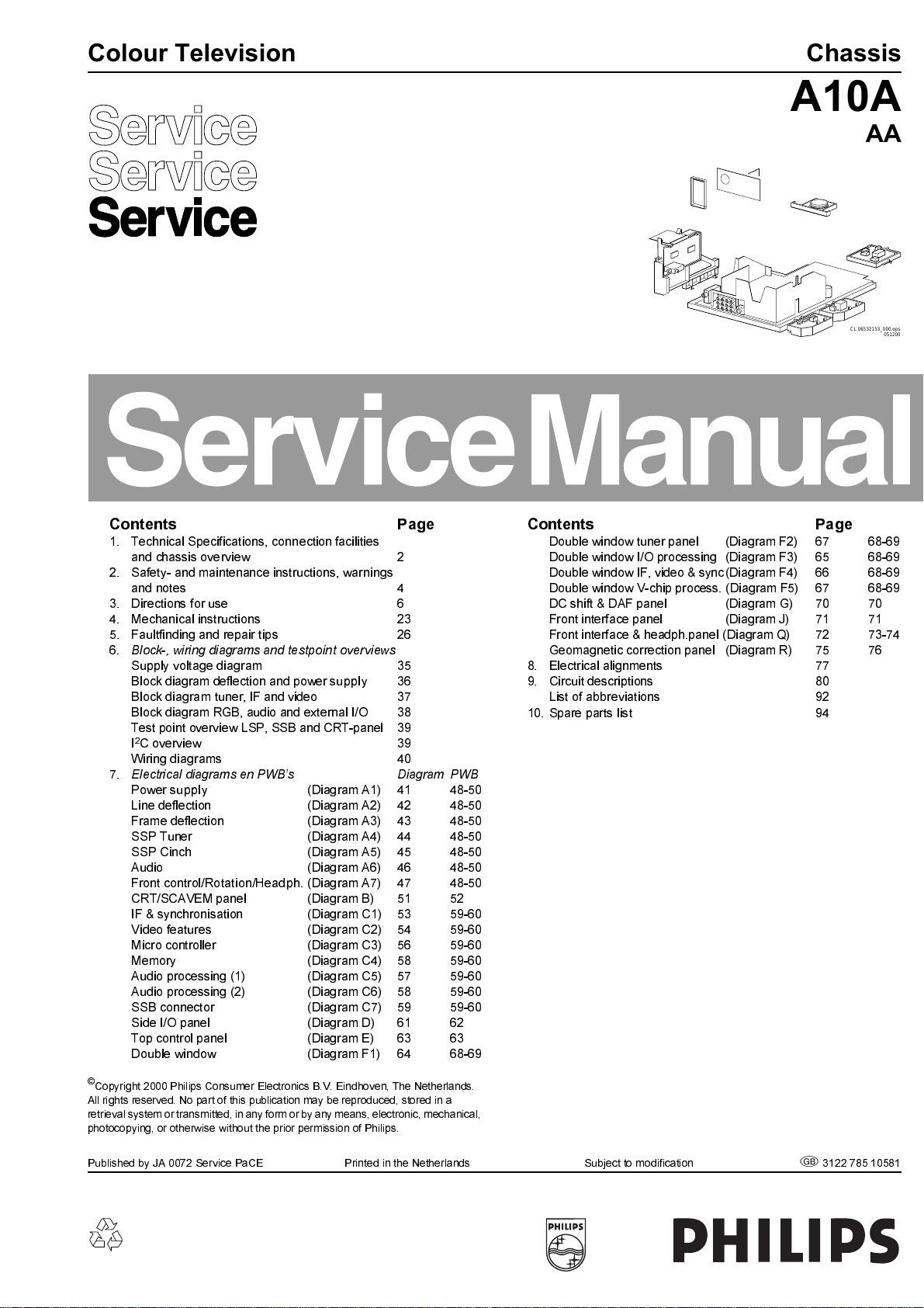
CL 06532153_000.eps
051200
Contents Page Contents Page
1. Technical Specifications, connection facilities
and chassis overview 2
2. Safety- and maintenance instructions, warnings
and notes 4
3. Directions for use 6
4. Mechanical instructions 23
5. Faultfinding and repair tips 26
6.
Block-, wiring diagrams and testpoint overviews
Supply voltage diagram 35
Block diagram deflection and power supply 36
Block diagram tuner, IF and video 37
Block diagram RGB, audio and external I/O 38
Test point overview LSP, SSB and CRT-panel 39
2
C overview 39
I
Wiring diagrams 40
7.
Electrical diagrams en PWB’s Diagram PWB
Power supply (Diagram A1) 41 48-50
Line deflection (Diagram A2) 42 48-50
Frame deflection (Diagram A3) 43 48-50
SSP Tuner (Diagram A4) 44 48-50
SSP Cinch (Diagram A5) 45 48-50
Audio (Diagram A6) 46 48-50
Front control/Rotation/Headph. (Diagram A7) 47 48-50
CRT/SCAVEM panel (Diagram B) 51 52
IF & synchronisation (Diagram C1) 53 59-60
Video features (Diagram C2) 54 59-60
Micro controller (Diagram C3) 56 59-60
Memory (Diagram C4) 58 59-60
Audio processing (1) (Diagram C5) 57 59-60
Audio processing (2) (Diagram C6) 58 59-60
SSB connector (Diagram C7) 59 59-60
Side I/O panel (Diagram D) 61 62
Top control panel (Diagram E) 63 63
Double window (Diagram F1) 64 68-69
©
Copyright 2000 Philips Consumer Electronics B.V. Eindhoven, The Netherlands.
All rights reserved. No part of this publication may be reproduced, stored in a
retrieval system or transmitted, in any form or by any means, electronic, mechanical,
photocopying, or otherwise without the prior permission of Philips.
Double window tuner panel (Diagram F2) 67 68-69
Double window I/O processing (Diagram F3) 65 68-69
Double window IF, video & sync (Diagram F4) 66 68-69
Double window V-chip process. (Diagram F5) 67 68-69
DC shift & DAF panel (Diagram G) 70 70
Front interface panel (Diagram J) 71 71
Front interface & headph.panel (Diagram Q) 72 73-74
Geomagnetic correction panel (Diagram R) 75 76
8. Electrical alignments 77
9. Circuit descriptions 80
List of abbreviations 92
10. Spare parts list 94
Published by JA 0072 Service PaCE Printed in the Netherlands Subject to modification
5
3122 785 10581
Page 2
GB 2 A10A1.
Technical specifications, connection facilities and chassis overview
1.1 Technical specifications
Mains voltage : 90 - 276 Vac
Power consumption : max 160 W
Standby consumption : < 3 W
Mains frequency : 50 - 60 Hz
Tuning system : PLL
Reception : PAL B/G/D/K/I
: SECAM B/G/D/K/
K1
: NTSC M
Sound system : 2CS BG
: NICAM B/G/D/K/I/L
: 2 NICAM BG/D
Sound output : 2 x 5 W
: 2x10W+10W
(Virtual dolby)
Aerial input : Coaxial 75
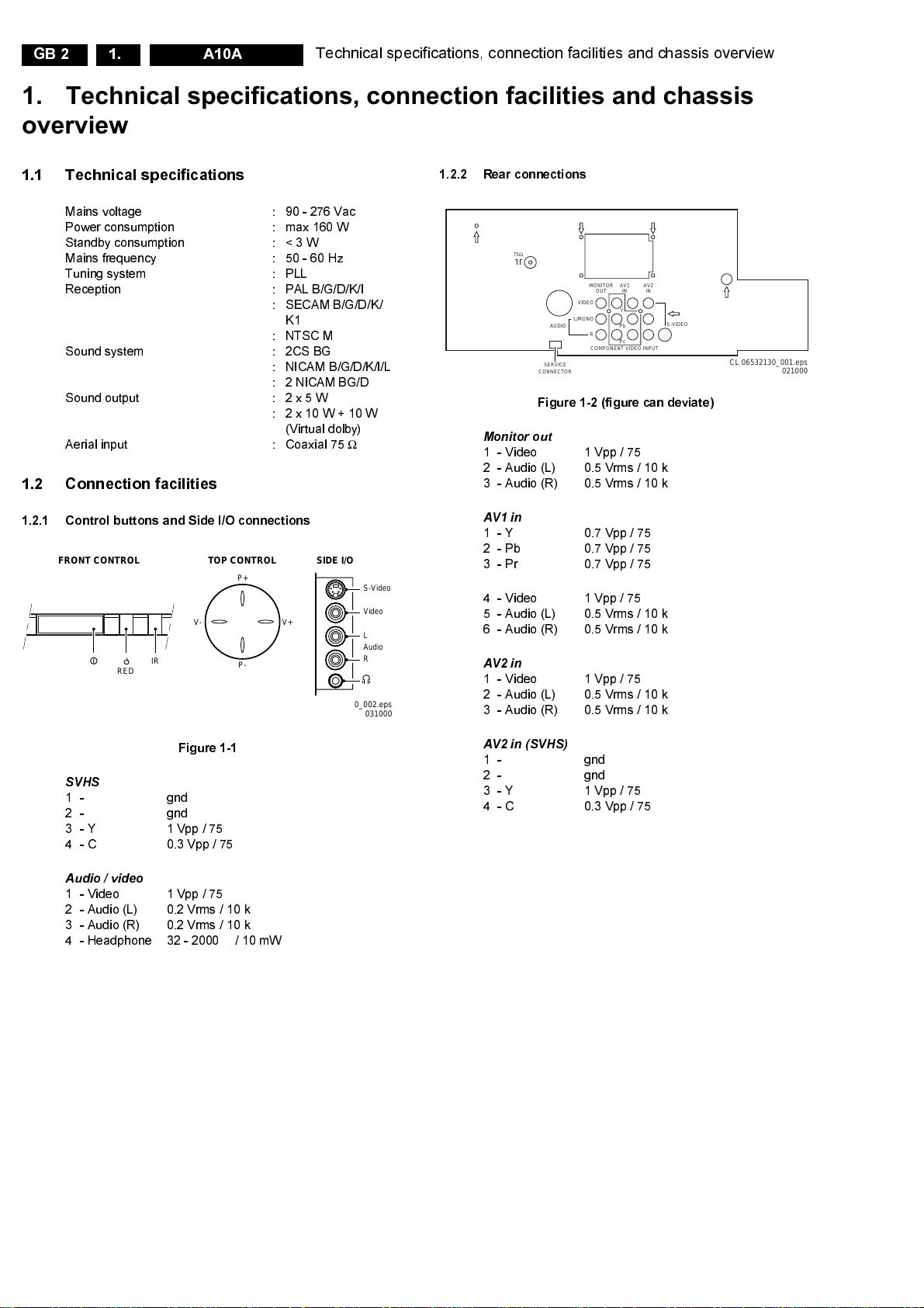
1.2 Connection facilities
1.2.1 Control buttons and Side I/O connections
TOP CONTROL
P+
V+V-
RED
IR
P-
Ω
SIDE I/OFRONT CONTROL
S-Video
Video
L
Audio
R
CL 06532130_002.eps
031000
1.2.2 Rear connections
75Ω
L/MONO
AUDIO
SERVICE
CONNECTOR
Figure 1-2 (figure can deviate)
Monitor out
1 - Video 1 Vpp / 75
2 - Audio (L) 0.5 Vrms / 10 k
3 - Audio (R) 0.5 Vrms / 10 k
AV1 in
1 - Y 0.7 Vpp / 75
2 - Pb 0.7 Vpp / 75
3 - Pr 0.7 Vpp / 75
4 - Video 1 Vpp / 75
5 - Audio (L) 0.5 Vrms / 10 k
6 - Audio (R) 0.5 Vrms / 10 k
AV2 in
1 - Video 1 Vpp / 75
2 - Audio (L) 0.5 Vrms / 10 k
3 - Audio (R) 0.5 Vrms / 10 k
MONITOR
AV1
OUT
VIDEO
Y
Pb
R
Pc
COMPONENT VIDEO INPUT
AV2
IN
IN
S-VIDEO
CL 06532130_001.eps
Ω
Ω
Ω
Ω
Ω
Ω
Ω
Ω
Ω
Ω
Ω
Ω
021000
kq
kq
kq
jq
jq
jq
jq
jq
jq
jq
jq
jq
Figure 1-1
SVHS
1 - gnd
2 - gnd
3 -Y 1Vpp/75
4 -C 0.3Vpp/75
Ω
Ω
Audio / video
1 - Video 1 Vpp / 75
2 - Audio (L) 0.2 Vrms / 10 k
3 - Audio (R) 0.2 Vrms / 10 k
Ω
Ω
Ω
4 - Headphone 32 - 2000Ω/10mW
v
v
j
j
jq
jq
jq
rt
AV2 in (SVHS)
1 - gnd
2 - gnd
3-Y 1Vpp/75
4 - C 0.3 Vpp / 75
v
v
Ω
Ω
j
j
Page 3
Technical specifications, connection facilities and chassis overview
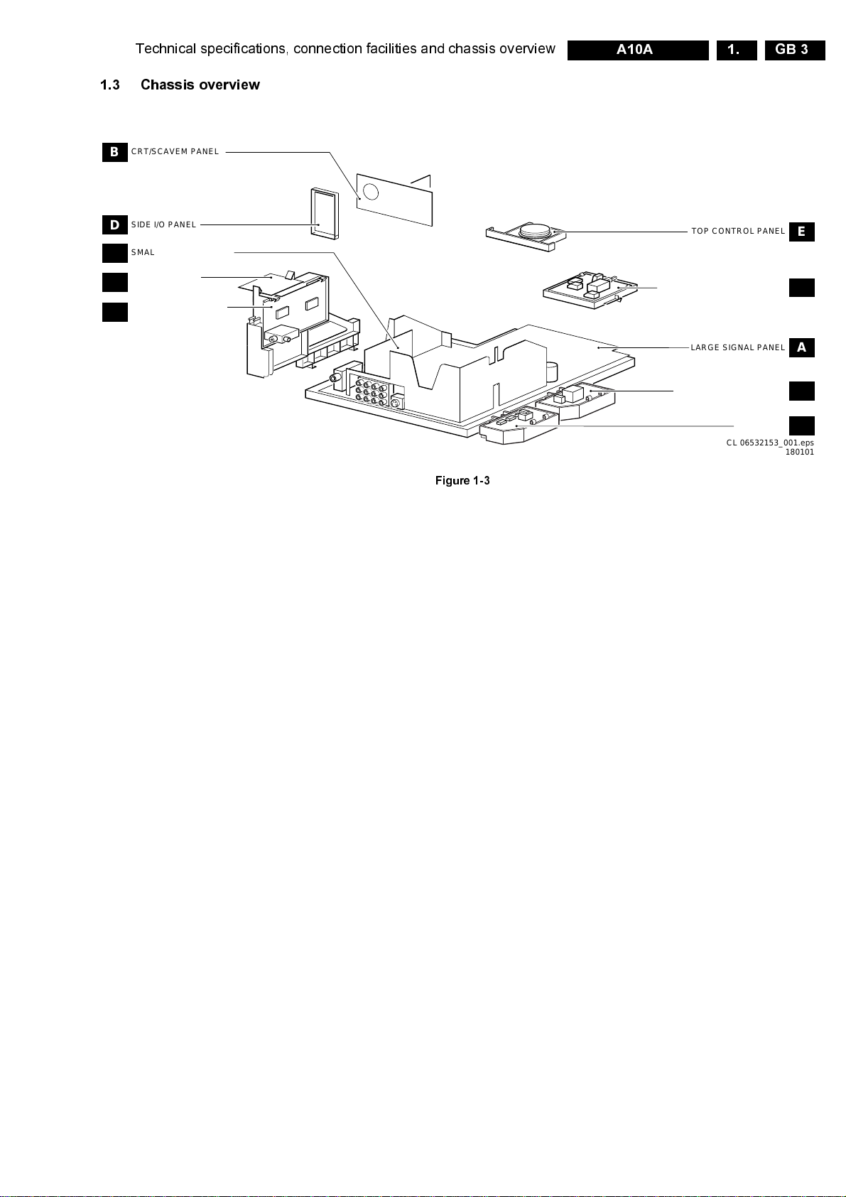
1.3 Chassis overview
CRT/SCAVEM PANEL
B
SIDE I/O PANEL
D
SMALL SIGNAL BOARD
C
GEOMAGNETIC
R
CORRECTION PANEL
PIP/DOUBLE WINDOW
F
PANEL
TOP CONTROL PANEL
MAINS SWITCH PANEL/
FRONT INTERFACE PANEL
GB 3A10A 1.
E
J/Q
Figure 1-3
LARGE SIGNAL PANEL
MAINS HARMONIC PANEL
DAF PANEL
CL 06532153_001.eps
A
M
G
180101
Page 4
GB 4 A10A2.
Safety- & maintenance instructions, warnings and notes
2.1 Safety instructions for repairs
Safety regulations require that during a repair:
• Safety components, indicated by the symbol
be replaced by components identical to the original ones;
• When replacing the CRT, safety goggles must be worn.
Safety regulations require that after a repair, the set must be
returned in its original condition. In particular attention should
be paid to the following points:
• General repair instruction: as a strict precaution, we
advise you to resolder the solder joints, through which
the horizontal deflection current is flowing, in particular:
– All pins of the line output transformer (LOT);
– Fly-back capacitor(s);
– S-correction capacitor(s);
– Line output transistor;
– Pins of the connector with wires to the deflection coil;
– Other components through which the deflection
current flows.
Note: Thisresoldering is advised to prevent bad connections
due to metal fatigue in solder joints and is therefore only
necessary for television sets older than 2 years.
• The wire trees and EHT cable should be routed correctly
and fixed with the mounted cable clamps.
• The insulation of the mains lead should be checked for
external damage.
• The mains lead strain relief should be checked for its
function in order to avoid touching the CRT, hot
components or heat sinks.
• The electricalDCresistance between the mains plug and
the secondary side should be checked (only for sets
which have a mains isolated power supply). This check
can be done as follows:
– Unplug the mains cord and connect a wire between
the two pins of the mains plug;
– Set the mains switch to the 'ON' position (keep the
mains cord unplugged!);
– Measure the resistance value between the pins of
the mains plug and the metal shielding of the tuner or
the aerial connection on the set. The reading should
be between 4.5 MΩand 12 MΩ.
– Switch off the TV and remove the wire between the
two pins of the mains plug.
• The cabinet should be checked for defects to avoid
touching of any inner parts by the customer.
2.2 Maintenance instructions
, should
h
2.3 Warnings
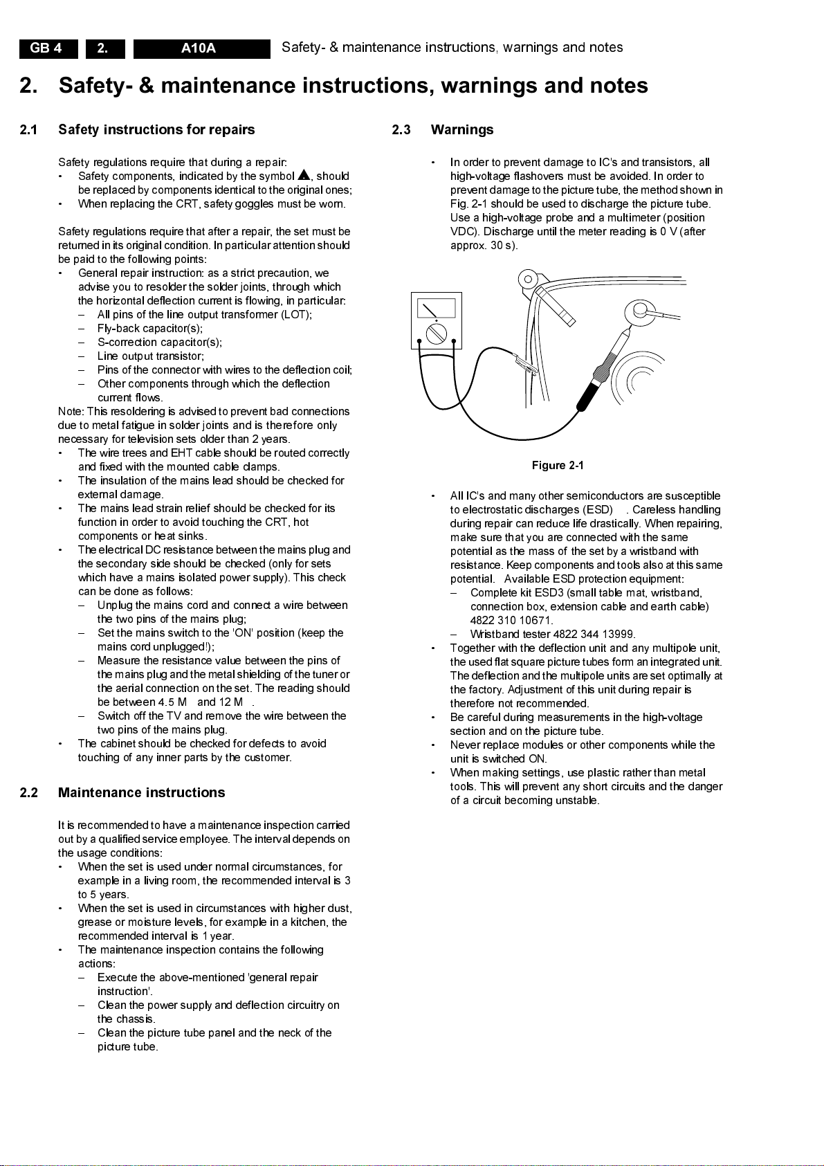
• In order to prevent damage to IC's and transistors, all
high-voltage flashovers must be avoided. In order to
prevent damage to the picture tube, the method shown in
Fig. 2-1 should be used to discharge the picture tube.
Use a high-voltage probe and a multimeter (position
VDC). Discharge until the meter reading is 0 V (after
approx. 30 s).
V
Figure 2-1
• All IC's and many other semiconductors are susceptible
to electrostatic discharges (ESD)
during repair can reduce life drastically. When repairing,
make sure that you are connected with the same
potential as the mass of the set by a wristband with
resistance. Keep components and tools also at this same
potential. Available ESD protection equipment:
– Complete kit ESD3 (small table mat, wristband,
connection box, extension cable and earth cable)
4822 310 10671.
– Wristband tester 4822 344 13999.
• Together with the deflection unit and any multipole unit,
the used flat square picture tubes form an integrated unit.
The deflection and the multipole units are set optimally at
the factory. Adjustment of this unit during repair is
therefore not recommended.
• Be careful during measurements in the high-voltage
section and on the picture tube.
• Never replace modules or other components while the
unit is switched ON.
• When making settings, use plastic rather than metal
tools. This will prevent any short circuits and the danger
of a circuit becoming unstable.
. Careless handling
w
CL 26532098/042
140792
It is recommended to have a maintenance inspection carried
out by a qualified service employee. The intervaldepends on
the usage conditions:
• When the set is used under normal circumstances, for
example in a living room, the recommended interval is 3
to 5 years.
• When the set is used in circumstances with higher dust,
grease or moisture levels, for example in a kitchen, the
recommended interval is 1 year.
• The maintenance inspection contains the following
actions:
– Execute the above-mentioned 'general repair
instruction'.
– Clean the power supply and deflection circuitry on
the chassis.
– Clean the picture tube panel and the neck of the
picture tube.
Page 5
2.4 Notes
Safety- & maintenance instructions, warnings and notes
GB 5A10A 2.
• The direct voltages and oscillograms should be
measured with regard to the tuner earth (
) as this is called.
I
(
• The direct voltages and oscillograms shown in the
diagrams are indicative and should be measured in the
Service Default Mode (see chapter 5) with a colour bar
signal and stereo sound (L: 3 kHz,R:1 kHz unless stated
otherwise) and picture carrier at 475. 25 M H z .
• Where necessary, the oscillograms and direct voltages
are measured with (
Voltages in the power supply section are measuredboth
for normal operation (
values are indicated by means of the appropriate
symbols.
• The picture tube PWB has printed spark gaps. Each
spark gap is connected between an electrode of the
picture tube and the Aquadag coating.
• The semiconductors indicated in the circuit diagram and
in the parts lists are completely interchangeable per
position with the semiconductors in the unit, irrespective
of the type indication on these semiconductors.
• DOLBY, the double D symbol and PRO LOGIC are
trademarks of Dolby Laboratories Licensing Corporation.
Manufactured under license from Dolby Laboratories
Licensing Corporation.
) and without (E) aerial signal.
D
) and in Standby (F). These
G
), or hot earth
H
Page 6
GB 6 A10A3.
2
I
NTRODUCTION
Thank you for purchasing this televison set. You are now the proud owner of a PHILIPS TV
set which promises full value to you as a customer. Please read the instruction manual carefully
and thoroughly to help you install and operate your TV set.
T
ABLE OF
C
ONTENTS
S
AFETY
I
NFORMATION
/U
SEFUL
T
IPS ...........................................................................
3
B
EFORE
C
ALLING
S
ERVICE ...................................................................................................
3
I
NSTALLATION ...............................................................................................................................
4
C
ONNECTING THE
A
UDIO
/V
IDEO
S
OCKETS
Playback ....................................................................................................................................................
5
Recording .................................................................................................................................................
7
F
UNCTIONS OF
R
EMOTE
C
ONTROL .............................................................................
8
F
UNCTIONS OF
TV
C
ONTROLS .......................................................................................
10
S
ELECTING THE
M
ENU
L
ANGUAGE AND
A
UTOMATIC
T
UNING
OF
C
HANNELS ...............................................................................................................................
11
M
ANUAL
T
UNING OF
C
HANNELS ..................................................................................
12
S
ELECTING THE
C
OLOUR
/S
OUND
S
YSTEM .............................................................
13
F
INE
T
UNING OF
C
HANNELS ............................................................................................
14
S
ORTING OF
C
HANNELS ........................................................................................................
15
E
DITING OF
C
HANNELS .........................................................................................................
16
N
AMING OF
C
HANNELS .........................................................................................................
17
U
SING THE
P
ICTURE
/S
OUND
M
ENU..............................................................................
18
A
CTIVATING THE
T
IMER .........................................................................................................
19
A
CTIVATING THE
C
HILD
L
OCK
Access Code ...........................................................................................................................................
21
Change Code .........................................................................................................................................
22
Lock Channel .........................................................................................................................................
23
Clear All ...................................................................................................................................................
24
U
SING THE
S
URF
C
ONTROL ..............................................................................................
25
U
SING THE
S
CREEN
F
ORMAT ............................................................................................
26
A
CTIVATING THE
B
LUE
M
UTE
C
ONTROL ...............................................................
27
U
SING THE
P
ROGRAMME
L
ISTING
C
ONTROL .....................................................
27
S
MART
P
ICTURE AND
S
MART
S
OUND .........................................................................
28
A
CTIVATING THE
PIP (P
ICTURE-IN-
P
ICTURE
)
AND
D
OUBLE
W
INDOW
C
ONTROL .............................................................................
29
U
SING THE
T
ELETEXT...............................................................................................................
32
S
PECIFICATIONS ...........................................................................................................................
34
!
Directions for use
29" / 34"
Colour Television
Instructions for use
29PT6361
34PT6361
3139 125 28001
Page 7
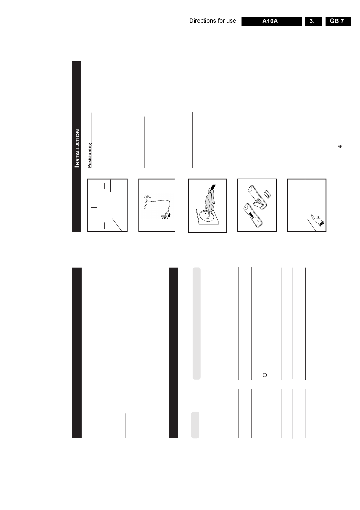
Directions for use
4
I
NSTALLATION
Positioning of the TV set
• Place your TV set on a solid base, strong enough to
withstand the weight of the set.
• Leave a space of at least 5 cmaround each side of the
TV set to allow for proper ventilation.
• Do not place TV set near a radiator or other sources of
heat.
• Do not place TV set where it can be exposed to rain or
excesssive moisture.
Connecting the Aerial
• Insert the aerial plug into the socket ¬ at the rear of
the set.
Connecting to the mains
• Insert the mains plug into the wall socket. (For correct
mains voltage, refer to the type sticker at the rear of the
set).
Note : This diagram is not representative of the actual
plug and socket.
Using the Remote Control
• Insert the correct type of batteries into the compartment.
• Ensure the batteries are placed in the right direction.
Note : Remove the batteries from the remote
control handset if handset is not used for a long time.
Switching on the TV set
• Press the mains power button to switch on/off the TV set.
• If the set is on standby mode (indicator light is red), press
the Standby button on the remote control to switch on set.
5 cm
5 cm
5 cm
ÉÑ
ÉÑ
ÉÑ
GB 7A10A 3.
IPS
T
SEFUL
/U
NFORMATION
I
AFETY
S
Safety
Disconnect mains plug when :
leather or soft cloth.
– the red light below the TV screen is flashing continuously.
– a bright white line is displayed across the screen.
– cleaning the TV screen. Never use abrasive cleaning agents. Use a slight damp chamois
– there is a lightning storm.
– the set is left unattended for a prolonged period of time.
Useful Tips
• Do not place your TV set under direct sunlight or heat.
ERVICE
S
ALLING
C
EFORE
B
or water.
• Avoid placing your set (e.g. near the window) where it is likely to be exposed to rain
to allow it to be demagnetised. A demagnetised set supports good picture quality.
some parts of the screen may occur.
• Do not leave your set on standby mode for a prolonged period of time. Switch off set
• Do not shift or move the set around when it is switched on. Uneveness in colour in
• Never attempt to repair a defective TV yourself. Always consult a skilled service personnel.
Symptom What you should do
Below is a list of frequently occurred symptoms. Before you call for dservice, make these simple
checks. Some of these symptoms can easily be rectified if you know what to do.
Colour patch • Switch off the TV by the mains power button. Wait for 20
socket. If there is still no power, disconnect plug. Wait for
60 seconds and re-insert plug. Switch on the TV again.
objects.
• Check the TV is not placed too near speakers or magnetic
No power • Check the TV’s AC power cord is plugged into the mains
(uneveness) minutes before switching on again.
• Possible TV station problem. Try another channel.
No picture • Check the antenna connection at the rear of the TV.
Good picture • Try increasing the volume.
but no sound • Check that the sound is not muted. If it is muted, press the
HH
HH
H
(mute) button on the remote control to restore sound.
cleaner, etc. Switch off appliances.
“Ghost” images directional antenna may improve reception.
Good sound but poor • Try increasing the contrast and brightness setting.
colour or no picture
Snowish picture and • Check antenna connection at the rear of the TV.
noise
Horizontal dotted lines • Possible electrical interference e.g. hairdryer, vacuum
TV not responding to • Check life span of batteries of remote control handset.
Double images or • Possible poor positioning of antenna. Using a highly
3
sensor lens on the TV.
remote control handset • Aim remote control handset directly at remote control
Page 8
GB 8 A10A3.
6
C
ONNECTING THE
A
UDIO
/V
IDEO
S
OCKETS
(P
LAYBACK
)
For more convenient direct playback connections, the Side Audio/Video Input sockets allow for quick
and easy connections, particularly Camcorder tape recordings.
– Connect the S-VIDEO socket (if available) from the Camcorder to the Side S-VIDEO
socket of the TV. You need not connect the Side VIDEO IN socket of the TV if the
S-VIDEO socket is connected.
– Connect the AUDIO OUT sockets (Right and Left) from the Camcorder to the Side
AUDIO IN sockets.
You can view the playback of DVD discs by using the COMPONENT VIDEO INPUT sockets on the
rear of the TV.
– Connect the “Y”, “Pb” and the “Pr” INPUT sockets on the TV to the “Y”, “Pb” and
“Pr” OUTPUT sockets on the DVD to view playback of DVD discs.
Connect headphone jack to
socket for personal listening
Camcorder
AV sockets
on rear of
TV
Back of DVD
DVD (Equipped with “Y”,
“Pb” and “Pr” and Output
sockets)
L/Mono
R
S-VIDEO
VIDEO
AUDIO
AV1 in AV2 inMonitor out
COMPONENT VIDEO INPUT
Y
Pb
Pr
OUT
AUDIO
Y
L
OUT
R
Pb
Pr
Directions for use
)
LAYBACK
(P
AV sockets
on rear of
OCKETS
S
TV
S-VIDEO
IDEO
/V
UDIO
A
AV1 in AV2 inMonitor out
Pr
Pb
Y
COMPONENT VIDEO INPUT
R
VIDEO
L/Mono
AUDIO
ONNECTING THE
C
AV sockets
on rear of
AV1 in AV2 inMonitor out
VIDEO
TV
S-VIDEO
Pb
Y
L/Mono
AUDIO
Pr
COMPONENT VIDEO INPUT
R
Back of
VCR
CR (Equipped with
V
Video and Audio Output
L
AUDIO
R
OUT
VIDEO
OUT
OUT
ANTENNA
sockets
IN
IN
IN
VIDEO OUT sockets on the VCR.
You can view the playback of VCR tapes (Video Disc players, camcorders, etc.) by using the AUDIO
and VIDEO INPUT sockets on the rear of the TV.
– Connect the VIDEO and AUDIO IN sockets on the rear of the TV to the AUDIO and
Back of S-VHS VCR
IN
OUT
ANTENNA
OUT
S-VIDEO
IN
OUT
VIDEO
L
IN
OUT
AUDIO
R
The S-Video connection on the rear of the TV is used for the playback of S-VHS VCR tapes, Video
Discs, Video Games or Compact Disc-Interactive (cd-i) discs. Better picture detail and clarity is
possible with the S-Video playback as compared to the picture from a normal antenna (RF)
S-VHS VCR.
connection.
– Connect the S-VIDEO socket on the rear of the TV to the S-VHS OUT socket on a
– Connect the AUDIO IN sockets from the rear of the TV to the AUDIO OUT sockets
on the VCR.
connected.
Note : You need not connect the VIDEO IN socket of the TV if S-VIDEO IN socket is
5
Page 9
Directions for use
8
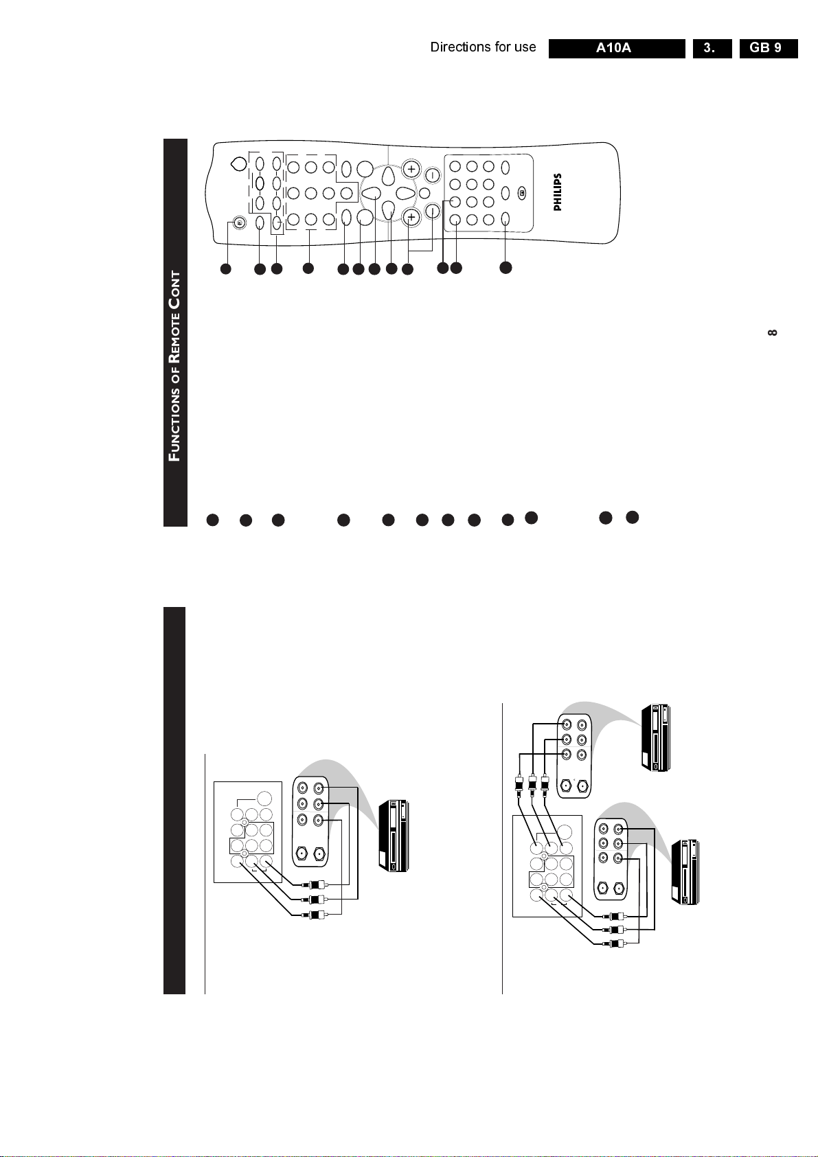
F
UNCTIONS
OF
R
EMOTE
C
ONTROL
1
2
3
4
5
6
7
8
9
10
11
e
A/CH
4m
MENU
SURF
SMARTSMART
±
`
n
o
r
vp
A
CH
H
\
5
13
2
4
6
7
9
8
0
INDEX
AV
INCR. SURR. INCREDIBLE
OK
bhfy
2
PIP
`
PIP CH
UP DN
12
1 SLEEPTIMER
Allows you to select a time period after which the
set will switch to standby mode automatically.
2 A/CH (Alternate Channel)
Allows you to alternate between the last
viewed channel and the present channel.
3
PIP ON/OFF (Picture-in-Picture On/Off)
Allows you to access the Picture-in-Picture and
Double Window features. (For more detailed
description of functions, refer to the sections
on “Activating the PIP and Double Window
Control”)
4 DIGIT (0 -9)
Allows you select a channel. Note : For a 2-digit
number, the second digit must be entered before
the “–” sign disappears.
5 SMART SOUND
Allows you to select your desired sound setting
from 4 types of sound settings.
6 MENU
Displays main menu. Also exits menu from screen.
7 CURSOR UP
Allows you to select the next item on the menu.
8 CURSOR LEFT
Allows you to access the sub-menus and adjust
the settings.
9 VOLUME + / –
Increases or decreases volume.
10 OSD
– Displays the channel number, sound and colour
transmission mode, status of the sleeptimer.,
channel name (if channel is named) and the
current time (if current time is being entered in
the Timer menu).
– Also allows you to exit menu from screen.
11 AV
Allows you to select the AV channels.
12 INCREDIBLE SURROUND
– Allows you to select Incredible Surround/Virtual
Dolby surround sound when transmission is in
stereo mode. Virtual Dolby Surround allows you
to enjoy the sensation of Home Cinema surround
sound with just 2 front speakers.
– Allows you to select Spatial Sound when
transmission is in mono mode.
GB 9A10A 3.
)
VCR (Equipped with
Video and Audio
ECORDING
(R
OCKETS
S
IDEO
/V
UDIO
A
AV1 in AV2 inMonitor out
AV sockets
on rear of
Y
VIDEO
L/Mono
ONNECTING THE
C
Connection for recording from the TV channel
TV
S-VIDEO
Pb
AUDIO
Pr
R
OUT
OUT
COMPONENT VIDEO INPUT
OUT
L
AUDIO
R
VIDEO
ANTENNA
IN
IN
IN
VCR (Equipped with Video
and Audio Input sockets
sockets on the rear of the TV.
audio system instead of the VCR. For mono equipment, connect only the AUDIO L socket.
– Connect the corresponding INPUT sockets of the VCR to the MONITOR OUTPUT
– To enhance the sound of your TV, connect the AUDIO L and R sockets to an external
Connection for recording from one VCR to another VCR
AV1 in AV2 inMonitor out
AV sockets on
Back of
VCR
L
OUT
AUDIO
R
OUT
VIDEO
IN
OUT
ANTENNA
Pr
COMPONENT VIDEO INPUT
L
AUDIO
OUT
R
VIDEO
OUT
OUT
ANTENNA
S-VIDEO
Pb
Y
R
VIDEO
L/Mono
AUDIO
rear of TV
Output sockets
VCR 2
VCR (Equipped with Video
IN
IN
IN
and Audio Input sockets
VCR 1
sockets at either AV1 or AV2. .
– Connect the sockets of the VCR which you wish to record from, to the corresponding
rear of the TV.
– Connect the sockets of the receiving VCR to the MONITOR OUTPUT sockets on the
7
Page 10
GB 10 A10A3.
10
F
UNCTIONS OF
TV
C
ONTROLS
➩
1
2
3
➩
4
5
6
7
A
A
A
A
A
A
1 Mains Power button Switch mains power on or off.
2 Standby Light indicator Indicate red light when standby mode is activated.
3 Remote Sensor Acts as a sensor for activating the controls of the TV
when remote control handset is aimed at it.
4 Volume button Adjust sound volume softer.
5 Volume button Adjust sound volume louder.
6 Programme button Select channel in ascending order.
7 Programme button Select channel in descending order.
Note
• You can enter the main menu by pressing both
the Volume and buttons at the same time.
• Press the Programme or button to select the
next item on the menu.
• Press the Volume or button to access the
sub-menus and adjust the settings.
Directions for use
ONTROL
C
EMOTE
R
UNCTIONS OF
F
(The red light indicator lights up when set is
on standby mode).
Channel Up/Down, Digit (0 -9) or Standby button.
Allows you to select your desired picture setting
from 5 types of picture settings.
Allows you to select up to a maximum of 10
– Switch set off temporarily to standby mode.
13 STANDBY
– To switch on set from standby mode, press
14 SMART PICTURE
15 SURF
13
r
2
PIP CH
o
PIP
n
A/CH
6
UP DN
2
5
4
13
vp
channels and view quickly the selected channels.
Allows you to access the sub-menus and adjust
the settings.
Allows you to select the next item on the menu.
16 CURSOR RIGHT
17 CURSOR DOWN
18 CHANNEL + / –
17
15
14
16
9
`
SURF
SMARTSMART
8
0
±
MENU
7
Selects channel in ascending or descending order.
18
Mutes sound. To restore sound, press button
19 MUTE
19
CH
H
A
INDEX
again.
44
44
another channel at a specified time while you
are watching nother channel or when the set
is on standby mode.
4
Allows you to switch from Stereo to Mono
sound during stereo transmission or to choose
between language5or language6during dual
sound transmission.
21
24
23
22
`
OK
e
bhfy
INCR. SURR. INCREDIBLE
20
\
4m
AV
Allows you to set the clock to switch to
20 TIMER
21
Allows you to access teletext information.
(For detailed description of functions, refer
to section on “Using the Teletext”
22 TELETEXT
Allows you to view a more vivid and realistic
picture with better contrast when the “ON”
function is selected.
Allows you to navigate through a list of installed
programmes for a quick overview of the channels
and activate the channel you have selected.
23 INCREDIBLE PICTURE
24 PROGRAMME LIST
9
Page 11
Directions for use
12
M
ANUAL
T
UNING OF
C
HANNELS
Manual tuning allows you to store each programme manually.
1. Enter main menu.
2. Press button repeatedly
until INSTALL is
selected.
3. Enter INSTALL menu.
4. Press button repeatedly
until MANUAL STORE
is selected.
5. Enter MANUAL STORE
menu.
6. Select SEARCH.
7. Start manual tuning of
channel. Searching stops
once a transmitting
channel is found.
8. Select CHANNEL.
9. Key in the desired channel
number.
10. Select STORE.
11. Store tuned channel.
Note : If you want to
continue searching for
another transmitting
channel, repeat steps
7 to 11.
12. Exit menu from screen.
Press button
Result on TV Screen
•
PICTURE
LANGUAGE
•
SOUND
AUTO STORE
•
FEATURES
MANUAL STORE
•
INSTALL
SORT
CHANNEL EDIT
É
▲
MENU
5
13
2
4
6
7
9
8
0
m
e
A/CH
4m
MENU
SURF
SMARTSMART
±
`
n
o
r
vp
A
CH
H
\
5
13
2
4
6
7
9
8
0
INDEX
AV
INCR. SURR. INCREDIBLE
OK
bhfy
2
PIP
`
PIP CH
UP DN
INSTALL
•
LANGUAGE
COLOUR SYSTEM
•
AUTO STORE
SOUND SYSTEM
•
MANUAL STORE
SEARCH
•
SORT
CHANNEL
•
CHANNEL EDIT
STORE
•
▲É▼
▼
▲
Ñ
INSTALL
MANUAL STORE
•
COLOUR SYSTEM
•
SOUND SYSTEM
SEARCH
•
048.31MHZ
•
CHANNEL
•
STORE
É
▼
▲
Ñ
INSTALL
MANUAL STORE
•
COLOUR SYSTEM
•
SOUND SYSTEM
SEARCH
•
196.25MHZ
•
CHANNEL
•
STORE
É
▼
▲
Ñ
INSTALL
MANUAL STORE
•
COLOUR SYSTEM
•
SOUND SYSTEM
•
SEARCH
•
CHANNEL
STORE
•
STORED
É
▼
▲
Ñ
INSTALL
MANUAL STORE
•
COLOUR SYSTEM
•
SOUND SYSTEM
SEARCH
•
196.25MHZ
•
CHANNEL
•
STORE
É
▲
COLOUR SYSTEM
SOUND SYSTEM
•
•
INSTALL
MANUAL STORE
18
É
▼
•
CHANNEL
STORE
SEARCH
Ñ
•
•
GB 11A10A 3.
10
HANNELS
C
ANGUAGE
L
UNING OF
ENU
T
M
UTOMATIC
A
ELECTING THE
S
AND
Result on TV Screen
Press button
Before you tune in the channels by the Auto Store method, select the menu language of your
choice.
SHARPNESS
BRIGHTNESS
COLOUR
CONTRAST
PICTURE
SOUND
FEATURES
INSTALL
É
▼
•
•
•
•
1. Enter main menu.
MENU
r
2
PIP CH
UP DN
o
PIP
n
vp
A/CH
COLOUR TEMP
LANGUAGE
AUTO STORE
MANUAL STORE
PICTURE
SOUND
FEATURES
•
•
•
until INSTALL is
selected.
SORT
CHANNEL EDIT
INSTALL
É
▲
•
2. Press button repeatedly
6
9
`
SURF
SMARTSMART
2
5
8
0
±
MENU
7
4
13
ENGLISH
É
▲
•
LANGUAGE
AUTO STORE B.MELAYU
Ñ
•
INSTALL
3. Enter INSTALL menu.
CH
H
A
▼
MANUAL STORE
SORT
CHANNEL EDIT
•
•
•
INSTALL
4. Enter LANGUAGE mode.
\
4m
INDEX
AV
ENGLISH
É
▲
•
LANGUAGE
Ñ
bhfy
INCR. SURR. INCREDIBLE
AUTO STORE B.MELAYU
•
`
OK
e
▼
MANUAL STORE
SORT
CHANNEL EDIT
•
•
•
•
INSTALL
5. Select desired language.
OR
ENGLISH
É
▲
Ñ
6. Exit from language mode.
•
LANGUAGE
AUTO STORE B.MELAYU
MANUAL STORE
SORT
CHANNEL EDIT
•
•
•
•
▼
▲
LANGUAGE
•
INSTALL
7. Select AUTO STORE.
SEARCH
É
▼
•
▲
MANUAL STORE
AUTO STORE
SORT
CHANNEL EDIT
Ñ
•
•
•
•
INSTALL
PLEASE WAIT
CHAN.FOUND 8
SEARCHING
É
•
LANGUAGE
AUTO STORE
MANUAL STORE
SORT
CHANNEL EDIT 048.31 MHZ
•
•
•
•
•
9. Start automatic tuning.
8. Enter AUTO store mode.
▼
•
SEARCH
É
▲
LANGUAGE
•
INSTALL
▼
•
MANUAL STORE
AUTO STORE
SORT
CHANNEL EDIT
Ñ
•
•
•
•
exit menu from screen.
10. When tuning is completed,
m
11
Page 12
GB 12 A10A3.
14
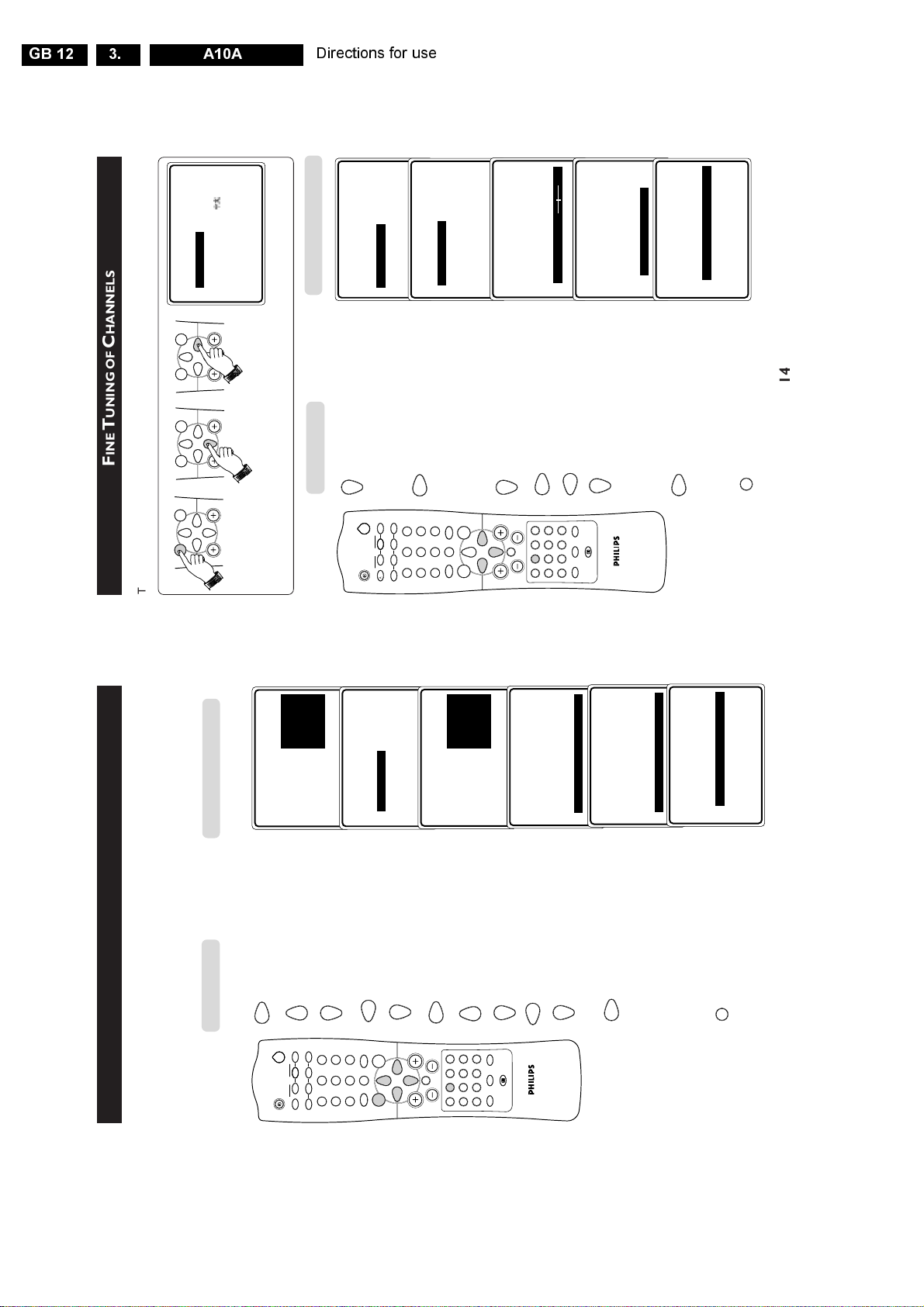
F
INE
T
UNING OF
C
HANNELS
This feature allows you to adjust picture reception in areas of weak reception.
1. Enter main menu. 2. Select INSTALL. 3. Enter install menu.
4. Press button repeatedly
until MANUAL STORE
is selected.
5. Enter MANUAL STORE
menu.
6. Press button repeatedly until
FINE TUNE is selected.
7. Start fine-tuning until desired
picture and sound is obtained.
8. Select STORE.
9. Store last fine-tuned status.
10. Exit menu from screen.
Press button
➠
➠
MENU
SURF
MENU
SURF
MENU
SURF
➠
e
A/CH
4m
MENU
SURF
SMARTSMART
±
`
n
o
r
vp
A
CH
H
\
5
13
2
4
6
7
9
8
0
INDEX
AV
INCR. SURR. INCREDIBLE
OK
bhfy
2
PIP
`
PIP CH
UP DN
m
INSTALL
•
LANGUAGE
COLOUR SYSTEM
•
AUTO STORE
SOUND SYSTEM
•
MANUAL STORE
SEARCH
•
SORT
CHANNEL
•
CHANNEL EDIT
STORE
•
▲É▼
▼
▲
É
INSTALL
MANUAL STORE
COLOUR SYSTEM
•
AUTO
•
SOUND SYSTEM PAL-SECAM
•
SEARCH NTSC
•
CHANNEL
•
STORE
Ñ
INSTALL
LANGUAGE
•
ENGLISH
•
AUTO STORE B.MELAYU
•
MANUAL STORE
•
SORT
•
CHANNEL EDIT
Ñ
▲
É
▼
▼
▲
INSTALL
MANUAL STORE
•
SOUND SYSTEM
•
SEARCH
•
CHANNEL
•
STORE
FINE TUNE
Ñ
É
▼
▲
Ñ
INSTALL
MANUAL STORE
COLOUR SYSTEM
•
SOUND SYSTEM
•
SEARCH
•
CHANNEL
STORE
•
É
▼
▲
Ñ
INSTALL
MANUAL STORE
•
COLOUR SYSTEM
•
SOUND SYSTEM
SEARCH
•
048.31MHZ
•
CHANNEL
•
STORE
É
OR
Directions for use
Result on TV Screen
YSTEM
S
OUND
/S
OLOUR
C
ELECTING THE
S
Result on TV Screen
Press button
This feature allows you to select your desired COLOUR and SOUND system. If AUTO
is selected, the respective colour and sound system will be automatically selected according
to the transmission system.
Note : Select another colour and sound system if reception is poor at AUTO mode.
Repeat step 1 to step 5 as in “MANUAL TUNING OF CHANNELS”
AUTO
É
▲
•
SOUND SYSTEM PAL
COLOUR SYSTEM
Ñ
•
INSTALL
MANUAL STORE
selected. Enter COLOUR
SYSTEM mode.
6. COLOUR SYSTEM is
r
2
o
PIP
n
A/CH
▼
SEARCH SECAM
CHANNEL NTSC 3.58
STORE NTSC 4.43
•
•
•
•
system.
7. Select the desired colour
OR
6
PIP CH
UP DN
2
5
4
13
vp
AUTO
B/G
É
▲
•
COLOUR SYSTEM
SEARCH D/K
CHANNEL I
STORE M
SOUND SYSTEM
Ñ
•
•
•
•
MANUAL STORE
mode.
SOUND SYSTEM.
8. Exit from colour system
9. Proceed to select
`
SURF
0
±
MENU
9
8
INSTALL
SMARTSMART
7
▼
•
CH
H
A
AUTO
É
▲
•
COLOUR SYSTEM
SOUND SYSTEM B/G
Ñ
•
INSTALL
MANUAL STORE
mode.
10. Enter SOUND SYSTEM
\
4m
INDEX
AV
SEARCH D/K
CHANNEL I
STORE M
•
•
•
11. Select the desired sound
▼
•
system.
▲
INSTALL
MANUAL STORE
12. Exit from sound system
OR
`
OK
e
bhfy
INCR. SURR. INCREDIBLE
É
•
STORE
CHANNEL
SOUND SYSTEM
SEARCH
COLOUR SYSTEM
Ñ
•
•
•
mode.
until STORE is selected.
13. Press button repeatedly
▲
▼
CHANNEL
SOUND SYSTEM
SEARCH
COLOUR SYSTEM
•
•
•
INSTALL
MANUAL STORE
13. Store selected systems.
STORED
É
▼
▲
•
STORE
COLOUR SYSTEM
Ñ
•
INSTALL
MANUAL STORE
048.31MHZ
É
▼
•
SEARCH
SOUND SYSTEM
CHANNEL
STORE
Ñ
•
•
•
14. Exit menu from screen.
m
13
Page 13
Directions for use
16
E
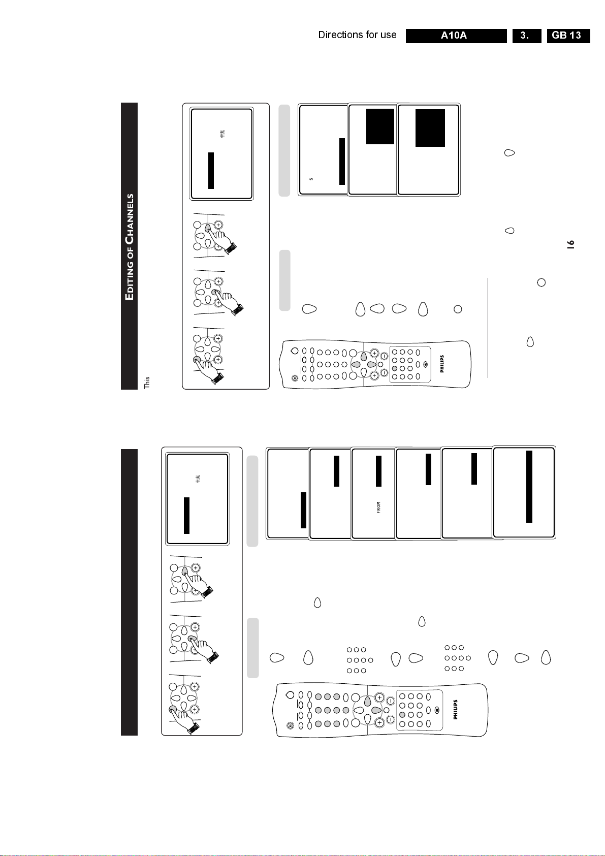
DITING OF
C
HANNELS
This feature allows you to edit or skip channels which have bad or weak TV signal or channels
that you do not watch often.
Note : Once a channel is skipped, you cannot have access to it by the CHANNEL
+
or –
button. You can only access the channel by the DIGIT (0 -9) button.
1. Enter main menu. 2. Select INSTALL. 3. Enter install mode.
4. Press button repeatedly
until CHANNEL EDIT
is selected.
5. Enter channel edit
mode.
6. Select the channel you
want to skip.
7. Activate skipped mode.
8. Exit menu from screen.
How to add back channels
• Repeat steps 1 to 5 as in “Editing of Channels”.
• Select the channel you want to add back by the (CURSOR UP) or (CURSOR
DOWN) button.
• Press the (CURSOR RIGHT) button to activate adding back of channel.
• Exit menu from screen by the (OSD) button.
Press button
Result on TV Screen
MENU
SURF
MENU
SURF
MENU
SURF
INSTALL
•
LANGUAGE 3
•
AUTO STORE 4
•
MANUAL STORE 5
•
SORT 6
CHANNEL EDIT
•
7
•
▲
▼
É
Ñ
▲
▼
Ñ
INSTALL
•
LANGUAGE 3
•
AUTO STORE 4
•
MANUAL STORE 5
•
SORT 6
CHANNEL EDIT
•
7
•
É
▲
▼
Ñ
INSTALL
•
LANGUAGE 3
•
AUTO STORE 4
•
MANUAL STORE 5
•
SORT 6
CHANNEL EDIT
•
7 SKIPPED
•
É
➠
➠
➠
OR
m
m
e
A/CH
4m
MENU
SURF
SMARTSMART
±
`
n
o
r
vp
A
CH
H
\
5
13
2
4
6
7
9
8
0
INDEX
AV
INCR. SURR. INCREDIBLE
OK
bhfy
2
PIP
`
PIP CH
UP DN
INSTALL
LANGUAGE
•
ENGLISH
•
AUTO STORE B.MELAYU
•
MANUAL STORE
•
SORT
•
CHANNEL EDIT
Ñ
▲
É
▼
GB 13A10A 3.
HANNELS
C
ORTING OF
S
This feature allows you to change the channel number to your choice for a particular TV
station.
▲
INSTALL
SURF
MENU
SURF
MENU
SURF
MENU
ENGLISH
É
•
LANGUAGE
AUTO STORE B.MELAYU
MANUAL STORE
SORT
CHANNEL EDIT
Ñ
•
•
•
•
➠
➠
➠
▼
Result on TV Screen
Press button
1. Enter main menu. 2. Select INSTALL. 3. Enter install mode.
SORT
LANGUAGE FROM
AUTO STORE TO
MANUAL STORE EXCHANGE
É
▲
▼
•
•
•
•
INSTALL
until SORT is selected.
4. Press button repeatedly
5. Enter SORT menu and
r
2
PIP CH
o
PIP
n
A/CH
8
▼
▲
É
•
TO
FROM
Ñ
CHANNEL EDIT
•
UP DN
vp
•
SORT
INSTALL
press (CURSOR
RIGHT) button again to
enter FROM mode.
6
9
`
SMARTSMART
2
5
8
±
7
4
13
▲
EXCHANGE
•
SORT
•
INSTALL
in the FROM column, that
is, the channel you want to
6. Key in the channel number
6
9
2
5
8
0
7
4
13
SURF
0
MENU
5
▼
É
•
TO
FROM
Ñ
•
EXCHANGE
•
•
▲
SORT
INSTALL
swap from.
8. Select TO and press
7. Exit from FROM mode.
CH
\
4m
H
INDEX
AV
bhfy
A
6
É
•
TO
FROM
Ñ
•
(CURSOR RIGHT)
button to enter TO mode.
EXCHANGE
•
•
▲
INSTALL
in the TO column. that is,
9. Key in the channel number
6
9
2
5
8
7
4
13
`
OK
e
INCR. SURR. INCREDIBLE
2
É
•
EXCHANGE
TO
FROM
Ñ
•
SORT
•
the channel you want to
swap to.
0
•
10. Exit from TO mode
▲
FROM
INSTALL
SORT
•
EXCHANGED
É
•
TO
EXCHANGE
Ñ
•
•
11. Select EXCHANGE.
10. Activate exchange of
15
channels.
Page 14
GB 14 A10A3.
18
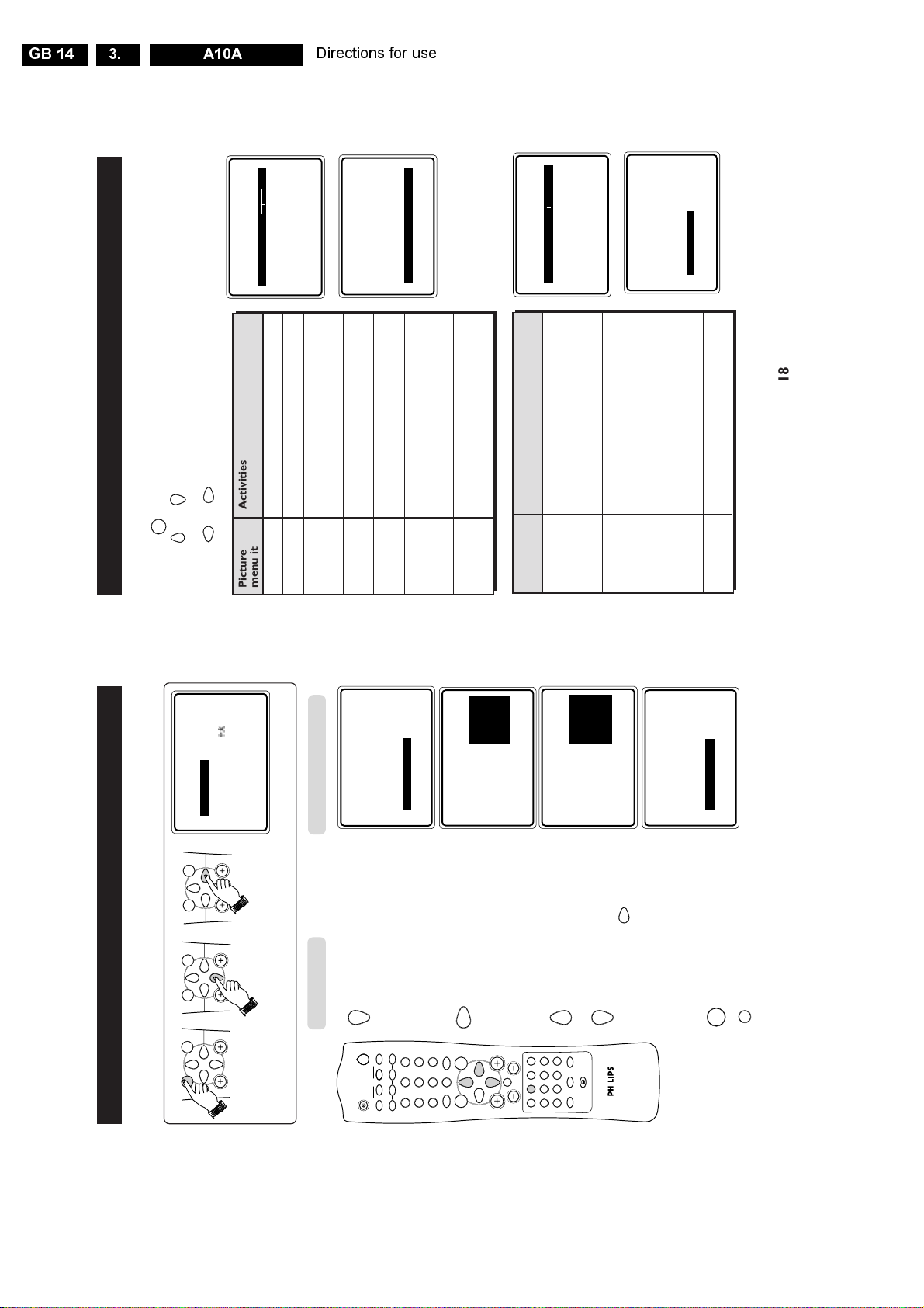
Picture Activities
menu items
Brightness Increase or decrease brightness level.
Colour Increase or decrease color level.
Contrast Increase or decrease contrast level
until lightest parts of the picture show
good detail.
Sharpness Increase or decrease sharpness level
to improve detail in the picture.
Colour Temp Allows you a choice of 3 picture settings
(NORMAL, WARM and COOL).
NR (Noise Allows you to reduce the “noise”
Reduction) (little dots on the picture) from weak
signal broadcast. Selecting the “ON”
option will make the picture clearer.
Incredible Selecting the “ON” option enhances
Picture the details in the picture. The result is
a more dynamic and vivid picture.
U
SING THE
P
ICTURE
/S
OUND
M
ENU
The picture and sound menus allow you to make adjustments to the picture and sound. It also
allow you to select and activate other features in the menu.
1 Press the (MENU) button to enter main menu.
2 Use the or (CURSOR UP/DOWN) buttons to select the items on the
PICTURE/SOUND menu.
3 Use the or (CURSOR LEFT/RIGHT) buttons to access the sub-menus.
Sound Activities
menu items
Treble Increase or decrease the high frequency
level.
Bass Increase or decrease the low frequency
level.
Balance Adjusts the balance of the right and left
speakers’ sound output.
AVL As variation in signal conditions can
(Auto Volume result in a sudden change in volume
Leveller) during commercial breaks or channel
switching, selecting the “ON” function
will enable the volume to remain at a
standard volume level.
Headphone Allows you to adjust the volume and
balance of the headphone
➠
➠
SOUND
TREBLE 38
•
BASS
•
BALANCE
•
AVL
•
HEADPHONE
Ñ
É
PICTURE
BRIGHTNESS 38
•
COLOUR
•
CONTRAST
•
SHARPNESS
•
COLOUR TEMP
Ñ
É
▲
▼
PICTURE
•
CONTRAST
•
SHARPNESS
•
COLOUR TEMP 8
•
NR
INCR. PICTURE
•
ON
Ñ
É
▲
▲
MENU
➠
➠
Note : HUE feature is
only applicable to NTSC
programmes. The HUE item
will not appear on the menu
if programme is in PAL mode.
Note : Headphone feature
does not work if PIP
(Picture-in-Picture) mode
is activated.
Directions for use
HEADPHONE
TREBLE VOLUME
BASS BALANCE
BALANCE
AVL
Ñ
SOUND
•
•
•
•
▲
▲
AUTO STORE
MANUAL STORE
•
•
INSTALL
until NAME is highlighted.
4. Press button repeatedly
r
2
PIP CH
o
PIP
n
A/CH
8
É
•
CHANNEL EDIT
SORT
NAME
Ñ
•
•
UP DN
2
13
vp
ENGLISH
É
▲
INSTALL
HANNELS
C
AMING OF
N
This feature allows a selection of 40 channels for preset names. It also allows you to enter a
SURF
MENU
SURF
MENU
SURF
MENU
new name or modify an existing name of a channel including external channels.
•
LANGUAGE
AUTO STORE B.MELAYU
MANUAL STORE
SORT
CHANNEL EDIT
Ñ
•
•
•
•
➠
➠
➠
▼
Result on TV Screen
Press button
1. Enter main menu. 2. Select INSTALL. 3. Enter install mode.
LUCKY
É
▲
▲
•
CHANNEL EDIT
NAME
AUTO STORE
MANUAL STORE
SORT
Ñ
•
•
•
•
INSTALL
(You can enter up to a
maximum of 5 characters)
7. Store named channel.
MENU
17
8. Exit menu from screen.
m
▲
▲
AUTO STORE
MANUAL STORE
•
•
CHANNEL EDIT
SORT
•
•
LUCKY
É
•
NAME
Ñ
–
É
▲
▲
•
CHANNEL EDIT
AUTO STORE
MANUAL STORE
SORT
NAME
INSTALL
Ñ
•
•
•
•
INSTALL
5. Enter NAME mode
6
9
`
SMARTSMART
5
8
0
±
MENU
7
4
CH
SURF
H
INDEX
A
to cycyle through the
characters and select
desired character.
Move to next character
slot by the (CURSOR
RIGHT) button and select
in the next character.
6. Press button repeatedly
OR
\
`
4m
OK
e
AV
bhfy
INCR. SURR. INCREDIBLE
Page 15
Directions for use
20
A
CTIVATING THE
T
IMER
(C
ONTINUE
)
11. Exit from STOP TIME
mode.
12. Select CHANNEL.
13. Enter the CHANNEL
mode.
14. Key in the channel you
want to switch to.
15. Exit from CHANNEL
mode.
16. Select ACTIVATE.
17. Activate timer. You can
select to activate timer
by DAILY or ONCE
mode.
18. Select DISPLAY.
19. Select ON mode if you
want to display the
current time on the TV
screen.
20. Exit menu from screen.
Note
30 seconds before the timer is activated, a message indicating the time left for the channel
switch will appear on the screen. To disable the channel switch, press any button on the
remote control.
Press button
Result on TV Screen
5
13
2
4
6
7
9
8
0
m
e
A/CH
4m
MENU
SURF
SMARTSMART
±
`
n
o
r
vp
A
CH
H
\
5
13
2
4
6
7
9
8
0
INDEX
AV
INCR. SURR. INCREDIBLE
OK
bhfy
2
PIP
`
PIP CH
UP DN
▲
▼
FEATURES
TIMER
•
TIME
•
START TIME
•
STOP TIME
CHANNEL
•
3
•
ACTIVATE
Ñ
É
▲
▼
FEATURES
TIMER
•
TIME
•
START TIME
•
STOP TIME
CHANNEL
•
8
•
ACTIVATE
Ñ
É
▲
▼
FEATURES
TIMER
•
TIME
•
START TIME
•
STOP TIME
•
CHANNEL
ACTIVATE
•
OFF
Ñ
É
▲
▼
FEATURES
TIMER
•
TIME
•
START TIME
•
STOP TIME
•
CHANNEL
ACTIVATE
•
ONCE
Ñ
É
▲
▼
FEATURES
TIMER
•
START TIME
•
STOP TIME
•
CHANNEL
•
ACTIVATE
DISPLAY
•
ON
Ñ
É
GB 15A10A 3.
▲
TIMER
FEATURES
Result on TV Screen
IMER
T
CTIVATING THE
A
Press button
The Timer feature allows you to set the timer to switch to another channel at a specified
time while you are watching another channel or when the TV is on standby mode.
Note : For the timer to function, the set must not be switched off. Once the set is switched
off, the timer is disabled.
1. Enter TIMER menu.
\
2
PIP
– – : – –
É
▼
•
STOP TIME
START TIME
CHANNEL
TIME
ACTIVATE
Ñ
•
•
•
•
2. Enter TIME mode.
r
6
PIP CH
o
n
A/CH
9
UP DN
2
5
8
7
4
13
vp
▼
▲
12 : 30
É
•
START TIME
TIME
Ñ
TIMER
FEATURES
•
For example, if the current
3. Key in the current time
6
9
2
5
8
7
4
13
`
SURF
SMARTSMART
0
±
MENU
– – : – –
É
▲
•
START TIME
STOP TIME
CHANNEL
ACTIVATE
•
•
•
TIME
•
TIMER
FEATURES
Ñ
time is 12:30, key digit 1
and 2 in the hour column,
followed by digit 3 and 0
in the minute column.
4. Exit from TIME mode.
0
CH
\
4m
H
INDEX
AV
bhfy
A
INCR. SURR. INCREDIBLE
STOP TIME
CHANNEL
ACTIVATE
•
•
•
5. Select START TIME.
`
OK
e
▼
FEATURES
13:30
É
▲
•
START TIME
CHANNEL
STOP TIME
TIME
ACTIVATE
Ñ
•
•
•
TIMER
•
mode.
the programme to be
6. Enter the START TIME
7. Key in the time you want
6
9
2
5
8
7
4
13
▲
▼
FEATURES
switched on.
8. Exit from START TIME
0
START TIME
TIME
•
•
TIMER
mode.
– – : – –
É
•
STOP TIME
CHANNEL
Ñ
•
▼
ACTIVATE
•
9. Select STOP TIME.
TIME
•
TIMER
FEATURES
10. Enter STOP TIME mode.
▲
▼
15: 30
É
•
STOP TIME
START TIME
CHANNEL
ACTIVATE
Ñ
•
•
•
the programme to be
switched off.
11. Key in the time you want
6
9
2
5
8
0
7
4
13
19
Page 16
GB 16 A10A3.
22
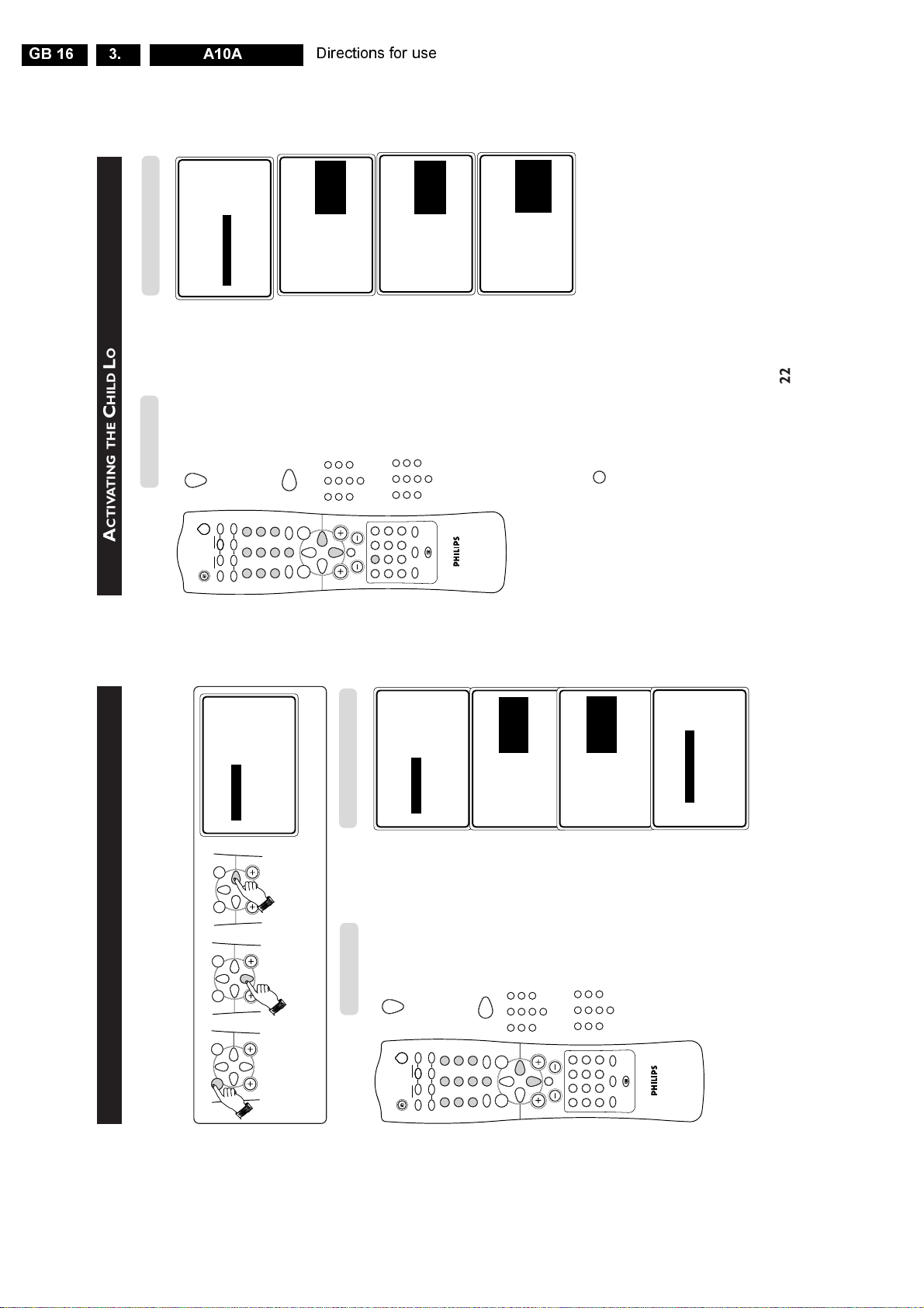
A
CTIVATING THE
C
HILD
L
OCK
(C
HANGE CODE
)
8. Select CHANGE CODE.
9. Enter CHANGE CODE
mode.
10. Key in the access code of
your choice.
11. Confirm access code.
When the new code
is confirmed, the
message CORRECT
will appear.
12. Exit menu from screen.
Note : After you have exit menu from screen and you want to enter child lock menu again ,
you need to key the new access code only once. If you have forgotten the new access code,
key in 0711 twice to enter the child lock menu. Upon entering the child lock menu, you can
proceed to change code again.
Ñ
FEATURES
CHILD LOCK
•
LOCK CHANNEL ENTER
CHANGE CODE NEW CODE
•
CLEAR ALL
X X X X
Ñ
FEATURES
CHILD LOCK
•
LOCK CHANNEL CONFIRM
CHANGE CODE CODE
•
CLEAR ALL
X X X X
Ñ
FEATURES
CHILD LOCK
•
LOCK CHANNEL CONFIRM
CHANGE CODE CODE
•
CLEAR ALL
X X X X
CORRECT
Press button
Result on TV Screen
5
13
2
4
6
7
9
8
0
5
13
2
4
6
7
9
8
0
e
A/CH
4m
MENU
SURF
SMARTSMART
±
`
n
o
r
vp
A
CH
H
\
5
13
2
4
6
7
9
8
0
INDEX
AV
INCR. SURR. INCREDIBLE
OK
bhfy
2
PIP
`
PIP CH
UP DN
m
Ñ
FEATURES
CHILD LOCK
•
LOCK CHANNEL ENTER
CHANGE CODE NEW CODE
•
CLEAR ALL
– – – –
Directions for use
)
ODE
C
CCESS
(A
OCK
L
HILD
C
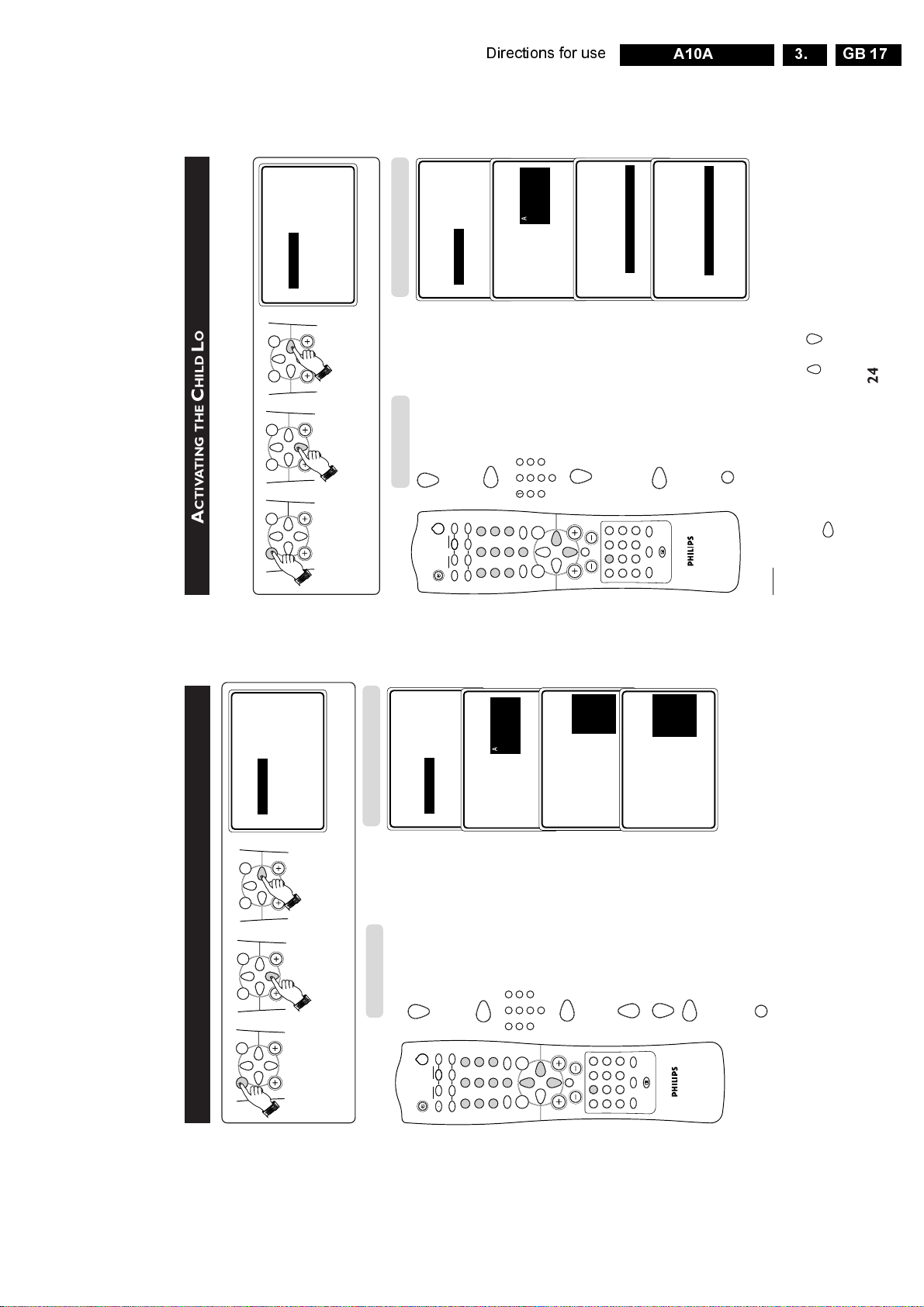
CTIVATING THE
A
The Child Lock feature allows you to lock channels to prevent their children from watching
programmes they deem undesirable.
Note : You cannot have access to the locked channels via the top controls of the TV set.
You can only have access to the locked channels via the remote control.
TIMER TIME
PIP STOP TIME
FORMAT CHANNEL
CHILD LOCK START TIME
BLUE MUTE ACTIVATE
É
▼
▲
•
•
FEATURES
•
•
•
➠
SURF
MENU
➠
SURF
MENU
➠
SURF
MENU
– – – –
TIMER ACCESS CODE
PIP
CHILD LOCK
É
▼
▲
•
FEATURES
•
•
FORMAT
BLUE MUTE
•
•
5. Enter ACCESS CODE
Result on TV Screen
4. Select CHILD LOCK .
Press button
r
2
PIP
1. Enter main menu. 2. Select FEATURES . 3. Enter FEATURES menu.
PIP CH
UP DN
o
2
n
13
vp
A/CH
6
9
`
SMARTSMART
5
8
0
±
7
4
X X X X X
FORMAT
BLUE MUTE
PIP INCORRECT
CHILD LOCK
TIMER ACCESS CODE
É
Ñ
•
•
•
FEATURES
•
FEATURES
mode.
(0711 is the default access
code). A message
INCORRECT will appear.
0
CH
H
A
7. Key in 0711 the second
2
13
\
4m
INDEX
AV
6. Key in access code 0711
6
9
2
5
8
7
4
13
SURF
MENU
▲
X X X X
BLUE MUTE
PI P CORRECT
CHILD LOCK
FORMAT
TIMER ACCESS CODE
É
Ñ
•
•
•
•
FEATURES
time. When the message
CORRECT appears, the
CHILD LOCK menu is
now accessible.
You can now proceed to
6
9
5
8
0
7
4
`
OK
e
bhfy
INCR. SURR. INCREDIBLE
change the access code
2
É
•
LOCK CHANNEL
CHANGE CODE 3
CLEAR ALL 4
Ñ
•
5
6
CHILD LOCK
•
of your choice.
21
Page 17
24
A
CTIVATING THE
C
HILD
L
OCK
(C
LEAR
A
LL
)
To unlock channels that you have locked, enter the Child Lock menu and activate the
CLEAR ALL mode.
1. Enter main menu. 2. Select FEATURES 3. Enter FEATURES menu.
4. Select CHILD LOCK.
5. Enter ACCESS CODE
mode.
6. Key in access code.
7. Press button repeatedly
until CLEAR ALL is
selected.
8. Activate clearing of all
locked channels.
9. Exit menu from screen.
Note
You can also unlock individual channel by the LOCK CHANNEL menu.
• Repeat step 1 to 7 as in “ACTIVATING THE CHILD LOCK (LOCK CHANNEL)”.
• Select the channel you want to unlock by the or (CURSOR UP / DOWN) buttons.
• Press the (CURSOR RIGHT) button to unlock channel (the keylock symbol will
disappear).
Press button
Result on TV Screen
▲
▼
FEATURES
•
TIMER TIME
•
CHILD LOCK START TIME
•
PIP STOP TIME
•
FORMAT CHANNEL
•
BLUE MUTE ACTIVATE
É
▲
▼
FEATURES
•
TIMER ACCESS CODE
•
CHILD LOCK
– – – –
•
PIP
•
FORMAT
•
BLUE MUTE
É
Ñ
FEATURES
•
TIMER ACCESS CODE
CHILD LOCK
X X X X
•
PIP CORRECT
•
FORMAT
•
BLUE MUTE
É
Ñ
FEATURES
CHILD LOCK
•
LOCK CHANNEL
•
CHANGE CODE
CLEAR ALL
•
▲
É
Ñ
FEATURES
CHILD LOCK
•
LOCK CHANNEL
•
CHANGE CODE
CLEAR ALL
•
CLEARED
▲
É
MENU
SURF
MENU
SURF
MENU
SURF
➠
➠
➠
5
13
2
4
6
7
9
8
0
m
e
A/CH
4m
MENU
SURF
SMARTSMART
±
`
n
o
r
vp
A
CH
H
\
5
13
2
4
6
7
9
8
0
INDEX
AV
INCR. SURR. INCREDIBLE
OK
bhfy
2
PIP
`
PIP CH
UP DN
Directions for use
GB 17A10A 3.
)
HANNEL
C
OCK
(L
OCK
L
HILD
C
CTIVATING THE
A
FEATURES
➠
SURF
MENU
➠
SURF
MENU
SURF
MENU
TIMER TIME
BLUE MUTE ACTIVATE
PIP STOP TIME
FORMAT CHANNEL
CHILD LOCK START TIME
É
▼
▲
•
•
•
•
•
➠
Result on TV Screen
Press button
1. Enter main menu. 2. Select FEATURES. 3. Enter FEATURES menu.
4. Select CHILD LOCK .
– – – –
TIMER ACCESS CODE
PIP
CHILD LOCK
É
▼
▲
•
FEATURES
•
•
r
2
o
PIP
n
A/CH
FORMAT
BLUE MUTE
•
•
FEATURES
5. Enter ACCESS CODE
6
PIP CH
UP DN
2
5
4
13
vp
▲
X X X X
TIMER ACCESS CODE
CHILD LOCK
PIP CORRECT
FORMAT
BLUE MUTE
É
Ñ
•
•
•
•
FEATURES
mode.
6. Key in access code .
6
9
2
5
8
0
7
4
13
9
`
SURF
SMARTSMART
8
0
±
MENU
7
2
É
•
LOCK CHANNEL
CHANGE CODE 3
Ñ
CHILD LOCK
•
CLEAR ALL 4
•
▲
5
6
FEATURES
CHILD LOCK
mode.
7. Enter LOCK CHANNEL
8. Select the channel you
OR
CH
\
`
4m
H
INDEX
AV
A
bhfy
INCR. SURR. INCREDIBLE
OK
e
3 F
É
•
LOCK CHANNEL
CHANGE CODE 4
CLEAR ALL 5
Ñ
•
6
7
•
want to block.
9. Activate blocking of
channel. A keylock symbol
will appear beside the
channel number indicating
that it is locked.
10. Exit menu from screen.
m
Note : You cannot have access to the locked channels via the top controls of the TV set.
You can only have access to the locked channels via the remote control.
to enable you to enter the INSTALL menu.
If you attempt to enter the INSTALL menu after locking a channel, a message
“Enter ACCESS CODE” will appear on the screen. You need to enter the ACCESS CODE
23
Page 18
GB 18 A10A3.
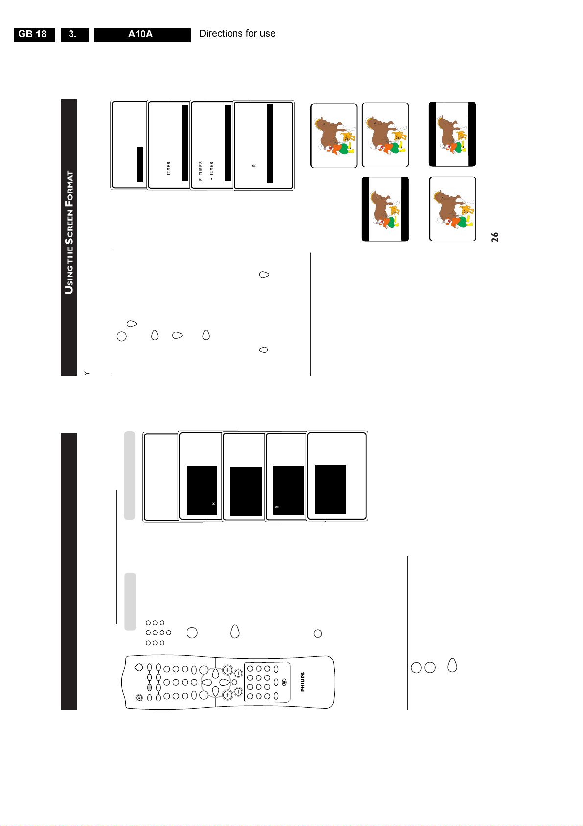
26
U
SING THE
S
CREEN
F
ORMAT
You can have a choice of different formats for your viewing pleasure, namely : - 4:3 mode,
EXPAND 4:3 mode and COMPRESS 16:9 mode through the FORMAT menu.
How to access the Screen Format
1. Press the (MENU) button to enter main menu
and press the (CURSOR DOWN) button
repeatedly until FEATURES is selected.
2. Press the (CURSOR RIGHT) button to
enter FEATURES menu.
3. Press the (CURSOR DOWN) button
repeatedly until FORMAT is selected.
4. Press the (CURSOR RIGHT) button
repeatedly to cycle through the different formats
(4:3, Expand 4:3 or Compress 16:9) and select
your desired format.
Note : You can also select your desired Screen Format
by the (CURSOR UP) and (CURSOR DOWN)
buttons.
When to use the Screen Formats
4:3 format
Select the 4:3 format if you want to display
the 4:3 picture using the full surface of the
screen.
Expand 4:3 format
Select the Expand 4:3 format if you want
to expand movie images recorded in the
letterbox format. When this format is
selected, the black horizontal bars at the
top and bottom are expanded thus filling
up the entire TV screen.
Compress 16:9 format
Select the Compress 16:9 format if you
want to compress full screen movie images
into letterbox format. When this format is
selected, black horizontal bars can be seen
at the top and bottom of the TV screen.
➠
➩
➩
➠
➩
➩
•
PICTURE
TIMER
•
SOUND
CHILD LOCK
•
FEATURES
PIP
•
INSTALL
FORMAT
BLUE MUTE
É
▼
▲
▲
FEATURES
•
TIMER
•
CHILD LOCK
•
PIP
FORMAT
•
4:3
•
BLUE MUTE
Ñ
É
▼
▲
FEATURES
•
TIMER
•
CHILD LOCK
•
PIP
FORMAT
•
EXPAND 4:3
•
BLUE MUTE
Ñ
É
▼
MENU
▲
FEATURES
•
TIMER
•
CHILD LOCK
•
PIP
FORMAT
•
COMPRESS 16:9
•
BLUE MUTE
Ñ
É
▼
Directions for use
ONTROL
C
URF
S
SING THE
U
A list or series of previously viewed channels can be selected with the SURF button. This
feature allows you to switch between different TV programmes that currently interest you.
You can set up to a maximum of eight channels in the SURF list.
8
Result on TV Screen
1. Select a channel you
Press button
2
13
r
2
PIP CH
o
PIP
n
A/CH
want to add to the
surf list.
6
9
5
8
0
7
4
6
9
UP DN
2
5
8
7
4
13
vp
How to add a channel to the surf list
8 ADD?
É
SURF
•
2. Enter SURF menu.
SURF
`
SURF
SMARTSMART
0
±
MENU
8 DELETE?
Ñ
É
SURF LIST EMPTY
SURF
•
the surf list.
3, Add selected channel to
CH
H
INDEX
A
Ñ
SURF
8 • 5 ADD?
É
•
8 • 5 DELETE?
É
Ñ
SURF
•
Ñ
25
Repeat steps 1 - 3 to add
more channels to the
surf list.
\
`
4m
AV
bhfy
INCR. SURR. INCREDIBLE
OK
e
addind the selected
channels to the surf list,
exit menu from screen.
4. After you have completed
m
Note : To view the the selected channels in the surf list, press the SURF button repeatedly
SURF
SURF
to cycle through the channels.
How to delete a channel from the surf list
1. Press the (SURF) button to display surf list.
2. Press the (SURF) button repeatedly to cycle through the surf list and select the
channel you want to delete.
3. Press the (CURSOR RIGHT) button to delete channel from the surf list.
4. Repeat all the above steps if you want to delete more channels from the surf list.
Page 19
Directions for use
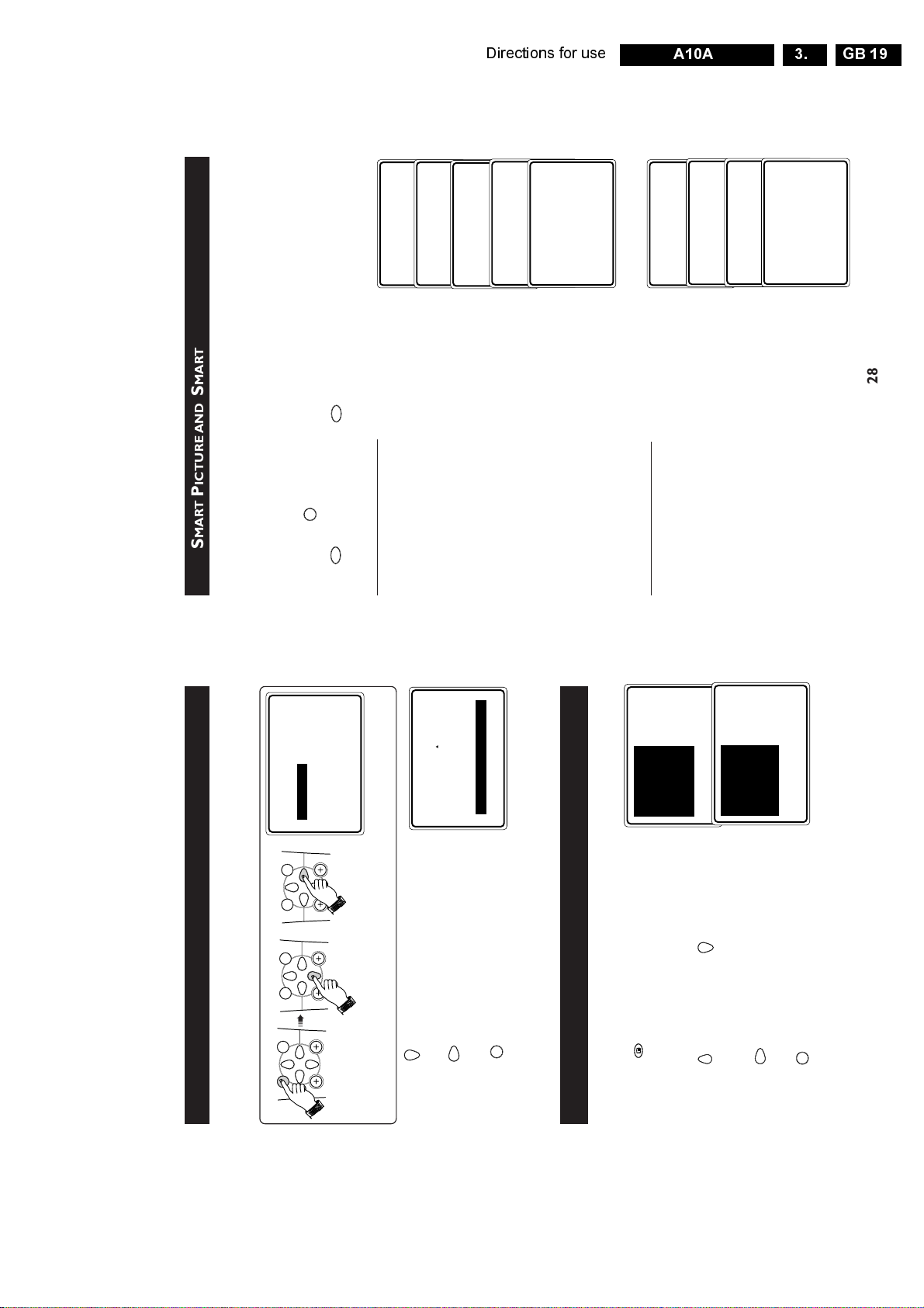
28
S
MART
P
ICTURE AND
S
MART
S
OUND
C
ONTROL
SMART PICTURE feature offers you a choice of 5 picture settings, namely, RICH,
NATURAL, SOFT, PERSONAL and MULTIMEDIA.
SMART SOUND feature offers you a choice of 4 sound settings, namely, THEATRE,
MUSIC, VOIC E and PERSONAL.
Note : If you want to view the pre-set settings for Brightness, Colour, Contrast and Sharpness
levels, for Smart Picture and pre-set settings for Treble and Bass levels for Smart Sound, you
must press the (OSD) button for 5 seconds.
Press (SMART PICTURE) or (SMART SOUND) button repeatedly to cycle
through the settings to select your desired mode.
Definition of Picture Settings
PERSONAL : Picture settings are set to your preference.
RICH : Emphasize very vibrant colours.
(Suitable for AV mode in brightly-lit room)
NATURAL : Emphasize original colours.
SOFT : Emphasize “warm” colours.
(Suitable for dimly-lit room condition and
gives cinema-like effect when light is
switched off).
MULTIMEDIA : Emphasize “soft” colours. (Suitable for
playing computer games, surfing, etc.)
Note : The PERSONAL setting is the setting that you
set up using the Picture menu in the main menu. This
is the only setting in the Smart Picture settings that
can be changed. All the other settings are pre-set at
the factory.
Definition of Sound Settings
PERSONAL : Sound settings are set to your preference.
VOICE : Emphasize high tone. (Treble boosted)
MUSIC : Emphasize low tone. (Bass boosted)
THEATRE : Emphasize sensation to action.
(Bass and Treble boosted)
SMART
`
m
SMART
±
PERSONAL
RICH
NATURAL
SOFT
MULTIMEDIA
PERSONAL
VOICE
NATURAL
SOFT
GB 19A10A 3.
TIMER TIME
PIP STOP TIME
FORMAT CHANNEL
CHILD LOCK START TIME
BLUE MUTE ACTIVATE
É
▼
▲
•
•
FEATURES
•
•
•
ONTROL
C
UTE
SURF
➠
M
MENU
LUE
B
CTIVATING THE
A
The Blue Mute feature indicates to you the absence of signal in the transmission when the
SURF
MENU
“ON” option is activated. Upon the detection of absence of signal, the TV screen will turn
blue in colour.
➠
SURF
MENU
➠
1. Enter main menu. 2. Select FEATURES. 3. Enter the FEATURES menu.
FEATURES
until BLUE MUTE is selected.
4. Press the (CURSOR DOWN) button repeatedly
▲
TIMER
CHILD LOCK
•
•
OFF
É
•
PIP
FORMAT
Ñ
BLUE MUTE
•
•
to activate blue mute feature.
5. Press the (CURSOR RIGHT) button to select ON
m
6. Press the (OSD) button to exit menu from screen.
EATURE
F
ISTING
L
ROGRAMME
P
SING THE
U
Programme listing feature allows you to navigate through a list of installed programmes for a
▲
PROGRAM LIST
OK
quick overview of the channels and activate the channel you have selected.
1. Press the (PROGRAMME LIST) button to
_ _ _ _ _
_ _ _ _ _
_ _ _ _ _
_ _ _ _ _
_ _ _ _ _
2
1
5
4
Ñ
É
▼
•
3
display the list of installed programmes. The current
channel is highlighted.
2. Press the (CURSOR UP) or (CURSOR DOWN)
F
_ _ _ _ _
DRAMA
ACTIO
2
1
5
4 ROMAN
Ñ
É
▼
▲
PROGRAM LIST
3 VIOLE
•
button to cycle through the programme list and
highlight the channel number you want to activate.
the channel you have selected.
3. Press the (CURSOR RIGHT) button to activate
27
m
4. Press the (OSD) button to exit menu from screen.
Page 20
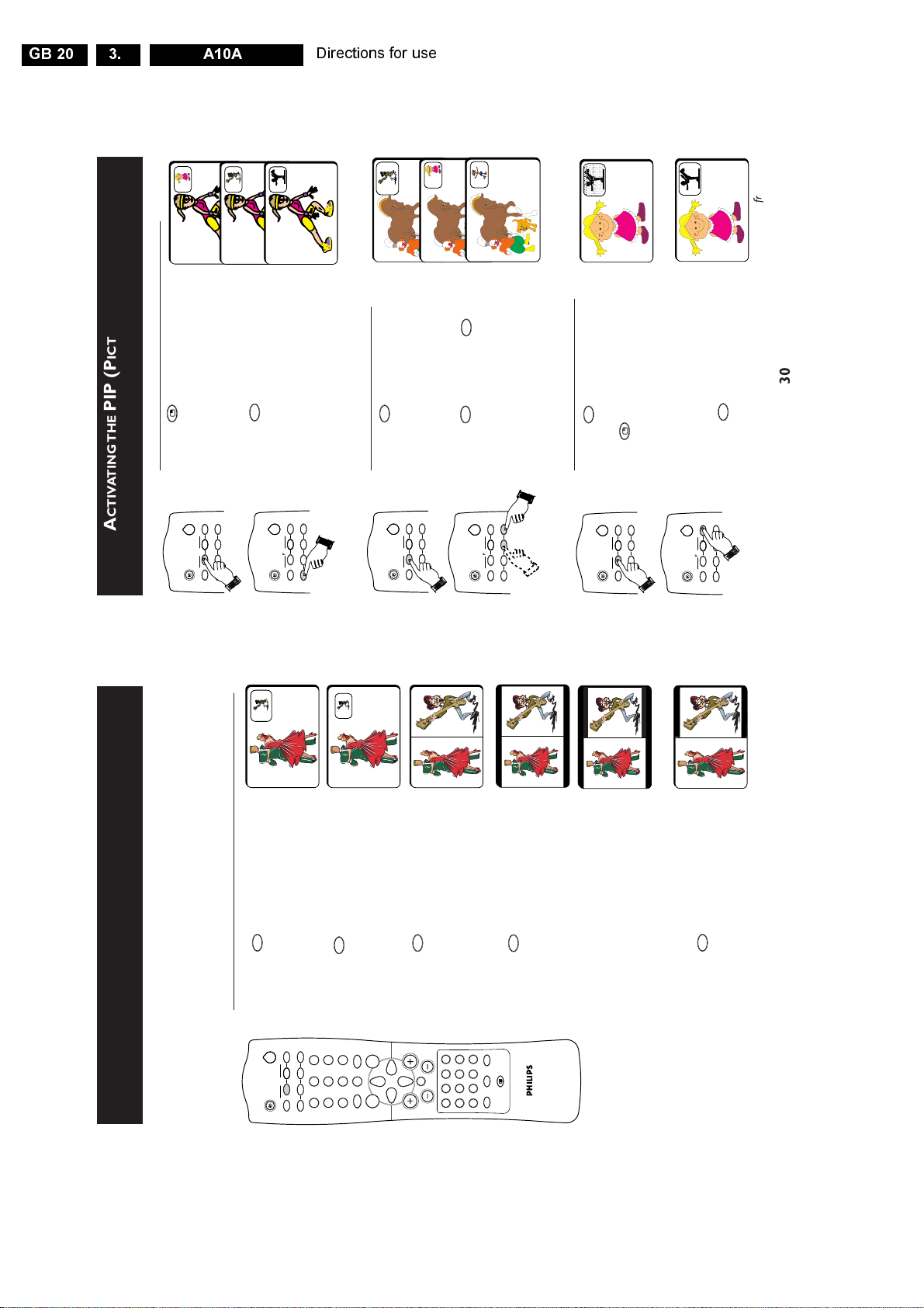
GB 20 A10A3.
30
A
CTIVATING THE
PIP (P
ICTURE-IN-
P
ICTURE
)
C
ONTROL
How to select the various external sources
• Press the (PIP On/Off) button
to switch on PIP screen.
• Press the (PIP Source) button
repeatly to cycle through the various
external connections and select the
desired PIP source.
How to select a PIP channel
• Press the (PIP On/Off) button to
switch on PIP screen.
• Press the (PIP Up) or (PIP
Down) button to select a PIP channel
in ascending or descending order.
How to freeze the PIP screen
• Press the (PIP On/Off) button
to switch on PIP screen.
• Press (PIP Freeze) button once
to freeze the PIP screen
.
Freezing the PIP
screen allows you to view a programme
in the still mode. For example, you may
want to write down some information
from the PIP screen, freezing the screen
will allow you time to do so.
• Press the (PIP Freeze) button
the second time to unfreeze the
PIP screen.
2
3
4
AV1
AV2
AV2
A/CH
n
o
r
vp
2
PIP
PIP CH
UP DN
A/CH
n
o
r
vp
2
PIP
PIP CH
UP DN
A/CH
n
o
r
vp
2
PIP
PIP CH
UP DN
A/CH
n
o
r
vp
2
PIP
PIP CH
UP DN
A/CH
n
o
r
vp
2
PIP
PIP CH
UP DN
A/CH
n
o
r
vp
2
PIP
PIP CH
UP DN
PIP Freeze
PIP Unfreeze
n
r
r
n
DN
UP
n
v
Directions for use
)
ICTURE
P
ICTURE-IN-
PIP (P
CTIVATING THE
A
ONTROL
C
INDOW
W
OUBLE
D
AND
Picture-in-Picture feature allows you to call up a subscreen within your main screen
n
How to switch on the PIP/Double Window screen
• Press the (PIP On/Off) button
2
enabling you to watch two channels at the same time.
Double Window feature allows you to divide the main screen into two sub-screens
enabling two channels to be watched simultaneously.
Note : PIP and Double Window features cannot be activated when teletext mode is on.
to switch on PIP mode. (A normal size
PIP screen appears).
r
6
PIP CH
UP DN
o
2
PIP
5
n
4
13
vp
A/CH
n
time to change the normal size PIP
screen to a smaller size.
• Press the button the second
9
`
SMARTSMART
8
0
±
7
n
to switch to Double Window screens
in 4:3 format.
• Press the button the third time
CH
SURF
MENU
\
4m
H
INDEX
AV
A
bhfy
INCR. SURR. INCREDIBLE
to switch off 16:9 Double Window
screens.
4:3 format (NTSC mode)
29
16:9 format (NTSC mode)
smaller.
n
• Press the button the fifth time
n
to switch to Double Window screens
in 16:9 format.
Note : When the programme on the
PIP screen is in NTSC mode or
transmission, the picture size appears
smaller. Likewise, when programme on
the main screen is in NTSC mode or
transmission, the picture size appears
• Press the button the fourth time
`
OK
e
Page 21
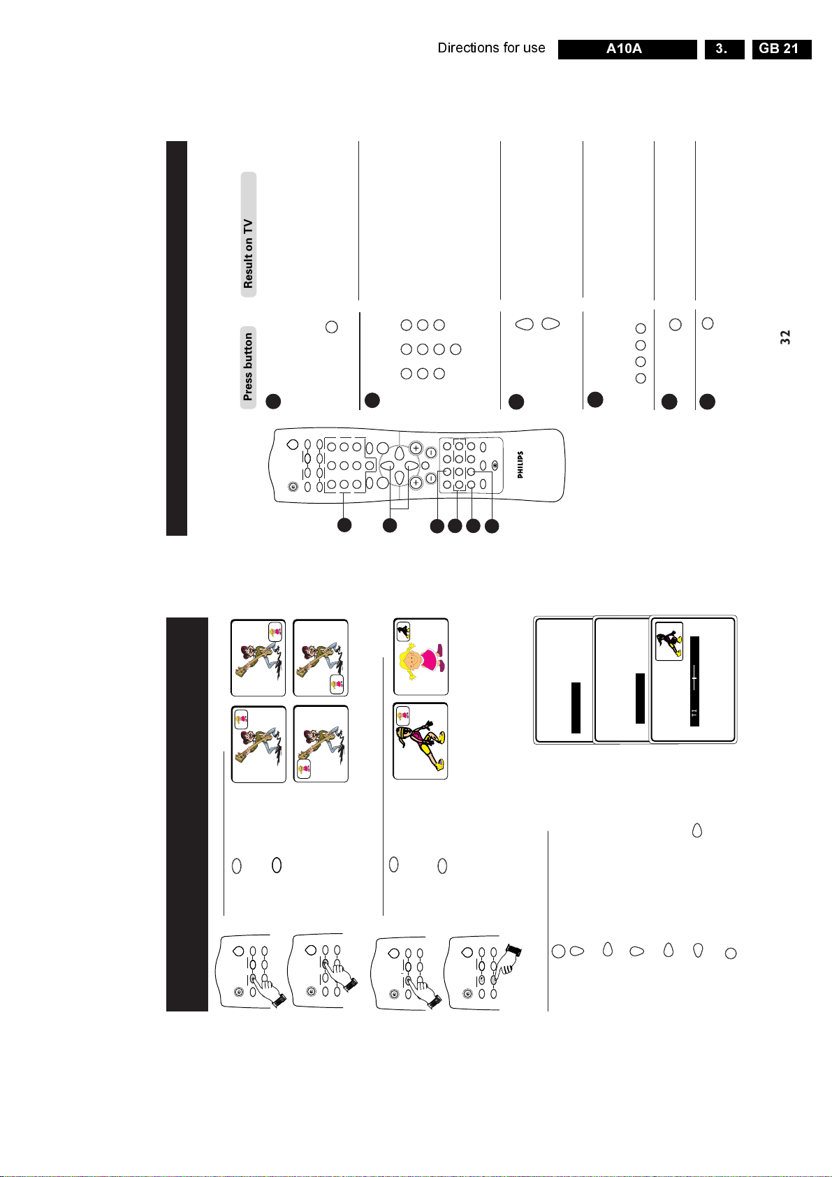
Directions for use
32
Press button
Result on TV Screen
e
A/CH
4m
MENU
SURF
SMARTSMART
±
`
n
o
r
vp
A
CH
H
\
5
13
2
4
6
7
9
8
0
INDEX
AV
INCR. SURR. INCREDIBLE
OK
bhfy
2
PIP
`
PIP CH
UP DN
2
3
4
1
5
6
m
INDEX
h
5
13
2
4
6
7
9
8
0
b
U
SING THE
T
ELEXTEXT
If a TV channel broadcast contains teletext information, each channel that broadcasts
teletexttransmits a page (index page) with information on how to use the teletext system,
usually on page 100. The system transmitted is indicated in the option line at the bottom
of the screen.
1 On/Off teletext Press the button once to switch on
and teletext display. (A channel in which
Superimpose teletext is being transmitted must be
teletext page selected).
over TV Press the button the second time
programme superimpose the teletext page over
the TV programme.
Press the button the third time
to exit teletext mode.
2 Selecting a Key in the required teletext page
teletext page (3 digits). The page number is
displayed at the top left hand corner
of the screen. When the teletext
page is located, the counter stops
searching. If the counter keeps
searching, it means that the page is
not available for selection. If you
make a mistake in keying the page
number, you have to complete
keying the 3-digit number before
re-keying the correct page number.
3 Accessing Press the CURSOR UP button to
a teletext display the next page and the
page CURSOR DOWN button to display
the previous page.
4 Direct Access to The 4-colour buttons allow you to
an item or access directly an item or
corresponding corresponding pages.
pages
5 Main Index Press the button to return to the
main index page.
6 Enlarge Press the button once to enlarge and
view the top half of the page. Press
the button the second time to enlarge
and view the bottom half of the page.
Press the button the third time to
return to normal size page.
GB 21A10A 3.
)
ICTURE
P
ICTURE-IN-
PIP (P
CTIVATING THE
ONTROL
C
A
n
How to position the PIP screen
• Press the (PIP On/Off)
2
PIP
➠
➠
➠
➠
o
button to switch on PIP
screen.
button repeatedly to your
desired position. (You can
• Press the (PIP Position)
r
PIP CH
UP DN
o
n
vp
A/CH
choose the PIP screen to be on
the top left corner, top right
corner, bottom right corner
r
2
PIP CH
UP DN
o
PIP
n
vp
A/CH
➠
➠
n
How to swap the PIP screen and the main screen
or the top bottom left corner).
• Press the (PIP On/Off)
2
PIP
button to switch on PIP
screen.
• Press the (PIP Swap)
r
PIP CH
UP DN
o
n
vp
A/CH
p
button to swap the programme
in the PIP screen and the
2
programme in the main screen.
r
PIP CH
UP DN
o
PIP
n
vp
A/CH
FORMAT
TIMER
BLUE MUTE
CHILD LOCK
PIP
TIMER HUE
BLUE MUT
PIP
FORMAT
CHILD LOCK
É
▼
▲
PICTURE
SOUND
FEATURES
INSTALL
É
▲
▼
•
•
•
•
MENU
How to adjust the PIP Hue setting
repeatedly until FEATURES is selected.
1. Press the (MENU) button to enter main menu.
2. Press the (CURSOR DOWN) button
3. Press the (CURSOR RIGHT) button to enter
•
FEATURES
•
•
the FEATURES menu.
4. Press the (CURSOR DOWN) button repeatedly
•
•
until PIP is selected.
▲
Ñ
FEATURES
PIP
TINT 8
m
PIP menu.
RIGHT) button to adjust HUE setting to your desired level.
5. Press the (CURSOR RIGHT) button to enter
6. Press the (CURSOR LEFT) or (CURSOR
7. Press the (OSD) button to exit menu from screen.
31
Note : Hue adjustments in the PIP programmes will only
take effect if programmes are in NTSC mode.
Page 22
GB 22 A10A3.
34
Suggested Colour / Sound Systems
Destination Colour System Sound System
Singapore PAL B/G
Hong Kong PAL I
Middle East SECAM B/G, D/K
New Zealand PAL B/G
Australia PAL B/G
India PAL B/G
South Africa PAL I
S
PECIFICATIONS
29PT6361 34PT6361
Picture tube screen size 72 cm 85 cm
Picture tube visible area 68 cm 80 cm
Audio Output
Speaker 2 x 10 W
Subwoofer 10 W
Set Dimensions
Width 79 cm 89 cm
Depth 50 cm 56 cm
Height 59 cm 69 cm
Net Weight of Set approximate 45 kg approximate 64 kg
TV System
Colour Sound
PAL B/G
PAL D/ K
PAL I
NTSC (4.43) B/G
NTSC (3.58 ) M
SECAM B/G
SECAM D/K
Note
For Operating Voltage, Frequency, Power Consumption and Version Number, refer to the
type number at the rear of the set.
Directions for use
)
ONTINUE
Result on TV Screen
(C
f
ELETEXT
T
Press button
7 Hold A selected page sometimes contains
SING THE
U
2
PIP
a few sub-pages. The sub-page will
automatically move to the next sub-
page after about 20 seconds. The
total number of sub-pages are
indicated at the top right hand corner
of the screen. Press the button once
r
6
9
PIP CH
UP DN
o
n
vp
A/CH
SMARTSMART
2
5
8
7
4
13
to hold page and the second time to
release holding of page.
teletext page number (the teletext
page must have sub-pages in it).
Press the button and “– – – – “ is
displayed at the upper left hand corner.
Enter the subpage with 4 digits : e.g.
0003 for 3/4 (third of 4 pages). You can
also use the Cursor Left and Right
buttons to access the sub-page. To
cancel the subcode, press button again.
y
Display a sub-page and hold it. Enter the
8 Subcode/Time By adding a sub-code, you can call up
8
9
CH
\
`
SURF
0
±
MENU
H
A
INDEX
`
4m
AV
bhfy
INCR. SURR. INCREDIBLE
OK
e
7
Pressing this button during normal
viewing (only applicable to those
channels that is broadcasting teletext),
the time will be displayed at the top
right hand corner of the screen.
riddles, etc). Press the button the
second time to conceal information.
e
Conceal information (solutions to puzzles,
9 Reveal/ Press the button once to reveal hidden
This button is applicable only to
teletext page with puzzles, riddles, etc.)
6
33
9
2
5
8
0
7
4
13
MENU
b
alphabets at the bottom of the screen is now changed to page numbers.
How to select your favourite page
This feature allows you select 4 of your favourite or most commonly viewed page and stored
them in the favourite page selection. You can then access directly your favourite page by the
colour buttons without having to key in the page number.
1. Press the TELEXTEXT ON/OFF) button to enter teletext mode.
2. Press the (MENU) button to enter favourite page selection. Note : The colour
m
INDEX
3. Key in your favourite page by the (DIGIT 0 -9) buttons.
4. Press the (INDEX/OSD) button to highlight pager numbers.
5. Select the colour button on your remote control you want your favourite page to be stored.
6. Repeat step 3 to 5 to select and store other favourite pages.
Page 23
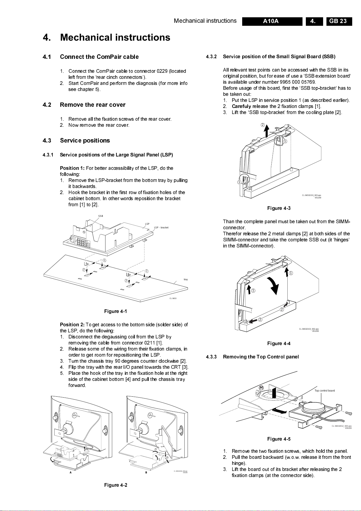
" #
Mechanical instructions
GB 23A10A 4.
4.1 Connect the ComPair cable
1. Connect the ComPair cable to connector 0229 (located
left from the ‘rear cinch connectors’).
2. Start ComPair and perform the diagnosis (for more info
see chapter 5).
4.2 Remove the rear cover
1. Remove all the fixation screws of the rear cover.
2. Now remove the rear cover.
4.3 Service positions
4.3.1 Service positions of the Large Signal Panel (LSP)
Position 1:
following:
1. Remove the LSP-bracket from the bottom tray by pulling
2. Hook the bracket in the first row of fixation holes of the
For better accessibility of the LSP, do the
it backwards.
cabinet bottom. In other words reposition the bracket
from [1] to [2].
SSB
LSP
LSP - bracket
4.3.2 Service position of the Small Signal Board (SSB)
All relevant test points can be accessed with the SSB in its
original position, but for ease of use a 'SSB extension board'
is available under number 9965 000 05769.
Before usage of this board, first the 'SSB top-bracket' has to
be taken out:
1. Put the LSP in service position 1 (as described earlier).
2.
Carefuly
release the 2 fixation clamps [1].
3. Lift the ‘SSB top-bracket’ from the cooling plate [2].
2
1
1
CL 06532153_003.eps
051200
Figure 4-3
Than the complete panel must be taken out from the SIMM-
connector.
Therefor release the 2 metal clamps [2] at both sides of the
SIMM-connector and take the complete SSB out (it 'hinges'
in the SIMM-connector).
1
2
2
1
Bottom tray
CL 06532045_026.eps
270400
Figure 4-1
Position 2:
To get access to the bottom side (solder side) of
the LSP, do the following:
1. Disconnect the degaussing coil from the LSP by
removing the cable from connector 0211 [1].
2. Release some of the wiring from their fixation clamps, in
order to get room for repositioning the LSP.
3. Turn the chassis tray 90 degrees counter clockwise [2].
4. Flip the tray with the rear I/O panel towards the CRT [3].
5. Place the hook of the tray in the fixation hole at the right
side of the cabinet bottom [4] and pull the chassis tray
forward.
1
1
2
3
2
Figure 4-4
4.3.3 Removing the Top Control panel
M
CL 06532153_002.eps
051200
Top control board
CL 06532012_003.eps
030200
1
2
1
2
A
3
4
1. Remove the two fixation screws, which hold the panel.
2. Pull the board backward (w.o.w. release it from the front
hinge).
CL 06532045_028.eps
B
191200
3. Lift the board out of its bracket after releasing the 2
fixation clamps (at the connector side).
Figure 4-2
Figure 4-5
Page 24
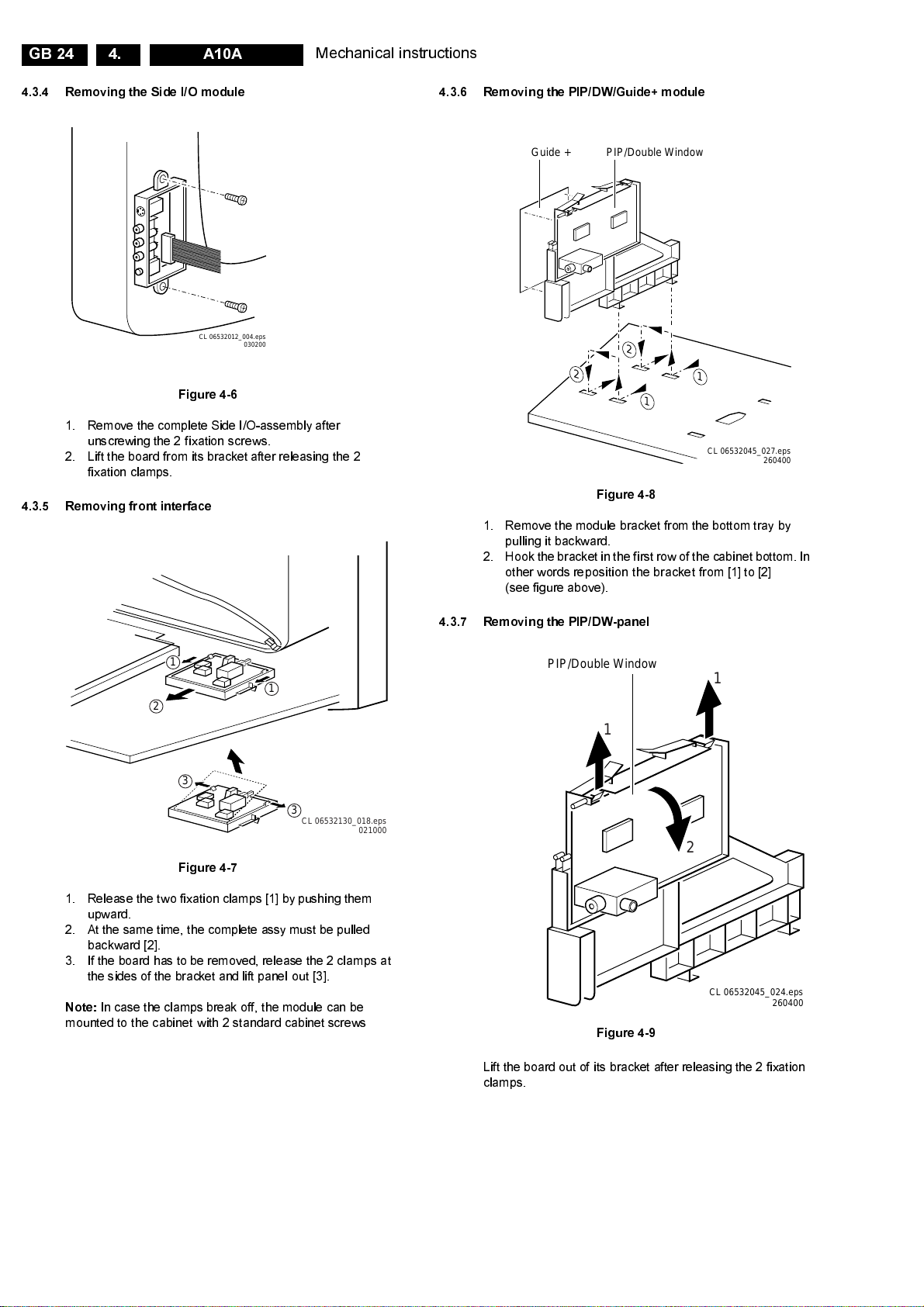
GB 24 A10A4.
2
1
1
2
Mechanical instructions
4.3.4 Removing the Side I/O module
CL 06532012_004.eps
030200
Figure 4-6
1. Remove the complete Side I/O-assembly after
unscrewing the 2 fixation screws.
2. Lift the board from its bracket after releasing the 2
fixation clamps.
4.3.5 Removing front interface
4.3.6 Removing the PIP/DW/Guide+ module
PIP/Double WindowGuide +
CL 06532045_027.eps
Figure 4-8
1. Remove the module bracket from the bottom tray by
pulling it backward.
2. Hook the bracket in the first row of thecabinet bottom. In
other words reposition the bracket from [1] to [2]
(see figure above).
260400
1
1
2
3
3
CL 06532130_018.eps
021000
Figure 4-7
1. Release the two fixation clamps [1] by pushing them
upward.
2. At the same time, the complete assy must be pulled
backward [2].
3. If the board has to be removed, release the 2 clamps at
the sides of the bracket and lift panel out [3].
Note:
In case the clamps break off, the module can be
mounted to the cabinet with 2 standard cabinet screws
4.3.7 Removing the PIP/DW-panel
PIP/Double Window
1
2
Figure 4-9
Lift the board out of its bracket after releasing the 2 fixation
clamps.
1
CL 06532045_024.eps
260400
Page 25
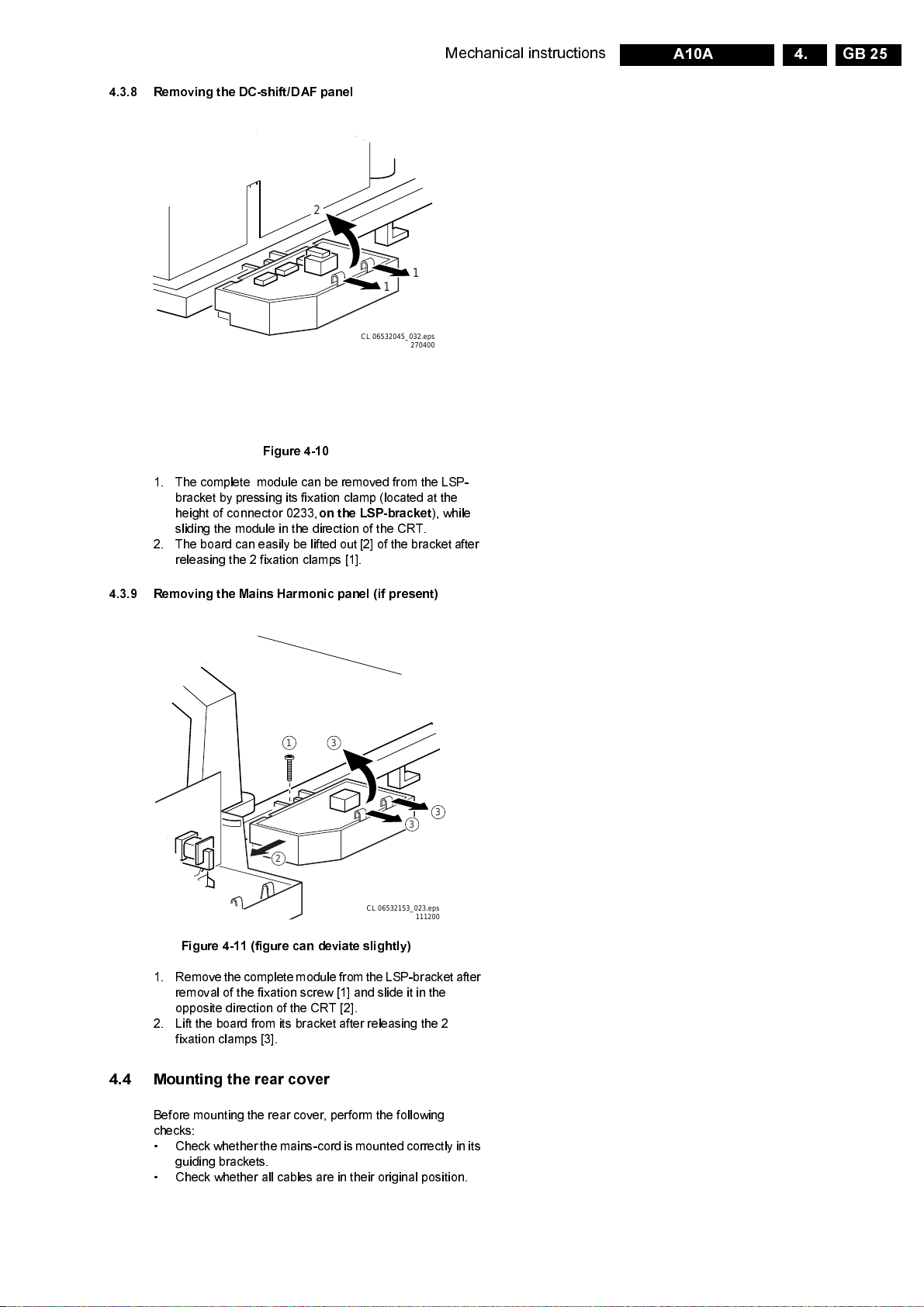
4.3.8 Removing the DC-shift/DAF panel
2
Mechanical instructions
GB 25A10A 4.
1
1
CL 06532045_032.eps
270400
Figure 4-10
1. The complete module can be removed from the LSP-
bracket by pressing its fixation clamp (located at the
height of connector 0233,
on the LSP-bracket
sliding the module in the direction of the CRT.
2. The board can easily be lifted out [2] of the bracket after
releasing the 2 fixation clamps [1].
4.3.9 Removing the Mains Harmonic panel (if present)
31
), while
2
CL 06532153_023.eps
Figure 4-11 (figure can deviate slightly)
1. Remove the completemodulefromthe LSP-bracket after
removal of the fixation screw [1] and slide it in the
opposite direction of the CR T [2].
2. Lift the board from its bracket after releasing the 2
fixation clamps [3].
4.4 Mounting the rear cover
Before mounting the rear cover, perform the following
checks:
• Check whether themains-cord is mountedcorrectly in its
guiding brackets.
• Check whether all cables are in their original position.
3
3
111200
Page 26
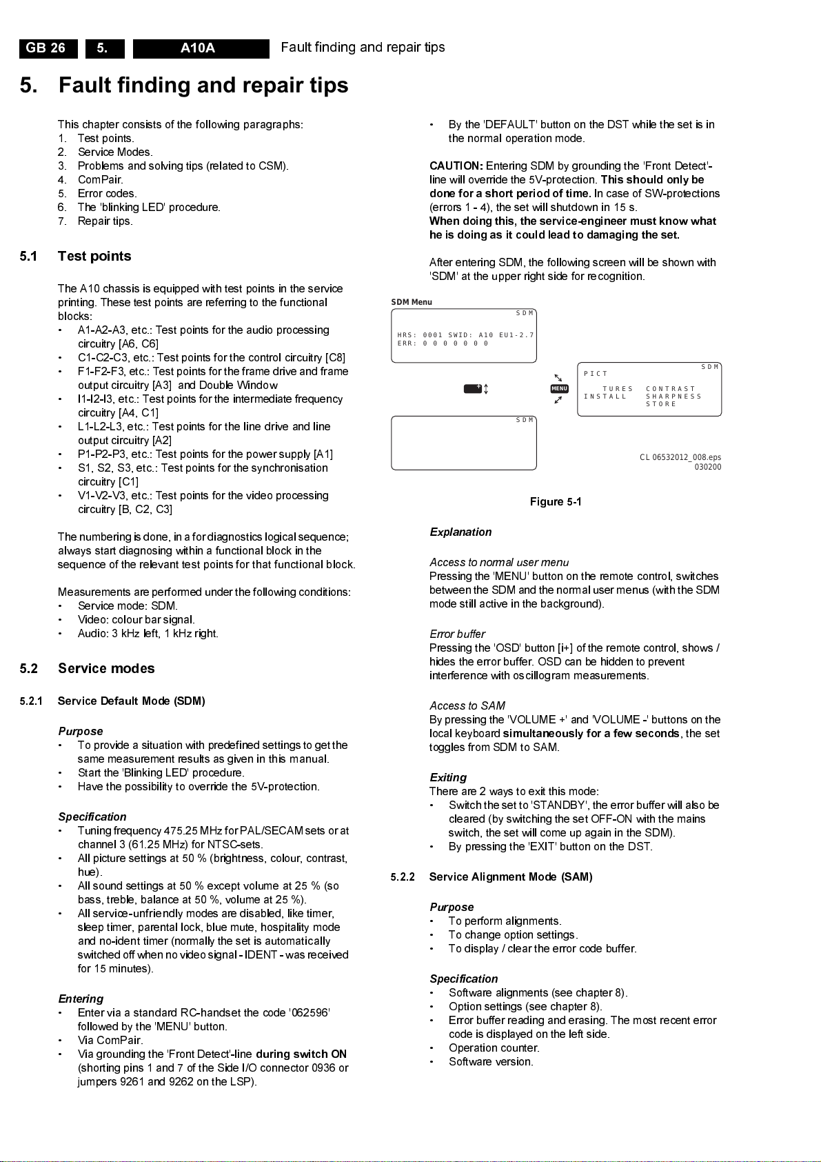
GB 26 A10A5.
Fault finding and repair tips
$ %
This chapter consists of the following paragraphs:
1. Test points.
2. Service Modes.
3. Problems and solving tips (related to CSM).
4. ComPair.
5. Error codes.
6. The 'blinking LED' procedure.
7. Repair tips.
5.1 Test points
The A10 chassis is equipped with test points in the service
printing. These test points are referring to the functional
blocks:
• A1-A2-A3, etc.: Test points for the audio processing
circuitry [A6, C6]
• C1-C2-C3, etc.: Test points for the control circuitry [C8]
• F1-F2-F3, etc.: Test points for theframe drive and frame
output circuitry [A3] and Double Window
• I1-I2-I3, etc.: Test points for the intermediate frequency
circuitry [A4, C1]
• L1-L2-L3, etc.: Test points for the line drive and line
output circuitry [A2]
• P1-P2-P3, etc.: Test points for the power supply [A1]
• S1, S2, S3, etc.: Test points for the synchronisation
circuitry [C1]
• V1-V2-V3, etc.: Test points for the video processing
circuitry [B, C2, C3]
The numbering is done, in a for diagnostics logical sequence;
always start diagnosing within a functional block in the
sequence of the relevant test points for that functional block.
Measurements are performed under the following conditions:
• Service mode: SDM.
• Video: colour bar signal.
• Audio: 3 kHz left, 1 kHz right.
5.2 Service modes
• By the 'DEFAULT' button on the DST while the set is in
the normal operation mode.
CAUTIO N:
line will override the 5V-protection.
done for a short period of time.
Entering SDM by grounding the 'Front Detect'-
This should only be
In case of SW-protections
(errors 1 - 4), the set will shutdown in 15 s.
When doing this, the service-engineer must know what
he is doing as it could lead to damaging the set.
After entering SDM, the following screen will be shown with
'SDM' at the upper right side for recognition.
SDM Menu
HRS: 0001 SWID: A10 EU1-2.7
ERR: 0 0 0 0 0 0 0
SDM
PICTURE BRIGHTNESS
+
SDM
SOUND COLOURNESS
MENU
FEATURES CONTRAST
INSTALL SHARPNESS
Figure 5-1
Explanation
Access to normal user menu
Pressing the 'MENU' button on the remote control, switches
between the SDM and the normal user menus (with theSDM
mode still active in the background).
Error buffer
Pressing the 'OSD' button [i+] of the remote control, shows /
hides the error buffer. OSD can be hidden to prevent
interference with oscillogram measurements.
SDM
STORE
CL 06532012_008.eps
030200
5.2.1 Service Default Mode (SDM)
Purpose
• To provide a situation with predefined settings to get the
same measurement results as given in this manual.
• Start the 'Blinking LED' procedure.
• Have the possibility to override the 5V-protection.
Specification
• Tuning frequency475.25 MHz for PAL/SECAM sets or at
channel 3 (61.25 MHz) for NTSC-sets.
• All picture settings at 50 % (brightness, colour, contrast,
hue).
• All sound settings at 50 % except volume at 25 % (so
bass, treble, balance at 50 %, volume at 25 %).
• All service-unfriendly modes are disabled, like timer,
sleep timer, parental lock, blue mute, hospitality mode
and no-ident timer (normally the set is automatically
switched off whennovideosignal - IDENT - was received
for 15 minutes).
Entering
• Enter via a standard RC-handset the code '062596'
followed by the 'MENU' button.
• Via ComPair.
• Via grounding the 'Front Detect'-line
during switch ON
(shorting pins 1 and 7 of the Side I/O connector 0936 or
jumpers 9261 and 9262 on the LSP).
Access to SAM
By pressing the 'VOLUME +' and 'VOLUME -' buttons on the
local keyboard
simultaneously for a few seconds
toggles from SDM to SAM.
Exiting
There are 2 ways to exit this mode:
• Switch the set to'STANDBY', the errorbuffer will also be
cleared (by switching the set OFF-ON with the mains
switch, the set will come up again in the SDM).
• By pressing the 'EXIT' button on the DST.
5.2.2 Service Alignment Mode (SAM)
Purpose
• To perform alignments.
• To change option settings.
• To display / clear the error code buffer.
Specification
• Software alignments (see chapter 8).
• Option settings (see chapter 8).
• Error buffer reading and erasing. The most recent error
code is displayed on the left side.
• Operation counter.
• Software version.
,theset
Page 27

Fault finding and repair tips
GB 27A10A 5.
Entering
• Enter via a standard RC-handset the code '062596'
followed by the 'OSD' button [i+].
• Via ComPair.
SAM Menu
PICTURE BRIGHTNESS
SOUND COLOURNESS
FEATURES CONTRAST
INSTALL SHARPNESS
1
HRS: 0003 SWID: A10AP1-2.7
ERR: 0 0 0 0 0 0 0
OPT: 254 100 128 0 0 0 0 0
CLEAR ERRORS
OPTIONS
AKB OFF
VSD OFF
TUNER
WHITE TONE
GEOMETRY
SOUND
SMART SETTING
M-LINK TEST
5
MENU
STORE
2 3 4
SAM
SAM
• By the 'ALIGN' button on the DST while the set is in the
normal operation mode.
The following screen will be shown, with 'SAM' at the upper
right side for recognition.
SAM
SAM
SAM
MENU
MENU
NPRG
WSSB
SYSTEM
OB1
OB2
TUNER
IF-PLL OFFSET
AFC WINDOW
AGC
AFA
AFB
MENU
NORMAL RED
KHZ(100/250)
Explanation
The Service Alignment Mode menu will now appear on the
screen. The following information is displayed:
1. Operation hours timer (hexadecimal).
2. Software identification of the main micro controller
(A10BBC-X.Y).
• A10 is the chassis name.
• BBC is 2 letterand 1 digit combination toindicate the
software type and the supported languages.
• X = main version number.
• Y = subversion number.
3. Error buffer (7 errors possible).
4. Option bytes (8 codes possible), summary of options are
explained further on.
5. Sub menus are listed in a scroll-menu.
Figure 5-2
SAM
SAM
SAM
CL 06532045_056.eps
040500
MENU
MENU
MENU
VER-AMPL
SOUND
NIC-FMAM
PS-FM
PS-NIC-BGDK
PS-NIC-I
RICH
RICH BGT
RICH COL
RICH CON
RICH SHP
RICH HUE
Menu control
Menu items can be selected with the 'CURSOR UP/DOWN'
key. The selected item will be highlighted. Whennot all menu
items fit on the screen, moving the 'CURSOR UP/DOWN' will
display the next/previous menu items.
With the 'CURSOR LEFT/RIGHT' keys, it is possible to:
• (De)activate the selected menu item (e.g. GEOMETRY).
• Change the value of the selected menu item (e.g. VER-
SLOPE).
• Activate the selected submenu (e.g. SERV-BLK).
Access to normal user menu
Pressing the 'MENU' button on the remote control switches
between the SDM and thenormal user menus (with the SAM
Page 28
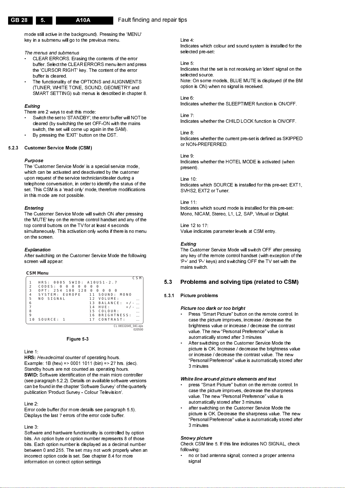
GB 28 A10A5.
mode still active in the background). Pressing the 'MENU'
key in a submenu will go to the previous menu.
The menus and submenus
• CLEAR ERRORS. Erasing the contents of the error
buffer. Select the CLEAR ERRORS menu item and press
the 'CURSOR RIGHT' key. The content of the error
buffer is cleared.
• The functionality of the OPTIONS and ALIGNMENTS
(TUNER, WHITE TONE, SOUND, GEOMETRY and
SMART SETTING) sub menus is described in chapter 8.
Exiting
There are 2 ways to exit this mode:
• Switch the set to 'STANDBY',the error buffer will NOT be
cleared (by switching the set OFF-ON with the mains
switch, the set will come up again in the SAM).
• By pressing the 'EXIT' button on the DST.
5.2.3 Customer Service Mode (CSM)
Purpose
The 'Customer Service Mode' is a special service mode,
which can be activated and deactivated by the customer
upon request of the service technician/dealer during a
telephone conversation, in order to identify the status of the
set. This CSM is a 'read only' mode, therefore modifications
in this mode are not possible.
Entering
The Customer Service Mode will switch ON after pressing
the 'MUTE'key on the remote control handset and any of the
top control buttons on the TV for at least 4 seconds
simultaneously. This activation only worksifthere is no menu
on the screen.
Explanation
After switching on the Customer Service Mode the following
screen will appear:
CSM Menu
1 HRS: 0005 SWID: A10US1-2.7
2 CODES: 0 0 0 0 0 0 0
3 OPT: 254 100 128 0 0 0 0 0
4 SYSTEM: EUROPE 11 SOUND: MONO
5 NO SIGNAL 12 VOLUME:
6 13 BALANCE: +/7 14 HUE: +/8 15 COLOUR:
9 16 BRIGHTNESS:
10 SOURCE: 1 17 CONTRAST:
Figure 5-3
Line 1:
HRS:
Hexadecimal
Example: 1B (hex) => 0001 1011 (bin) => 27 hrs. (dec).
Standby hours are not counted as operating hours.
SWID:
Software identification of the main micro controller
(see paragraph 5.2.2). Details on available software versions
can be found in thechapter 'Software Survey' of the quarterly
publication 'Product Survey - Colour Television'.
Line 2:
Error code buffer (for more details see paragraph 5.5).
Displays the last 7 errors of the error code buffer.
Line 3:
Software and hardware functionality is controlled by option
bits. An option byte or option number represents 8 of those
bits. Each option number is displayed as a decimal number
between 0 and 255. The set may not work properly when an
incorrect option code is set. See chapter 8.4 for more
information on correct option settings
counter of operating hours.
Fault finding and repair tips
CSM
CL 06532045_041.eps
5.3 Problems and solving tips (related to CSM)
5.3.1 Picture problems
Line 4:
Indicates which colour and sound system is installed for the
selected pre-set:
Line 5:
Indicates that the set is not receiving an 'ident' signal on the
selected source.
Note: On some models, BLUE MUTE is displayed (if the BM
option is ON) when no signal is received.
Line 6:
Indicates whether the SLEEPTIMER function is ON/OFF.
Line 7:
Indicates whether the CHILD LOCK function is ON/OFF.
Line 8:
Indicates whether the current pre-set is defined as SKIPPED
or NON-PREFERRED.
Line 9:
Indicates whether the HOTEL MODE is activated (when
present).
Line 10:
Indicates which SOURCE is installed for this pre-set: EXT1,
SVHS2, EXT2 or Tuner.
Line 11:
Indicates which sound mode is installed for this pre-set:
Mono, NICAM, Stereo, L1, L2, SAP, Virtual or Digital.
Line 12 to 17:
Value indicates parameter levels at CSM entry.
Exiting
The Customer Service Mode will switch OFF after pressing
any key of the remote control handset (with exception of the
'P+' and 'P-' keys) and switching OFF the TV set with the
mains switch.
Picture too dark or too bright
• Press “Smart Picture” button on the remote control. In
case the picture improves, increase / decrease the
brightness value or increase / decrease the contrast
value. The new “Personal Preference” value is
automatically stored after 3 minutes
• After switching on the Customer Service Mode the
picture is OK. Increase / decrease the brightness value
or increase / decrease the contrast value. The new
“Personal Preference” value is automatically stored after
3 minutes
White line around picture elements and text
• press “Smart Picture” button on the remote control. In
case the picture improves, decrease the sharpness
value. The new “Personal Preference” value is
automatically stored after 3 minutes
• after switching on the Customer Service Mode the
picture is OK. Decrease the sharpness value. The new
“Personal Preference” value is automatically stored after
3 minutes
Snowy picture
Check CSM line 5. If this line indicates NO SIGNAL, check
following:
• no or bad antenna signal; connect a proper antenna
signal
Page 29
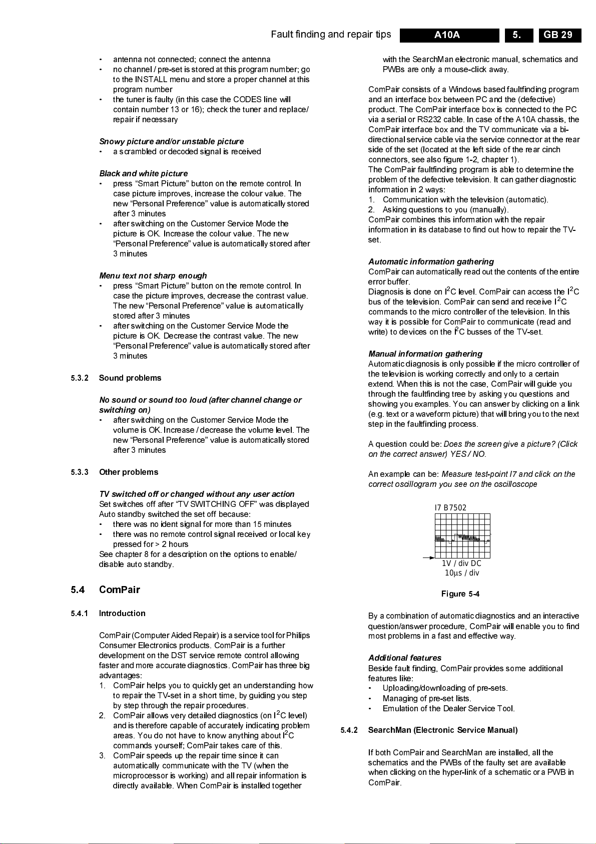
Fault finding and repair tips
GB 29A10A 5.
• antenna not connected; connect the antenna
• no channel / pre-set is stored at this program number; go
to the INSTALL menu and store a proper channel at this
program number
• the tuner is faulty (in this case the CODES line will
contain number 13 or 16); check the tuner and replace/
repair if necessary
Snowy picture and/or unstable picture
• a scrambled or decoded signal is received
Black and white picture
• press “Smart Picture” button on the remote control. In
case picture improves, increase the colour value. The
new “Personal Preference” value is automatically stored
after 3 minutes
• after switching on the Customer Service Mode the
picture is OK. Increase the colour value. The new
“Personal Preference” value is automatically stored after
3 minutes
Menu text not sharp enough
• press “Smart Picture” button on the remote control. In
case the picture improves, decrease the contrast value.
The new “Personal Preference” value is automatically
stored after 3 minutes
• after switching on the Customer Service Mode the
picture is OK. Decrease the contrast value. The new
“Personal Preference” value is automatically stored after
3 minutes
5.3.2 Sound problems
No sound or sound too loud (after channel change or
switching on)
• after switching on the Customer Service Mode the
volume is OK. Increase / decrease the volume level. The
new “Personal Preference” value is automatically stored
after 3 minutes
with the SearchMan electronic manual, schematics and
PWBs are only a mouse-click away.
ComPair consists of a Windows based faultfinding program
and an interface box between PC and the (defective)
product. The ComPair interface box is connected to the PC
via a serial or RS232 cable.In case of the A10A chassis, the
ComPair interface box and the TV communicate via a bi-
directional service cable via the service connector at the rear
side of the set (located at the left side of the rear cinch
connectors, see also figure 1-2, chapter 1).
The ComPair faultfinding program is able to determine the
problem of the defective television. It can gather diagnostic
information in 2 ways:
1. Communication with the television (automatic).
2. Asking questions to you (manually).
ComPair combines this information with the repair
information in its database to find out how to repair the TV-
set.
Automatic information gathering
ComPair can automatically readoutthe contents of the entire
error buffer.
Diagnosis is done on I
bus of the television. ComPair can send and receive I
2
C level. ComPair can access the I2C
2
C
commands to the micro controller of the television. In this
way it is possible for ComPair to communicate (read and
write) to devices on the I
2
C busses of the TV-set.
Manual information gathering
Automatic diagnosis is only possible if the micro controller of
the television is working correctly and only to a certain
extend. When this is not the case, ComPair will guide you
through the faultfinding tree by asking you questions and
showing you examples. You can answer by clicking on a link
(e.g. textor a waveformpicture) that will bring you to the next
step in the faultfinding process.
A question could be:
Does the screen give a picture? (Click
on the correct answer) YES / NO.
5.3.3 Other problems
TV switched off or changed without any user action
Set switches off after “TV SWITCHING OFF” was displayed
Auto standby switched the set off because:
• there was no ident signal for more than 15 minutes
• there was no remote control signal received or local key
pressed for > 2 hours
See chapter 8 for a description on the options to enable/
disable auto standby.
5.4 ComPair
5.4.1 Introduction
ComPair (Computer Aided Repair) is a service toolforPhilips
Consumer Electronics products. ComPair is a further
development on the DST service remote control allowing
faster and more accurate diagnostics. ComPair has three big
advantages:
1. ComPair helps you to quickly get an understanding how
to repair the TV-set in a short time, by guiding you step
by step through the repair procedures.
2. ComPair allows very detailed diagnostics (on I
and is therefore capable of accurately indicating problem
areas. You do not have to know anything about I
commands yourself; ComPair takes care of this.
3. ComPair speeds up the repair time since it can
automatically communicate with the TV (when the
microprocessor is working) and all repair information is
directly available. When ComPair is installed together
2
C level)
2
C
An example can be:
Measure test-point I7 and click on the
correct oscillogram you see on the oscilloscope
I7 B7502
1V / div DC
10µs / div
Figure 5-4
By a combination of automatic diagnostics and an interactive
question/answer procedure, ComPair will enable you to find
most problems in a fast and effective way.
Additional features
Beside fault finding, ComPair provides some additional
features like:
• Uploading/downloading of pre-sets.
• Managing of pre-set lists.
• Emulation of the Dealer Service Tool.
5.4.2 SearchMan (Electronic Service Manual)
If both ComPair and SearchMan are installed, all the
schematics and the PWBs of the faulty set are available
when clicking on the hyper-link of a schematic or a PWB in
ComPair.
Page 30
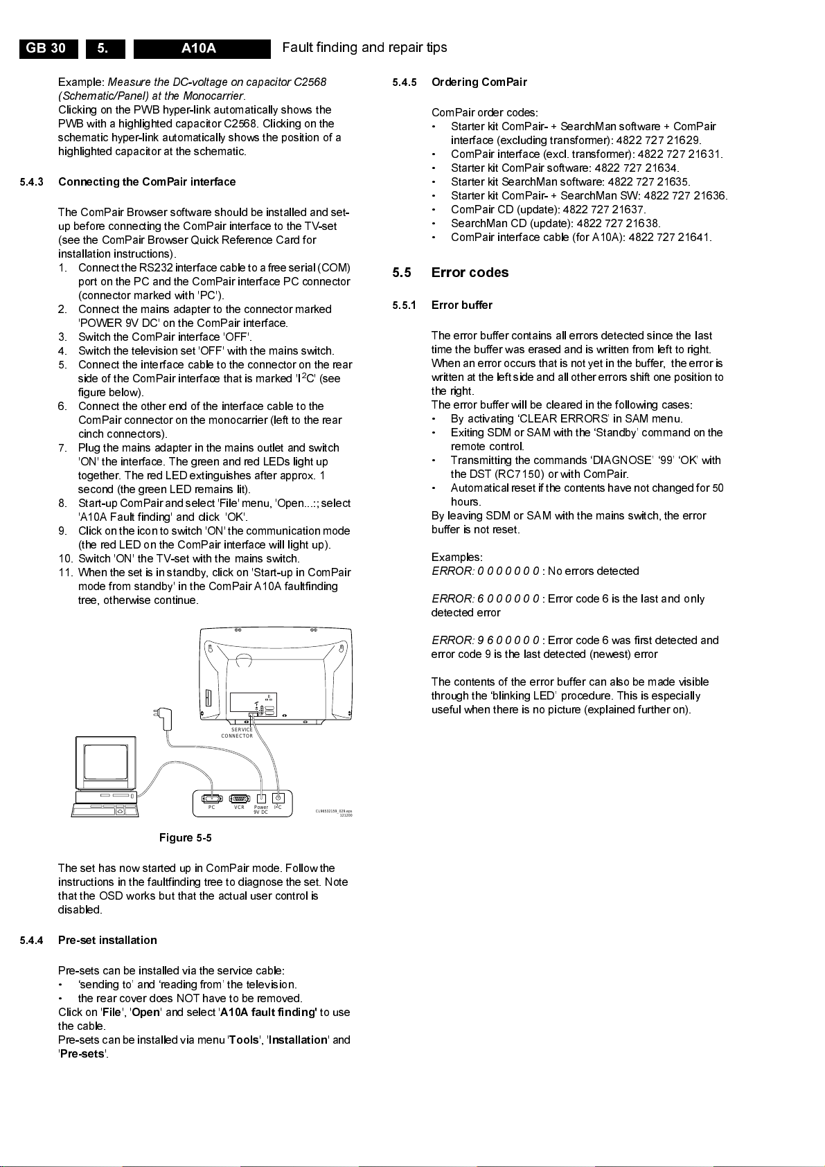
GB 30 A10A5.
Fault finding and repair tips
Example:
Measure the DC-voltage on capacitor C2568
(Schematic/Panel) at the Monocarrier.
Clicking on the PWB hyper-link automatically shows the
PWB with a highlighted capacitor C2568. Clicking on the
schematic hyper-link automatically shows the position of a
highlighted capacitor at the schematic.
5.4.3 Connecting the ComPair interface
The ComPair Browser software should be installed and set-
up before connecting the ComPair interface to the TV-set
(see the ComPair Browser Quick Reference Card for
installation instructions).
1. Connect the RS232 interface cable toafreeserial (COM)
port on the PC and the ComPair interface PC connector
(connector marked with 'PC').
2. Connect the mains adapter to the connector marked
'POWER 9V DC' on the ComPair interface.
3. Switch the ComPair interface 'OFF'.
4. Switch the television set 'OFF' with the mains switch.
5. Connect the interface cable to the connector on the rear
side of the ComPair interface that is marked 'I
figure below).
6. Connect the other end of the interface cable to the
ComPair connector on the monocarrier (left to the rear
cinch connectors).
7. Plug the mains adapter in the mains outlet and switch
'ON' the interface. The green and red LEDs light up
together. The red LED extinguishes after approx. 1
second (the green LED remains lit).
8. Start-up ComPairand select 'File' menu, 'Open...:; select
'A10A Fault finding' and click 'OK'.
9. Click on the iconto switch 'ON' the communication mode
(the red LED on the ComPair interface will light up).
10. Switch 'ON' the TV-set with the mains switch.
11. When the set is in standby, click on 'Start-up in ComPair
mode from standby' in the ComPair A10A faultfinding
tree, otherwise continue.
2
C' (see
5.4.5 Ordering ComPair
ComPair order codes:
• Starter kit ComPair- + SearchMan software + ComPair
interface (excluding transformer): 4822 727 21629.
• ComPair interface (excl. transformer): 4822 727 21631.
• Starter kit ComPair software: 4822 727 21634.
• Starter kit SearchMan software: 4822 727 21635.
• Starter kit ComPair- + SearchMan SW: 4822 727 21636.
• ComPair CD (update): 4822 727 21637.
• SearchMan CD (update): 4822 727 21638.
• ComPair interface cable (for A10A): 4822 727 21641.
5.5 Error codes
5.5.1 Error buffer
The error buffer contains all errors detected since the last
time the buffer was erased and is written from left to right.
When an erroroccurs that is not yet in the buffer, the error is
written at the left side and all other errors shift one position to
the right.
The error buffer will be cleared in the following cases:
• By activating ‘CLEAR ERRORS’ in SAM menu.
• Exiting SDM or SAM withthe ‘Standby’ command on the
remote control.
• Transmitting the commands ‘DIAGNOSE’ ‘99’ ‘OK’ with
the DST (RC7150) or with ComPair.
• Automatical reset if thecontents have not changed for 50
hours.
By leaving SDM or SAM with the mains switch, the error
buffer is not reset.
Examples:
ERROR:0000000
ERROR:6000000
detected error
: No errors detected
: Error code 6 is the last and only
AUDIO EXTERNAL 1
SERVICE
CONNECTOR
PC VCR I2CPower
9V DC
Figure 5-5
The set has now started up in ComPair mode. Follow the
instructions in the faultfinding tree to diagnose the set. Note
that the OSD works but that the actual user control is
disabled.
5.4.4 Pre-set installation
Pre-sets can be installed via the service cable:
• ‘sending to’ and ‘reading from’ the television.
• the rear cover does NOT have to be removed.
Click on '
File
', '
Open
' and select '
A10A fault finding'
the cable.
Pre-sets can be installed viamenu '
'
Pre-sets
'.
Tools
EXTERNAL 2
L
R
', '
Installation
CL96532159_029.eps
121200
to use
'and
ERROR:9600000
: Error code 6 was first detected and
error code 9 is the last detected (newest) error
The contents of the error buffer can also be made visible
through the ‘blinking LED’ procedure. This is especially
useful when there is no picture (explained further on).
Page 31

Fault finding and repair tips
GB 31A10A 5.
5.5.2 Error codes
If possible check the entire content of the error buffers. In
some situations an error code is only the result of another
In case of non-intermittent faults, clear the error buffer before
starting the repair, this to prevent that ‘old’ error codes are
present.
error code (and not the actual cause).
Note:
a fault in the protection detection circuitry can also lead
to a protection.
Error code Error description Possible defective components
0 No error detected -
1 EW and/or High beam protection active LOT, Line deflection circuit, EW-circuit or CRT amplifier cir-
cuit, picture tube or +200V missing
2 Vertical protection Vertical circuit is defective
3 X-ray protection active USA only
4 5V protection active +5V supply line is low or short circuit
5 Reserved -
2
6 General I
C bus error I2C-bus short- or open circuit on uP
7 BC-loop not stabilised RGB amplifiers, RGB guns or RGB driving signals of BOCMA
2
8 BOCMA - I
C error item 7301 on diagram C1 (IC TDA888x)
9 BOCMA 8V supply failure item 7301 on diagram C1 and/or R3331
2
10 NVM I
C error item 7066 on diagram C3 (IC M24C32)
11 NVM identification failure item 7066 on diagram C3 (IC M24C32)
12 uProcessor internal RAM test failure item 7064 on diagram C3 (IC SAA5667)
2
13 Main Tuner - I
14 Sound processor - I
C error Item 1225 on diagram A4 (UV13xx)
2
C error item 7651 on diagram C5 (IC MSP34xxx)
15 SRAM test error item 7070 on diagram C4 (IC UPD431000A)
2
16 Second Tuner - I
2
17 PIP IC I
C error or DW IC - I2C error item 7803 on diagram L2 (USA only) or 7801 on diagram F1
18 I/O expander IC- I
19 Guide
+-I2
20 V-chip for PIP - I
21 NV clock - I
C error Item 1900 on diagram L1 (USA only) or 7201 on diagram F2
2
C error item 7910 on diagram L1 (USA only) or 7403 on diagram F3
C error item 7005 on diagram K1 (IC LC27016B) - USA only
2
C error item 7501 on diagram F5 (IC Z86130) - USA only
2
C error item 7011 (IC MK41T56) - LATAM only
22 Reserved -
2
23 Second BOCMA IC on DW panel - I
C error item 7301 on diagram F4 (IC TDA888x)
Explanation of the error codes:
Error 0
No error
Error 1
Set is switched to protection; error code 1 is placed in the
error buffer; the LED will blink 1 time (repeatedly). If this
happens, isolate each circuit to determine the cause:
• EW protection - PROT-UP
If this protection is active,the causes could be one of the
following;
• bad contacts of:
– horizontal deflection coil
– linearity coil 5417
– S-correction capacitor 2418/2419
– flyback capacitor 2414/2416
– line output stage
• short circuit of:
• flyback diode 6414
• EW transformer (bridge coil) 5478/5479 or 5474/
5475/5476 (version dependent)
• EW driver 7470
• High beam current protection - IBeam
As the name implies, the cause of this protection is a too
high beam current (bright screen with flyback lines).
Check whether the +200 V supply to the CRT panel is
present. If the voltage is present, the most likely cause is
the CRT panel or the picture tube. Disconnect the CRT
panel to determine the cause. Ifthe +200 V voltage is not
present, check R3840 at the CRT-panel and R3445 &
D6445 at the main panel.
Error 2
If this protection is active, the cause could be one of the
following (most likely in the vertical output stage):
• 7501 is faulty.
• poor contact or open circuit of deflection coil.
• +13V-VERT and/or -13V not present.
Error 3
X-Ray protection - PROTN
If this protection is active, the most likely cause is the LOT.
Detection via pin 3 of the BOCMA (7301) AND pin 5 of theµP
(7064)
Error 4
The 5V-protection active and error code 4 is placed in the
error buffer. The LED will blink 4 times (repeatedly).
A 5 V failure can cause a drop in the 5 V supply output,
resulting in an undefined behaviour of the set. Therefore, all
2
C devices connected to the 5V-supply are constantly
I
monitored. When none of these devices respond to the micro
controller for a prolonged time, the micro controller assumes
that there is a failure in the 5V-supply.
Page 32

GB 32 A10A5.
Fault finding and repair tips
By starting up the set with the service jumpers shorted, the
5V-protection is disabled and it is easier to determine the
cause. +5V protection will be activated when these I
devices fail (no I
2
C communication):
2
C
• Main Tuner 1125 on main panel.
• ITT sound processor MSP34xx (7064) on the SSB.
The following tips are useful to isolate the problem area after
overriding the +5V-protection. Determine whether:
1. The +5V sourceisworking properly; isolate coil 5430 and
jumper 9044 and measure the +5V.
2. ITT sound processor circuit is loading the +5V; isolate
coil 5430.
3. The tuner is loading the +5V source; isolate jumper 9044.
4. Main tuner circuit is loading the +5V source; isolate coil
5261.
Caution!
Overriding the 5V-protection when there is a 5V
failure can increase the temperature in the set and may
cause permanent damage to components. Do not override
the 5V-protection for a prolonged time.
Error 5
Reserved.
Error 6
This will occur in the following cases:
• SCL or SDA is shorted to ground.
• SCL is shorted to SDA.
• SDA or SCL connection at the micro controller is open
circuit.
Error 16
PIP/DW Tuner I
2
C error. The tuner (TEDE9 - item 7201) on
DW-panel does not respond to the micro controller.
Error 17
2
PIPICI
C failure (item 7801) or Double Window IC I2C
failure.
Error 18
I/O expander IC I
2
C failure (item 7910 on PIP panel or item
7403 on DW panel).
Error 19
2
Guide+ I
Error 20
V-chip IC I
Error 21
NV clock IC I
C failure (item 7005). Only for USA.
2
C failure. Only for USA.
2
C failure at mono board (item 7011). Only for
LATAM.
Error 22
Reserved.
Error 23
2nd BOCMA IC (item 7301on DW panel) I
2
C communication
failure.
Error 24 - 29
Reserved.
Error 7
Black current loop instability protection.
The possible cause could be a defect in one or more of the
RGB amplifiers, RGB guns or RGB driving signals. The
detection is via the black current feedback loop to pin 30 of
the BOCMA (item 7301).
Error 8
BOCMA (item 7301 on SSB) is corrupted, the I
2
Clinetothe
BOCMA is low or no supply voltage is present at pin 14 and/
or pin 60 (3V3).
Error 9
No supply voltage at pin 53. Check NFR 3331and coil 5333.
Error 10
NV memory (EEPROM - item 7066) does not respond to the
micro controller.
Error 11
During the last start-up, the NVM and the micro controller did
not recognize each other (e.g. one of them was replaced or
the NV memor y has been changed, adapted or lost).
Therefore the NVM was loaded with default values.
Error 12
Microprocessor (Painter - item 7064) internal RAM test
failure.
Error 13
Tuner (item1225) is corrupted, theI
2
C line to the tuner is low
or no supply voltage at pin 6, 7 or 9 of the tuner.
Note:
Error codes 1, 2 and 4 are protections, so in these
cases, the voltage supply to some circuits will be switched
off. Also the LED will blink the number of times equivalent to
the most recent error code.
5.6 The 'blinking LED' procedure
The contents of the error buffer can also be made visible
through the 'blinking LED' procedure. This is especially
useful when there is no picture.
When the SDM is entered, the LED will blink the contents of
the error-buffer. Error-codes≥10 are shown as follows:
A long blink of 750 msec. which is an indication of the
decimal digit, followed by a pause of 1500 msec, followed by
n short blinks.
When all the error-codes are displayed, the sequence is
finished with a LED display of 3 seconds. Then the sequence
starts again.
Example:
Error code position 1 2 3 4 5
Error buffer: 12 9 6 0 0
After entering SDM: 1 long blink (750 ms) - pause (1.5 s) - 2
short blinks - pause (3 s) - 9 short blinks - pause (3 s) - 6
short blinks - pause (3 s) - long blink (3 s) - etc.
Note:
If errors 1, 2 or 4 occur, the LED
occurred error, even if the set is NOT in service mode.
always
gives the last
Error 14
Sound controller MSP34xx does not respond to the micro
controller.
Error 15
SRAM IC test failure (item 7070).
Page 33

Fault finding and repair tips
GB 33A10A 5.
5.7 Repair tips
In this paragraphsometrouble shooting tips for the deflection
and power supply circuitry are described.
5.7.1 The deflection circuit
Measure if the V
2939 and/or 2940 (diagram A1).
If the voltage is not present, disconnect jumpers 9936 and
9937. The whole ‘Line Deflection’ stage is now disconnected.
If the voltage is present thenthe problem might be causedby
the deflection circuit. Either transistor 7410 is defective or the
driver circuit around transistor 7481 is faulty or the ‘horizontal
drive’ signal coming from the BOCMA IC 7301-pin 56 on the
SSB is missing.
Note:
• When you short the collector and emittor of transistor
7410, hickup noise can be heard from the power supply
circuit.
• To determine whether the fault is caused by the line
deflection circuit (diagram A2) or by the E/W circuit
(present when screen size > 21”), insert jumper into
position number 9409 (in this case the E/W protection is
disabled).
If the basic deflection is working (picture is parabolic
distorted), the fault must be searched for in the E/W
circuit. If there is no horizontal deflection, the fault must
be searched for in the deflection circuit.
• If any of the protection circuits in the ‘Line output’ stage
are activated, the set will shut down. Depending on the
protections, the LED will blink according to the fault
defined.
In order to determine which protection circuit is active,
isolation of circuits is necessary.
These protection circuits are:
• High beam protection, see error 1.
• X-ray protection, see error 1.
• If the ‘High beam’- or ‘X-ray’ protection is active, the set
will go to protection and the SDM will be activated.
The ‘service LED’ blinks repetitively 1 time.
If this happens, isolate each circuit to determine the
cause.
(140 V) is present across components
BAT
If not, check components D6938, C2939 and C2940 and
L5941.
If they are OK, check the voltage at pin 3 of IC 7942.
If this voltage is not present, check fuse 1941 and fuse 1942.
If the voltage is present at pin 3, replace opto-coupler 7929.
Another way to confirm whether the OVP is active, is to
measure the voltage with an oscilloscope at IC7902 pin 4.
If the voltage is fluctuating between 11 and 14 V, then check
the components as described above.
5.7.2 The power supply
To trouble shoot the A10 SMPS, first check the +5V_STBY
voltage on item 7968-pin 3 and 4. If this voltage is not
present, check fuse 1961 and diode 6961.
If they are working properly, the problem might be caused by
the circuit on the primary side of the switching transformer.
Check in this case the output of the bridge diodes at the
cathode of diode 6912, 6913 or 6915 for approximately 300
Vdc.
If this voltage is missing, check the bridge diodes and the
fuse. If fuse 1900 is blown, measure IC7921 (diagram A1)
between pins 3 and 2 to make sure that there is no short
circuit present.
If the 300 Vdc is present on pin 3 of IC7902, check for a start-
up voltage of 16 V on pin 4 of IC7921. If this voltage is not
present, check if R3914 is open (a short circuit between pin
4 and 5 will also cause this problem). It is necessary, for the
power supply, to have a feedback signal from the hot
secondary side of the switch mode transformer (T5912-pin 8
and 9) to oscillate.
If this start-up voltage is present on pin 4 of IC7902 and the
supply is not oscillating, check R3929 and D6929.
The A10 power supply has been designed with an Over
Voltage Protection (OVP). To determined whether the OVP
is active, check whether V
pin 1.
(141 V) is present at IC7971
BAT
Page 34

GB 34 A10A5.
Personal notes:
Fault finding and repair tips
Page 35

&
Alignments
GB 77A10A 8.
Note: The Service Default Mode (SDM) and Service
Alignment Mode (SAM) are described in chapter 5.
8.1 General alignment conditions
All electrical adjustments should be performed under the
following conditions:
• Supply voltage: 110 / 220 V (±10%);50/60Hz(±5%)
• Warm-up time:≈20 minutes
• The voltages and oscillograms are measured in relation
to the tuner earth (with exception of the voltages on the
primary side of the power supply).Never use the cooling
fins / plates as ground.
• Test probe: Ri > 10 MΩ; Ci < 2.5 pF.
• Use an
isolated
trimmer / screwdriver for the alignments.
8.2 Electrical alignments
8.2.1 Vg2
Rough alignment
Using a pattern-generator displaying a black pattern.
1. Set brightness and contrast to minimum in a black room
(OSD still visible). Select any of the AV-sources.
2. Go to the SAM.
3. Set VSD to ON.
4. Adjust Vg2 potmeter of LOTuntilthe horizontal line is just
visible.
5. Set VSD to OFF.
6. Exit SAM.
Fine adjustment
1. Activate the SAM-menu (see chapter 5.2.2). Go to the
sub-menu 'WHITE TONE' and adjust the value of
NORMAL RED, GREEN and BLUE to 40 (or 42 for 29”
RF)
2. Go, via the MENU key, temporarely to the normal user
menu and set the values of BRIGHTNESS and
CONTRAST to 0.
3. Return to the SAM-menu via theMENU-key. Disable the
black current loop by changing ‘AKB’ to ‘OFF’.
4. Connect the RF-output of the pattern generator to the
antenna-input. Test pattern is a 'black' pattern (blank
screen on CRT
Set the time base of the oscilloscope to 0.5 ms with
external triggering on the vertical pulse. Measure the
black level pulse during the vertical flyback at the RGB
cathodes of the CRT.
without
any OSD info).
8.2.2 Focus
1. Tune the set toa circle or crosshatch test pattern (use an
external video pattern generator).
2. Adjust the 1st Focus potmeter (upper LOT potmeter)until
the horizontal and vertical lines at 1/4 from east and
west, at the height of the centre line, are of minimum
width without visible haze.
3. Adjust the 2nd Focus potmeter (middle LOT potmeter)
until the horizontal and vertical lines at 1/4 from northand
south, at the height of the centre line, are of minimum
width without visible haze.
Note:
For sets without Double Astigmatic Focus (DAF)panel, there
is only one Focus-potmeter on the LOT.
Adjust according to paragraph 8.2.2 point 2.
8.3 Alignments and settings in the SAM.
8.3.1 General
With the software alignments of the Service Alignment Mode
the Geometry, White tone and Tuner (IF) can be aligned. Put
the set in the SAM mode. The SAM menu will now appear on
the screen (see chapter 5).
Menu navigation is done with the 'CURSOR UP, DOWN,
LEFT or RIGHT' keys of the RC-handset.
8.3.2 Geometry
The geometry alignments menu contains several items to
align the set, in order to obtain a correct picture geometry.
In widescreen sets, the ‘GEOMETRY SW’ menu is available
for separate alignments of the superwide (panorama) mode.
East/West Trapezium
Horizontal Parallel
max.
0V Ref.
Adjust V
cutoff
potmeter of the LOT) to 165 V
V
CUTOFF
Figure 8-1
of the highest of the three guns (with the Vg2
[VDC]
.
DC
CL 06532130_014.eps
131000
Horizontal Bow
Figure 8-2
CL 96532156_012.eps
190101
Page 36

GB 78 A10A8.
Alignments
Initial set-up
1. Connect an external video pattern generator (PAL-
475.25 MHz or NTSC-63.25 MHz) to the aerial input of
the TV-set with a cros shatc h t est pattern.
2. Set 'Smart Picture' to NATURAL.
3. Activate the SAM-menu (see chapter 5).
4. Go to sub-menu GEOMETRY. Now the following
alignments can be performed (dependent on execution):
Service blanking (SERV. BLK)
Switch the blanking of the lower half of the screen ON/OFF
(to be used in combination with the vertical slope alignment).
Vertical slope (VER. SLOPE)
Align the vertical centre of the picture to the verticalcentre of
the CRT.This is the first alignment to be performed of the
vertical alignments. For an easy alignment set SERV.BLK to
ON.
Vertical S-correction (VER. SCOR)
Align the vertical linearity, meaning that verticalintervals of a
grid-pattern must be equal over the entire height.
Vertical amplitude (VER. AMPL)
Align the picture height so that the complete test pattern is
visible. Note that other vertical alignments are not
compensated.
Vertical shift (VER. SHIFT)
Align the vertical centering so that the test pattern is located
vertically in the middle. Repeat the 'vertical amplitude'
alignment if necessary.
Horizontal shift (HOR. SHIFT)
Align the horizontal centre of the picture to the horizontal
centre of the CRT.
Horizontal parallelogram (HOR. PARALLEL)
Align straight vertical lines in the top and the bottom; vertical
rotation around the centre.
East West width (EW. WIDTH)
Align the picture width until the complete test pattern is
visible.
East West Upper Corner (EW. UCORN)
Align straight vertical linesin the upper corners of the screen.
East West Lower Corner (EW. LCORN)
Align straight vertical lines in the lower corners of the screen.
East West Trapezium (EW. TRAP)
Align straight vertical lines in the middle of the screen.
East West parabola (E W. PARA)
Align straight vertical lines at the sides of the screen.
Horizontal bow (HOR. BOW)
Align straight horizontal lines in the top and the bottom;
horizontal rotation around the centre.
8.3.3 Tuner (Large Sig nal Panel and Doub le Window)
IF PLL OFFSET and AFC WINDOW
No adjustments needed for these alignments. The default
values for these options are:
– IF PLL OFFSET: 32
– AFC WINDOW: 100 kHz
AGC
Set an external pattern generator (e.g. PM5418) to a grey
scale video signal and connect it to the aerial input with RF
signal. Set the signal amplitude to at least 1 mV and to a
frequency of 475.25 MHz for PAL or 63.25 MHz for NTSC.
– Activate the SAM-menu. Go to the sub-menu TUNER,
select the sub-menu option AFC WINDOW and adjust
the value to 100kHz.
– Select the AGC sub-menu
– Connect a DC multi-meter to pin 1 of the tuner 1225
(LSP) or 7200 (DW).
– Adjust the AGC until the voltage at pin 1 of the tuner is
within 2.5 V < AGC takeover voltage < 3.8 V
– The value can be incremented or decremented by
pressing the RIGHT/LEFT cursor keys on the RC.
– Switch the set to standby.
8.3.4 White tone
In the WHITE TONE s ub m enu, t h e colour values for the
colour temperature values can be changed.
The colour temperature mode (NO RMA L, DELTA COOL,
DELTA WARM) or the colour (R, G, B) can be selected w ith
the UP/DOWN cursor keys. The mode or value can be
changed with the RIGHT/LEFT cursor keys.
First the values for the NORMAL colour temperature should
be selected. Then the offset values for the DELTA COOL and
DELTA WARM mode can be selected. Note that the
alignment values are non-linear
0 represents the middle value (no offset difference).
• +1 to +63 represent a positive offset (63is the maximum
positive offset).
• -63 to -1 represent a negative offset (-63 is the minimum
negative offset).
8.4 Options
8.4.1 Introduction
Options are used to control the presence/absence of certain
features and hardware. The correct option values can be
found on a sticker on the picture tube (after removal of the
rear cover).
There are two ways to change the option settings (see also
chapter 5):
1. Changing a single option:
An option can be selected with the MENU UP/DOWN
keys and its setting can be changed with the MENU
LEFT/RIGHT keys.
2. Changing multiple options by changing Option Bytes:
Changing the option bytes directly, makes it possible to
set all options very fast. An option byte (OB1..8) can be
selected with the MENU UP/DOWN keys and its setting
can be changed with the MENU LEFT/RIGHT keys. An
option byte represents a number of different options. All
options are controlled via 8 option bytes. Select the
option byte (OB1..OB8) and key in the new value.
Note:
Changes in the option byte settings are saved by selecting
STORE and pressing theMENU RIGHT key. All changes are
disregarded w hen the OPTION submenu is left w ithout using
the STORE comm and.
Some changes will only take affect after the set has been
switched OFF and ON with the mains switch (cold start).
8.4.2 List of options
In the table below an overview is given of the possible options
(in alphabetical order).
These option b i t s can be set O N (= 1) or OFF (= 0). If an
option is set ON, it represents a certain value.
To calculate the Option Byte value (OB), add the values of
the 8 option bits (see 8.4.3).
Page 37

Option abbreviation Feature description
AAVL Automatic Volume Level
APC Auto Picture Control
ASBY Auto sw itch to STDBY after 2 hrs.
AUSB Auto sw itch to STD BY after 2 hrs.
AV3 External 3 (Side I/O)
BLMU Blue Mute
C169 Picture setting for Compress 16:9
CBFL Comb Filter
CCAP Closed Captioning
CHLK Child Lock
CHNA China
CVI Ext. source selectionfor DW/PIP
DNRM DNR Noise Reduction
DTXT Dual page Teletext available
E149 Picture setting for Expand 14:9
FAPG Favorite Page
HOSP Hospitality mode
INCF Internal Comb Filter
IPIX Incredible Picture
IPMU Incredible Picture via menu
ISUR Incredible Surround
MLNK M-Link
NTSC NTSC playback
NVM Power down circuit to protect NVM
PIPC PIP Control
PIPS PIP Surf
PIPT PIP Tuner
PLST Program List
ROTI Rotation
SBNP Auto Standby with no picture
SMCK Smart clock
SNIC Sound IC 3451
SOSD Smart OSD
SURF Surf
TIME Timer
TWIN T ime Window
VDBY Virtual Dolby
VMUT Video Mute
VSLC Vertical Slicing
W169 Double Window 16:9
W4X3 Double Window 4:3
Alignments
GB 79A10A 8.
8.4.3 Option bits/bytes
An option byte value is calculated in the following way:
Value 'option bit 1' x 1 =
Value 'option bit 2' x 2 =
Value 'option bit 3' x 4 =
Value 'option bit 4' x 8 =
Value 'option bit 5' x 16 =
Value 'option bit 6' x 32 =
Value 'option bit 7' x 64 =
Value 'option bit 8' x 128 =
====================== +
Total value 'option byte' =
Page 38

GB 80 A10A9.
Circuit descriptions and abbreviation list
' ((
9.1 Circuit descriptions
The following circuits are described:
1. Introduction
2. Block diagram
3. Power supply (see A8 TM: 4822 727 21613)
4. Control
5. Tuner & IF
6. Video processing
7. Synchronisation
8. Horizontal deflection (see A8 TM: 4822 727 21613)
9. Vertical deflection (see A8 TM: 4822 727 21613)
10. Audio processing
11. OSD / T eletext
12. CRT / SCAVEM / Rotation
13. Double Window (DW)
9.1.1 Introduction
The A10A is the successor of the A8-chassis. A10 is the
chassis name, A = Asian Pacific.
9.1.2 Block diagram
DOUBLE WINDOW
SPLITTER
F
TUNER2
(DW)
CVBS-2
VIDEO-EXT
CVBS-1
IF
FILTER
VIF
VSIF
BOCMA
Where the A8 used a lot of different panels, the A10
architecture consist of 1 conventional Large Signal Panel
(LSP) and 1 Small Signal Board (SSB) module, placedinto a
so called SIMM-connector (Standard Interface, 80 pins):
• The LSP is built up very conventional, with hardly any
surface mounted components on the copper side. It
incorporates the Power Supply, the Deflection, the
Tuner, the I/O and the Audio Amplifier circuits.
• The SSB is a high tech module (2 sides reflo w
technology, full SMT) with very high component density.
Despite this, it is designed in such a way, that repair on
component level will be pos s i b l e . To achieve this
extensive diagnostic possibilities are provided via
Service Modes and/or ComPair. The SSB incorporates
the IF-, Video / Audio-processing, Control and OSD/TXT
circuits.
In this 'circuit description'chapter, sometimes will be referred
to the Training Manual of the A8 (4822 727 21613). This is
done for the following circuits: the Power supply, the
Horizontal (Line) Deflection and the Vertical (Frame)
deflection parts. The el ec trical princ i p l e of these circuits are
also applicable on the A10.
FBL
YUV
DW
DW
PROC.
YUV-MAIN-OUT
YUV-PIP+MAIN-IN
HISTO
(OPT.)
COMB
(OPT.)
BOCMA
FRAME+
FRAME-
LINE
VERT.
HOR.
VFB
HFB
EXT
I/O
TOP
CONTROL
IR
REC.
EHT
200V
V
+8V
+5V
ETC.
BAT
POWER
ON/OFF
MAINS
POWER
SUPPLY
The Tuner is a PLL t uner and delivers the IF-signal, via audio
& video SAW-filters, to the Multi-system TV processor
(TDA888x, IC7301 also called BO CM A), which has the
following functions:
• Multi-system decoder.
• Video source- and record select.
• Colour decoder.
• RGB output.
TUNER1
(MAIN)
IF
FILTER
Figure 9-1
CVBS-TER-OUT
VIDEO-EXT
MONITOR-OUT
VSIF
PIP-AUDIO
MONITOR-OUT
AUDIO-EXT
E/W
VIF
PAINTER
SIF
RGB-CRT
CVBS-TEXTRGB-TEXT-OSD
(µP)
L/R
MSP
HP
+27V
CRT
SCAVEM
VFB
HFB
NVM
FLASH
(SW)
R
G
+
B
SCAVEM
ACTIVE
SUBWOOFER
E/W
L/R
CL 06532153_022.eps
• Sound demodulator.
• Geometry control.
• Picture improvement.
• Synchronisation.
The BOCMA has 1 input for the intern a l CVBS s ignal and 2
inputs for externalCVBSor Y signals. It has only one Chroma
input so that it is not possible to apply 2 separate Y/C inputs.
The selection is made via the I
2
C-bus.
081200
Page 39

Circuit descriptions and abbreviation list
GB 81A10A 9.
It has 2 independently switchableCVBS outputs for e.g. TXT,
Comb-filter, CVBS-monitor or PIP/DW (optional).
Two AV-connectors (cinch) are used: AV1 is fully equipped
and AV2 is meant for VCR. T he M onitor- out of AV2 can be
used for WYSIWYR (What You See Is What You Record).
Internal video processing is done in the BOCMA with YUV-
signals. It also handles the video control, geometry part and
the insertion of the TXT/OSD RGB-signals. The video part
delivers the RGB signals to the CRT-pan el and the geometry
part delivers the H-drive, V-drive (differential output), and E/
W-drive.
Both deflection circuits are located on the LSP and are driven
by the BOCMA. The horizontal output stage generates also
some supply voltages and the EHT-, focus- and Vg2-
voltages.
Picture In Picture (PIP) and Double Window(DW) are both
optional (PIP is only used in the NAFTA-region).
Double Window (DW) models are always equipped with 2
tuners. The IF signal from the 2nd tuner is processed by a
2nd BOCMA video processor.
For AP, China and LATAM regions, the TV uses one RF-
signal, which is splitted and fed to the main tuner on the LSP.
Due to this construction, the main tuner (on the LSP) always
processes the main picture and the 2nd tuner always
processes the DW picture. If the picture needs to be
swapped, then the tuner RF frequency is swapped, rather
then the 'baseband-signal switching' as done in the NAF T A
region.
The V-chip data slicer is not present in these regions.
The RGB amplifiers on the CRT-panel are integrated in one
IC (TDA6107Q) and are supplied with 200 V from the LOT.
The SCAVEMcircuit modulates transitions of the Luminance
(Y) signal on the horizontal deflection current, giving a
sharper picture.
The sound part is built up around the MSP34xx (Multi-
channel Sound Processor) for IF sound detection, sound
control and source selection. Dolby decoding is also done by
the MSP. Amplification is done via an integrated power
amplifier IC, the AN5277.
The microprocessor, called Painter (SAA55XX, IC7064),
takes care of the set control, error generation and analogue
TXT/OSD input- and output processing.
The Painter, ROM and RAM are supplied with 3.3 V, which is
also present during STANDBY.
The NVM (Non Volatile Memory)is used to store the settings,
the flash-RAM contains the set software and the DRAM
(located inside theµP) is capable for storing 10 Teletext
pages or 100 pages (software version dependent).
The power supply is a Switch Mode Power Supply (SMPS)
with minimum voltage switch. It is a flyback converter with
primary current sensing, secondary voltage sensing and
mains input measuring. It is built around IC7921 (which has
a built-in MOSFET and control circuit) and generates a/o. the
140 V (V
During Standby,the power supplyis switched to a 'low power
) and the 27 V (for the audio part).
BAT
burst mode' via TS7946 and the following burst mode
generator, in order to reduce the power consumption.
A relay is used to switch the degaussing circuit for several
seconds during switching 'ON' of the set.
9.1.3 Power supply (diagram A1)
For a circuit description see A8 Training Manual: 4822 727
21613. Differences with the A8 are:
• Item-numbers are different from theonementioned in the
text.
• Degaussing circuit
• Output voltages
Degaussing circuit (diagram A1: section A1 - D3)
The degaussing circuit is activated whenever the TV set is
turned on. So from normal 'off' to 'on' and from 'stand-by' to
'on' the degaussing circuit is activated. During start-up the
signal LIGHT_SENSOR_VD EG AUS (A4-1) is low. After
start-up of theµP this becomes high for 2 seconds which
forces TS7932 in conduction. Now the coil of the relay is
activated and switch 1931 is closed. The mains voltage is
now connected to the degaussing coil. The degaussing
current passes through the degaussing coil and through PTC
3911 and PTC 3912, which limit the inrush-current.
After these 2 seconds, the signal
LIGHT_SENSOR_VDEG A US goes low , 7900 turns off, the
coil of relay 1931 is de-energised and the 220 V
disconnected from the degaussing coil. During normal
operation, no current passes through the degaussing coil
due to the fact that switch 1931 is opened.
Output voltages
• +8V_UNREG (Input voltage for stabiliser 7942 and
supply voltage for the circuit to activate the degaussing
coil).
• +33V (For Tuner at Mono-carrier and PIP-panel).
Created via R3409 and zenerdiode 6481.
•V
• +8V (BOCMA Supply, Video at SSB). Output voltage
(Battery Voltage for Line Output Stage): +140 V.
BAT
from stabiliser 7942. T his voltage is decreased in
standby to 2.3 V. In standby TS7944 is conducting and
switching R3945 parallel to R3942 and R3947.
• +5V_STBY. This voltage is also present during standby.
If this voltage and +5 V are missing check Fuse 1961. If
the voltage at pin2&5of7968 is present replace 7907.
• +5V (For Tuner, NV_CLOCK, Video at SSB, PIP-panel).
This voltage is disabled when the +13V-VERT is not
present at pin 2 of IC7967. +13V -VERT is generated by
the line-output circuit. So when the line-output circuit is
working correctly the +5V is enabled to start the set.
• +27V (Audio Supply). If this voltage is missing check
D6971/6972 and/or sound-amplifier IC7702.
• 3V3_STBY (µP Supply, NVM, BOCMA supply, Receiver
LED): This voltage is also present during standby. If this
voltage is missing check NFR 3964.
9.1.4 Control (diagram C4)
Micro-processor
The microprocessor (SAA55XX, IC7064 called Painter)
provides:
• Control functions for the TV-set.
• On Screen Display (OSD).
• Teletext functions.
• I/O-ports for I
2
C, RC5, LED, and service modes.
• Error code generation.
For 10 pages TXT-data can be stored internally.
The Non Volatile Memory IC7066 isa4kBversion
M24C32W6.
All ICs in this part are supplied with 3V3, which is also
present during Standby. For this voltage a zenerdiode is
used (D6966).
For stable OSD and TXT, the display is synchronised to the
TV signal processing device by way of horizontaland vertical
sync signals provided by external circuits (HFB and VFB).
From these signals all display timings are derived.
The OSD/TXTRGB-outputs (46/47/48)and fastblanking (52)
are fed to the BOCMA (pins 35 - 38).
Below find the pinning description of the Painter (IC7064).
AC
is
Page 40

GB 82 A10A9.
Circuit descriptions and abbreviation list
Pin Signal Function
1 TILT Generates drive signal for
rotation circuit
2 SEL_SVHS_RR_STAT
US2
Selects Y/C source from
Side or Rear I/O and detects
presence of EXT2 (CVB S) /
4:3 or 16:9
4 STATUS1_PIP -
AFT_PIP-50-60HZ
Detects presence of EXT1
(CVBS) / 4:3 or 16:9
5 KEYBOARD Input line from Top Control
keyboard
6 FRONT_DETE CT Detects presence of Head-
phone at FRONT
13 STAND- BY To switch betw een Standby
and Normal operation
16 SEL_MAI N_F RNT _RR Selects main video source
from Rear or Front
17 COMM_LINE P50 in/output (Easylink)
18 LIGHT -
SENSOR_VDEGAUSS
Activates the degaussing re-
lay at switch on
24 SYS1 Selects Combfilter
25 SYS2 Selects Combfilter
28 ON_OFF_LED LED driver output
31 CVBS2OUT CVBS input for TXT data
32 G_SC1-IN_Y-IN
46 B_TX T _O SD Blue output for OSD/TXT
47 G_TXT_OSD Green output for OSD/TXT
48 R_TX T _OS D Red output for OSD/TXT
52 FBL_T X T _O SD Fast blanking output for TXT
and OSD
52 FBL_SCAVEM Fast blanking output for
SCAVEM
53 HFB H-sync input for stable OSD/
TXT
54 SEL_MAIN_R1R2 Selects main video source
from EXT1 or EXT2
55 VFB V-sync input for stable OSD/
TXT
59 SEL_IF_LL Switches the appropriate
SAW filter for LL'
70 CLOCK12MHz Clock input
76 RC5 Input line from Remote Con-
trol
2
81 SCL Clock output of master I
C
bus
2
82 SDA Data in/out of master I
83 SCL_2 Clock output of NVM I
84 SDA_2 Data in/out of NVM I
C bus
2
C bus
2
C bus
93 AGCuP
96 HIS_OFF To activate the optional His-
togram IC TDA9171
98 SOUND_ENABLE Mutes the audio amplifier
100 PANORAMA Activates 16:9 feature
2222
I
C-busses
In the A10A-chassis with Painter-processor there are two
2
C-busses used:
I
• Hardware I
2
C-bus, used for all IC communication.
• Separate short bus for the Non Volatile Memory (NVM),
to avoid data corruption.
• All factory alignments.
• Last Status items for the customer + a complete factory
recall.
9.1.5 Tuner & IF (diagram A4, C1 & C3)
Tuner
Tuning is done via I
V. This voltage is derived from the V
kΩand a zenerdiode.
2
C. The reference voltage on pin 9 is 33
via a resistor of 68
BAT
Video IF amplifier
The IF-filter is integrated in a SAW (Surface Acoustic Wave)
filter. One for filtering IF-video (1451 or 1454 in case of
system L/L') and one for IF-audio (1455). The type of these
filters is depending on the standard(s) that has to be
received.
The output of the tuner is controlled via an IF-amplifier with
AGC-control. This is a v oltage feedback from pin 7 of the
BOCMA to pin 1 of the tuner. The AGC-detector operates on
top sync and top white level. AGC take-over point is adjusted
via the service alignment mode ’Tuner' - 'AGC’. I f there is too
much noise in the picture, then it could be that the AGC
setting is wrong. The AGC - s e t t i ng could also be mis-aligned
if the picture deforms with perfect signal; the IF-amplifier
amplifies too much.
An (alignment free) PLL carrier regenerator with an internal
VCO demodulates the video signal. This VCO is calibrated
by means of a digital control circuit, w hich uses the clock
frequency of theµP as a reference. The frequency setting for
the various standards (33.4, 33.9, 38.0, 38.9, 45.75 and
58.75 MHz) is realised via the I
2
C-bus.
The AFC output is generated by the digital control circuit of
the IF-PLL demodulator and can be read via the I
The v ideo identification circuit is used to identify the selected
CBVS or Y/C signal.
The IC contains a group delay correction circuit, which can
be switchedbetween the BG and a flat group delay response
characteristic. This has the advantage that in multi-standard
receivers no compromise has to be made for the choice of
the SAW filter. Also the sound trap is integrated. The centre
frequency of the trap can be switched via the I
signal is available on pin 27.
QSS sound circuit
The s ingle reference QSS mixer is realised by a mult iplier. In
this multiplier the SIF signal is converted to the intercarrier
frequency by mixing it with the regenerated picture carrier
from the VCO. The mixer output signal is supplied to the
output via a high-pass filter for attenuation of the residual
video signals. With this system a high performance hi-fi
stereo sound processing can be achieved.
2
C-bus.
2
C-bus. The
NVM
The Non Volatile Memory IC7066 contains all set related
data that must be kept permanently, such as:
• Software identification.
• Operational hours.
• Error-codes.
• Option codes.
Page 41

Circuit descriptions and abbreviation list
9.1.6 Video processing (diagram C2 & C3)
GB 83A10A 9.
R-CRT
G-CRT
B-CRT
EHT-INF
33
35
31
34
18
SDA
17
SCL
IIC BUS
CONTROL
13
HALFT
50
SWO2
22
SWO1
Y
SW OUT
LUM-
RGB
MATRIX
CD
CD
MATRIX
MATRIX
U
RGB-2
Y
DELAY
PEAKING
RGB
R
G
WHITE/
SATURATION
SATURATION
V
INPUT
RGB/YUV
CORING
OUTPUT
B
+
BLACK
STRETCH
CONTROL
CONTROL
MATRIX
V
U
BASE
BAND
DELAY
U
V
SECAM
PAL/NTSC
DEMODULATOR
PASS
BAND
CHROMA
RGB1
INPUT
LINE
+TRAP
CATHODE
CALIBRAT.
+
TINT
30
BLKIN
38
BLI1
BI1
GI1
35 36 37
RI1
19
WHSTR
48
V1R1
U1B1
VO(Y1)GI
45 46 47
UO1BL3
44
BLI2
BI2
GI2
41 42 43
RI2
40
YOUT
39
YIN
FSCOUT
OSCOUT
51 52 49
OSCIN
DSX840
1327 1281
TDA9171
2328
2327
CUTOFF
(OPT.)
HISTO
7403
COMB-ON
22P 22P
FBL-TXT-OSD
B-TXT-OSD
G-TXT-OSD
R-TXT-OSD
FBL-SC1-IN
B-SC1-U-IN
G-SC1-Y-IN
R-SC1-V-IN
V-PIP+MAIN-IN
U-PIP+MAIN-IN
V-MAIN
U-MAIN
Y-MAIN
Y-PIP+MAIN-IN
ARIAL-IN (OPT)
EXT IN
051200
CL 06532153_020.eps
DW PANEL
CVBS-TER-OUT
CVBS-PIP-TUN1-2-CVBS-IN
1451
VSIF
SAW
1225
VIF
SAW
1455
TUNER1
AV1 (REAR1)
1,2 8,9
7301
TDA8885-B
LSP
B-SC1-V-IN
NAFTA ONLY
V
IF AMPL.
16
27
CVBS_TER_OUT
SIF1
G-SC1-Y-IN
R-SC1-U-IN
+
GUIDE
Y
U
CVBS2OUT
CVBS1OUT
26
52
CVBS-SC2-MON-OUT
7401
2151
7401
543
CVBS-SC1-AV1-IN
Y-CVBS-SC1-AV1-IN
AV2 (REAR2)
VIDEO
CVBS
CVBSINT
CVBSY2
24
29
SND
TRAP
MAIN-CVBS-EXT-IN
VIDEO
SWITCH
CVBSY3
C3
21
20
YC
Y/C
C-IN
Y-IN
COMB
TDA9181
7405
121413
C-SC2-SVHS-IN
VIDEO
INDENT
9
(OPT.)
MON-OUT
C-FRONT-IN
Y-CVBS-FRONT-IN
AV3 (SIDE I/O)
VIDEO
YC
Y/C
R-TXT-OSD
G-TXT-OSD
B-TXT-OSD
FBL-TXT-OSD
484746
52
CVBS2OUT
32 31
G-SC1-IN-Y-IN
SEL_MAIN_FRONT_RR
SEL_MAIN_RIR2
SEL_SVHS_RR_STATUS2
FRONT-DETECT
254 16
6
7064
53
HFB
PAINTER
55
VFB
Figure 9-2
Page 42

GB 84 A10A9.
Introduction
The video processing is completely handled by a one-chip
video processor the TDA888X. This IC contains:
• IF demodulator.
• Chrominance decoder
• Sync separator.
• Horizontal & vertical drive.
• RGB processing.
• CVBS and SVHS source select.
It has also build in features like:
• CTI.
• Black stretch.
• Blue stretch.
• White stretch.
• Slow start up.
• Dynamic skin tone correction etc.
Further, and this is different with the usedTDA884x in the A8,
it also incorporates sound IF traps and filters, and requires
only one crystal for all systems.
Source selection
The BOCMA has an input for the internal CVBS signal and 2
inputs for external CVBS or Y signals. The circuit has only 1
Chroma input so that it is not possible to apply 2 separate Y/
C inputs.
The selection of the various sources is made via the I
The usedIC version has 2 independently switchable outputs:
• The CVBS1 output (pin 26) is identical to the selected
signal that is supplied to the internal video processing
circuit and is used as source signal for the teletext
decoder (Painter). Both CVBS outputs have an
amplitude of 2.0 V-pp.
• The CVBS2 output (pin 52) is fed to monitor-out of AV2
for WYSIWYR (What You See Is What You Record).
If the Y/C-3 signal is selected for one of the outputs, the
luminance and chrominance signals are added so that a
CVBS signal is obtained again.
I/O
The I/O is divided over two parts: Rear I/O and Side I/O. The
rear has 2 AV inputs, the side has one AV-input. The I/O
signals are routed via the LSP to the SSB panel.
• AV1: The input of AV1 is CVBS or YUV and L/R audio.
• AV2: The input of AV2 is Y/C or CVBS and L/R audio.
The output signal is CVBS_SC2_MON_OUT (+ sound).
It is meant for VCR and has therefore an additional signal
in relation to AV1 (but no RGB): it has the possibility for
Y/C_in.
• AV3: The input is SVHS or CVBS and L/R audio.
Circuit descriptions and abbreviation list
The selection of the external I/O's is controlled by theµP
(pins 16 & 55) and handled via IC7401:
• SEL-FRNT-R1R2is the selectionbetween AV1 (R1) and
AV2 (R2).
• SEL-MAIN-FRNT-RR selection is made between
Side(Front) and Rear I/O.
Combfilter
After the selection of the external signals, AV1, AV2 or Side
I/O (AV3), is made, the Y/CVBS signal is fed to the TDA888X
(pin 29) along with the Front-end signal (pin 24). The
selection between the 2 is made in the BOCMA and the
output (pin 26) is fed to the (optional) Comb Filter, whose
output is again fed to the BOCMA (pin 21) for further
processing. The external c o l o u r signals are also fed to the
Comb filter. In SVHS mode the Comb filter is bypassed and
the external signals are directly fed to the BOCMA.
Switching the Combfilter is done via pin 49 of IC7301. Video
standard selection is done via the SYS1 and SYS2 signals
from the microprocessor.
If the Combfilter is not used then the jumper (4472 diagram
C3) is present and the external Y/C signals are directly fed to
the pins 20, 21 of IC7301.
2
C-bus.
After this stage we add the external RGB signals (from AV1)
to pins 40 - 44.
Histogram IC (YUV picture improvement)
The demod u l a t e d video-signal can be checked on pins 40,
45 and 46 of IC7301 and is fed to pins 39, 47 and 48. In this
path the Histogram IC TDA9171can be inserted. Without this
IC, the jumpers 4436 & 4433 (Y), 4434 & 4432 (U) and 4435
& 4431 (V) are used.
This TDA9178 can control various picture improvements:
histogram processing, colour transient improvement and
luminance transient improvement.
• Sets without TDA9178: for sets without TDA9178, the
Dynamic Skin Tone Control, Blue Stretch and Green
Enhancement are controlled by the BOCMA.
• Sets with TDA9178: for sets with TDA9178 the Dynamic
Skin Tone Control and Green Enhancement are
controlled in the TDA9178. The Blue Stretch is controlled
by the BOCMA and the Blue Stretch of the TDA9178 is
switched off.
Whenthe TDA9178 is used, noise reduction is also available.
The action of the noise reduction has also influence on the
sharpness control: if a noisy signal is receivedthen the noise
reduction should be high and sharpness low and also vice
versa.
Double Window (DW)
For a detailed circuit description see paragraph 13.
Protections
Overvoltage conditions (X-ray protection) can be detected
via the EHT tracking pin (pin 3). When an overvoltage
condition is detected the vertical output drive signal will be
switched-off via the slow stop procedure but it is also
possible that the drive is not switched-off and that just a
protection indication is given in the I
2
C-bus.
This pin can also be used to switch off the TV-receiver in a
correct way when it is switched off via the mains switch or
when the power supply is interrupted by pullin g the mains
plug. It is possible to place the vertical deflection in an
overscan position.
The IC has a second protection input on pin 58 used as 'flash'
protection. When this input is activated the horizontal drive
signal is switched-off immediately and switched-on again via
the slow start procedure.
Chroma and Luminance processing
The circuit contains a chroma bandpass and trap circuit
(including a luminance delay line and the delay for the
peaking circuit). The centre frequency of the chroma
bandpass filter is switchable via the I
2
C-bus so that the
performance can be optimised for ‘front-end’ signals and
external CVBS signals.
Colour decoder
The colour decoder can decode PAL, NTSC and SECAM
signals. The internal clock signals for the various colour
standards are generated by means of an internal VCO, which
uses the 12 MHz crystal frequency as a reference.
Under bad signal conditions (e.g. VCR-playback), it may
occur that the colour killer is activated although the colour
PLL is still in lock. When this killing action is not wanted it is
possible to overrule it.
The IC contains an Automatic Colour Limiting (ACL) circuit
which is switchable via the I
2
C-bus and which prevents that
oversaturation occurs when signals with a high chroma-to-
burst ratio are received.
Page 43

Circuit descriptions and abbreviation list
GB 85A10A 9.
The reference frequency of the colour decoder is fed to the
Fsc output (pin 49) and can be used to tune an externalcomb
filter.
The base-band delay line is integrated. The demodulated
colour difference signals are internally supplied to the delay
line. The colour difference matrix switches automatically
between PAL/SECAM and NTSC.
Picture improvement features
In the BOCMA various picture improvement features have
been integrated. These features are:
• Video dependentcoring in the peaking circuit.The coring
can be activated only in the low-light parts of the screen.
This effectively reduces noise while having maximum
peaking in the bright parts of the pi c t u r e .
• Colour Transient Improvement (CTI). This circuit
improves the rise and fall times of the colour difference
signals.
• Black-stretch. This circuit corrects the black level for
incoming video signals, which have a deviation between
the black level and the blanking, level (back porch).
• Blue-stretch. This circuit is intended to shift colour near
‘white’ with sufficient contrast values towards more blue
to obtain a brighter impression of the picture
• White-stretch. This function adapts the transfer
characteristic of the luminance amplifier in a non-linear
way dependent on the picture content. The system
operates such thatmaximum stretching is obtained when
signals with a low video level are received. For bright
pictures the stretching is not active.
• Dynamic skin tone (flesh) control. This function is
realised in the YUV domain by detecting the colours near
to the skin tone. The correction angle can be controlled
2
via the I
C-bus.
RGB output
The IC's have a flexible control circuit for RGB and YUV input
signals which has the following features:
• Input which can be used for YUV or RGB input signals
and as Y UV interface. The selection of the various
modes can be realised via the I
2
C-bus. For the YUV input
2 different input signal conditions can be chosen It is also
possible to connect the synchronisation circuit to the
incoming Y input signal. This input signal can be
controlled on saturation, contrast and brightness.
• The RGB-1 input which is intended for OSD/text signals
and which can be controlled on contrast and brightness.
By means of software the insertion blanking can be
switched on or off. It is also possible to convert the
incoming RGB-1 signal to a YUV signal. The resulting
signal is supplied to the YUV outputs.
• The TDA888X versions have an additional YUV or RGB
input which can be controlled on contrast, saturation and
brightness. This signal is supplied to the control circuit
via the YUV interface so that an external picture
improvement IC will also have effect on this signal.
Geometry control
The deflection processor of the TDA888X series offers
several control parameters for picture alignment:
• S-correction
• vertical amplitude
• vertical slope
• vertical shift
• vertical zoom
• vertical scroll
for vertical picture alignment, and
• horizontal shift.
• EW width with extended range because of the “zoom”
function
• EW parabola width
• EW upper/lower corner parabola
• EW trapezium correction.
• horizontal parallelogram and bow correction
for the horizontal picture alignment.
The IC is designed for use with a DC-coupled vertical
deflection stage. This is the reason why a vertical linearity
alignment is not necessary (and therefore not available).
All geometry control is done via I
2
C and the data is stored in
the NVM (IC7066) of the SSB.
Cut-off control / white drive
The picture tube is continuously adjusted to prevent visible
ageing of the picture tube. In this way the customer has
always a perfect picture. This is so-called ‘Co n t i n u o u s
Cathode Calibration’. The function is realised by means of 2-
point black level stabilisation. By inserting twolevels for each
gun and comparing the result with 2 different reference
circuits the drive is controlled. With two different reference
currents the influence of picture tube parameters like the
spread in cut-off voltage can be eliminated.
The measurement of the 'high' and the 'low' current of the 2-
point stabilisation circuit is carried out in 2 consecutive fields.
The leakage currentismeasured in each field, The maximum
allowable leakage current is 100µA. The currentismeasured
via Black Current Input (BLKIN) that is fed back to pin 30 of
IC7301.
When the TV is switched-on the RGB output signals are
blanked and the black current loop will try to set the right
picture tube bias levels and then there is RGB-drive.
Peak White Limiting
If the beam current becomes too high, the picture tube could
be damaged. The control circuit contains a Peak White
Limiting circuit (pin 34): if the beam current increases, the
EHT-info voltage will decrease. Now the contrast will be
reduced. The peak white level is adjustable via the I
The circuit also contains a soft-clipper, which prevents that
the high frequency peaks in the output signal become too
high. The difference between the PWL level and the soft
clipping level is adju s t a b l e via th e I
2
C-bus in a few steps.
Switch-off control
During switch-off of the TV receiver a fixed beam current is
generated by the black current control circuit. This current
ensures that the picture tube capacitance is discharged.
During the switch-off period the vertical deflection is placed
in an overscan position so that the discharge is not visible on
the screen.
9.1.7 Synchronisation (diagram C1)
Horizontal synchronisation
Before the video processor IC7301 can generate horizontal
drive pulses, the supply voltages on both pins 23 and 53 must
be present. After the start-upcommand of theµP (via theI
the BOCMA starts giving horizontal pulses.
To obtain a smooth switch-on/off behaviour the horizontal
drive signal is switched-on/off via the soft-start/soft-stop
procedure. This function is realised by means of a variation
of the T-ON of thehorizontal drive pulse. When the soft-start
procedure is completed the horizontal output is gated with
the flyback pulse s o that t he hor iz ontal o u t p u t transistor
cannot be switched-on during the flyback time.
An additional function of the IC is the ‘low-power start-up’
feature. For this function a supply voltage with a value
between 3 and5Vmustbeavailableatthestart-up pin
(required current 5 mA typical).
In this condition the horizontaldrive signal has the nominal T-
OFF and the T-ON grows gradually from zero to the nominal
value as indicated in the soft-start behaviour. As soon as the
8 V supply is present, the switch-on procedure (e.g. closing
of the second loop) is continued.
The horizontal drive signal is generated by an internal VCO,
which is running at a frequency of 25 MHz. This oscillator is
stabilised to that frequency by using the 12 MHz frequency of
2
C-bus.
2
C)
Page 44

GB 86 A10A9.
Circuit descriptions and abbreviation list
the crystal oscillator as a reference. The horizontal sawtooth
oscillator signal is converted into a square wavevoltage. This
square wave LINEDRIV E1 signal at pin 56 is fed to the line
output stage. The time constant of the sync. circuit (different
for VCR and weak terrestrial signals) is automatically
internally determined by the BOCMA.
On pin 57 of IC7301 the sandcastle pulse (SC) is available.
This is a 2-state pulse that is used for the synchronisation of
the (optional) IC's 7405 and 7403.
The dynamic phase-correction signal at pin 58 of IC7301
gives horizontal shift corrections during beam current
changes. If the beam current increases (more white), the
EHT voltage decreases so the picture will become off-
centre. This signal takes care that the picture remains in the
middle of the screen by adapting the timing of the horizontal
drive pulse (LINEDRIVE1).
Vertical synchronisation
The vertical sawtooth generator drives the vertical output
drive circuit. On pins 63 & 64 are 2 differential voltages
FRAMEDRIVE+ and FRAMEDRIVE-. These create
differential currents, which are fed to the vertical output
stage. Via the I
2
C-bus adjustments can be made of the
horizontal and vertical geometry.
E/W correction
The EW_DRIVE signal at pin 62 takes care of the correct
pincushion correction for 110° tubes. It also corrects
breathing of the picture due to beam current variations (EHT
varies dependent of the beam current: e.g. for widescreen
without load this is 31.5 kV and with load (1.5 mA) 29.5 kV).
This correction is derived from the signal on pin 34
(EHT_INFO) which“measures”the beam-current. This signal
has two functions:
• To correct thepincushion due to beam current variations.
• As protection signal. As the beam current is too high
(voltage on pin 34 > 3. 5 V) the set is forced into
protection.
9.1.8 Horizontal (line) deflection (diagram A2)
For circuit description see A8 Training Manual: 4822 727
21613.
Differences with the A8 are:
• Item-numbers are different from the one mentioned in the
text.
• Additional Panorama circuit
• Output voltages: absence ofthe +30 V for the East-West
protection.
9.1.9 Vertical (frame) deflection (diagram A3)
For circuit description see A8 Training Manual: 4822 727
21613.
Differences with the A8 are:
• Item-numbers are different from the one mentioned in the
text.
• Additional protection circuit “Prot E-W” has been
removed.
9.1.10 Audio processing (diagram C6 & A6)
TUNER
SIF
MONO-IN
SC1-L-IN
SC1-R-IN
SC2-L-IN
SC2-R-IN
FRONT-IN-L
FRONT-IN-R
SC1-R-OUT
SC1-L-OUT
AGC
IF
SAW
SAW
7051 MSP 3451G
50
A/D
47
44
45
41
42
38
39
VIF
VSIF
DEMOD.
INDENT
A/D
A/D
INPUT SWITCH
7301 BOCMA
1
2
7
8
9
DSP D/A
SOUND
TRAPS
QSS DEMOD.
+ AM DETECTION
D/A
D/A
+8V
3326
16
+8V
3301
11
7702
21
20
18
17
23
29
28
2
5
7703
6
2
12
7
8
MUTE
7
1
7307
L
R
L
HP
R
7305
CVBS
3327
3302
Figure 9-3
+27V
SOUND
ENABLE
ACTIVE
SUBWOOFER
2
4
3
CL 06532084_015.eps
300600
Page 45

Circuit descriptions and abbreviation list
GB 87A10A 9.
Introduction
The following systems are available:
• Basic : FM/AM mono (all standards).
• NICAM : FM stereo / NICAM B/G, D/K, I, L/L’.
• 2CS : FM stereo / dual language (all standards 4.5, 5.5,
6.5 MHz).
• BTSC: Mono/Stereo, Mono/Stereo and SAP.
All A10 sets contain one of ITT's Multistandard Sound
Processing IC's for sound decoding:
• MSP3415D: All global sound standards, except BTSC.
• MSP3435G: Only BTSC
• MSP3451G: All global sound standards with Virtual
Dolby and more I/O's.
This IC takes care of the main FM, AM, NICAM and BTSC
sound decoding.
The analogue input and output sections of MSP offer wide
range of switching facilities such that it is possible to
distribute all possible source signals (internalandexternal) to
the desired output channels (main, headphone or AV
outputs).
All MSP versions contain digital audio processing, used for
the basic left/right stereo sound, such as bass, treble,
balance, incredible sound and spatial and source selection
(SIF-signal, AV1 or AV2).
In addition to that, the MSP3451 is also able to perform
Virtual Dolby, a Dolby approved sound mode for surround
sound reproduction with left/right speakers only.
Basic
The MSP is used as sound decoder in all cases of
transmission.
NICAM
The IF output from the tuner is filtered by SAW filters. AM
sound is directly demodulated from the SIF. The L/L’
switching is done for the BOCMA and also on the SAW filter
to select the appropriate filter (SEL_IF_LL signal fromµP).
The SIF from the BOCMA (pin 11) passes through the high
pass filter and amplifier into the MSP input (pin 50) for further
demodulation.
2CS
This analogue FM stereo audio standard is predominately
used in Germany and The Netherlands. It is also used on
some cable television networks.
The SIF from theBOCMA is available at its CVBS output (pin
11) and passes through the high pass filter and amplifier and
fed into the MSP input (pin 50) for further demodulation.
Signals of all standardsof 2CS and MONO are demodulated
by MSP.
BTSC
For this system the MSP3435G is used, an alignment-free
BTSC-stereo/SAP/DBX decoder. It is a sound processor for
stereo/second audio program (SAP) baseband signals, in
accordance with the BTSC standard for television receivers.
It is controlled via I
The SIF from the BOCMA (pin 11) passes through the high
pass filter and amplifier into the MSP input (pin 50) for further
demodulation.
Source selection
• MSP3415D (stereo)
– This IC is an economised version of the MSP3410
that is used in the MG-chassis. It can cover 2 stereo
and 1 mono (AM) input. Since more inputs are
required, separate source selectors are used
(HEF4052, IC7650 and HEF4053, IC7630). This
selector has AV1, AV2, FRONT and SC1-OUT
(Tuner) as input and is connected to the AV1 input of
the MSP3415. The AV2 input is not used.
2
C.
– Since the MSP3415 has only one AV output, which
is connected to the AV1, a constant level output and
connection to AV2 is not available. This is fixed by
connecting the HEF4052 input selector to the
constant level output and to AV2.
– To get a constant level output if the Tuner is selected,
the AV1 output (Tuner at any time), has to be fed
back to the input selector and selected as input for
the MSP (AV1 input).
– The MSP3415 has no separate output to drive a
headphone. Therefore the speaker outputs are
hardwired (on the LSP) to the headphone amplifier.
• MSP3435G (BTSC)
– See MSP3415.
– BTSC: Demodulation of the BTSC multiplex signal.
– SAP (Second Audio Program). This mode is
available for BTSC sets and can be toggled 'on' or
'off'. The matrix of the relevant MSP-outputs must be
switched appropriately to obtain SAP.
– Alignment-free digital DBX noise reduction.
• MSP3451G (Virtual Dolby)
– The MSP3451, which is used in all versions
supporting Virtual Dolby, is capable of supporting 4
stereo inputs and 1 mono (AM) input. Therefore the
extra input selector (HEF4052) is not needed.
– The MSP3451 is also capable of supporting 2 AV
outputs, so the trick used in the MSP3415 set-up to
get a constant level output is not needed.
– The MSP3451has a separate headphone output,so
sound control be done separate from the speakers.
Audio decoding
At the input a choice can be made between two IF-signals;
SIF and SIFM. The selected signal is fed to the AGC. After
this, an ADC converts the IF-signal to digital.
This digital signal can be processed by 2 demodulation
channels. The first one is able to handle FM and NICAM
signals. The second one can handle FM and AM signals.
Each channel contains a mixer to shift the incoming signal in
the frequency domain. This shift is determined by the value
of a DCO (Digital Controlled Oscillator).
After the down-mix, the signal is fed, via a filter, to a
discriminator. From here the AM, FM or NICAM
demodulation can be performed.
Both channels contain an 'automatic carrier mute' function,
which automatically mutes the output of the analogue section
when no carrier is detected.
After demodulation, the FM-signals are subjected to a de-
emphasis operation. After that the matrix of the stereo
system is applied.
Audio processing
The sound processing is completely done by theMSP-family:
• Volume control is done by the user via the SOUND
menu.
• Tone control in 'Stereo' sets is done via the BASS/
TREBLE control.
• Headphone control in 'Stereo'-sets is done via the
loudspeaker output of the MSP, no sound control
possible. In 'Virtual Dolby'-sets, the MSP has a separate
Headphone output so separate sound control is possible.
• Mute control can be done in different ways:
– System muting: via the SOUND_ENABLEline of the
Painter. Used during start-up/switch-off conditions,
in order to avoid audible plops.
– Headphone muting: the presence of a headphone is
detected by the FRONT_DETECT line. If presentthe
main speakers will be muted.
Automatic Volume Level (AVL)
One of the features of the MSP-family is AVL. If used, it limits
the big volume differences in the broadcast between e.g.
news transmissions and commercials or within a movie.
Page 46

GB 88 A10A9.
Circuit descriptions and abbreviation list
To be able to get a Dolby approval (fortheVirtual Dolby sets),
the AVL feature must be switchable. Therefore, the AVL
feature is customer switchable via the menu.
Audio amplification (diagram A6)
The audio output stage is built around IC7702 , which is a
balanced amplifier, and is located on the LSP. It uses an
monolithic integrated power amplifier IC, the AN5277. The
gain of the amplifier is constant. This means that volume
control has to be done via the MSP.
The supply voltage is +27 V, generated by the power supply
via L5912
The AN5277 delivers an output of 2 x 10 W
speakers. A subwoofer is not implemented.
Muting
There are 3 types of muting available: system mute,
headphone status mute and user mute.
• System muting - System muting is implemented for
“special events” such as channel/source change event,
loss of identification signal, on/off of set, during search
and auto store/program, sound mode change. This
muting is transparent to the user. Audio output should be
muted before the above “special events” occurred, to
prevent problems such as audible plop. Muting is done
via the SOUND-ENABLE line connected (via TS7701) to
pin 8 of the amplifier-IC and coming from the Painter.
This signal is inverted by TS7701, as a result of which at
a low level of the SOUND-ENABLE signal the IC will
mute.
• Headphone status mute - A headphone status is
available to detect the presence of the headphone and
mute the main speakers if the headphone is detected.
The microprocessor will read the FRONT-DETECT
status.
• User muting - This is a mute option available to the user.
The user select the MUTE option on the remote control
to switched off/on the sound output to the main
loudspeaker and the subwoofer.
to 2 full range
RMS
this extracts the required data, which is then decoded
and stored in memory.
• The extraction of the data is performed in the digital
domain. The first stage is to convert the analogue CVBS-
signal into a digital form. This is done using an ADC
sampling at 12 MHz.
• The data slicer extracts the digital teletext data from the
incoming CVBS signal. This is performed by sampling
the CVBS signal and processing the samples to extract
the teletext data and clock.
• The data and clock recovery is then performed by a Multi-
rate Video Input Processor (MulVIP). From the recovered
data and clock the following data types are extracted:
WST Teletext (625/525), Closed Caption, VPS and
WSS. The extracted data is stored in on-chip DRAM via
the Memory interface.
The capabilities of the display block are based on level 1.5
teletext. It consists of 25 rowseach of 40 characters, with the
characters displayed being those from rows0to24ofthe
page memory. The display block supplies the RGB output
signals.
For the display timing the signals VFB and HFB from the LSP
are used. The display timing arranges the timing of the RGB
signal in order to ensure a stable teletext picture:
• The VFB signal (pin 55) is derived from the vertical
deflection circuitry. This is a signal with active 'Low' sync
pulses.
• The HFB signal (pin 53) is derived from the horizontal
output stage. The HFB signal is a signal with active
'HIGH' sync pulses.
Via the pins 46, 47 and 48 of IC7064 the B, G, R colour
signals are supplied respectively to the RGB switch of the
TDA888X.The output polarity of all these pins is active 'High'.
Via pin 52 of IC7064 the FBL (fast blanking) signal is supplied
to the RGB switch. Via the fast blanking signal the R, G, B
signals are inserted in the television picture.
9.1.12 CRT / SCAVEM / Rotation (diagram B / B / A7)
Headphone amplifier (diagram A6)
The headphone amplifier is built around IC7703
(TDA1308T), which is an integrated class AB stereo
headphone driver.
9.1.11 OSD / Teletext (diagram C2 / C4)
OSD
The On Screen Display information is generated by the
microprocessor IC7064. The RGB and blanking signals for
the OSD are fed to the RGB/blanking input of the Video
Processing section of IC7301 via the same path as the
teletext RGB/blanking signals.
The control circuit of the BOCMA has a half tone input (pin
13) whichis used to reduce the contrast settingduring mixed
mode operation for teletext and OSD signals. The output
signal has an amplitude of about 2 V black-to-white at
nominal input signals and nominal settingsofthe controls. To
increase the flexibility of the IC it is possible to insert OSD
and/or teletext signals directly at the RGB outputs. This
insertion mode is controlled via the Fast Blanking insertion
input (pin 38).
Teletext
Sets with the SAA55XX microprocessor have the capability
of decoding and displaying both 525-line and 625-line World
System Teletext and offer a 10 (or 100) page Teletext
memory.
The teletext function can be divided into the functions
described below:
• The Data Capture section takes in the analogue
Composite Video and Blanking Signal (CVBS), and from
RGB amplifiers
The integrated RGB video amplifier (IC7830 located on the
CRT-panel) has three amplifier channels inside and drives
the three cathodes of the colour CRT. The main features of
this IC (TDA6107Q) are :
• This amplifier is connected to 200 V only (13 V reference
is generated internally).
• Black current stabilisation output is also generated
internally and this signal goes directly to the BOCMA
feedback input.
• Thermal protection.
The amplifiers are basically 'negative feedback OpAmps'
located inside the IC. Pins 1, 2 and 3 are inverting inputs for
Green, Red and Blue; pins 7, 8 and 9 are cathode outputs
for Blue, Red and Green. Pin 5 is the black current
stabilisation output.
Cut-off stabilisation is an auto-tuning loop (active during a
four-line period prior to the end of a field blanking pulse)
which stabilises the black current of each RGB-channel
sequentially and independently. Thisisa new concept known
as ‘Continuous Cathode Calibration’, provided by the
BOCMA. In this concept the cathode drive is adjusted at two
points and hence provides better accuracy of black level.
To protect the RGB-amplifier against picture tube flashover
discharge, an external protection circuit consistingof D6831,
D6833 and D6835 combined with 100 Ohm resistors R3831,
R3833 and R3835 is implemented. These diodes clamp the
cathode output voltage to VDD. To limit the diode current,
external resistors R3832, R3834 and R3836 of 1 kOhm are
connected in series with the cathode input of each gun, in
conjunction with the 2 kV sparkgaps in the CRT socket.
Page 47

Circuit descriptions and abbreviation list
GB 89A10A 9.
SCAVEM
The SCAVEM-circuitry is implemented in the layout of the
picture tube panel. It is thus not an extra module. SCAVEM
means SCAn VElocity Modulation. This means that the
horizontal deflection is influenced by the picture content. In
an ideal square wave, the sides are limited in slope by a
limited bandwidth (5 MHz).
SCAVEM will improve the slope as follows: At a positive
slope, a SCAVEM-current is generated which supports the
deflection current. The first half of the slope the spot is
accelerated and the picture is darker, while at the second half
of the slope, the spot is delayed and the slope becomes
steeper.
At the end of the slope, the SCAVEM-current decays to zero
and the spot is at the original position. An overshoot occurs
which improves the impressionof sharpness. Atthe negative
slope, the SCAVEM-current counteracts the deflection.
During the first half of the slope, the spot is delayed, the slope
becomes steeper.
During the second half the spot accelerates, the SCAVEM-
current is zero at the end of the slope.
Via connector 0238, signal 'Y_MAIN_IN' is added to the
emitter of TS7864. Via the emitter follower formed with
TS7860, this signal is conveyed to the differentiator C2878
and R3864. Only the high frequencies are differentiated
(small RC-time). The positive and negative pulses of this
signal drive respectively TS7861 and TS7865 into
conductivity. The DC setting of the output stage is set by
R3870, R3871, R3872 and R3873. The working voltage of
the transistors is settled at half the supply voltage.
At the positive section of the pulse, the current flows through
R3887 and C2869, the SCAVEM-coil and TS7863. At the
negative section of the pulse, the current flows through
R3886 and C2869, the SCAVEM-coil and TS7862.
• IF + Video processor (7301):
– AP NTSC TDA8887H
– AP / China TDA8889H
• Switching IC's TDA8601 (7803),
HEF4053 (7401 & 7402)
• IO expander (7403) M62320P
Rotation
In sets with a rotation coil (widescreen sets≥32"), the
amount of frame rotation is adjusted with the TILT-output of
the Painter (pin 1).
9.1.13 Double Window (DW)
Introduction
The Double Window (DW) panel provides the option for
viewer to see twopictures or programs on the displayed area
of a TV screen. The displayed pictures can be in PIP mode
or DW mode. The viewer can also selectthe size and position
of the 'second' picture. The DW panel is only applicable to
NAFTA, LATAM & AP.
The DW-models always have two tuners, however with
different front-end executions depending on the region:
For AP, China and LATAM regions, the TV uses one RF
signal which is connected to the tuner with splitter located on
the DW panel. The 2nd tuner on the main panel is fed with
the signal from this splitter. Due to this connection, the Main
PCB tuner (Tuner 1) alwaysprocesses the Main Picture, and
the tuner located on theDW panel (Tuner 2) always process
the DW picture. If the picture between the two tuners need to
be swapped, then the tuner RF frequency is swapped rather
then the base-band signal switching as done in the USA
execution.
The V-Chip data slicer is not present in these regions.
Key components
• Tuner (7201):
– AP Non-China TEDE9X700A
– China TEDE9X701A
– AP NTSC TEDH9X700A
• SAW Filter (1352):
– AP Non-China K7260M (39.8 MHz)
– China K6287K (38 MHz)
Page 48

GB 90 A10A9.
Block Diagram
There are basically two types of configurations. One for
NAFTA (2antenna inputs) and one for AP/China and LATAM
(1 antenna input) as shown below.
RF to Main Tuner
TUNER - 7201
SPLITTER
LATA M & AP
CVBS-PIP_TUN1-2-CVBS-IN
CVBS_TER_OUT
SEL_TUNER1
NAFTA & AP-NTSC 24
CVBS-SC1_AV1-IN
CVBS-SC2_AV2-IN
SEL-MAIN-R1R2
Y-CVBS-FRONT-IN
C-SC2_SVHS-IN
C-FRONT-IN
SDA
SCL
2
1
12
13
2
1
7402-B
10
7402-A
11
7401-B
12
13
3
7403
2
EXPANDER
15
14
SEL_TUNER2
15
7401-A
11
IO
11
PIP-AUDIO
7401-C
5
3
14
4
5
6
7
9
10
11
12
1352
1
AP & LATAM
4305
1333
SEL-FRNT-RR
SEL-MAIN-R1R2
SEL-FRNT-RR
SEL_TUNER1
SEL_TUNER2
FBLK
RESET
SEL-YUV_RGB
SEMI-STD-BY
4
5
8
16
29
4
GUIDE+
Circuit descriptions and abbreviation list
DVSYNC
DHSYNC
982100
9470
MY
DOUBLE WINDOW PROCESSOR
IC7801
SAB9081H
SV
SU
8772
81
SVSYNC
SHSYNC
2
1
TDA888X
IC7301
IF
+ +
26 60
20
54
7402-C
5
3
SEL_PIP_CVBS
5649
SYNC
RGB/YUV
MATRIX
COLOUR
DECODING
RGB/
YUV
INPUT2
41 42 43
R-SC1-IN_V-IN
G-SC1-IN_Y-IN
7
4
7501
V-CHIP
MV
MU
DY
DU
DV
SY
8379
B-SC1-IN_U-IN
14
15
NAFTA ONLY
6
8
7
12
8
10
68
RBG/YUV
MATRIX
YUV INTERFACE
40 45 46
SDA
SCL
V-MAIN-OUT
U-MAIN-OUT
Y-MAIN-OUT
0205
431
234
12
11
10
7803
TDA8601
RGB
OUTPUT
RGB
INPUT1
CL 06532045_070.eps
AIN-IN
AIN-IN
Y-PIP+M
U-PIP+M
68
AIN-IN
V-PIP+M
PIP-AUDIO
9
10
010800
Figure 9-4
Page 49

Circuit descriptions and abbreviation list
GB 91A10A 9.
Circuit Description
IF & Video section
Basically the IF & Video processing partis quite similar to the
circuits used in the main board, except it has a DW
processor.
For AP and China execution, the TV uses one RF input to the
DW’s tuner with a splitter. The tuner on the main board
receives RF from the splitter. Due to this configuration, the
main board tuner always processes the Main picture while
the DW tuner always processesthe Sub picture. If the picture
between the two tuners needs to be swapped, then the
tuners’ RF frequencies are swapped.
IF_TER from the tuner is fed to pin-1 & 2, IF circuits of
TDA888x IC7301 via a SAW filter. The AGC voltage for the
tuner can be adjusted in the SAM’s tuner menu.
Depending of region execution, a different SAW filter is
applied. Therefore circuit diversity is unavoidable as shown
below. The RESET signal is used to set the SAW filter to a
different IF frequency mode. The table below shows the IF
frequency setting by RESET signal.
AV3/S-VHS2 & YUV). The selection between these sources
is done by IC7401 HEF4053.
Note: When S-VHS is inserted from the rear, AV2 source will
be disabled. Likewise when S-VHS is inserted from the side-
AV. The YUV is fed directly to video processor IC7301. This
source selection is done internally by the IC.
The switching logic of AV sources is shown in Table-below.
Device
IC7403
IO Ex-
pander
pin Func-
tionRFCVBS
5SEL-
PIP-
AV1 YUV AV2 AV2
S-
VHS
AV3 AV3
S-
VHS
1000011
FRNT-
RR
4SEL-
1001100
PIP-
R1R2
The video processor IC7301 will decode the CVBS at pin-24
or pin-29 into YC signal and further process it into YUVsignal
and output at pin-40, 45 & 46. For AP/China & LATAM, the
IC7301 internal FM demodulator is used to produce mono
audio and is available at the pin-8 of IC7301. This audio
signal PIP-AUDIO is fed to the SSB sound processor as suc h
that DW sound appeared at the headphone. For NTSC
execution, PIP-AUDIO is fed to pin-11 of SSB VIF processor
IC7301-A.
CL06532045_072.eps
100500
Figure 9-5
SAW-filter (1352) RESET = Low RESET = High
AP P/M (38.9MHz) NTSC-M/N PAL BG/DK/I
China (38.0MHz) NTSC-M/N PAL BG/DK/I
After IF dem odulation, the CVBS_PIP _OU T is fed back to the
TDA888x pin-24 via with or without video switching circuit
comprises of 7402 HEF4053. This video switching circuit is
only applicable to the AP-NT SC execution. Due to this
construction, two independent RF signal pictures can be
selectively displayed on the CRT’s screen. The table below
shows the switching logic.
For other execut ions ( AP /China & LAT AM ) t he switching
circuit is bypassed using jumper 4305 & 4308 respectively.
SEL_TUNER1
(IC7403-pin 6)
SELTUNER2
(IC7403-pin 7)
Selected CVBS signals
0 0 Main Pict ure=Tun er 1
DW/PIP Pict ure=T uner 2
0 1 Main Pict ure =T uner 1
DW/PIP Pict ure=T uner 1
1 0 Main Pict ure=Tun er 2
DW/PIP Pict ure=T uner 2
1 1 Main Pict ure=Tun er 2
DW/PIP Pict ure=T uner 1
In order to display the external AV sources by the DW panel,
a source selection circuit is incorporated on the panel. In
A10, 4 external AVsources are possible (AV1, AV2/S-VHS1,
DW/PIP processing
IC7801 SAB9081 is a multi-standard PIP controller, which
can be used in double window or PIP applications. The YUV
from the video processor IC7301 is fed to pin-79, 81 & 83.
IC7801 will inserts YUV from the IC7301 with reduced size
into the main picture YUV source in PIP environment. The
main picture YUV is fed to pin-100,2&98respectively.
These signals are mainly used during the DW mode.
Inside IC7801, the conversion to the digital environment is
done on chip with ADCs. Processing and storage (1 MB
DRAM) of the video data is done entirely in the digital
domain. The conversion back to the analogue domain is
done by DACs. Internal clocksare generated by PLLs, which
lock on to the applied horizontal and vertical syncs from the
main & sub pictures. The main picture syncs are applied to
pin-70 (vert.) & pin-94 (hor.) and the sub picture syncs are
applied to pin-72 (vert.) and pin-87 (hor.).
For DW mode, the main picture is compressed horizontally
by a factor of two and directly fed to the output. After
compression, a horizontal expansion of two is possible for
the main picture. The sub picture is also compressed
horizontally by a factor of two but stored in memory before it
is fed to the outputs.
Post-processed YUV signals are fed to fast switching IC7803
TDA8601 pin-6, 7 & 8. In normal operation (w/o DW), the
main picture YUV signals ( at pin-2, 3 & 4) are bypassed by
IC7803, and returned back to the main video processor.
When DW mode is active, the compressed YUV signals
(main & sub pictures) are used and fed to main video
processor. During the PIP mode, only sub-picture YUV
signals are used. The insertion control is made possible by
fast blanking signal from IC7801 pin-68.
Power supplies
The power supplies used by DW panel are from the main
board 5V, 8V and 33V (for tuner only). The 5V is regulated to
+3.3V, +3V & +3VD by IC7802 LM317T. These voltages are
mainly used by DW processor circuitry. The 8V is mainly
supplied to IC7301 TDA888x IF + video processing circuitry
and also to fast switching IC7803.
Page 50

GB 92 A10A9.
Circuit descriptions and abbreviation list
9.2 Abbreviation list
2CS 2 Carrier Stereo
ACI Automatic Channel Installation:
algorithm that installs TV sets
directly from cable network by
means of a predefined TXT page
ADC Analogue Digital Converter
AFC Automatic Frequency Control:
control signal used to tune to the
correct frequency
AGC Automatic Gain Control: algorithm
that controls the gain of tuner
AM Amplitude Modulation
AR Aspect Ratio: 4 by 3 or 16 by 9
Artistic see Painter 2.5: main processor
AVL Automatic Volume Level
BG System B and G
BLKIN Black current information
B-SC1-IN Blue AV1 in
B-SC2-IN Blue AV2 in
B-TXT Blue teletext
BOCMA BiMOS one Chip Mid-end
Architecture
BTSC Broadcast Television Standard
Committee (sound)
C-FRONT Chrominance front input
CL Constant Level: audio output to
connect with an external amplifier
ComPair Computer aided rePair
CRT Cathode Ray Tube or picture tube
CSM Customer Service Mode
CTI Colour Transient Improvement:
manipulates steepness of chroma
transients
CVBS Composite Video Blanking and
Synchronisation
CVBS-AV CVBS signal from external source
(VCR, VCD, etc.)
CVBS-INT CVBS signal from Tuner
CVBS-MON CVBS monitor signal
CVBS-TER-OUT CVBS terrestrial out
DBX Dynamic Bass eXpander
DFU Direction For Use: descriptionforthe
end user
DNR Digital Noise Reduction: noise
reduction feature of the box
DSP Digital Signal Processing
DST Dealer Service Tool: special remote
control designed for dealers to enter
e.g. service mode
DVD Digital Versatile Disc
DYN-PHASE-
CORR Dynamic phase correction
EHT Extra High Tension
EHT-INFO Extra High Tension information
EPG Electronic Program Guide: system
used by broadcasters to transmitTV
guide information (= NexTView)
EW East West, related to horizontal
deflection of the set
AV External (source), entering the set
via AV or via cinches
FBL Fast Blanking: DC signal
accompanying RGB signals
FBL-SC1-IN Fast blanking signal for AV1 in
FBL-SC2-IN Fast blanking signal for AV2 in
FBL-TXT Fast Blanking Teletext
FIL Filament supply voltage
FM Field Memory or Frequency
Modulation
FRONT-C Front input chrominance (SVHS)
FRONT-DETECT Front input detection
FRONT-Y_CVBS Front input luminance or CVBS
(SVHS)
G-SC1-IN Green AV1 in
G-SC2-IN Green AV2 in
G-TXT Green teletext
HA Horizontal Acquisition: horizontal
sync pulse coming out of the
BOCMA
HFB Horiz on tal Flyback Pulse: horizontal
sync pulse from large signal
deflection
BOCMA High-end video Input Processor:
video and chroma decoder of A10A/
C/U
HP Headphone
Interlaced Scan mode where two fields are
used to form one frame. Each field
contains half the number of the total
amount of lines. The fields are
written in “pairs”, causing line flicker.
IO-BUS In/Out - Bus
Last Status The settings last chosen by the
customer and read and stored in
RAM or in the NVM.They are called
at start-up of the set to configure it
according the customers wishes
LATAM LATin AMerican countries (Brasil,
Argentina, etc.)
LED Light Emitting Diode
LINE-DRIVE Line drive signal
LSP Large signal panel
MSP Multistandard SoundProcessor: ITT
sound decoder of A10A/C/U
MUTE Mute-Line
NAFTA North American Free Trade
Agreement (Canada, USA and
Mexico).
NC Not Connected
NICAM Near Instantaneously Companded
Audio Multiplexing
NVM Non Volatile Memory: IC containing
TV related data e.g. alignments
O/C Open Circuit
ON/OFF LED On/Off control signal for the LED
OSD On Screen Display
Painter On Screen Display, Teletext and
Control; also named Artistic
(SAA5565)
P50 Pr oject 50 c omm unicat ion: protocol
between TV and peripherals
PCB Printed Circuit board
PTP Picture Tube Panel
QSS Quasi Split Sound
RAM Random Access Memory
RC Remote Control
RC5 RC5 signal from the remote control
receiver
RESET Reset signal
ROM Read Only Memory
SAM Service Alignment Mode
SAP Second Audio Program
SC Sandcastle: pulse derived from sync
signals
SCAVEM Scan Velocity Modulation
S/C Short Circuit
SC1-OUT AV output of the MSP audio IC
SC2-B-IN AV2 Blue in
SC2-C-IN AV2 chrominance in
SC2-OUT AV output of the MSP audio IC
SIF Sound Intermediate Frequency
SIMM 80-fold connector between LSP and
SSB
SMPS Switch Mode Pow er Supply
SNDL-SC1-IN Sound left AV1 in
SNDL-SC1-OUT Sound left AV1 out
Page 51

Circuit descriptions and abbreviation list
SNDL-SC2-IN Sound left AV2 in
SNDL-SC2-OUT Sound left AV2 out
SNDR-SC1-IN Sound right AV1 in
SNDR-SC1-OUT Sound right AV1 out
SNDR-SC2-IN Sound right AV2 out
SNDR-SC2-OUT Sound right AV2 out
SNDS-VL-OUT Surround sound left variable level
SNDS-VR-OUT Surround sound right variable level
SNERT Synchronous No parity Eight bit
SSB Small Signal Board
STBY Standby
SW Subwoofer
TXT Teletext
µ
P microprocessor
VA Vertical Acquisition
V-BAT main supply for deflection (mostly
VCO Voltage Controlled Oscillator
VFB Vertical Flyback Pulse: vertical sync
VL Variable Level out: processedaudio
WYSIWYR What You See Is What You Record:
XTAL Quartz crystal
Y-OUT Luminance-signal
out
out
Reception and Transmit
141 V)
pulse coming from the feature box
output towards external amplifier
record selection that follows main
picture and sound
GB 93A10A 9.
Page 52

GB 94 A10A10.
)
Spare parts list
CHASSIS
Various
xxx0 3122 785 90160 Power supply kit A10
xxx1 3122 785 90170 Line deflection kit A10
xxx2 9965 000 05769 SSB extension board A10
LSP [A]
Various
0127h4822 265 11253 FUSE HOLDER
0128 4822 255 70281 NTC
0188 4822 404 21262 CLAMPING HEATSINK
0189 3139 124 30531 SSB BRACKET AP/CHINA
0200 4822 267 10734 CON 5P
0201 4822 267 10557 CON 10P
0207 4822 267 10565 CON 4P
0211
h
4822 267 10774 CON 2P
0212
h
4822 267 10775 CON 2P
0214 4822 267 10734 CON 5P
0215 2422 025 16382 CON 3P
0215 4822 267 10735 CON 3P
0226 2422 025 16599 SIMM 80P
0229
h
4822 267 10748 CON 3P
0232 4822 267 10565 CON 4P
0233 4822 267 10735 CON 3P
0234 4822 267 10735 CON 3P
0236 4822 267 10735 CON 3P
0240 2422 025 12485 CON 11P
0240 4822 267 10734 CON 5P
0246 4822 267 10565 CON 4P
0247 4822 267 10734 CON 5P
0272 4822 267 10735 CON 3P
1225
h
2422 542 90066 TUNER TEDE9X002A IEC
h
2422 542 90072 TUNER TEDE9-031A
1225
1225
h
2422 542 90057 TUNER TEDH9X001A IEC
h
4822 210 10854 TUNER TEDH9X001A F-
1225
1225
h
2422 542 90079 TUNER TEDH9X022A
1262 2422 026 05036 CINCH 9P
1262 2422 026 05064 CINCH 12P
1264 2422 026 04926 SOC 4P
1900
h
2422 086 10905 FUSE 4A
1931 4822 280 10367 CON 1P
1941
h
4822 071 51602 FUSE 1.6A
1941
h
2422 086 10784 FUSE 2.5A
1961
h
4822 071 51602 FUSE 1.6A
1961
h
2422 086 10784 FUSE 2.5A
g
2012 4822 126 14585 100nF 10% 50V
2020 4822 122 33177 10nF 20% 50V
2021 4822 122 33172 390pF 5% 50V
2023 4822 126 14043 1µF 20% 16V
2024 4822 126 14043 1µF 20% 16V
2201 5322 122 31863 330pF 5% 63V
2203 5322 122 31863 330pF 5% 63V
2204 4822 126 14043 1µF 20% 16V
2206 5322 122 31863 330pF 5% 63V
2208 5322 122 31863 330pF 5% 63V
2211 5322 122 32658 22pF 5% 50V
2217 5322 122 32658 22pF 5% 50V
2219 5322 122 32658 22pF 5% 50V
2224 4822 124 81286 47µF 20% 16V
2225 5322 122 32658 22pF 5% 50V
2227 4822 122 33575 220pF 5% 63V
2233 5322 122 31863 330pF 5% 63V
2239 5322 122 31863 330pF 5% 63V
2242 5322 122 31863 330pF 5% 63V
2244 5322 122 32658 22pF 5% 50V
2249 4822 122 33575 220pF 5% 63V
2261 4822 124 40196 220µF 20% 16V
2262 5322 122 31647 1nF 10% 63V
2265 4822 124 40207 100µF 20% 25V
2265 4822 124 41643 100µF 20% 16V
2266 2238 580 15645 47nF 10% 50V
2271 4822 124 21913 1µF 20% 63V
2276 5322 126 10511 1nF 5% 50V
2280 5322 122 32531 100pF 5% 50V
2281 4822 126 13486 15pF 2% 63V
2281 4822 122 33575 220pF 2% 50V
PHONO
TYPE
PHONO
2282 4822 126 13751 47nF 10% 63V
2284 4822 124 40207 100µF 20% 25V
2404
h
4822 122 31177 470pF 10% 500V
2406 4822 121 43526 47nF 5% 250V
2409 5322 121 42386 100nF 5% 63V
2411
h
4822 126 13865 390pF 10% 2KV
2414
h
4822 121 70434 11nF 5% 1.6KV
h
4822 121 70618 12nF 5% 1.6kV
2414
2415
h
4822 121 70434 11nF 5% 1.6kV
2415
h
4822 121 70618 12nF 5% 1.6KV
h
4822 126 13865 390pF 10% 2KV
2416
2416
h
4822 126 14138 680pF 10% 2KV
2416
h
4822 126 13435 1.2nF 10% 2KV
h
4822 122 31177 470pF 10% 500V
2417
2419 4822 121 43888 360nF 5% 250V
2420 4822 124 41741 2.2µF 20% 350V
2422 4822 126 13751 47nF 10% 63V
2422 4822 126 13838 100nF 20% 50V
2430 4822 121 51305 15nF 10% 50V
2434
h
2020 021 91543 47µF 20% 160V
2437 4822 121 10619 220nF 10% 250V
2439 4822 121 51252 470nF 5% 63V
2442 4822 126 13838 100nF 20% 50V
2445 2020 012 93596 22µF 20% 250V
2447 4822 124 80791 470µF 20% 16V
2449 4822 124 11767 470µF 20% 25V
2450 4822 124 80791 470µF 20% 16V
2471 4822 121 42035 4.7µF 10% 100V
2473
h
4822 122 31177 470pF 10% 500V
2474
h
2222 347 90232 27nF 10% 400V
2478 5322 121 10472 47µF25V
2484 4822 121 43526 47nF 5% 250V
2485
h
4822 126 10206 2.2nF 10% 500V
2501 5322 122 32268 470pF 10% 50V
2503 5322 122 32268 470pF 10% 50V
2505 5322 121 42386 100nF 5% 63V
2506 4822 124 40255 100µF 20% 63V
2521 4822 121 42408 220nF 5% 63V
2522 4822 124 40255 100µF 20% 63V
2523 5322 121 42386 100nF 5% 63V
2524 5322 121 42386 100nF 5% 63V
2531 4822 124 40784 3300µF 20% 16V
2532 4822 124 21913 1µF 20% 63V
2536 4822 126 14335 1nF 10% 100V
2701 5322 124 41379 2.2µF 20% 50V
2701 5322 121 42386 100nF 50V
2702 4822 124 40255 100µF 20% 63V
2703 5322 124 41379 2.2µF 20% 50V
2703 5322 124 42386 100nF 50V
2704 4822 124 12056 1000µF 20% 35V
2705 4822 124 21913 1µF 20% 63V
2706 4822 126 13838 100nF 20% 50V
2707 4822 123 14026 35V 470µF 20%
2707 4822 124 12056 35V 1000µF 20%
2708 4822 124 21913 1µF 20% 63V
2709 4822 124 12056 1000µF 20% 35V
2711 4822 126 14491 2.2µF 10V
2712 4822 124 40255 100µF 20% 63V
2713 4822 126 13838 100nF 50V 20%
2714 5322 122 32531 100pF 5% 50V
2715 4822 124 40255 100µF 20% 63V
2716 4822 126 14491 2.2µF 10V
2717 5322 122 32531 100pF 5% 50V
2718 4822 124 40255 100µF 20% 63V
2719 5322 122 31647 1nF 10% 63V
2720 5322 122 31647 1nF 10% 63V
2722 4822 122 33127 2.2nF 10% 63V
2722 4822 122 33177 10nF 50V 0805 X7R
2723 4822 122 33127 2.2nF 10% 63V
2723 4822 122 33177 10nF 50V 0805 X7R
2726 4822 124 40255 100µF 20% 63V
2727 5322 122 32654 22nF 10% 63V
2728 5322 122 32654 22nF 10% 63V
2729 5322 122 32654 22nF 10% 63V
2730 5322 122 32654 22nF 10% 63V
2731 4822 126 14043 1µF 20% 16V
2732 4822 126 14043 1µF 20% 16V
2733 4822 124 11947 10µF 20% 16V
2734 4822 126 13751 47nF 10% 63V
2735 4822 126 13751 47nF 10% 63V
2736 4822 126 13751 47nF 10% 63V
2902
h
4822 126 13589 470nF 275V
2905 4822 121 70141 33nF 5% 400V
2908 4822 126 14153 2.2nF 10% 1KV
2909 4822 126 14153 2.2nF 10% 1KV
2909 4822 126 14151 220pF 10% 1KV
2915
h
4822 124 12442 330µF 20% 450V
2916 4822 121 70141 33nF 5% 400V
2917 4822 126 13682 100pF 5% 1KV
2919 4822 124 80604 47µF 20% 50V
2921 5322 122 32311 470pF 10% 100V
2922 4822 126 13862 1.5nF 10% 2KV
2925 5322 122 32311 470pF 10% 100V
2927 3198 014 01520 1N5 10% 50V
2929
h
4822 126 14049 1.5nF 20% 250V
2932 5322 122 32654 22nF 10% 63V
2936
h
3198 019 62210 220P 10% 1KV
2938
h
3198 019 64710 470P 10% 1KV
2939 4822 124 42336 47µF 20% 160V
2940
h
2020 021 91543 47µF 20% 160V
2941 4822 122 31175 1nF 10% 500V
2942 4822 121 42408 220nF 5% 63V
2943 4822 124 40784 3300µF 20% 16V
2945 4822 124 40784 3300µF 20% 16V
2945 4822 124 81144 1000µF 16V
2952 4822 126 14585 100nF 10% 50V
2953 4822 126 13751 47nF 10% 63V
2955 2238 580 15645 47nF 10% 50V
2955 4822 122 33336 8.2nF 10% 50V
2961 4822 122 31175 1nF 10% 500V
2962 4822 124 12056 1000µF 20% 35V
2963 2238 780 15654 220nF 10% 16V
2964 4822 122 31175 1nF 10% 500V
2966 4822 124 41584 100µF 20% 10V
2967 4822 124 41584 100µF 20% 10V
2970 5322 122 32331 1nF 10% 100V
2974 4822 124 11583 2200µF 20% 35V
2974 4822 124 12056 1000µF 20% 35V
2976
h
4822 126 14153 2.2nF 10% 1KV
2977 4822 124 41584 100µF 20% 10V
f
3024 4822 051 10102 1k2% 0.25W
3025 4822 051 20391 390Ω5% 0.1W
3026 4822 117 11449 2k2 5% 0.1W
3027 4822 051 20391 390Ω5% 0.1W
3028 4822 051 20562 5k6 5% 0.1W
3029 4822 051 20472 4k7 5% 0.1W
3030 4822 051 20122 1k2 5% 0.1W
3031 4822 116 83933 15k1% 0.1W
3032 4822 051 20472 4k7 5% 0.1W
3033 4822 116 83933 15k1% 0.1W
3034 4822 117 10833 10k1% 0.1W
3035
h
4822 052 10229 22Ω5% 0.33W
3037 4822 051 20182 1k8 5% 0.1W
3038 4822 051 20182 1k8 5% 0.1W
3201 4822 116 83868 150Ω5% 0.5W
3202 4822 117 13579 220k 1% 0.1W
3203 4822 050 11002 1k1% 0.4W
3204 4822 117 10834 47k1% 0.1W
3206 4822 116 83868 150Ω5% 0.5W
3207 4822 117 13579 220k 1% 0.1W
3208 4822 050 11002 1k1% 0.4W
3209 4822 117 10834 47k1% 0.1W
3211 4822 116 52201 75Ω5% 0.5W
3212 4822 116 52175 100Ω5% 0.5W
3216 4822 116 52201 75Ω5% 0.5W
3217 4822 116 52175 100Ω5% 0.5W
3218 4822 116 52201 75Ω5% 0.5W
3219 4822 116 52175 100Ω5% 0.5W
3223 4822 116 52199 68Ω5% 0.5W
3224 4822 051 10102 1k2% 0.25W
3225 4822 051 10102 1k2% 0.25W
3226 4822 116 52201 75Ω5% 0.5W
3227 4822 116 52176 10Ω5% 0.5W
3233 4822 050 11002 1k1% 0.4W
3234 4822 117 10834 47k1% 0.1W
3238 4822 050 11002 1k1% 0.4W
3239 4822 117 10834 47k1% 0.1W
3241 4822 117 10833 10k1% 0.1W
3242 4822 050 11002 1k1% 0.4W
3243 4822 117 11927 75Ω1% 0.1W
3244 4822 116 52175 100Ω5% 0.5W
3247
h
5322 117 11726 10Ω5%
3248 4822 117 11927 75Ω1% 0.1W
3249 4822 116 52176 10Ω5% 0.5W
3255 4822 051 20479 47Ω5% 0.1W
3256 4822 051 20479 47Ω5% 0.1W
3257 4822 051 20479 47Ω5% 0.1W
3263 4822 117 11449 2k2 5% 0.1W
3264 4822 051 20008 0Ωjumper (0805)
3267 4822 051 20479 47Ω5% 0.1W
3268 4822 051 20479 47Ω5% 0.1W
3271 4822 051 20333 33k5% 0.1W
3272 4822 117 10833 10k1% 0.1W
3272 4822 117 10837 100k 1% 0.1W
3273 4822 051 20223 22k5% 0.1W
Page 53

Spare parts list
GB 95A10A 10.
3274 4822 051 20154 150k5% 0.1W
3276 4822 117 10833 10k 1% 0.1W
3277 4822 051 20101 100Ω5% 0.1W
3278 4822 116 83872 220Ω5% 0.5W
3280 4822 051 20333 33k 5% 0.1W
3281 4822 051 20472 4k7 5% 0.1W
3282 4822 117 10834 47k 1% 0.1W
3283 4822 051 20105 1M 5% 0.1W
3283 4822 117 10837 100k1% 0.1W
3283 4822 117 11149 82k 1% 0.1W
3401 4822 116 52175 100Ω5% 0.5W
3402 4822 050 11002 1k 1% 0.4W
3403 4822 116 52269 3k3 5% 0.5W
3403 4822 116 52289 5k6 5% 0.5W
3405 4822 117 12473 4k7 5% 5W
3409 2322 193 53333 33k 5%
3410 4822 116 52191 33Ω5% 0.5W
3411 4822 053 21334 330k5% 0.5W
3412 4822 116 52251 18k 5% 0.5W
3414 4822 116 52234 100k5% 0.5W
3417 4822 116 52228 680Ω5% 0.5W
3421 4822 053 11223 22k 5% 2W
3423 4822 053 11223 22k 5% 2W
3430 3198 012 32290 22ΩPM5%
3430 4822 053 12339 33Ω5% 3W
3434 3198 012 32290 22Ω5%
3434 4822 053 12339 33Ω5% 3W
3435 4822 116 83882 39k 5% 0.5W
3436 4822 050 23303 33k 1% 0.6W
3436 4822 116 83882 39k 5% 0.5W
3437 4822 116 52257 22k 5% 0.5W
3438 4822 051 20474 470k5% 0.1W
3439 4822 050 11002 1k 1% 0.4W
3440 4822 117 10837 100k1% 0.1W
3441 4822 116 83961 6k8 5%
3442 4822 051 20564 560k5% 0.1W
3445
h
4822 052 11108 1Ω5% 0.5W
3446
h
4822 052 11108 1Ω5% 0.5W
3447
h
4822 052 11108 1Ω5% 0.5W
h
4822 052 11108 1Ω5% 0.5W
3448
3449
h
4822 052 11108 1Ω5% 0.5W
3450 4822 116 52175 100Ω5% 0.5W
3470 4822 050 11002 1k 1% 0.4W
3471 4822 116 83883 470Ω5% 0.5W
3472 4822 116 52234 100k5% 0.5W
3473 4822 116 52304 82k 5% 0.5W
3476 4822 116 52283 4k7 5% 0.5W
3477 4822 116 52238 12k 5% 0.5W
3478 4822 050 21003 10k 1% 0.6W
3479 4822 116 52234 100k5% 0.5W
3480 4822 050 21003 10k 1% 0.6W
3488 4822 116 52175 100Ω5% 0.5W
3489 3198 012 26880 6Ω85%2W
3490
h
4822 052 10478 4Ω7 5% 0.33W
h
4822 052 10478 4Ω7 5% 0.33W
3491
3501 4822 051 10102 1k 2% 0.25W
3503 4822 051 10102 1k 2% 0.25W
3504 4822 050 22202 2k2 1% 0.6W
3504 4822 116 52256 2k2 5% 0.5W
3511 4822 116 52283 4k7 5% 0.5W
3512 4822 117 10833 10k 1% 0.1W
3513 4822 117 10833 10k 1% 0.1W
3521
h
4822 052 10158 1Ω5 5% 0.33W
3522 4822 050 21003 10k 1% 0.6W
3523 4822 116 52175 100Ω5% 0.5W
3524 4822 116 52175 100Ω5% 0.5W
3526 5322 116 53564 3Ω3 5% 0.5W
3527 5322 116 53564 3Ω3 5% 0.5W
3528 4822 050 22202 2k2 1% 0.6W
3528 4822 116 52256 2k2 5% 0.5W
3530
h
4822 052 10228 2Ω2 5% 0.33W
3701 4822 051 20562 5k6 5% 0.1W 0805
3701 4822 051 20472 4k7 5% 0.1W 0805
3702 4822 051 20562 5k6 5% 0.1W 0805
3702 4822 051 20472 4k7 5% 0.1W 0805
3704 4822 116 52291 56k 5% 0.5W
3705 4822 051 20182 1k8 5% 0.1W
3706 4822 117 10833 10k 1% 0.1W
3707 4822 117 10833 10k 1% 0.1W
3708 4822 117 10837 100k1% 0.1W
3709 4822 117 11503 220Ω1% 0.1W
3710 4822 117 10833 10k 1% 0.1W
3711 4822 117 10833 10k 1% 0.1W
3712 4822 051 20822 8k2 5% 0.1W
3713 4822 051 20223 22k 5% 0.1W
3715 4822 051 20332 3k3 5% 0.1W
3716 4822 051 20822 8k2 5% 0.1W
3717 4822 117 12955 2k7 1% 0.1W
3719 4822 117 12955 2k7 1% 0.1W
3720 4822 051 20332 3k3 5% 0.1W
3721 4822 117 10837 100k1% 0.1W
3722 4822 117 12955 2k7 1% 0.1W
3723 4822 051 20332 3k3 5% 0.1W
3724 4822 051 20472 4k7 5% 0.1W
3724 4822 051 20562 5k6 5% 0.1W
3725 4822 051 20472 4k7 5% 0.1W
3725 4822 051 20562 5k6 5% 0.1W
3726 4822 051 20109 10Ω5% 0.1W
3727 4822 116 52176 10Ω5% 0.5W
3727 4822 116 52207 1.2kΩ5% 0.16W
3727 4822 116 52283 4.7kΩ5% 0.16W
3728 4822 051 20109 10Ω5% 0.1W
3728 4822 116 52207 1.2kΩ5% 0.16W
3728 4822 116 52283 4.7kΩ5% 0.16W
3730 4822 051 20273 27k 5% 0.1W
3731 4822 051 20273 27k 5% 0.1W
3732 4822 116 52234 100k 5% 0.5W
3733 4822 051 20561 560Ω5% 0.1W
3734 4822 051 20478 4Ω7 5% 0.1W
3735 4822 051 20478 4Ω7 5% 0.1W
3736
h
4822 05210108 1Ω5% 0.33W
3737
h
4822 05210108 1Ω5% 0.33W
3905 3198 013 04710 470Ω2%
3907 4844 117 12074 NTC
3909
h
4822 11630451 NTC
h
4822 11610105 9Ω220V PTC
3910
3911
h
4822 11610075 9Ω220V
3911
h
4822 11610105 9Ω220V PTC
h
4822 05310104 100k5% 1W
3913
3913
h
2322 19353154 150k5% 1W
3915 4822 053 20335 3M3 5% 0.25W
3916 4822 053 12104 100k 5% 3W
3917 4822 051 20561 560Ω5% 0.1W
3923 2120 106 90554 0Ω22 5% 1W
3923 4822 117 11342 0
Ω33
5% 1W
3924 2120 106 90554 0Ω22 5% 1W
3925 4822 116 52228 680Ω5% 0.5W
3926 4822 116 52269 3k3 5% 0.5W
3927 4822 116 52243 1k5 5% 0.5W
3928 4822 116 52249 1k8 5% 0.5W
3928 4822 116 52263 2k7 5% 0.16W
3931 4822 117 10833 10k 1% 0.1W
3932 4822 117 10833 10k 1% 0.1W
3942 2120 108 92616 1k2 1%
3942 4822 051 20122 1k2 5% 0.1W
3943 4822 116 83881 390Ω5% 0.5W
3944 4822 116 52257 22k 5% 0.5W
3946 4822 051 20223 22k 5% 0.1W
3947 4822 051 10102 1k 2% 0.25W
3947 5322 117 12487 1k 1% 0.125W
3948 4822 051 20683 68k 5% 0.1W
3951 4822 051 20562 5k6 5% 0.1W
3952 4822 051 20184 180k 5% 0.1W
3952 4822 117 11149 82k 5% 0.1W
3953 4822 051 20273 27k 5% 0.1W
3953 4822 117 10833 10k 5% 0.1W
3954 4822 051 20562 5k6 5% 0.1W 0805
3955 4822 117 10833 10k 1% 0.1W
3957 4822 051 20182 1k8 5% 0.1W
3958 4822 051 10102 1k 2% 0.25W
3962 4822 051 20562 5k6 5% 0.1W 0805
3963 4822 051 20109 10Ω5% 0.1W
3965 4822 051 20229 22Ω5% 0.1W
3966 4822 117 10361 680Ω1% 0.1W
3967 4822 116 52219 330Ω5% 0.5W
3968 4822 117 12955 2k7 1% 0.1W 0805
3969 4822 050 21003 10k 1% 0.6W
3970 3198 012 32290 22Ω5%
3977 4822 117 12955 2k7 1% 0.1W 0805
3986 4822 051 20333 33k 5% 0.1W
3987 4822 117 10833 10k 1% 0.1W
3989 4822 051 20334 330k 5% 0.1W
3996
h
4822 05321155 1M5 5% 0.5W
3997 4822 051 20101 100Ω5% 0.1W
4xxx 4822 051 10008 0Ω5% 0.25W(1206)
4xxx 4822 051 20008 0Ω5% 0.25W(0805)
b
5012 4822 157 11771 0.09µH10%
5201 4822 157 11235 LANO2TB220J
5202 4822 157 11235 LANO2TB220J
5203 4822 051 20008 0R00 JUMP (0805)
5261 4822 157 11778 5U6 10%
5262 4822 157 50943 12µH
5406 4822 146 11045 DRIVER TRANSFORMER
5409 4822 157 11411 Bead 100MHz
5411 4822 157 11411 Bead 100MHz
5417
h
4822 15711712 LINERARITY COIL
5430 4822 157 11441 22U 5%
5431
h
3128 13821041 POWERSLOT 29"
5431
h
3128 13821061 POWERSLOT 34"DAF
5445 4822 157 52392 27µH
5446 4822 157 11672 12µH5%
5448 4822 157 11672 12µH5%
5475
h
4822 15711711 CHOKE COIL
5521 4822 157 11771 0.09µH10%
5523 4822 157 11771 0.09µH10%
5524 4822 157 11771 0.09µH10%
5701 4822 157 52136 82µH
5702 4822 157 11228 LAN02TB101J
5900
h
4822 157 11523 LINE FILTER 5mH 2A
5902
h
4822 157 11523 LINE FILTER 5mH 2A
h
4822 157 11122 LINE FILTER 15mH 1.2A
5902
5903
h
4822 157 10999 LINE FILTER DMF-2830H
5903
h
4822 549 43567 LINE FILTER 10mH 2A
h
2422 531 02373 TFM SMT EER-4954
5912
5912
h
2422 531 02375 TFM SMT EER-4245
5917 4822 526 10704 BEAD 100MHz
5920 4822 526 10704 BEAD 100MHz
5924 4822 526 10704 BEAD 100MHz
5936 4822 526 10704 BEAD 100MHz
5939 4822 157 71401 27µH
5941 4822 526 10704 BEAD 100MHz
5961 4822 526 10704 BEAD 100MHz
5971 4822 526 10704 BEAD 100MHz
d
6010 4822 130 83757 BAS216
6201 9322 107 42685 UDZ12B
6202 9322 107 42685 UDZ12B
6203 9322 107 42685 UDZ12B
6204 9322 107 42685 UDZ12B
6238 4822 130 11397 BAS316
6266 4822 130 11397 BAS316
6271 4822 130 11397 BAS316
6273 4822 130 11397 BAS316
6274 4822 130 11397 BAS316
6275 4822 130 11397 BAS316
6276 4822 130 11397 BAS316
6279 4822 130 10185 UDZS5.6B
6413 4822 130 30621 1N4148
6414
h
4822 130 83825 BY328/20
6419 4822 130 42488 BYD33D
6420 4822 130 42488 BYD33D
6439 4822 130 34379 BZX79-B27
6440 4822 130 30621 1N4148
6442 4822 130 30621 1N4148
6445 4822 130 42606 BYD33J
6447 4822 130 41602 BYW95C
6448 4822 130 41602 BYW95C
6468 9322 107 41685 UDZ10B
6472 4822 130 61219 BZX79-B10
6474
h
9340 559 53112 BYW95C-24
6480 4822 130 30621 1N4148
6481 3198 010 53390 BZX79-B33
6505 4822 130 42488 BYD33D
6511 4822 130 30621 1N4148
6512 4822 130 34173 BZX79-B5V6
6522 4822 130 42488 BYD33D
6701 4822 130 30621 1N4148
6904 4822 130 34142 BZX79-B33
6905 4822 130 34142 BZX79-B33
6911
h
4822 130 31083 1N5062
6912
h
4822 130 31083 1N5062
h
4822 130 31083 1N5062
6913
6914
h
4822 130 31083 1N5062
6915
h
9322 132 55667 BRIDGE GBU4JL-7002 (G
6917 4822 130 32896 BYD33M
6921 4822 130 34142 BZX79-B33
6926 4822 130 42488 BYD33D
6928 4822 130 42488 BYD33D
6929 4822 130 42488 BYD33D
6932 4822 130 30621 1N4148
6938 4822 130 10218 BY229X-800
6941 4822 130 83865 SB360L-7003
6941 3922 136 58682 SB540L-7000
6942 4822 130 42488 BYD33D
6953 4822 130 34382 BZX79-B8V2
6954 4822 130 30621 1N4148
6955 4822 130 30621 1N4148
6961 3922 136 58682 SB560L-7000
6966 4822 130 31981 BZX79-B3V9
6971 4822 130 10256 EGP20DL-5300
6972 4822 130 10256 EGP20DL-5300
6973 4822 130 30621 1N4148
6977 9322 127 99685 UDZS5.1B
6986 4822 130 34281 BZX79-B15
ce
7012 4822 130 40959 BC547B
7013 4822 130 44568 BC557B
7014 4822 130 40981 BC337-25
7015 4822 130 40981 BC337-25
7224 5322 130 60159 BC846B
7273 4822 130 60373 BC856B
7276 5322 130 60159 BC846B
Page 54

GB 96 A10A10.
Spare parts list
7277 4822 130 60373 BC856B
7280 5322 130 60159 BC846B
7408 4822 130 41646 BF423
7410
h
9340 547 93127 BU4522AX
7440 4822 130 44568 BC557B
7470 4822 130 11336 STP16NE06FP
7478 4822 130 40959 BC547B
7480 4822 130 40959 BC547B
7481 4822 130 42159 BF819
7501 4822 209 61117 TDA8172
7513 5322 130 60159 BC846B
7701 5322 130 60159 BC846B
7702 9322 148 81667 AN5277
7703 4822 209 33165 TDA1308T/N1
7704 5322 130 60159 BC846B
7710 5322 130 60159 BC846B
7711 4822 130 60373 BC856B
7712 4822 130 60373 BC856B
7921
h
9322 140 38682 STR-F6454
7922 4822 130 60373 BC856B
7929
h
8238 274 02070 TCET1103G
7932 5322 130 60159 BC846B
7942 4822 209 80591 LM317T
7944 5322 130 60159 BC846B
7946 5322 130 60159 BC846B
7948 5322 130 60159 BC846B
7951 5322 130 60159 BC846B
7953 5322 130 60159 BC846B
7955 5322 130 60159 BC846B
7965 4822 130 40855 BC337
7967 9322 137 01682 SI-3050C
7971 4822 209 17243 SE130N(LF12)
7987 4822 130 60373 BC856B
CRT [B]
Various
0084h2422 500 80053 CON 9P
0084
h
2422 500 80058 CON 9P
0217 4822 267 10735 con 3P
0238 4822 267 10735 con 3P
0243 2422 025 12482 CON 6P
0244 4822 267 10734 con 5P
g
2830 4822 121 51473 470nF 20% 63V
2831 4822 126 13599 3.3nF 10% 500V
2835 4822 126 13838 100nF 20% 50V
2836 4822 121 43897 1nF 5% 400V
2840 4822 124 11565 10µF 20% 250V
2843
h
4822 126 13451 2.2nF 10% 2KV
2844
h
4822 126 13692 47pF 1% 63V 0805
h
4822 126 13692 47pF 1% 63V 0805
2845
2846
h
4822 126 13692 47pF 1% 63V 0805
2860 4822 124 40207 100µF 20% 25V
2861 5322 122 32658 22pF 5% 50V
2862 4822 126 13689 18pF 1% 63V
2863 4822 126 13486 15pF 2% 63V
2864 4822 121 51252 470nF 5% 63V
2865 5322 122 32448 10pF 5% 63V
2866 4822 126 13482 470nF 20% 16V
2867 5322 126 10733 680pF 5% 50V
2868 5322 122 32531 100pF 5% 50V
2869 4822 121 40334 100nF 10% 100V
2870 5322 122 32654 22nF 10% 63V
2871 4822 124 40764 22µF 100 V
2872 4822 122 31177 470pF 10% 500V
2872
h
4822 126 13829 120P 10% 500V
2873 4822 121 40516 22nF 10% 250V
2874 4822 126 13693 56pF 1% 63V
2876 4822 124 40248 10µF 20% 63V
2877 4822 051 20008 0R00 JUMP
2877 5322 122 32658 22pF 5% 50V
2878 4822 122 33172 390pF 5% 50V
f
3831 4822 116 52175 100Ω5% 0.5W
3832 3198 013 01020 1k2% 0.5W
3833 4822 116 52175 100Ω5% 0.5W
3834 3198 013 01020 1k2% 0.5W
3835 4822 116 52175 100Ω5% 0.5W
3836 3198 013 01020 1k2% 0.5W
3837 4822 051 20561 560Ω5% 0.1W 0805
3837 4822 051 20008 JUMPER 0805
3838 4822 051 20561 560Ω5% 0.1W 0805
3838 4822 051 20008 JUMPER 0805
3839 4822 051 20561 560Ω5% 0.1W 0805
3839 4822 051 20008 JUMPER 0805
3840
h
4822 052 10101 100Ω5% 0.33W
3841
h
4822 052 10108 1Ω5% 0.33W
3841
h
4822 052 10128 1Ω2 5% 0.33W
h
4822 052 10108 1Ω5% 0.33W
3842
3842
h
4822 052 10128 1Ω2 5% 0.33W
3843 3198 013 01520 1k2% 0.5W
3845 4822 116 52272 330k 5% 0.5W
3860
h
4822 052 10109 10Ω5% 0.33W
3861 4822 051 20332 3k3 5% 0.1W
3862 4822 051 20332 3k3 5% 0.1W
3863 4822 051 20332 3k3 5% 0.1W
3864 4822 051 20561 560Ω5% 0.1W
3864 4822 117 11503 220Ω1% 0.1W
3865 4822 117 10833 10k1% 0.1W
3865 4822 117 10965 18k1% 0.1W
3866 4822 117 11139 1k5 1% 0.1W
3866 4822 117 11449 2k2 5% 0.1W
3867 4822 116 52176 10Ω5% 0.5W
3869 4822 051 20008 0Ωjumper (0805)
3869 4822 051 20109 10Ω5% 0.1W
3870 4822 116 52231 820Ω5% 0.5W
3870 4822 117 11454 820Ω1% 0.1W
3871 4822 116 52291 56k5% 0.5W
3871 4822 117 11148 56k1% 0.1W
3872 4822 117 11148 56k1% 0.1W
3873 4822 117 11454 820Ω1% 0.1W
3874 4822 117 13424 8k2 5% 5W
3875 4822 051 20122 1k2 5% 0.1W
3875 4822 051 20562 5k6 5% 0.1W
3875 4822 051 20562 5k6 5% 0.1W
3875 4822 117 11449 2k2 5% 0.1W 0805
3876 4822 051 20109 10Ω5% 0.1W
3877 4822 051 20008 0Ωjumper (0805)
3877 4822 051 20101 100Ω5% 0.1W
3878 4822 051 20471 470Ω5% 0.1W
3880 4822 116 52176 10Ω5% 0.5W
3880 4822 116 52195 47Ω5% 0.5W
3880 4822 116 52199 68Ω5% 0.5W
3881 4822 051 20008 0Ωjumper (0805)
3882 4822 116 83872 220Ω5% 0.5W
3885 4822 117 11449 2k2 5% 0.1W
3886 2322 194 63338 3Ω35%
3886 4822 051 20561 560Ω5% 0.1W
3887 2322 194 63338 3Ω35%
3888 4822 051 20008 0Ωjumper (0805)
3888 4822 051 20561 560Ω5% 0.1W
3890 4822 051 20561 560Ω5% 0.1W
4xxx 4822 051 10008 0Ω5% 0.25W(1206)
4xxx 4822 051 20008 0Ω5% 0.25W(0805)
b
5842 4822 157 63788 18µH10%
5860 4822 157 63507 0.18µH
5861 4822 157 63507 0.18µH
5862 4822 157 51216 5.6µH
5886 4822 320 40309 coil SDL102201B3B
5888 4822 320 40309 coil SDL102201B3B
5890 4822 320 40309 coil SDL102201B3B
d
6831 4822 130 30842 BAV21
6832 4822 130 83757 BAS216
6833 4822 130 30842 BAV21
6835 4822 130 30842 BAV21
6837 4822 130 82969 BZD23-C24
6838 4822 130 82969 BZD23-C24
6861 4822 130 83757 BAS216
6862 4822 130 83757 BAS216
6863 4822 130 30621 1N4148
6867 4822 130 30621 1N4148
6868 4822 130 30621 1N4148
6869 4822 130 31981 BZX79-B3V9
ce
7830 9352 561 40112 TDA6108
7860 4822 130 44154 BF199
7861 4822 130 42589 BF370
7862 4822 130 41617 BD830
7863 4822 130 41616 BD829
7864 4822 130 44568 BC557B
7865 9340 350 20116 BFQ151
SSB [C]
Various
0205 2422 025 16677 CON 10P
0238 2422 025 16835 CON 3P
1327 2422 543 01095 XTAL 12MHz
1333 2422 549 44311 FIL 5M8/6M5 TPWCC16B
1451 2422 549 44388 FIL SAW 38.9MHz
OFWK7265L
1451 2422 549 44377 FIL SAW 45.75MHz
OFWM1967L
1455 2422 549 44389 FIL SAW 38.9MHz
1630 2422 543 01059 X-tal 18.432MHz
OFWK9361L
g
2010 3198 016 38210 820pF 25V
2014 3198 017 41050 1µF10V
2015 3198 017 41050 1µF10V
2016 4822 126 14305 100nF 10% 16V
2017 4822 126 14305 100nF 10% 16V
2018 4822 126 14238 2n2 50V
2043 3198 030 74780 4U7 20% 35V
2044 4822 126 14305 100nF 10% 16V
2045 4822 126 14507 18pF 5% 50V
2046 4822 126 14507 18pF 5% 50V
2049 4822 126 13879 220nF 20% 16V
2050 4822 122 31765 100pF 2% 63V
2051 4822 126 14305 100nF 10% 16V
2053 4822 124 23002 10µF16V
2058 4822 126 14305 100nF 10% 16V
2301 3198 017 41050 1µF 10V
2302 4822 126 14241 330pF 0603
2303 4822 126 13193 4.7nF 0603
2304 3198 030 74780 4u7 20% 35V
2306 5322 126 11583 10nF 10% 50V
2309 4822 126 14305 100nF 10% 16V
2311 3198 017 41050 1µF 10V
2312 5322 126 11583 10nF 10% 50V
2313 4822 126 14305 100nF 10% 16V
2314 4822 121 70159 0.1µF 16V
2316 4822 126 14494 22nF 10% 25V
2317 4822 126 13879 220nF 20% 16V
2319 4822 126 14305 100nF 10% 16V
2321 4822 126 13193 4.7nF 0603
2322 4822 124 23002 10µF16V
2323 3198 017 42230 22nF 50V
2324 4822 126 14305 100nF 10% 16V
2325 3198 017 42230 22nF 50V
2326 3198 017 42230 22nF 50V
2327 4822 126 11671 33pF
2328 4822 126 11671 33pF
2332 4822 126 13879 220nF 20% 16V
2333 4822 126 14305 100nF 10% 16V
2334 4822 126 14305 100nF 10% 16V
2335 3198 017 41050 1µF 10V
2338 4822 126 14238 2n2 50V
2342 4822 122 33752 15pF 5% 50V
2345 4822 122 33752 15pF 5% 50V
2348 4822 122 33752 15pF 5% 50V
2350 3198 030 74780 4u7 20% 35V
2354 3198 017 44740 470nF 10V
2355 3198 017 44740 470nF 10V
2356 3198 017 44740 470nF 10V
2357 4822 122 33741 10pF 10% 50V
2360 5322 126 11583 10nF 10% 50V
2372 4822 126 13193 4.7nF 10% 63V
2373 5322 124 90403 1µF50V
2374 4822 126 14494 22nF 10% 25V
2375 3198 016 31020 1nF 25V
2376 3198 016 31020 1nF 25V
2377 3198 016 31020 1nF 25V
2380 4822 124 23002 10µF16V
2401 3198 017 41050 1µF 10V
2402 3198 017 41050 1µF 10V
2403 3198 017 41050 1µF 10V
2404 4822 126 14494 22nF 10% 25V
2405 4822 126 14494 22nF 10% 25V
2407 4822 126 14305 100nF 10% 16V
2408 4822 126 14305 100nF 10% 16V
2412 4822 126 13879 220nF 20% 16V
2415 4822 126 13879 220nF 20% 16V
2417 4822 124 23002 10µF16V
2420 4822 122 31765 100pF 2% 63V
2421 4822 124 23002 10µF16V
2422 4822 126 14305 100nF 10% 16V
2423 3198 017 34730 47nF 16V
2424 4822 122 31765 100pF 2% 63V
2425 4822 122 31765 100pF 2% 63V
2426 3198 017 41050 1µF 10V
2428 3198 017 34730 47nF 16V
2433 5322 126 11583 10nF 10% 50V
2434 5322 126 11583 10nF 10% 50V
2441 4822 126 14305 100nF 10% 16V
2442 4822 126 13879 220nF 20% 16V
2443 5322 126 11583 10nF 10% 50V
Page 55

Spare parts list
GB 97A10A 10.
2444 5322 126 11583 10nF 10% 50V
2445 5322 126 11583 10nF 10% 50V
2446 5322 126 11583 10nF 10% 50V
2447 5322 126 11583 10nF 10% 50V
2449 4822 126 14305 100nF 10% 16V
2450 4822 124 23002 10µF 16V
2451 4822 124 23002 10µF 16V
2452 5322 126 11583 10nF 10% 50V
2453 5322 126 11583 10nF 10% 50V
2460 4822 124 23002 10µF 16V
2464 5322 126 11578 1nF 10% 50V
2601 4822 126 13881 470pF 5% 50V
2602 4822 126 14305 100nF 10% 16V
2606 4822 124 23002 10µF 16V
2607 4822 126 13879 220nF 20% 16V
2610 5322 126 11578 1nF 10% 50V
2611 5322 126 11578 1nF 10% 50V
2612 5322 126 11578 1nF 10% 50V
2613 5322 126 11578 1nF 10% 50V
2614 4822 126 13193 4.7nF 10% 63V
2619 4822 126 13193 4.7nF 10% 63V
2620 3198 017 41050 1µF10V
2621 3198 017 41050 1µF10V
2622 4822 124 23002 10µF 16V
2623 4822 124 23002 10µF 16V
2624 4822 126 14305 100nF 10% 16V
2625 5322 124 41945 22µF 20% 35V
2628 4822 126 14305 100nF 10% 16V
2629 4822 124 23002 10µF 16V
2631 3198 017 41050 1µF10V
2632 4822 126 13193 4.7nF 10% 63V
2633 3198 017 41050 1µF10V
2634 4822 126 13193 4.7nF 10% 63V
2635 3198 017 41050 1µF10V
2636 4822 126 14241 330pF 50V
2637 3198 017 41050 1µF10V
2638 4822 126 14241 330pF 50V
2639 4822 126 14241 330pF 50V
2640 3198 017 41050 1µF10V
2641 4822 126 14241 330pF 50V
2642 3198 017 41050 1µF10V
2655 4822 126 13193 4.7nF 10% 63V
2657 4822 124 23002 10µF 16V
2661 4822 126 14305 100nF 10% 16V
2662 4822 124 23002 10µF 16V
2663 4822 122 33777 47pF 5% 63V
2664 4822 126 14225 56pF 5% 50V
2665 4822 126 11669 27pF
2666 4822 126 14508 180pF 5% 50V
2667 4822 122 33752 15pF 5% 50V
2675 3198 016 33380 3.3pF 50V
2676 3198 016 33380 3.3pF 50V
2678 3198 017 41050 1µF10V
2679 4822 126 14305 100nF 10% 16V
2682 3198 017 41050 1µF10V
2683 3198 017 41050 1µF10V
2684 3198 017 41050 1µF10V
2685 3198 017 41050 1µF10V
2686 3198 017 41050 1µF10V
2687 3198 017 41050 1µF10V
f
3002 4822 117 12902 8k2 1% 0.063W
3003 4822 051 30103 10k 5% 0.062W
3004 4822 117 12902 8k2 1% 0.063W
3007 4822 117 12902 8k2 1% 0.063W
3008 4822 117 12902 8k2 1% 0.063W
3009 4822 117 12902 8k2 1% 0.063W
3013 4822 117 12902 8k2 1% 0.063W
3014 4822 117 12902 8k2 1% 0.063W
3015 4822 051 30103 10k 5% 0.062W
3017 4822 051 30101 100Ω5% 0.062W
3018 4822 051 30101 100Ω5% 0.062W
3019 4822 051 30101 100Ω5% 0.062W
3021 4822 051 30101 100Ω5% 0.062W
3022 4822 051 30222 2k2 5% 0.062W
3023 4822 117 12902 8k2 1% 0.063W
3024 4822 051 30102 1k 5% 0.062W
3028 4822 117 12925 47k 1% 0.063W
3029 4822 051 30103 10k 5% 0.062W
3030 4822 051 30102 1k 5% 0.062W
3031 4822 051 30471 470Ω5% 0.062W
3032 4822 051 30103 10k 5% 0.062W
3034 4822 117 12925 47k 1% 0.063W
3035 4822 051 30471 470Ω5% 0.062W
3042 4822 051 30151 150Ω5% 0.062W
3043 4822 051 30151 150Ω5% 0.062W
3044 4822 051 30103 10k 5% 0.062W
3045 4822 051 30272 2k7 5% 0.062W
3046 4822 051 30472 4k7 5% 0.062W
3051 4822 117 13525 24k 1% 0.62W
3054 4822 051 30103 10k 5% 0.062W
3055 4822 051 30103 10k 5% 0.062W
3056 4822 117 12925 47k 1% 0.063W
3057 4822 051 30103 10k 5% 0.062W
3058 4822 051 30471 470Ω5% 0.062W
3059 4822 051 30151 150Ω5% 0.062W
3061 4822 051 30471 470Ω5% 0.062W
3062 4822 051 30472 4k7 5% 0.062W
3063 4822 051 30102 1k 5% 0.062W
3064 4822 051 30472 4k7 5% 0.062W
3065 4822 051 30472 4k7 5% 0.062W
3066 4822 117 12902 8k2 1% 0.063W
3067 4822 051 30102 1k 5% 0.062W
3081 4822 051 30472 4k7 5% 0.062W
3082 4822 051 30103 10k 5% 0.062W
3083 4822 051 30471 470Ω5% 0.062W
3084 4822 051 30101 100Ω5% 0.062W
3085 4822 051 30101 100Ω5% 0.062W
3086 4822 051 30101 100Ω5% 0.062W
3088 4822 051 30101 100Ω5% 0.062W
3090 4822 051 30103 10k 5% 0.062W
3091 4822 051 30103 10k 5% 0.062W
3092 4822 051 30101 100Ω5% 0.062W
3094 4822 051 30103 10k 5% 0.062W
3301 4822 051 30102 1kΩ0603
3302 4822 051 20561 560Ω5% 0.1W
3306 4822 051 30102 1k 5% 0.062W
3311 4822 051 30273 27k 5% 0.062W
3312 4822 051 30103 10k 5% 0.062W
3315 4822 051 30393 39k 5% 0.062W
3316 4822 051 30681 680Ω5% 0.062W
3324 4822 051 30391 390Ω5% 0.062W
3326 4822 051 30102 1k 5% 0.062W
3327 4822 051 20561 560Ω5% 0.1W
3329 4822 051 30101 100Ω5% 0.062W
3330 4822 051 30101 100Ω5% 0.062W
3331
h
4822 11711748 NFR 2Ω25%
h
4822 11711748 NFR 2Ω25%
3332
3333 4822 051 30681 680Ω5% 0.062W
3334 4822 051 30471 470Ω5% 0.062W
3335 4822 051 30121 120Ω5% 0.062W
3339 4822 051 30103 10k 5% 0.062W
3340 4822 051 20561 560Ω5% 0.1W
3341 4822 051 30151 150Ω5% 0.062W
3342 4822 051 30008 0Ωjumper
3344 4822 051 30151 150Ω5% 0.062W
3345 4822 051 30008 0Ωjumper
3348 4822 051 30151 150Ω5% 0.062W
3349 4822 051 30008 0Ωjumper
3358 4822 051 30101 100Ω5% 0.062W
3360 4822 051 30101 100Ω5% 0.062W
3361 4822 051 30101 100Ω5% 0.062W
3362 4822 051 30101 100Ω5% 0.062W
3363 4822 051 30101 100Ω5% 0.062W
3364 4822 051 30102 1k 5% 0.062W
3365 4822 051 20561 560Ω5% 0.1W
3371 4822 051 30153 15k 5% 0.062W
3372 4822 051 30109 10Ω5% 0.062W
3373 4822 051 30101 100Ω5% 0.062W
3374 4822 051 30332 3k3 5% 0.062W
3375 4822 051 30102 1k 5% 0.062W
3376 4822 051 30102 1k 5% 0.062W
3377 4822 051 30101 100Ω5% 0.062W
3378 4822 051 30102 1k 5% 0.062W
3381 4822 051 30101 100Ω5% 0.062W
3382 4822 051 30101 100Ω5% 0.062W
3383 4822 051 30101 100Ω5% 0.062W
3384 4822 117 12902 8k2 1% 0.063W
3385 4822 051 30103 10k 5% 0.062W
3387 4822 051 30101 100Ω5% 0.062W
3388 4822 051 30479 47Ω5% 0.062W
3393 4822 051 20273 27k 5% 0.1W
3394 4822 051 30183 18k 5% 0.062W
3401 4822 051 30008 0Ωjumper
3402 4822 051 30008 0Ωjumper
3403 4822 051 30008 0Ωjumper
3404 4822 051 30101 100Ω5% 0.062W
3405 4822 051 30101 100Ω5% 0.062W
3406 4822 051 30103 10k 5% 0.062W
3407 4822 051 30103 10k 5% 0.062W
3408 4822 051 30103 10k 5% 0.062W
3411 4822 051 30152 1k5 5% 0.062W
3412 4822 051 30152 1k5 5% 0.062W
3413 4822 051 20561 560Ω5% 0.1W
3414 4822 051 30152 1k5 5% 0.062W
3415 4822 051 30152 1k5 5% 0.062W
3416 4822 051 20561 560Ω5% 0.1W
3417 4822 051 30102 1k 5% 0.062W
3418 4822 051 20561 560Ω5% 0.1W
3419 4822 051 30101 100Ω5% 0.062W
3420 4822 051 30101 100Ω5% 0.062W
3423 4822 051 30102 1k 5% 0.062W
3425 4822 051 30102 1k 5% 0.062W
3426 4822 051 30102 1k 5% 0.062W
3427 4822 051 30101 100Ω5% 0.062W
3428 4822 051 30101 100Ω5% 0.062W
3431 4822 051 30223 22k 5% 0.062W
3432 4822 051 30393 39k 5% 0.062W
3432 4822 051 30223 22k 5% 0.062W
3435 4822 051 30223 22k 5% 0.062W
3435 4822 051 30183 18k 5% 0.062W
3436 4822 051 30273 27k 5% 0.062W
3436 4822 051 30153 15k 5% 0.062W
3439 4822 051 30103 10k 5% 0.062W
3443 4822 051 30008 0Ωjumper
3444 4822 117 12891 220k 1%
3452 4822 051 30223 22k 5% 0.062W
3453 4822 051 30183 18k 5% 0.062W
3455 4822 051 30682 6k8 5% 0.062W
3456 4822 051 30222 2k2 5% 0.062W
3457 4822 051 30273 27k 5% 0.062W
3458 4822 051 30183 18k 5% 0.062W
3461 4822 051 30222 2k2 5% 0.062W
3471 4822 051 30008 0Ωjumper
3472 4822 051 30008 0Ωjumper
3473 4822 051 30008 0Ωjumper
3474 4822 051 30008 0Ωjumper
3477 4822 051 30472 4k7 5% 0.062W
3480 4822 051 30102 1k 5% 0.062W
3481 4822 051 30103 10k 5% 0.062W
3482 4822 051 30153 15k 5% 0.062W
3485 4822 051 30479 47Ω5% 0.062W
3601 4822 051 30101 100Ω5% 0.062W
3602 4822 051 30101 100Ω5% 0.062W
3606 4822 051 30273 27k 5% 0.062W
3619 4822 051 30101 100Ω5% 0.062W
3621 4822 051 30101 100Ω5% 0.062W
3665 4822 051 30222 2k2 5% 0.062W
4xxx 4822 051 10008 0Ω5% 0.25W (1206)
4xxx 4822 051 20008 0Ω5% 0.25W (0805)
b
5040 3198 018 64780 4u7 5%
5041 3198 018 64780 4u7 5%
5042 3198 018 64780 4u7 5%
5050 4822 157 11778 5U6 10%
5309 4822 157 71334 0.68µH
5332 4822 157 71334 0.68µH
5333 4822 157 71334 0.68µH
5334 4822 157 71334 0.68µH
5401 4822 157 71694 0U82 10%
5403 4822 157 71334 0.68µH
5421 4822 157 71334 0.68µH
5425 4822 157 71334 0.68µH
5435 4822 157 71334 0.68µH
5601 3198 018 61080 1U 5%
5602 3198 018 64780 4u7 5%
5625 3198 018 61080 1U 5%
5665 3198 018 61590 15U 5%
d
6020 4822 130 83649 1SS355
6031 4822 130 11518 UDZ2.4B
6302 4822 130 10837 UDZS8.2B
6303 9322 137 65685 UDZS6.8B
6307 4822 130 83649 1SS355
6401 4822 130 11525 1SS356
6412 4822 130 83649 1SS355
6415 4822 130 83649 1SS355
6417 4822 130 83649 1SS355
6418 4822 130 83649 1SS355
6419 4822 130 83649 1SS355
6420 4822 130 83649 1SS355
6605 4822 130 83649 1SS355
ce
7022 3198 010 42310 BC847BW
7053 9340 425 20115 BC847BW
7063 3198 010 42310 BC847BW
7066 4822 209 17377 M24C32-WMN6
7070 9322 157 41671 UPD431000AGU-B1
7301 9352 626 19557 TDA 8885
7301 9352 638 72557 TDA 8887H/N1
7305 3198 010 42310 BC847BW
7307 3198 010 42310 BC847BW
7331 5322 130 42756 BC857C
7368 3198 010 42310 BC847BW
7401 9351 869 40118 74HC4053PW
7402 3198 010 42310 BC847BW
7403 9352 632 26118 TDA9171T/N1
7405 9352 630 99118 COMB FILTER TDA9181
7412 9340 425 20115 BC847BS
7413 3198 010 42310 BC847BW
7421 3198 010 42310 BC847BW
Page 56

GB 98 A10A10.
Spare parts list
7442 3198 010 42310 BC847BW
7443 3198 010 42310 BC847BWdescription>
7444 4822 130 60383 BF824
7445 5322 130 42718 BFS20
7630 9351 874 90118 74HC4052PW
7651 9322 143 53671 MSP3415D-FH-B3
7651 9322 149 63671 MSP3451G-FH-A1
7651 9322 143 55671 MSP3435G-FH-B5
SIDE I/O [D]
Various
0240 2422 025 12485 CON 11P
0306 3139 124 30421 SIDE AV BRACKET
1254 4822 267 31014 HEADPHONE SOCKET
1255 4822 265 11606 CON 3P
1256 2422 026 04926 SOC 4P
g
2286 4822 122 33642 150pF 5% 50V
2288 4822 122 33642 150pF 5% 50V
2292 5322 122 32311 470pF 10% 100V
2294 5322 122 32311 470pF 10% 100V
2296 4822 122 31125 4.7nF 20% 63V
2297 4822 122 31125 4.7nF 20% 63V
f
3285 4822 116 52201 75Ω5% 0.5W
3286 4822 116 52176 10Ω5% 0.5W
3287 4822 116 52201 75Ω5% 0.5W
3288 4822 116 52176 10Ω5% 0.5W
3289 4822 116 52249 1k8 5% 0.5W
3291 4822 050 11002 1k1% 0.4W
3292 4822 117 10834 47k1% 0.1W
3293 4822 050 11002 1k1% 0.4W
3294 4822 117 10834 47k1% 0.1W
3295 4822 116 52276 3k9 5% 0.5W
3296 4822 117 10833 10k1% 0.1W
3297 4822 117 10833 10k1% 0.1W
d
6291 9340 548 61115 PDZ12B
6292 9340 548 61115 PDZ12B
6293 9340 548 61115 PDZ12B
6294 9340 548 61115 PDZ12B
TOP CONTROL [E]
Various
0027h3139 124 30381 TOP CONTROL BRACKET
0080 3139 137 66921 TOP CONTROL BUTTON
0215 4822 267 10748 CON 3P
1091 4822 276 13775 SWITCH
1092 4822 276 13775 SWITCH
1093 4822 276 13775 SWITCH
1094 4822 276 13775 SWITCH
f
3091 4822 051 20561 560Ω5% 0.1W
3092 4822 051 20391 390Ω5% 0.1W
3093 4822 051 20561 560Ω5% 0.1W
3094 4822 117 11504 270Ω1% 0.1W
3095 4822 051 20332 3k3 5% 0.1W
3096 4822 117 11139 1k5 1% 0.1W
d
6091 4822 130 31983 BAT85
DW [F]
Various
0171 3139 121 07981 PHONO TO PHONO
0174
h
3139 124 31671 PIP BRACKET
0200 4822 267 10734 CON 5P
0201 4822 267 10557 CON 10P
0205 2422 025 16587 CON 10P
0207 4822 267 10565 CON 4P
0209 2422 025 12482 CON 6P
0236 4822 267 10735 CON 3P
0272 4822 267 10735 CON 3P
1327 4822 242 10694 XTAL 12 MHz
1333 2422 549 44311 FIL 5M8/6M5 TPWCC16B
1352 2422 549 43074 FIL SAW 45M75
1352 2422 549 44223 FIL SAW 38M90
OFWM1962M
OFWK7260M
g
2261 4822 124 40207 100µF 20% 25V
2262 5322 126 10511 1nF 5% 50V
2265 4822 124 40207 100µF 20% 25V
2269 4822 126 13751 47nF 10% 63V
2301 3198 017 41050 1µF 10V 0603
2302 5322 126 10184 820P 5% 50V
2303 5322 126 10223 4.7nF 10% 63V
2306 5322 126 11583 10nF 10% 50V 0603
2309 4822 126 14585 100nF 10% 50V
2311 3198 017 41050 1µF 10V 0603
2312 4822 122 33177 10nF 20% 50V
2313 4822 126 14585 100nF 10% 50V
2314 4822 126 14585 100nF 10% 50V
2316 4822 126 14494 22nF 10% 25V 0603
2317 4822 126 13879 220nF 20% 16V
2319 4822 126 14305 100nF 10% 16V 0603
2321 5322 126 10223 4.7nF 10% 63V
2321 5322 126 10465 3.9nF 10% 50V
2322 4822 124 40248 10µF 20% 63V
2324 4822 126 14585 100nF 10% 50V
2327 4822 126 11671 33pF
2328 4822 126 11671 33pF
2331 4822 124 22652 2.2µF 20% 50V
2332 4822 126 14076 220nF 25V
2333 4822 126 14305 100nF 10% 16V 0603
2334 5322 122 32654 22nF 10% 63V
2335 4822 126 14043 1µF 20% 16V
2336 5322 126 10184 820P 5% 50V
2338 4822 122 33127 2.2nF 10% 63V
2342 4822 126 13692 47pF 1% 63V
2345 4822 126 13692 47pF 1% 63V
2348 4822 122 33777 47pF 5% 63V
2349 4822 122 33177 10nF 20% 50V
2350 4822 124 40248 10µF 20% 63V
2351 4822 122 33177 10nF 20% 50V
2354 4822 126 13482 470nF 80/20% 16V
2355 3198 017 41050 1µF 10V 0603
2356 4822 126 13482 470nF 80/20% 16V
2357 5322 122 32448 10pF 5% 63V
2372 5322 126 10223 4.7nF 10% 63V
2373 4822 124 21913 1µF 20% 63V
2374 5322 122 32654 22nF 10% 63V
2375 5322 126 10511 1nF 5% 50V
2376 5322 126 10511 1nF 5% 50V
2377 5322 126 10511 1nF 5% 50V
2380 4822 124 40248 10µF 20% 63V
2385 4822 126 13881 470pF 5% 50V
2386 4822 126 13881 470pF 5% 50V
2390 4822 122 33777 47pF 5% 63V
2391 4822 122 31765 100pF 2% 63V
2392 4822 122 33777 47pF 5% 63V
2393 3198 016 31020 1nF 25V 0603
2401 3198 017 41050 1µF 10V 0603
2402 3198 017 41050 1µF 10V 0603
2403 3198 017 41050 1µF 10V 0603
2404 3198 017 41050 1µF 10V 0603
2405 3198 017 41050 1µF 10V 0603
2411 4822 124 40248 10µF 20% 63V
2412 4822 126 13879 220nF 20% 16V
2415 4822 126 13879 220nF 20% 16V
2431 4822 126 14305 100nF 10% 16V 0603
2432 4822 126 14305 100nF 10% 16V 0603
2434 4822 126 14305 100nF 10% 16V 0603
2436 4822 124 40207 100µF 20% 25V
2437 3198 016 31020 1nF 25V 0603
2811 4822 126 14305 100nF 10% 16V 0603
2812 4822 126 14305 100nF 10% 16V 0603
2813 4822 122 33753 150pF 5% 50V
2814 4822 126 13838 100nF 50V 20%
2816 4822 124 40248 10µF 20% 63V
2817 4822 126 13838 100nF 50V 20%
2818 4822 126 13838 100nF 50V 20%
2819 4822 126 13838 100nF 50V 20%
2821 4822 124 40248 10µF 20% 63V
2822 4822 126 13838 100nF 50V 20%
2823 4822 126 14305 100nF 10% 16V 0603
2824 4822 126 14305 100nF 10% 16V 0603
2825 5322 122 33538 150pF 2% 63V
2826 4822 126 13838 100nF 20% 50V
2827 4822 124 40207 100µF 20% 25V
2828 4822 126 14305 100nF 10% 16V 0603
2829 4822 126 13838 100nF 20% 50V
2831 4822 126 14043 1µF 20% 16V CASE
2832 4822 126 14043 1µF 20% 16V CASE
2833 4822 126 14305 100nF 10% 16V 0603
2834 4822 124 40248 10µF 20% 63V
2836 4822 126 14305 100nF 10% 16V 0603
2837 4822 126 13838 100nF 50V 20%
2838 4822 124 11912 220µF 20% 6.3V
2838 4822 124 40248 10µF 20% 63V
2839 4822 126 13838 100nF 50V 20%
2841 4822 124 40248 10µF 20% 63V
2842 4822 122 33753 150pF 5% 50V
2843 4822 126 14305 100nF 10% 16V 0603
2844 4822 126 14305 100nF 10% 16V 0603
2846 4822 126 13838 100nF 50V 20%
2847 5322 122 33538 150pF 2% 63V
2848 4822 126 13838 100nF 50V 20%
2849 4822 126 13838 100nF 50V 20%
2851 4822 124 40248 10µF 20% 63V
2852 4822 126 14585 100nF 10% 50V
2853 4822 124 40248 10µF 20% 63V
2854 4822 126 13838 100nF 50V 20%
2856 5322 122 33538 150pF 2% 63V
2857 4822 122 33753 150pF 5% 50V
2861 4822 124 40248 10µF 20% 63V
2862 4822 126 14305 100nF 10% 16V 0603
2863 4822 124 81151 22µF50V
2864 3198 017 34730 47nF 16V 0603
2866 3198 017 34730 47nF 16V 0603
2867 3198 017 41050 1µF 10V 0603
2868 4822 126 14305 100nF 10% 16V 0603
2869 4822 124 40207 100µF 20% 25V
2871 3198 017 41050 1µF 10V 0603
2872 3198 017 34730 47nF 16V 0603
2873 3198 017 34730 47nF 16V 0603
2874 4822 051 30008 0R00 JUMPER
2876 3198 017 34730 47nF 16V 0603
2877 3198 017 34730 47nF 16V 0603
2878 4822 126 13838 100nF 50V 20%
2891 5322 122 31647 1nF 10% 63V
2898 4822 124 40207 100µF 20% 25V
2899 4822 124 40207 100µF 20% 25V
f
3263 4822 117 11449 2k2 5% 0.1W 0805
3264 4822 117 10833 10k1% 0.1W
3267 4822 051 20479 47Ω5% 0.1W
3268 4822 051 20479 47Ω5% 0.1W
3270 4822 051 20008 0Ωjumper 0805
3301 4822 051 30102 1k5% 0.062W
3305 4822 117 12955 2k7 1% 0.1W 0805
3311 4822 051 20273 27k5% 0.1W
3312 4822 117 10833 10k1% 0.1W
3315 4822 117 12708 39k1% 0.1W 0805 RC12G
3316 4822 051 30681 680Ω5% 0.062W
3318 4822 051 30101 100Ω5% 0.062W
3321 4822 051 30103 10k5% 0.062W
3322 4822 117 12902 8k2 1% 0.063W 0603
3324 4822 051 20391 390Ω5% 0.1W
3326 5322 117 12487 1k1% 0.125W
3327 4822 051 30561 560Ω5% 0.062W
3329 4822 051 20101 100Ω5% 0.1W
3330 4822 051 20101 100Ω5% 0.1W
3333 4822 051 30681 680Ω5% 0.062W
3334 4822 051 30471 470Ω5% 0.062W
3335 4822 051 20121 120Ω5% 0.1W
3338 4822 051 20008 0Ωjumper 0805
3338 4822 051 20391 390Ω5% 0.1W
3339 4822 117 10833 10k1% 0.1W
3340 4822 051 30222 2k2 5% 0.062W
3341 4822 051 20479 47Ω5% 0.1W
3344 4822 051 20479 47Ω5% 0.1W
3345 4822 051 30479 47Ω5% 0.062W
3346 4822 051 30561 560Ω5% 0.062W
3348 4822 051 30008 0Ωjumper
3349 4822 051 30479 47Ω5% 0.062W
3352 4822 051 30222 2k2 5% 0.062W
3353 4822 051 30682 6k8 5% 0.062W
3354 4822 051 30222 2k2 5% 0.062W
3355 4822 051 30273 27k5% 0.062W
3356 4822 051 30183 18k5% 0.062W
3364 4822 051 30102 1k5% 0.062W
3365 5322 117 12487 1k1% 0.125W
3370 4822 051 20101 100Ω5% 0.1W
3371 4822 116 83933 15k1% 0.1W
3372 4822 051 30008 0Ωjumper
3372 4822 051 30101 100Ω5% 0.062W
3374 4822 051 30472 4k7 5% 0.062W
3381 4822 051 20101 100Ω5% 0.1W
3382 4822 051 20101 100Ω5% 0.1W
3383 4822 051 20101 100Ω5% 0.1W
3384 4822 051 30103 10k5% 0.062W
3385 4822 051 30472 4k7 5% 0.062W
Page 57

Spare parts list
GB 99A10A 10.
3386 4822 051 30103 10k 5% 0.062W
3387 4822 051 30393 39k 5% 0.062W
3388 4822 051 30103 10k 5% 0.062W
3389 4822 051 30472 4k7 5% 0.062W
3390 4822 051 30471 470Ω5% 0.062W
3401 4822 051 30101 100Ω5% 0.062W
3402 4822 051 30101 100Ω5% 0.062W
3403 4822 051 20101 100Ω5% 0.1W
3404 4822 051 30101 100Ω5% 0.062W
3405 4822 051 20101 100Ω5% 0.1W
3411 4822 117 12925 47k 1% 0.063W 0603
3412 4822 117 12925 47k 1% 0.063W 0603
3413 4822 051 30102 1k 5% 0.062W
3414 4822 117 12925 47k 1% 0.063W 0603
3415 4822 117 12925 47k 1% 0.063W 0603
3416 4822 051 30102 1k 5% 0.062W
3417 4822 051 20101 100Ω5% 0.1W
3418 4822 051 20101 100Ω5% 0.1W
3419 4822 051 20561 560Ω5% 0.1W
3422 4822 051 20561 560Ω5% 0.1W
3423 4822 051 20561 560Ω5% 0.1W
3424 4822 051 20561 560Ω5% 0.1W
3431 4822 051 30101 100Ω5% 0.062W
3432 4822 051 30101 100Ω5% 0.062W
3451 4822 051 30472 4k7 5% 0.062W
3453 4822 051 30472 4k7 5% 0.062W
3456 4822 051 30472 4k7 5% 0.062W
3457 4822 051 30472 4k7 5% 0.062W
3460 4822 051 30472 4k7 5% 0.062W
3461 4822 051 30472 4k7 5% 0.062W
3462 4822 052 10228 2Ω2 5% 0.33W
3801 4822 117 11503 220Ω1% 0.1W
3802 4822 117 10361 680Ω1% 0.1W
3803 4822 117 11503 220Ω1% 0.1W
3804 4822 051 30681 680Ω5% 0.062W
3805 4822 051 30221 220Ω5% 0.062W
3806 4822 051 30681 680Ω5% 0.062W
3807 4822 051 30221 220Ω5% 0.062W
3808 4822 117 10361 680Ω1% 0.1W
3809 4822 051 30221 220Ω5% 0.062W
3810 4822 051 30681 680Ω5% 0.062W
3811 4822 117 11503 220Ω1% 0.1W
3812 4822 051 30479 47Ω5% 0.062W
3813 4822 051 30151 150Ω5% 0.062W
3814 4822 051 30223 22k 5% 0.062W
3816 4822 051 30479 47Ω5% 0.062W
3817 4822 051 30151 150Ω5% 0.062W
3818 4822 051 30479 47Ω5% 0.062W
3821 4822 051 30151 150Ω5% 0.062W
3822 4822 051 30472 4k7 5% 0.062W
3823 4822 117 10361 680Ω1% 0.1W
3824 4822 051 30008 0Ωjumper
3825 4822 051 30221 220Ω5% 0.062W
3826 4822 051 30332 3k3 5% 0.062W
3827 4822 117 12903 1k8 1% 0.063W 0603
3828 4822 051 30221 220Ω5% 0.062W
3829 4822 051 30221 220Ω5% 0.062W
3831 4822 051 30221 220Ω5% 0.062W
3832 4822 051 30393 39k 5% 0.062W
3833 4822 051 30332 3k3 5% 0.062W
3834 4822 117 12903 1k8 1% 0.063W 0603
3836 4822 051 30332 3k3 5% 0.062W
3837 4822 117 12903 1k8 1% 0.063W 0603
3838 4822 051 30393 39k 5% 0.062W
3839 4822 117 11503 220Ω1% 0.1W
3846 4822 117 11503 220Ω1% 0.1W
3852 4822 051 30101 100Ω5% 0.062W
3854 4822 051 30101 100Ω5% 0.062W
3856 4822 051 20562 5k6 5% 0.1W 0805
3857 4822 117 10833 10k 1% 0.1W
3858 4822 051 20562 5k6 5% 0.1W 0805
3860 4822 051 30008 0Ωjumper
3862 4822 052 10108 1Ω5% 0.33W
3863 4822 052 10108 1Ω5% 0.33W
3866 4822 051 30102 1k 5% 0.062W
3868 4822 117 12903 1k8 1% 0.063W 0603
3869 4822 051 30332 3k3 5% 0.062W
3871 4822 051 30222 2k2 5% 0.062W
3872 4822 051 30471 470Ω5% 0.062W
3873 4822 051 30152 1k5 5% 0.062W
3874 4822 051 30152 1k5 5% 0.062W
3876 4822 051 20472 4k7 5% 0.1W
3878 4822 051 30102 1k 5% 0.062W
3879 4822 051 30221 220Ω5% 0.062W
3880 4822 051 30221 220Ω5% 0.062W
3881 4822 051 30391 390Ω5% 0.062W
3884 4822 117 10361 680Ω1% 0.1W
3886 4822 051 30008 0Ωjumper
3887 4822 051 30008 0Ωjumper
3888 4822 051 30008 0Ωjumper
3889 4822 051 30008 0Ωjumper
3890 4822 051 30008 0Ωjumper
3891 4822 051 30008 0Ωjumper
3892 4822 051 20472 4k7 5% 0.1W
3893 4822 051 30152 1k5 5% 0.062W
3894 4822 051 30222 2k2 5% 0.062W
3895 4822 051 30471 470Ω5% 0.062W
3896 4822 051 30152 1k5 5% 0.062W
3897 4822 051 30221 220Ω5% 0.062W
3898 4822 051 30102 1k 5% 0.062W
4xxx 4822 051 10008 0Ω5% 0.25W(1206)
4xxx 4822 051 20008 0Ω5% 0.25W(0805)
b
5261 4822 157 11778 5U6 10% 0805
5309 4822 157 71334 0.68µH
5332 4822 157 71334 0.68µH
5333 4822 157 71334 0.68µH
5334 4822 157 71334 0.68µH
5349 4822 157 71694 0U82 10%
5350 3198 018 61590 15U 5% 1008
5351 3198 018 61590 15U 5% 1008
5352 4822 157 71334 0.68µH
5401 3198 018 74780 4U7 20%
5401 4822 157 53139 4.7µH
5816 4822 157 11506 BLM21A121SPT
5818 4822 157 11506 BLM21A121SPT
5827 4822 157 11506 BLM21A121SPT
5834 4822 157 11506 BLM21A121SPT
5839 4822 157 11506 BLM21A121SPT
5848 4822 157 11506 BLM21A121SPT
5849 4822 157 11506 BLM21A121SPT
5851 4822 157 11506 BLM21A121SPT
5853 4822 157 11506 BLM21A121SPT
d
6301 4822 130 11525 1SS356
6412 4822 130 83649 1SS355
6415 4822 130 83649 1SS355
6801 4822 130 11564 UDZ3.9B
6802 4822 130 11564 UDZ3.9B
ce
7201 2422 542 90075 TUNER TEDE9X700A
7201 2422 542 90077 TUNER TEDH9X700A
7301 9352 638 72557 TDA8887H/N1
7301 9352 638 73557 TDA8889H/N1
7305 3198 010 42310 BC847BW
7307 3198 010 42310 BC847BW
7331 5322 130 42756 BC857C
7332 3198 010 42310 BC847BW
7368 3198 010 42310 BC847BW
7385 3198 010 42310 BC847BW
7386 3198 010 42310 BC847BW
7401 5322 209 14481 HEF4053BT
7403 4822 209 17345 M62320FP
7411 3198 010 42310 BC847BW
7412 3198 010 42310 BC847BW
7801 9352 639 81557 SAB9081H/N4
7802 4822 209 80591 LM317T
7803 4822 209 12776 TDA8601T/C1
7804 9352 457 50115 74HC1G32GW
7805 3198 010 42310 BC847BW
7806 3198 010 42310 BC847BW
7807 3198 010 42310 BC847BW
7808 3198 010 42310 BC847BW
7809 3198 010 42310 BC847BW
7810 3198 010 42310 BC847BW
7824 3198 010 42310 BC847BW
7828 3198 010 42310 BC847BW
7871 3198 010 42310 BC847BW
7874 3198 010 42310 BC847BW
7876 5322 130 42756 BC857C
7891 3198 010 42310 BC847BW
7892 3198 010 42310 BC847BW
7893 3198 010 42310 BC847BW
7894 5322 130 42756 BC857C
7895 3198 010 42310 BC847BW
ALPS
ALPS
DAF [G]
Various
0301 4822 402 11113 MAINS FILTER BRACKET
g
2492h4822 12613865 390pF 10% 2KV
h
4822 12613865 390pF 10% 2KV
2493
f
3498 2322 592 13017 VDR 1M/423V
3499 2322 592 13017 VDR 1M/423V
b
5493h4822 148 81425 DAF
FRONT INTERFACE [J]
Various
0132h4822 276 14024 POWER SWITCH
0214 2422 025 06353 CON 5P
1002 9322 127 54667 TSOP1836UH1
1008
h
9322 050 99682 LED 10224WHCR
g
2001 4822 124 40207 100µF 20% 25V
2002 4822 122 30043 10nF 80% 63V
f
3003 4822 116 52228 680Ω5% 0.5W
3004 4822 116 80176 1Ω5% 0.5W
3008 4822 053 21475 4M7 5% 0.5W
3009 4822 053 21225 2M2 5% 0.5W
FRONT INTERFACE [Q]
Various
0132h4822 276 14024 POWER SWITCH
0187
h
3139 124 30431 FRONT INTERFACE
0187
h
3139 124 33461 FRONT INTERFACE
0214 2422 025 06353 CON 5P
0240 2422 025 10738 CON 6P
1002 9322 127 54667 TSOP1836UH1
1003 4822 276 13775 SWITCH
1004 4822 276 13775 SWITCH
1005 4822 276 13775 SWITCH
1006 4822 276 13775 SWITCH
1008
h
9322 050 99682 LED 10224WHCR
1254 4822 267 31014 HEADPHONE SOCKET
BRACKET
BRACKET
g
2001 4822 124 40207 100µF 20% 25V
2081 5322 122 34098 10nF 10% 63V
2082 5322 122 34098 10nF 10% 63V
f
3002 4822 116 52228 680Ω5% 0.5W
3003 4822 117 10361 680Ω1% 0.1W
3004 4822 116 80176 1Ω5% 0.5W
3008 4822 053 21475 4M7 5% 0.5W
3009 4822 053 21225 2M2 5% 0.5W
3021 4822 051 20561 560Ω5% 0.1W
3022 4822 051 20391 390Ω5% 0.1W
3023 4822 051 20561 560Ω5% 0.1W
3024 4822 117 11504 270Ω1% 0.1W
3025 4822 051 20332 3k3 5% 0.1W
3026 4822 117 11139 1k5 1% 0.1W
3081 4822 117 10833 10k 1% 0.1W
3082 4822 117 10833 10k 1% 0.1W
3083 4822 051 20392 3k9 5% 0.1W
d
6005 4822 130 31983 BAT85
GEOMAGNETIC [R]
Various
0225 4822 267 10565 CON 4P
0239 4822 267 10748 CON 3P
0249 4822 267 10567 CON 4P
Page 58

GB 100 A10A10.
g
2420 4822 124 40207 100µF 20% 25V
2421 4822 124 40207 100µF 20% 25V
2422 5322 121 42386 100nF 5% 63V
2423 5322 121 42386 100nF 5% 63V
f
3420h4822 052 10478 4Ω7 5% 0.33W
h
4822 052 10478 4Ω7 5% 0.33W
3421
3425 4822 050 23303 33k1% 0.6W
3426 4822 050 23303 33k1% 0.6W
3427 4822 116 52304 82k5% 0.5W
3428 4822 116 52234 100k 5% 0.5W
3429 4822 116 52234 100k 5% 0.5W
3430 4822 116 83961 6k8 5%
3431 4822 050 21003 10k1% 0.6W
3432 4822 101 11191 10k30% 0.1W
3433 4822 116 52234 100k 5% 0.5W
3434 4822 050 11002 1k1% 0.4W
3435 4822 116 52234 100k 5% 0.5W
3436 4822 050 11002 1k1% 0.4W
3437 4822 050 11002 1k1% 0.4W
3438 4822 116 52175 100Ω5% 0.5W
3439 4822 116 52175 100Ω5% 0.5W
3440 4822 050 24708 4Ω7 1% 0.6W
3441 4822 050 24708 4Ω7 1% 0.6W
3442 4822 050 24708 4Ω7 1% 0.6W
3443 4822 050 24708 4Ω7 1% 0.6W
3450 4822 050 23303 33k1% 0.6W
3451 4822 050 23303 33k1% 0.6W
3452 4822 116 52291 56k5% 0.5W
3453 4822 116 52234 100k 5% 0.5W
3454 4822 116 52234 100k 5% 0.5W
3455 4822 116 83961 6k8 5%
3456 4822 050 21003 10k1% 0.6W
3457 4822 101 11191 10k30% 0.1W
3458 4822 116 52234 100k 5% 0.5W
3459 4822 050 11002 1k1% 0.4W
3460 4822 116 52234 100k 5% 0.5W
3461 4822 050 11002 1k1% 0.4W
3462 4822 050 11002 1k1% 0.4W
3463 4822 116 52175 100Ω5% 0.5W
3464 4822 116 52175 100Ω5% 0.5W
3465 4822 050 24708 4Ω7 1% 0.6W
3466 4822 050 24708 4Ω7 1% 0.6W
3467 4822 050 24708 4Ω7 1% 0.6W
3468 4822 050 24708 4Ω7 1% 0.6W
Spare parts list
d
6430 5322 130 34563 BZX79-C2V7
6431 5322 130 34563 BZX79-C2V7
6432 5322 130 34563 BZX79-C2V7
6433 5322 130 34563 BZX79-C2V7
6455 5322 130 34563 BZX79-C2V7
6456 5322 130 34563 BZX79-C2V7
6457 5322 130 34563 BZX79-C2V7
6458 5322 130 34563 BZX79-C2V7
ce
7420 9322 156 70682 MIU-212A
7421 4822 209 80587 LM324N
7422 4822 130 44568 BC557B
7423 4822 130 40959 BC547B
7424 4822 130 41109 BD135-16
7425 4822 130 41194 BD136-16
7426 4822 130 44568 BC557B
7427 4822 130 40959 BC547B
7428 4822 130 41109 BD135-16
7429 4822 130 41194 BD136-16
Page 59

Block diagrams, wiring diagram and overviews
6. Block diagrams, wiring diagram and overviews
Supply voltage diagram
35A10A 6.
Large Signal Panel
POWER SUPPLY
A1
AC MAINS
INPUT
110V/220V
FRONT INTERFACE PANEL
AC MAINS
INPUT
110V/220V
+5V
J
*
0211
1
2
1002
Guide+ Panel
0206
2
21272107
7205
5104
5106
5102
Small Signal Panel
LINE DEFLECTION
A2
7942
1942
1941
13
3004
3964
7967
+3.3V-STBY
3003
1008
3002
GUIDE+ (2)
K2
14
16
GUIDE+ (1)
K1
12
24
31
42
51
61
65
73
1
MSM5117
AM29F040
N74F00
MC74C151
LC27016B
1961
15
18
VS
3
GND
5201
5202
+5Vd012
+5Va0
+5Vd4
+3.3V-STBY
+5V-STBY
0212
7201
7200
7202
7203
7005
+5V
+8V
+5V
VBAT
+27V
1
2
5
+8V
+3.3V-
PANORAMA
STBY
VBAT
+33V
PIP 2nd FRONT END
L1
+33V
+5V
2935
+5V
+33V
PIP/Double Window Panel
SSP TUNER
A4
+33V
+5V
+8V
3247
3736
3737
+3.3V-STBY
+8V
+5V
7224
7702
AN5277
+3.3V-STBY
SSP-CINCH
A5
+8V
AUDIO
A6
+27V
7703
TD1308T
+5V
5431
EW
+
3
3938
5902
1
7919
TDA8601
+8V
9
TUNER
1225
6
UV13xx
7280
7273
0224
I
M-Link Panel
7
10
6
2920
5905
+33V
+8V
+5V
1
M-LINK
+5V
3448
3449
3446
3447
3445
20
0201
9
8
7
0226
40
38
36/41
+13V_VERT.
+13V_SCAVEM
+200V
9
TUNER
1900
TEDE 9
7
7914
TDA9801
2925
+8V
+5V
C7
0226
36/41
Small Signal
Panel
C4
C5
MSP34xx
-13V
0241
1
2
16
7916
HEF4053
2923
I/O PROCESSING
F3
3462
+8Vs
5401
SSBCONN.
40
+3.3V-STBY
38
+8V
+5V
MEMORY
7070
UPD431000A
AUDIO
PROCESSING
7651
5625
FRAME DEFLECTION
A3
+13V_VERT.
-13V
CRT PANEL
B
0244
+13V_
SCAVEM
1
+200V
1
+5Vs
13
7910
M62320
2911
16
7401
7421/7422/7411/7412
2436
U-CONT.
C3
6020
7022
7053
C6
+3.3V-STBY
+5V
+8V SOUND
7513
7501
TDA6172
3860
3840
L2
+5Vs
F5
5501
4334
2434
3032
3054
3044
0252
1
SCAVEM
7830
TDA6107Q
PIP COLOUR
2890
V-CHIP
PROCESSOR
11
2868 2868
16
+5Vs
+5Vd
13
7066
7064
AUDIO PROCESSING
7630
74HC4053
7650
74HC4053
7645
AC8478S
5602
A7
2891
V-CHIP
7501
786130
7402
HEF4053
7403
M62320
(GUIDE+)
SEMI-STBY
+3.3V-STBY
+8V SOUND
FRONT
0235
1
7891
6890
+5V
+8V
ROTATION
-13V
+13V_VERT.
FRONT CONTROL
+3.3V-STBY
2893
HEF4053
DW PANEL
F1
3846
IF-VIDEO
F4
-SYNC
5352
5333
5332
C2
+8VA
+5V
2869
+8Vs
2349
GND
VS
+5Vs
Vad
Vadp
Vd
6009
2868
7012
7016
7017
7014
7332
40
24
25
5
15
1
OFWK6272
53
23
7803
M65669
7803
TDA8601
1352
7301
TDA8885
3035
5890
5891
5892
7801
2350
2380
VIDEO-FEATURES
1451
3
1465
1454
16
7066
3407
3406
3448
4
0214
5
RESET
*
7421
3425
IF &SYNC
C1
+3.3V-STBY
+8VA
+8V
VIDEO CHROMA
C1
+8V
+8VA
+3.3V-STBY
DW PANEL
F1
+5Vs
TUNER
F2
PANEL
+8V SOUND
-8V SOUND
12
7408
4
5
3320
7321
3340
3331
3388
3332
3395
3385
+5Vs
3481
3480
7331
7368
7308
7802
32 5
LM317
1
5261
+5Vs+33V 2261
69 7
TUNER
7201
TEDE 9
-5V
6417
3485
6303
3364
3393 3339
6305
6304
6308
3358
2863
7444
3321
33166301
R
G
B
+3.3V
3863
3862
+3V
+3Vd
+8V SOUND
0238
1
3
3063
CL 06532153_004.eps
7
14
23
53
3
54
30
33
32
31
44
3
5
6
76
78
14
17
20
64
86
89
92
95
7301
TDA8885
7301
7804
74HC16
7801
SAB9081
FROM
SCAVEM
181200
B
Page 60

Block diagrams, wiring diagram and overviews
Blockdiagram (Deflection-power supply)
C 1
SYNC
+8V
3501
3505
3528
7301-C
G
50/60Hz
FRAMEDRIVE-
FRAMEDRIVE+
7501
7
1
3525~ 3527
53
58
G
56
15625
62
3
TV
A 3
3
FRAME DEFLECTION
35112506
5
7513
3513
+13-VERT
VFB
TV
6463
5352
0226
6505
6
2
4
-13V
36A10A 6.
A 3
DYN-PHASE-COR
0226
47
55
49
50
45
1
3
LINEDRIVE1
EW-DRIVE
0222
LINE DEFLECTION
3401
SC
PROTN
VERT. DEFL COIL
7481
5406
3470
7481
HFB
5474//5475//5476
7470
3478
3474//3475
6414
3411
3412
6474
7478
2414/16
FOR WIDESCREEN ONLY
PANORAMA
2474
3480
3479
6480
7480
6482/83
2475
+13-VERT
PROT-UP
0221
0221
2468/69
6485
7482/61
9413 & 9423
5478//5479
1
4
41
DAF PANEL
(34" RF)
TO 0206 OF GUIDE+ PANEL
1
2
K1-2
0221
5430
1
OR DAF PANEL
HOR. DEFL COIL
3
5417
VBAT
2418/19
TO LOT (DYNAMIC FOCUS)
1
0258
4
10
3445
9
12
11
8
3446
7
3447
3448
6
3449
3487
5
HOR. DEFL COIL
EHT
FOCUS
VG2
3435
3436
3438
3437
6445
2445
FF
6446
2447
6448
2449
6461
3482
2462
X-RAY Protection - NAFTA ONLY
7464
6439
+200V
9441/2
+13V_SCAVEM
6440
-13V
+13V_SCAVEM
+13-VERT
3484
3485
6464
7440
PROT-UP
DYN-PHASE-COR1
IBEAM
PROTN
7467
3486
+8V
6461
9452
PROTN
PROT-UP
220VAC
FRONT INTERFACE
J Q
0132
1
2
DEGAUSSING
COIL
0212
0212
0211
0206
21
3
7929
3
A 1
1
2
1900
3911
2
+8V_UNREG
1
7932
POWER SUPPLY
5902
1931
LIGHT-SENSOR-VDEGAUSS
-
3914
6915
+
2915
7921
4
START
2919
3
&
1
-
+
OSC
5
2
3923
4
6929
6928
6926
2
2943
2962
2942
3997
6977
7987
3987
GUIDE+ ONLY
7968
5
2
1
3970
7967
5
2
1
2977
3
4
3
4
3966
3989
2969
7965
2967
+5V_STBY
6966
3969
BURST
MODE
GEN
7971
2
3
3
7942
1
2
1
7944
3947
7946
6944 6986
1
6938
5912
17
2939
6
16
5
15
4
13
3
12
8
14
6972
9
10
11
1941
1961
6941
6961
2974
Rev 1.3 14-DEC-2000
STAND-BY
POWER-DOWN
+140V
VBAT
+3.3V-STBY
+8V_UNREG
+8V
+5V
+5V_RC_STBY
+13-VERT
+27V
CL06532045_037.eps
110101
Page 61

Block diagrams, wiring diagram and overviews
Blockdiagram (Tuner-IF-video)
C 3
A14
OENOT
WENOT
A7
COMM-LINE
A6
A5
A4
CENOT
A15
A13
A12
A3
A2
A1
A0
CONTROLS
SEL-SVHS-RR_STATUS2
STATUS_PIP-AFT_PIP-50-60HZ
KEYBOARD
FRONT-DETECT
STAND-BY
+3.3V-STBY
SEL-MAIN-FRNT-RR
7022
+3.3V-STBY
3029
LIGHT-SENSOR-VDEGAUSS
ON-OFF-LED
CVBS2OUT
G-SC1-IN-Y-IN
+3.3V-STBY
B-TXT-OSD
G-TXT-OSD
R-TXT-OSD
TILT
SYS1
SYS2
7064
1
2
4
5
6
8
9
10
13
14
15
16
17
18
22
23
24
25
26
27
28
29
31
32
33
36
37
38
39
40
45
46
47
48
49
100
98
97
96
93
92
91
90
89
88
87
86
85
84
83
82
81
80
79
78
76
75
73
71
70
69
68
67
66
65
64
63
59
55
54
53
52
51
PANORAMA
SOUND-ENABLE
HIS-OFF
AGCuP
SDA-2
SCL-2
SDA
SCL
RC5
2041
1057
2042
SEL-IF-LL
SEL-MAIN-R1R2
7053-A
+3.3V-STBY
RES
+3.3V-STBY
FBL-SCAVEM
FBL-TXT-OSD
3025
HFB
IO8
IO7
IO6
IO5
IO4
IO3
IO2
IO1
A12
A8
A9
A10
A11
A16
+3.3V-STBY
7066
5
SDA
NVM
6
SCL
7063
CLOCK12MHZ
7053-B
WC
3081
3055
KEYBOARD
3055
VFB
ON-OFF-LED
7
+3.3VSTBY
6031
3083
RC5
0226
2
4
3
A 4
SDA
SCL
A 7
FRONT
+5V_RC_STBY
SSP-TUNER
+5V
1225
69
4
SCL
SDA
0215
2
0214
5
4
3
2
1
37A10A 6.
+33V
51
66
3534
0215
0226
E
2
11
SEL-IF-LL
TOP CONTROL
1091~4
J
0214
2
3
4
5
IF-TER
68
FRONT
INTERFACE
1008
1002
C 2
1451
1454
1455
7413//7414
IF
C 1
+8VA
7301-A
7
8
7
8
7
8
VIF1
VIF2
AGC
VSIF1
VSIF2
1
2
7
8
9
QSS Mixer
AM Demod.
Sound
Traps
23
16
3301
27
(NTSC)
11
3306
3326
+8VA
+8VA
7305
3327
7307
3302
CVBS-PIP_TUN1-2-CVBS-IN
CVBS_TER_OUT
SIF
C 4
FOR 100 PAGES
TELETEXT
+3.3V-STBY
MEMORY
3090
3091
+3.3V-STBY
A9
A8
A10
A13
WENOT
90
IO6
IO7
IO8
CENOT
A11
1 2 3 4 5 6 7 8 9 10 11 12 13 14 16 16
OENOT
A15
IO5
7070
IO4
N.C.
A14
A12
A16
2122232425262728303132
IO1
IO2
IO3
A5
A6
A7
A2
A1
A0
0214
Q
1
2
3
4
5
FRONT
INTERFACE
1003~6
1008
1002
Rev 1.1 03-Mar-2000
CL06532045_038.eps
010500
A4
17181920
A3
Page 62

Block diagrams, wiring diagram and overviews
Blockdiagram (RGB-sound AV)
38A10A 6.
SSP-CINCH
A 5
SVHS
C
Y
LL
AV2
RR
VIDEO
L
R
MONITOR OUT
AV1
SEL-SVHS-RR_STATUS2
3242
Y
U
V
SEL-MAIN-R1R2
Y-CVBS-FRONT-IN
CVBS_TER_OUT
CVBS-PIP_TUNER1-2-CVBS-IN
70
74
65 627179 72
C-SC2_SVHS-IN
3241
+5V
Y-CVBS-SC2_AV2-IN
CVBS-SC1_AV1-IN
LR-SC1_AV1-IN
LR-SC2_AV2-IN
CVBS-SC2_MON-OUT
G-SC1-IN_Y-IN
B-SC1-IN_U-IN
R-SC1-IN_V-IN
LR-SC1_AV-OUT
C 2
Y-CVBS-SC2_AV2-IN
C-SC2_SVHS-IN
CVBS-SC1_AV1-IN
SEL-SVHS-RR_STATUS2
75
VIDEO_FEATURES
7401-C
5
2
SEL-MAIN-FRNT-RR
G-SC1-IN_Y-IN
B-SC1-IN_U-IN
80
4
9
C-FRONT-IN
CVBS-SC2_MON-OUT
R-SC1-IN_V-IN
78
0226
CVBS-PIP_TUNER1-2-CVBS-IN
SC
HFB
7401-B
2
1
7401-A
12
13
7368
3365
CVBS-SC1_AV1-IN
C-SC2_SVHS-IN
Y-CVBS-SC2_AV2-IN
CVBS_TER_OUT
C-FRONT-IN
Y-CVBS-FRONT-IN
SDA
SCL
7280
+8V
3280
10
11
VBF
+5V
+8V
+33V
SIF
+8VA
3340
7331
C 2
7301-B
+
+
54
42
RGB/
43
YUV
41
INT
40
RGB/
45
YUV
MATRIX
46
YUV
INTER-
FACE
39
47
SAT.
CTRL
48
35
36
RGB
INPUT
37
38
EHT-INFO
SCL
SDA
50
I2C
INTERF
IDENT
D/A
21
INPUT SWITCH
2924
COLOUR
DECOD-
ING
RGB/
YUV
MATRIX
I2C
BUS
CTRL
CAT.
CALIB.
RGB
OUTPUT
34
FBL_SCAVEM
C 5
7651
DSP
26
Y-IN
21
C-IN
20
+5V
49
52
1732
51
SCL
17
SDA
18
30
33
32
31
+8VSOUND
3067
AUDIO PROCESSING
7402
3063
3482
D/A
D/A
D/A
COMB-ON
CLOCK12MHZ
KEYBOARD
EHT-INFO
VIDEO_FEATURES
12
3428
4471
14
7405
COMB
16
FILTER
5
6
3481
7445
3480
AUDIO-SW
23
AUDIO-L
21
AUDIO-R
20
HEADPHONE-R
17
HEADPHONE-L
18
LR-SC1_AV_OUT
28,29
1
9
R-CRT
G-CRT
B-CRT
CUTOFF
+5V
6417
7444
15,16
5334
CVBS-PIP_TUN1-2-CVBS-IN
N.C.
7412-A
3413
7412-B
3416
0200
1
3
5
0272
1
3
0236
1
3
0201
1
2
4
5
HFB-SANDCASTLE
6
7
8
9
0226
21,29
23,28
0226
20,25
C 2
VIDEO_FEATURES
0200
3
0272
1
3
0236
1
3
15
F 1-4
DW PANEL
1
0201
0205
0205
19
18
V-MAIN-OUT
Y-MAIN-OUT
U-MAIN-OUT
31
4
31
4
+8V
16 5
7403
HISTOGRAM
Y-PIP+MAIN-IN
U-PIP+MAIN-IN
V-PIP+MAIN-IN
PIP-AUD-IN
10
986
986
10
9
867542
7630
1,12
5,14
2,15
9
LR_FRONT_IN
SC
714
2
3
C 6
AUDIO
PROCESSING
FOR MSP3415
SC1_IN_LR
3,13
10
SEL-MAIN-R1R2
SEL-MAIN-FRNT-RR
4435
4431
4434
4432
C 1
4436
4433
15
14
1333
VIDEO/CHROMA
PROCESSING
Y-MAIN
U-MAIN
V-MAIN
R-TXT-OSD
G-TXT-OSD
B-TXT-OSD
FBL-TXT-OSD
DEMODULATOR
47
44,45
41,42
38,39
A 4
0226
2
48
7277
0226
56
57
58
60
0238
3
1
FROM
A 2
A 6
0226
7
6
5
13
14
0226
Rev 1.6 11-Jan-2001
SSP-TUNER
6271
3271
2271
3272
6273
6274
6275
6276
3278
7277
B
CRT PANEL
0244
0242
11
2
3
5
0243
AUDIO
STAND-BY
7703
2
2
1
3
3
5
0238
3
1
1
+13V
2
+200V
7710
7704
SOUND_ENABLE
67
2
IBEAM
3274
3273
6266
3282
7830
5
SCAVEM AMP
7702
2
10
3
5
1
Y_CVBS_FRONT-IN
7276
POWER-DOWN
6278
2284
R
8
9
G
7
B
910
f f
+27V
12
7
8
7701
HP_OUT_R
HP_OUT_L
LR_FRONT_IN
FRONT_DETECT
C-FRONT-IN
PROT-UP
3277
3276
0165
FOCUS
2
4
3
1
4
11
10
6,8
7
4
2
SCAVEM COIL
0246
0246
HEADPHONE
Q
21
5
0240
CL 06532084_007.eps
CRT
EHT
ACTIVE
SUBWOOFER
LEFT
RIGHT
PANEL
0240
11
10
SIDE IO
PANEL
6,8
7
4
2
110101
D
Page 63

Block diagrams, wiring diagram and overviews
39A10A 6.
Testpointoverview LSP (component side)
7965
EB
C
P6
2715
A5
A6
2718
Testpointoverview SSB (component side)
7403
2
V13
7370-C
S1
C
BE
1327
V3
S4
62
63
S2
64
S3
116
I4
V14
24412434
7301
I5
3348
V6
V9
2426
V15
32
31
26
V11
2311
16 1
V12
V7
I6
V8
V2
3301
V4
3340
5912
P4
3971
2
P5
7942
SW RS
14712
A1
A2 A4 A3
0205
134
V17V18
V16
V10
L6
OUT
2489
P7
L5
P2
7921
4
15
P3
L4
GKA
6485
2665
A8
6446
A12
2610
3916
P1
6448
L9
L10
2613
2612
2611
A9
7470
GS
D
L7
L8
6445
11 5 4
I1 I3
A11
A10
L3
7410
C
BE
7481
EB
C
L2
F2
F4
F3
F1
I2
CL 06532012_039.eps
1357
L1
3401
7501
220200
Testpointoverview CRT (component side)
V24
V21
2
8
19
V22V20
V23
3834
V25
3836
3832
I2C overview
SCL
SDA
DW-PANEL
VIDEO PROCESSING
C1
7301
TDA 8885
U-CONTROL
C3
7066
M24C32
7064
SAA5667/
5565
ERR
12
17
18
6
5
78
48
82
81
84
83
SDA
ERR8ERR
3329
3330
ERR10ERR
SCL
3086
3085
3017
3018
3019
9
11
3084
SDA-2
SCL-2
SCL
SDA
SDA
SCL
I2C BUS
I2C BUS-2
F1
SAB9081
ERR
17
AUDIO PROCESSING
C5
3601
SCL
1
7651
MSP3451G
3602
SDA
2
SSB-CONNECTOR
C7
0226
SDA
SCL
SDA-2
SCL-2
35
34
33
32
DW
7801
F2
38543852
7374
ERR
14
CL 06532012_037.eps
TUNER PANEL IF VIDEO-SYNC V-CHIP
ERR
16
A4
SDA
SCL
SDA-2
SCL-2
220200
45
TUNER
7201
TELE9-xxx
SSP-TUNER
0226
35
34
33
32
I/O PROCESSING
F3
32683267
I/O EXP-
ANDER
7403
ERR
M62320P
18
SDA
SCL
0229
3267
3268
GUIDE+
ERR
19
SDA
SCL
LC27016 B
1
2
3
5
4
GUIDE+
7005
SDA
SCL
K1
34323431
23
COMPAIR
TUNER
1225
6970
F4
BOCMA
7301
TDA8885
ERR
23
2nd FRONT END
L1
TUNER
1900
ERR
16
ERR
13
31273126
F5
33293330
1718
ERR
39373936
45
I/O EXPANDER
M62320
20
7910
39203921
23
V-CHIP
7501
Z86130
ERR
18
35093510
1514
PIP COLOUR
L2
7803
M65669
ERR
17
CL 06532153_005.eps
38343833
43
PIP
110101
I1 V8
068
V7
V6
58 57 56 53 52 51 41
S3
S4
S2
CL 06532012_038.eps
220200
Page 64

Block diagrams, wiring diagram and overviews
40A10A 6.
Wiringdiagram
A10 - Wire Diagram ( Basic Configuration )
Top Control Panel
Direct mount cable from Sub-Woofer
to LSP
[ All Set with subwoofer except
those listed in Appendix ]
Direct mount from Subwoofer to Side I/O Panel &
from Side I/O to LSP
[ Only for Set listed in Appendix ]
5 P
5 P
3139 131 00731
11 P
0240
Side I/O Panel (Slim)
0240
11 P
Side I/O Panel (C/O)
3139 131 00731
3139 131 00481
Speaker
3139 131 00491
0215
4 P
5 P
0247
3 P
3139 131 00841
0246
3 P
0215
3139 131 00471
0214
5 P
0215
3 P
3139 110 38831
0212
2 P
0211
Wiringdiagram
A10 - Wire Diagram (Add on Configuration )
Set using : - Double Windows Panel
Front Interface Panel
0214
5 P
0211
0212
2 P
3139 131 00971
2 P
2 P
Mainscord
Mainscord
- Guide Plus Panel (only USA)
- Low Cost PIP Panel (only USA)
- M-Link Panel (only USA)
3139 131 00991
FFC
0224
4P
0206
5P
3139 131 00541
0238
3 P
SSB Panel
0238
0244
10P
0221
11 P
0240
DIPMATE WIRE
3139 121 07951
0165
0287
3 P
5 P
CRT Panel
6 P
0243
0242
5 P
DIPMATE WIRE
3139 121 08951
Focus Cable
0217
0222
3 P
0241
6 P
2 P
2 P
Yoke Coil
3139 131 00501
Scavem cable
Horizontal
Deflection Wire
Vertical
Deflection Wire
3139 131 01211
EHT Cable
3139 131 00761
Dergaussing Coil
0210
SSB Panel
0216
2P
6P
02090213
6P
3139 110 38951
5P
4P
0208
0239
0206
3P
3139 110 38691
3139 131 00801
3139 110 38431
0201
10P
0210
9P
0201
10P
3139 110 38821
1
P
0239
5P
6P
0206
0216
6P
2P
Double
Windows PIP
3139 110 38951
023602090200
6P
6P
0213
0208
4P
0207
4P
0207
4P
0200
5P
3139 110 38951
0224
6P
M-Link
3139 110 38721
VG2 Cable
EARTH TERMINAL
3139 121 08882
Aquad
CL 06532012_017.eps
110101
Guide +
3139 110 38931
3139 131 00441
0201
10P
0210
0200
5P
0236 0209
10P
6P
6P
Low cost PIP
3139 131 00751
CL 06532012_016.eps
180101
Page 65

7. Schematics and PWB’s
Power supply
A
DEGAUSSING
COIL
B
29"/34"RF /79
Item
1941 FUSE 1A6 FUSE 1A6 FUSE 1A6
1941 FUSE 2A5 FUSE 2A5
1961 FUSE 1A6 FUSE 1A6 FUSE 1A6
1961 FUSE 2A5 FUSE 2A5
2909 220P 1KV
2909 2N2 1KV 2N2 1KV 2N2 1KV 2N2 1KV
2955 8N2 50V 8N2 50V
2955 47N 50V 47N 50V 47N 50V
3907 1R5 7W 1R5 7W
3909 NTC 2R5 NTC 2R5 NTC 2R5
3913 150K 1W 150K 1W
3913 100K 1W 100K 1W 100K 1W
3923 0R22 1W 0R22 1W 0R22 1W
3923 0R33 1W 0R33 1W
3927 1K5 1/6W 1K5 1/6W 1K5 1/6W
3928 1K8 1/6W 1K8 1/6W 1K8 1/6W
3928 2K7 1/6W 2K7 1/6W
3952 180K 180K 180K
3952 82K 82K
3953 10K 10K
3953 27K 27K 27K
5900 FIL 5MH 2A
5902 FIL 15MH 1.2A FIL 15MH 1.2A
5902 FIL 5MH 2A FIL 5MH 2A 24,
5903 FIL 30MH 1A5 FIL 30MH 1A5
5903 FIL 10MH 2A
5912 TFM EER-4954 TFM EER-4954 TFM EER-4954
5912 TFM EER-4245 TFM EER-4245
6911 1N5062 1N5062
6912 1N5062 1N5062
6913 1N5062 1N5062
6914 1N5062 1N5062
6915 GBU4JL-7002 GBU4JL-7002 GBU4JL-7002
6941 SB360L-7003 SB360L-7003 SB360L-7003
6941 SB560L-7000 SB560L-7000
6954 1N4148 1N4148 1N4148
6961 SB340L-7010 SB340L-7010 SB340L-7010
6961 SB560L-7000 SB560L-7000
6972 EGP20DL-5300 EGP20DL-5300 EGP20DL-5300
7921 STR-F6454 STR-F6454
7921 STR-F6456 STR-F6456 STR-F6456
9901 JUMPER JUMPER JUMPER JUMPER
9902 JUMPER JUMPER JUMPER JUMPER
9903 JUMPER JUMPER
9972 JUMPER JUMPER
9997 JUMPER
9997 JUMPER
29"/34"RF /71,
/61, /97
29"RF DVD
Combi /79
29"/34"RF /69,
/57, /56, /73
C
D
E
F
G
H
29"RF DVD
Combi /69, /57
Schematics and PWB’s
21
POWER SUPPLY
3911
+t
ZPB
0211
3912
2
1
232266296
LIGHT-SENSOR_VDEGAUSS
A4-1
0227
1
TO
ITV
2
110V / 220V
AC MAINS
INPUT
0212
+t
2
1
3909
B57237
9922
2
4
9923
3902
2M2
3901
4M7
FOR ITV TESTING
2909
2n2
2908
2n2
123
t
2
3931
10K
0132
MAINS SWITCH
3907
1R5
4
3
1931
G5P
3932
10K
5689
TO 0230
AUDIO
3
6911
1N5062
6915
GBU4J
41
6914
1N5062
9909
0114
HEATSINK
2921
470p
VIN D
START
REG.
T.S .D
4
1
6932
1N4148
0V
1
3
OF
0202
0250
6912
1N5062
2
3
6913
1N5062
STR_F6426
4
O.V.P LATCH
2932
22n
6922
BYV10-40
13V
7932
BC847B
9995
34
1900
1
T4.0AE
EARTH
41A10A 7.
456
TCET1103(G)
7929
1n
6929
BYD33D
9939
3929
3R3
6928
BYD33D
3928
2K7
2927
1n5
3905
470R
V
3939
(11V8)
3V8
32
4
P1
3
4
5
6
8
9
2905
33n
9972
23
14
5903
DMF28
9903
3915
3M3
7921
O.S.C
2
2901
150n
Comp.2
Vth(2)
3903
4M7
3913
150K
3914
100K
(292V)
283V
2914
GAS ARR
DRIVE
Comp.1
-
+
Vth(1)
+
1V7(1V4)
3925
680R
2925
470p
2902
470n
HOT GND
COLD GND
9906
5920
2915
470u
2976
2n2
P3
(13V3)
17V
2919
47u
3
283V
0V
2
S
1
O.C.P
/F.B
5
GND
3924
0R22
0R22
9901
12
DFM-2405
9902
#
2903
4n7
PC
(198V)
3923
BZX79-C33
34
VA
1
2
0231
2916
33n
6917
BYD33M
5917
6921
BZX79-C33
2923
2n2
P2
5924
BYD33D
9904
6904
DFM-2415
5902
12
4
3916
100K
2917
100p
2922
1n5
6926
3927
1K5
9905
6905
BZX79-C33
3
3996
1M5
2970
3926
3K3
78910
FOR NAFTA ONLY
GUIDE PLUS+PANEL
0206
1
9989
2938
470p
1
6938
2939
47u
2941
1n
6941
SB340
2942
220n
2974
2m2
3997
100R
2
6977
BZX284-C
P2
0,1kV / div DC
2µs / div
TO 0206 OF
2
345
2940
47u
+8V_UNREG
2955
10n
2943
1m
2961
1n
12
6961
SB340
2962
1m0
2975
1m
IN5OUT
RS
SWI
GND
7968
1
SI-3050C
P3 17V DC
P4 140V DC
P5 8V
P6 3V3 DC
P7 5V DC
+5V
(11V8)
12V5
3947
1K
(0V9)
10V3
7955
BC847B
9997
MECHPART
3
4
7942
LM317T
3942
1K2
9964
0119
3966
330R
(7V3)
8V6
3991
5K6
3986
33K
I3O
A
0V
(0V7)
(0V)
3V
2969
100u
3977
3K3
2
(0V)
1
7V3
3955
10K
7953
BC847B
7967
SI-3050C
5
IN3OUT
2
SWI
3968
4K7
3954
5K6
3964
10R
3917
560R
GND
P5
(1V3)
8V6
(6V6)
0V
RS
1
6991
BZX79-C27
6986
BZX79-C15
2
C
3
BZX79-C10
6953
3953
10K
2953
47n
0V6
6954
3970
22R
P7
5V
9920
4
3967
2968
4u7
GND
(4V)
10K
1
5912
2928
220p
1n5
2929
(7V2)
10V4
(8V2)
11V4
9936
3957
1K8
3958
+5V_STBY
1K
9938
5936
2
BY229X-600
2936
9937
220p
18
17
16
15
14
13
12
11
10
W8053
9971
5971
9941
5941
9961
5961
1941
T1.6A
#
9942
BYD33D
6942
1961
T1.6A
2963
220n
3963
10R
6971
EGP20DL
12
6972
EGP20DL
2964
1n
S_GND
2977
100u
P1
50V / div DC
5ms / div
3992
2K7
3987
10K
(11V)
11V8
(11V8)
(7V2) 10V4
VOS
3943
390R
3952
82K
2952
100n
(0V7)
0V
6955
1N4148
1N4148
(6V8)
6V8
7966
BD135
4V2
7922
BC857B
3962
5V(0V)
(0V)
2967
100u
11 12
7990
BC857B
3993
100K
(11V8)
12V5
7987
BC857B
12V5
P4
3971
1K2
7971
SE140N
4903
3951
5K6
12V5
1
(0V)
9993
BC847B
(0V)
7V3
68K
3948
7951
BC847B
0V
7948
0V
BC847B
(3V5)
3V5
7965
BC337-40
3965
22R
6966
BZX79-C3V9
5K6
3969
3959
12K
10K
3960
10K
7944
P6
(142V)
142V
FRONT-DETECT
3995
10K
7991
BC847B
15K
3994
POWER-DOWN
3989
330K
5939
27u
2945
2944
3m3
47u
(0V7)
3944
0V
22K
6973
1N4148
(0V)
7946
0V6
BC847B
0V
(0V7)
2966
100u
9967
9921
3961
1K
7950
BC847B
+5V_STBY
+5V_RC_STBY
CL 06532153_006.eps
+13V-VERT
A4-101
A4-2
VBAT
+8V
A4-3
STAND-BY
+8V_UNREG
3946
22K
+3.3V-STBY
+5V
+13V-VERT
(FROM A2)
+27V
+27V
071200
3969 F11
0114 C3
3970 E10
0119 E9
3971 B11
0132 F3
3977 B10
0202 G3
3986 B10
0206 A8
3987 A10
0211 A2
3989 B11
0212 F2
3991 A10
0227 E2
3992 A10
0231 B5
3993 A11
0250 H3
3994 B11
1900 F4
3995 A11
1931 D3
3996 G6
1941 C8
A
B
C
D
E
F
G
H
1961 E8
2901 G4
2902 F4
2903 G5
2905 F6
2908 B3
2909 A3
2914 B4
2915 B5
2916 B5
2917 B6
2919 C5
2921 C3
2922 C6
2923 C5
2925 E4
2927 E6
2928 E7
2929 E7
2932 D3
2936 B8
2938 B8
2939 B9
2940 B9
2941 C8
2942 D8
2943 D9
2944 C12
2945 C11
2952 D10
2953 D10
2955 D9
2961 E9
2962 E9
2963 E8
2964 F8
2966 E12
2967 F10
2968 G10
2969 G10
2970 C6
2974 F8
2975 F9
2976 B5
2977 G8
3901 H2
3902 G2
3903 G4
3905 F6
3907 B3
3909 B2
3911 A2
3912 B2
3913 A4
3914 A4
3915 B4
3916 B6
3917 F10
3923 E5
3924 E4
3925 D4
3926 D6
3927 E6
3928 D6
3929 D6
3931 E3
3932 E3
3939 G6
3942 C9
3943 C10
3944 D11
3946 D12
3947 D9
3948 D11
3951 D11
3952 D10
3953 D10
3954 D10
3955 D10
3957 A7
3958 B7
3959 F11
3960 G11
3961 F12
3962 F10
3963 F8
3964 E10
3965 F11
3966 F9
3967 F10
3968 G10
3997 G8
4903 C11
5902 F5
5903 G7
5912 C7
5917 B5
5920 B5
5924 D5
5936 B8
5939 C11
5941 C8
5961 E8
5971 F7
6904 F5
6905 F6
6911 A3
6912 A4
6913 B4
6914 B3
6915 B3
6917 B5
6921 C5
6922 D4
6926 D6
6928 D6
6929 C6
6932 D3
6938 B8
6941 C8
6942 D8
6953 D10
6954 E10
6955 E10
6961 E9
6966 F11
6971 F8
6972 F8
6973 D11
6977 G8
6986 B10
6991 A10
7921 C4
7922 F11
7929 A6
7932 E3
7942 C9
7944 C11
7946 E12
7948 D11
7950 G11
7951 D11
7953 E10
7955 E9
7965 E11
7966 E10
7967 F10
7968 G9
7971 C11
7987 B11
7990 A11
7991 A12
9901 F5
9902 G5
9903 G7
9904 F5
9905 F6
9906 B5
9909 B3
9920 F10
9921 F11
9922 F3
9923 G3
9936 B7
9937 B7
9938 B8
9939 D6
9941 C8
9942 C8
9961 E8
9964 E9
9967 F11
9971 F8
9972 F7
9989 B8
9993 C11
9995 F4
9997 E9
12345
678
9 101112
Page 66

Line deflection
Schematics and PWB’s
42A10A 7.
123456789101112
3499
A4-4
LINEDRIVE1
A4-5
GND-LINEDRIVE
A4-6
A4-7
A4-8
6472
BZX79-C10
A4-9
+33V
VBAT
HFB
EW + PANORAMA
+8V
1
0282
FOR SLUMP PANEL
PANORAMA
3456
4K7
6467
BZX384-C5V1
3471
470R
3472
100K
2480
470n
3469
3470
EW-DRIVE
LINE DEFLECTION
7408
7482
BC847B
5476
L7
2404
1n
BF423
*
3
4
2485
3403
5K6
7461
BC547B
BYW95C/20
6474
BYW95C/20
4
3
2471
4u7
3476
4K7
3475
4R7
L2
1n
4411
6475
2472
10u
2467
47u
3477
12K
2476
3404
4R7
2484
47n
3401
100R
3402
BYD33G
3459
2473
220K
470p
3473 82K
82K
27K
9461
3498
100K
2406
47n
1K
9453
6482
2463
22n
2
5474
CU15
9460
1
2481
8n2
BZX284-C10
*
3405
3406
12K
15K
*
5405
U10
12
L1
0V4
2486
4n7
9457
6483
BYD33G
2461
22n
320913-1001
3
5475
4
9405
7470
STP16NE06
4V2
6468
3491
1R
3474
4R7
*
3414
100K
*
320913-1001
5406
21
43
42V
7481
BF819
4401
3460
12K
2
VALUE
1
3489
6R8
31V
3408
100K
0V2
3490
1R
##
RES
6407
BYD74D
3407
1R2
9402
6466
BYD33D
9456
2487
560n
2479
10u
2421 470n
2477
560n
2474
18N
3492
330K
3493
10K
3494
27K
2478
47u
5407
0u56
9403
3410
33R
9459
9413
(RES)
2475
47n
BZX79-C30
3478
10K
-0V13
3451
100K
6485
P0102DA
4
3
6486
BZX79-C30
6487
0V1
3409
68K
7410
*
BU4508AX
9445
9446
2
5478
CU20d
1
9496
2488
560p
BZX79-F33
L3
5410
100MHZ
3495
2R2
9467
6484
BYD33J
3
4
3479
100K
0V6
7478
BC547B
2409
100n
6481
2411
*
820p
6413
1N4148
9465
2468
100n
9466
9464
9423
2
5479
320913-1001
1
1
0284
JOINS TO 0285 OF A1 (POWER SUPPLY)
9412
3413
RES
7480
BC547B
5411
100u
3480
10K
0V
*
3411
330K
100MHZ
3412
33K
3496
2R2
2469
220n
3497
2R2
2489
220n
L6
6480
1N4148
6414
*
BY228/20
5409
3452
1K
9410
3486
10K
6415
*
BY229X-600
9447
9409
*
DC12
5417
*
2418
680n
7467
BC857B
9497
9452
L1
L7
*
*
2414
2415
12n
15n
141V
3417
680R
2417
470p
*
2419
470n
3424
10K
3485
1K
2490
22n
6463
BAS216
0,5V / div DC
20µs / div
5V / div DC
5ms / div
*
2416
2n2
*
RES
3423
3421
10K
10K
3484
10K
7464
BC547B
3483
47K
6464
BZX79-C4V7
L8 + 200V DC
L9 - 12V DC
L10 + 13V DC
9415
3433
4R7
0221
(1068)
1
4
*
2420
10u
3422
10K
L2
20V / div DC
20µs / div
*
0251
HORIZONTAL DEFLECTION COIL
6419
BYD33D
6420
BYD33D
9419
3482
150K
2492
1u
1
2434
47u
2431
47u
/160V
5431
*
1
3
2462
100u
/50V
L3
100V / div DC
20µs / div
3434
33R
3430
*
33R
3431
*
33R
3487
1R
6461
BYD33D
3481
10K
U.S ONLY
2430
*
47n
5430
*
*
12u
3435
9416
2433
0209
FLYOVER
WIRE TO
0210
14
13
10
9
8
7
6
5
11
12
5448
9436
47K
FLYOVER WIRE
TO 0279
1
1
TO DAF
5445
82u
*
3448
1R
29PT6021
RES
47u/160V
1
2432
47u
/160V
EHT
FOCUS
G2
10u
Item
0232 , , CON 4P
2281 15P 50V 15P 50V ,
2281 , , 220P 50V
2415 , , 11N 1K6V
2415 12N 1K6V 12N 1K6V ,
2416 390P 2KV 390P 2KV ,
2416 , , 1N2 2KV
2422 47N 25V 47N 25V ,
2422 , , 100N 25V
2449 470U 25V 470U 25V ,
2450 , , 470U 16V
3283 , , 100K
3283 82K 82K ,
3403 , , 3K3 1/6W
3403 5K6 1/6W 5K6 1/6W ,
3430 , , 22R MFLM
3430 33R 3W 33R 3W ,
3434 , , 22R MFLM
3434 33R 3W 33R 3W ,
3436 , , 33K 1/6W
3436 39K 1/6W 39K 1/6W ,
3450 100R 1/6W 100R 1/6W ,
3488 100R 1/6W 100R 1/6W ,
3910 , , PTC 9R 220V
5431 POWER SLOT 29" POWER SLOT 29" ,
5431 , , POWER SLOT 34"
9441 , , JUMPER
9442 , , JUMPER
0278
0261
RT-01T
1
2
3
5446
10u
9435
3449
1R
0228
BYW95C/20
NON USA
ONLY
3445
NORTH / SOUTH
(PROVISION FOR CHINA)
RES
2448
2n2
6448
3439
1K
6439
*
BZX79-C27
(33V for 27V/32V
non scavem)
*
*
3436
9433
33K
*
3437
22K
1R
TO
CORRECTION
3446
1R
3447
1R
2450
470u
(470u/25V
27V/33V)
29PT6361
29PT6961 34PT6361
2439
470n
*
2437
220n
6445
BYD33J
L8
/16V
6440
1N4148
3438
470K
2438
100n
199V
2445
22u
6446
BYV27-400
RES
2446
2n2
RES
6447
USA ONLY
2449
4m7
(3M3/25V for
27V/32V)
14V
/16V
2491
10n
3440
100K
7440
BC557B
12V5
+200V
IBEAM
FF
FIL2
14V
9441
9442
2443
100n
14V
2442
0V
100n
+13V_SCAVEM
-13V
3441
6K8
2447
470u
/16V
27V/32V +
SCAVEM ONLY
3488
100R
3450
100R
6450
RES
6443
1N4148
3432
1M
6442
1N4148
1
2
3
4
5
6
1K
4400
9444
PROTN
9426
RES
3442
1M
0241
0277
1
0279
1
0248
1
L9
L10
9443
A4-102
DYN-PHASE-COR1
A4-10
2422
10n
IBEAM
A4-12
TO 0243
OF
CRT
FLYOVER WIRE
TO 0276
FLYOVER WIRE
TO 0278
TO DAF
-13V
+13V-VERT
PROTN
A4-11
PROT-UP
A4-13
CL 06532153_007.eps
A
B
C
D
E
F
G
H
110101
0209 B9
0221 B7
0228 D9
0241 D11
0248 D12
0251 B8
0261 C10
0277 D12
0278 C10
0279 D12
0282 D2
0284 A6
2404 C3
2406 B2
2409 A5
2411 B5
2414 B7
2415 B7
2416 B7
2417 C7
2418 D6
2419 D7
2420 D8
2421 F4
2422 B12
2430 A9
2431 B8
2432 B9
2433 B9
2434 B8
2437 C10
2438 C10
2439 A10
2442 B11
2443 A11
2445 D10
2446 E10
2447 E11
2448 E10
2449 F10
2450 F10
2461 E3
2462 F8
2463 E2
2467 H4
2468 D6
2469 D6
2471 G3
2472 G4
2473 G2
2474 F4
2475 F4
2476 F4
2477 F4
2478 H4
2479 G4
2480 F2
2481 G2
2484 B2
2485 C3
2486 C3
2487 F4
2488 H5
2489 E6
2490 F7
2491 A11
2492 F8
3401 C2
3402 C2
3403 C3
3404 A2
3405 A3
3406 A3
3407 B4
3408 G3
3409 A5
3410 C4
3411 B6
3412 C6
3413 C6
3414 B3
3417 C7
3421 D7
3422 D8
3423 D7
3424 D7
3430 A9
3431 A9
3432 A11
3433 A8
3434 A9
3435 A9
3436 B10
3437 C10
3438 B10
3439 A10
3440 A11
3441 E11
3442 B12
3445 D10
3446 E10
3447 E10
3448 E9
3449 F9
3450 F11
3451 D5
3452 G6
3456 E2
3459 G2
3460 E3
3469 G2
3470 G2
3471 F2
3472 F2
3473 G2
3474 H3
3475 H3
3476 G3
3477 H4
3478 G4
3479 G5
3480 G6
3481 F9
3482 F8
3483 F7
3484 E7
3485 E7
3486 F6
3487 E9
3488 F11
3489 G3
3490 G3
3491 H3
3492 G4
3493 G4
3494 G4
3495 D5
3496 D6
3497 D6
3498 H2
3499 A11
4400 A11
4401 E3
4411 E4
5405 B3
5406 B3
5407 B4
5409 C6
5410 B5
5411 B6
5417 C7
5430 A9
5431 B8
5445 C9
5446 E9
5448 E9
5474 F2
5475 F3
5476 F3
5478 F5
5479 F5
6407 B4
6413 C5
6414 B6
6415 B7
6419 D8
6420 D8
6439 B10
6440 B10
6442 B11
6443 A11
6445 C10
6446 E10
6447 E10
6448 F10
6450 F11
6461 F9
6463 F7
6464 F7
6466 E4
6467 E2
6468 G3
6472 F2
6474 F3
6475 F4
6480 G6
6481 A5
6482 E2
6483 E3
6484 E5
6485 D5
6486 G5
6487 G5
7408 A3
7410 B5
7440 B11
7461 E3
7464 E7
7467 E7
7470 G3
7478 H5
7480 G6
7481 C3
7482 D3
9402 C4
9403 B4
9405 G3
9409 C6
9410 D6
9412 C6
9413 F4
9415 A8
9416 B9
9419 E8
9423 E5
9426 B11
9433 B10
9435 E9
9436 F9
9441 F11
9442 F11
9443 F12
9444 A11
9445 B5
9446 E5
9447 C6
9452 G7
9453 E2
9456 F4
9457 E3
9459 E4
9460 F2
9461 G2
9464 E6
9465 D6
9466 E6
9467 D5
9496 G5
9497 F7
1234567891011
12
Page 67

Frame deflection
Schematics and PWB’s
43A10A 7.
A
B
C
D
E
F
2524
100n
5523
90n
5524
90n
6
+13V-VERT
14V
7513
BC847B
0V
3513
10K
-13V
7
0222 D7
A
B
C
D
0232 B7
0252 G7
2501 E4
2502 D3
2503 D3
2505 C4
2506 B4
2521 D5
2522 D5
2523 E4
2524 E6
2525 C5
2531 B2
2532 F7
2533 D3
2534 E4
3501 E3
3502 D3
3503 C3
3504 C3
3511 C5
3512 C6
3513 C7
3521 D5
3522 D6
3523 D6
3524 E6
3525 F6
3526 F5
3527 F5
3528 E5
3529 F5
3530 F6
4502 D3
4503 E4
5521 D5
5523 D6
5524 E6
6505 B4
6511 C5
6512 C6
6522 D5
7501 C4
7513 C6
29" & 34"
RealFlat
Item
2501 , 1N 50V
2501 470P 50V ,
2503 , 1N 50V
2503 470P 50V ,
2533 , 1N 50V
2534 , 1N 50V
3525 , NFR25 2R2
3525 2R2 5% ,
3526 , 2R7
3526 3R3 ,
3527 , 2R7
3527 3R3 ,
4502 jumper ,
VFB
VERTICAL
DEFLECTION
COIL
4503 jumper ,
A4-17
0232
1
TO
2
0225
OF
3
R
4
0222
(M22)
1
2
29" Super Flat
E
TILT
A4-18
F
1
25
3
48
FRAME DEFLECTION
+8V
13V7
PROTECTION
2523
100n
3528
2K2
1N4148
2506
100u
F4
-12V4
3
FLYB
FLYBACK
GENERATOR
THERMAL
6524
3527
3R3
2525
200n
OUT
6523
1N4148
6511
1N4148
5
3521
1R5
3531
3R3
F3
0V3
2521
220n
RES
2522
100u
3526
3R3
3511
4K7
3512
10K
5521
90n
6522
BYD33D
3529
1R5
3522
10K
3530
1R5
0V1
6512
BZX79-C5V6
3523
100R
3524
100R
3525
2R2
FRAMEDRIVE+
A4-14
FRAMEDRIVE-
A4-15
+13V-VERT
( DIAGRAM A2 )
4502
2531
3m3
2503
2533
6505
BYD33D
2505
100n
3504
3503
1K
F1
2502
220p
1n
3502
1n
10R
3501
1K
2K2
0V9
0V9
7501
TDA8172
1
7
2501
2534
IN-
IN+
F2
1n
1n
14V
2
VSUP6VSUPO
POWER
AMPLIFIER
GND
4
-13V
4503
G
H
-13V
( DIAGRAM A2 )
F1
0,5V / div DC
5ms / div
F2
0,5V / div DC
5ms / div
F3
10V / div DC
5ms / div
F4
10V / div DC
5ms / div
1234
1
2532
47u
TO 0235
2
ROTATION
3
0252
56
OF
G
H
CL 06532153_008.eps
051200
78
Page 68

SSP-Tuner
Schematics and PWB’s
44A10A 7.
A
B
C
D
G
3255
47R
BC857B
7277
3280
2281
BC847B
12V
3277
100R
2276
3266
4K7
7265
3256
47R
0V
1n
11
3257
47R
6266
BAS216
3282
47K
33K
15p
+5V
2280
4264
4265
6238
BAS216
4268
100p
PROT-UP
0242
5
4
3
2
1
POWER-DOWN
HFB
VFB
IBEAM
1
2
3
9
8
7
6
5
4
3
2
1
3258
10K
7274
BC847B
12
TO 0242 OF CRT
A1-2
2284
100u
A2-7
TO DEFLECTION
A3-17
A2-12
A2-13
0239A
TO 0239 OF GUIDE PLUS
0239
A7-88
A7-36
A7-56
A7-89
+5V
3259
4K7
A
B
C
D
E
F
G
0201 D6
0226 G3
0229 F6
0239 E12
0239A C12
0242 A12
1225 B6
2261 D7
2262 D7
2265 D8
2266 D8
2267 D6
2268 D6
2271 D10
2276 E11
2280 C11
2281 C11
2282 C10
2284 B12
3255 A11
3256 A11
3257 A11
3258 F12
3259 F12
3263 C8
3264 D8
3265 F11
3266 F11
3267 D6
3268 C6
3269 G10
3271 C10
3272 D10
3273 E10
3274 D10
3276 E11
3277 D11
3278 B10
3280 C11
3281 C10
3282 B11
3283 C10
4218 B9
4261 C7
4262 C6
4263 D10
4264 D11
4265 F11
4266 G10
4267 C10
4268 B12
4271 B10
4273 C10
4274 C6
5261 B8
5262 A8
6238 B11
6264 C8
6265 D8
6266 B11
6267 F6
6268 G6
6271 C9
6272 B9
6273 E10
6274 B10
6275 B10
6276 B10
6279 D9
7265 G11
7273 E9
7274 G12
7276 D11
7277 B11
7280 C11
9261 F10
9262 F10
12345678910
SSP-TUNER
TO 0226
OF SSB-CONNECTOR
7
B-SC1-IN_U-IN
A5-59
R-SC1_V-IN
GND-RGB-SC1_YUV
C-SC2_SVHS-IN
A5-61
CVBS-SC2_MON-OUT
A5-62
CVBS_TER_OUT
A5-63
IF-TER
A4-19
AGC
A4-20
SEL-SVHS-RR_STATUS2
A5-99
CUTOFF
A4-21
B-CRT
A4-22
R-CRT
A4-23
GND-LINDRIVE
A2-6
FRAMEDRIVE-
A3-15
EW-DRIVE
A2-9
EHT-INFO
A4-24
TILT
A3-18
VFB
A4-25
HFB
A4-26
+3.3V-STBY
A4-27 / A4-28
SCL
SCL-2
E
F
A4-30
SOUND-ENABLE
A6-31
HEADPHONE-L
A6-33
AUDIO-SURR
A6-34
AUDIO-L
A6-35
ON-OFF-LED
A4-103
KEYBOARD
A4-37
A5-64
A5-67
A5-68
A5-69
A5-70
L-SC2_AV2-IN
L-SC2-OUT
R_SC2_OUT
R-SC1_AV-OUT
Y-CVBS-FRONT-IN
L-FRONT-IN
L-CL_VL-OUT
2V
GND-PIP
0V
5V6
2V4
2V3
0V
0V9
4V2
3V3
3V5
3V8
3V5
8V5
+8V
4V8 A4-43 / A4-44 / A7-45
+5V
2V8
0V6
3V5
GND-SCART_OUT
GND-AUDIO-OUT
1V7
80
72
70
60
58
50
40
30
20
14
10
8
6
4
2
0226
80 PINS
79
7778
7576
7374
71
69
6768
6566
6364
6162
59
57
5556
5354
5152
49
4748
4546
4344
4142
39
3738
3536
3334
3132
29
2728
2526
2324
2122
19
1718
1516
13
1112
9
7
5
3
1
TO SSB
G-SC1-IN_Y-IN
FBL-SC1-IN
Y-CVBS-SC2_AV2-IN
GND-CVBS-IN
CVBS-SC1_AV1-IN
GND-CVBS-OUT
STATUS1_PIP-AFT_PIP-50-60HZ
2V2
0V5
0V9
0V8
2V8
2V2
0V
4V8
+5V
GND-SSP
2V5
0V6
0V
GND-SCART_IN
L-SC1_AV-OUT
R-SC2_AV2-IN
R-SC1_AV1-IN
3V5
FRONT-DETECT
3V5
0V3V5
A4-79 / A5-83
C-FRONT-IN
R-FRONT-IN
R-CL_VL-OUT
A5-71
A5-72A5-60
A5-73
A5-74
CVBS-PIP_TUN1-2-CVBS-IN
A4-75
DYN-PHASE-COR
PROTN
SDA
A5-76
A5-77
A5-78
A5-80
A5-81
HEADPHONE-R
A5-82
LIGHT-SENSOR_VDEGAUSS
COMM-LINE
GND-RGB-CRT
G-CRT
LINEDRIVE1
FRAMEDRIVE+
A2-10 / A2-11 / A4-57
PANORAMA
SDA-2
STAND-BY
L-SC1_AV1-IN
AUDIO-C
AUDIO-SW
AUDIO-R
RC5
GND-IF
SC
A1-3 / A6-54
A4-38
A5-39
A5-40
A4-41
A4-42
A2-5
A3-14
A4-48
A4-47
A2-8
A4-46
A5-49
A6-50
A6-51
A6-52
A6-53
A4-55
A1-1
SCL
A4-27
SDA
A4-43
BZX284-C6V8
12
13
MT
14
15
AS
3
4V8
4262
RES
2V8
3268
47R
3267
47R
RES
2268
OR
TO 0201 OF I/O PROCESSING (DW)
6267
BZX284-C6V8
6268
1225
UV1300
SCL SDA
5
4
I2
RES
2267
0201
TO 0201 OF PIP PANEL
0229
1
2
3
NC
+5 ADC
8
7
4V8
4261
4274
I3
2261
220u
1
2
3
4
5
6
HFB-SC
7
+5V
8
+8V
+33V
9
10
TO COMPAIR
(SERVICE)
SDA
SCL
2262
1n
VFB
2V
1
2
4V8
6
34V
9
10
11
I1
5262
12u
+5V
5261
5u6
3263
3K9
6264
BAS216
BAS216
6265
3264
10K
2265
100u
2266
47n
STATUS1_PIP-AFT_PIP-50-60HZ
I2
GND-IF
IF-TER
I1
AGC
+5V
A4-38
A4-19
A4-20
A4-75
A2-4
I3
CUTOFF
A4-21
GND-RGB-CRT
A4-41
B-CRT
A4-22
G-CRT
A4-42
R-CRT
A4-23
BAS216
6272
A4-57
A2-102
DYN-PHASE-COR1
A4-47
DYN-PHASE-COR
VFB
A4-25
A4-48
EHT-INFO
A4-24
BZX284-C
BC857B
7273
SCL-2
A4-30
SDA-2
A4-46
SEL-SVHS-RR_STATUS2
A4-58
COMM-LINE
A5-40
KEYBOARD
A4-37
A4-103
ON-OFF-LED
RC5
A4-55
HFB
A4-26
SCL
A4-28
SDA
A4-44
FRONT-DETECT
A4-79
4218
PROTN
SC
BAS216
6279
3V3
4273
6271
BAS216
6274
1V8
3272
BAS216
+8V
6275
BAS216
3283
82K
4267
3271
47K
2271
1u
3274
180K
##
2K2
6273
3273
22K
+8V
BAS216
6276
2282
47n
3278
270R
+8V
4263
4271
8V5
0V6
3V5
1V
12V3
BC847B
7280
3281
4K7
7276
BC847B
3276
9261
9262
SERVICE
3265
47K
3269
10K
4266
0V7
2K2
H
AP PAL/Multi
China No DW
No DW
Item
1225 , TEDE9X003A , ,
1225 TEDE9X002A , , ,
1225 , , TEDE9X029A PHONO ,
1225 , , , , TEDE9-031A PHONO
1225 , , , TEDH9X022A PHONO
China DW AP NTSC/LATAM DW
AP PAL/Multi DW
0.2V / div DC
5ms / div
1V / div DC
5µs / div
1V / div DC
5µs / div
12345678910
11
CL 06532153_009.eps
181200
12
H
Page 69

A
B
C
D
E
F
G
H
SSP-Cinch
1 2 3 4 5 6 7 8 9 10 11 12
1265-I
YKC21-2388
1265-H
YKC21-2388
1265-G
YKC21-2388
1265-F
YKC21-2388
1265-E
YKC21-2388
1265-D
YKC21-2388
123456789
SSP_CINCH
1262-L
YKC21-2921
OUT
1262-K
YKC21-2921
1262-J
YKC21-2921
6201
6203
TO 0213
GUIDE PLUS
A6-84
A6-85
V
L
R
YKC21-2921
15
18
14
YKC21-2921
17
13
YKC21-2921
16
9
YKC21-2921
12
8
YKC21-2921
11
7
YKC21-2921
10
OF
1263
YKB21-5101A
1262-I
1262-H
1262-G
BZX284-C6V8
BZX284-C6V8
1262-F
1262-E
1262-D
0213
HP-OUT-L
HP-OUT-R
MONITOR
Y
U
V
BZX284-C6V8
BZX284-C6V8
AV1
V
L
R
6202
6204
5
4
2
3
7
8
1
Schematics and PWB’s
BC847B
7224
21
24
20
23
19
22
9205
9204
4228
9206
1209
1208
1212
1201
15
18
14
17
13
16
9
12
8
11
7
10
1
2
+8V
1211
1206
3216
1205
1203
BC847B
3223
68R
3206
150R
1204
3201
150R
1202
3218
75R
3211
75R
3217
100R
2217
75R
22p
IF-VIDEO-SYNC (DW)
7229
3208
1K
3203
1K
3229
10K
RES
3227
100R
3226
75R
3224
1K
2206
330p
2201
330p
3219
100R
3212
100R
TO 0208
OF
GUIDE PLUS
TO 0207 OF
2208
330p
2203
330p
3215
100R
RES
3228
1K
10R3247
5201
22u
5202
22u
2227
22p
3209
47K
3204
47K
2224
47u
2225
22p
3207
220K
3202
220K
2219
22p
UCVI
2211
22p
VCVI
1
1
4272
0203
123
DVD INTERFACE
3225
1K
9201
9202
9203
3
4
2
2
0208
3
4
0207
0205
1
2
3
4269
(INTERFACE NOT DEFINED YET)
CVBS-SC2_MON-OUT
5
6
0216
TO MULTIMEDIA
L-SC1_AV-OUT
R-SC1_AV-OUT
G-SC1-IN_Y-IN
B-SC1-IN_U-IN
R-SC1_V-IN
L-SC1_AV1-IN
FBL-SC1-IN
R-SC1_AV1-IN
COMM-LINE
3
4
PROVISION FOR FLYOVER
45A10A 7.
TO 0200 OF PIP PANEL
TO 0200 OF DW PANEL
A4-62
CVBS-PIP_TUN1-2-CVBS-IN
A4-39
A4-76
A4-63
A4-67
A4-77
A4-71
A4-64
A4-59
A4-60
A4-61
CVBS-SC1_AV1-IN
4252
A4-74
A4-73
A4-62
A4-49
A4-99
A4-72
A4-82
A4-78
A4-70
A4-68
A4-80
A4-69
A4-83
A4-40
A4-81
1
2
0274
WIRE TO 2726 PIN 2
10
11
1
0200
1
2
3
CVBS_TER_OUT
4254
R-SC2_AV2-IN
L-SC2_AV2-IN
C-SC2_SVHS-IN
Y-CVBS-SC2_AV2-IN
4253
CVBS-SC2_MON-OUT
4250
SEL-SVHS-RR_STATUS2
R-CL_VL-OUT
L-CL_VL-OUT
Y-CVBS-FRONT-IN
C-FRONT-IN
L-FRONT-IN
R-FRONT-IN
FRONT-DETECT
5
6
7
8
9
0240
TO 0240 OF SIDE IO
0200 A7
0203 E5
0205 E5
0207 D5
0208 D5
0213 F2
A
B
C
D
G
H
0216 G6
0219 G10
0220 G9
0236 A9
0240 G7
0272 A9
0274 G6
1201 G3
1202 B3
1203 F3
1204 B3
1205 E3
1206 C3
1208 D3
1209 C3
1211 A3
1212 E3
1214 B10
1216 C10
1217 D10
1218 E10
1219 C10
1262-A B11
1262-B C11
1262-C C11
1262-D F2
1262-E E2
1262-F E2
1262-G C2
1262-H C2
1262-I B2
1262-J B2
1262-K B2
1262-L A2
1263 H2
1264-A E11
1264-B E11
1265-A B12
1265-B C12
1265-C C12
1265-D F1
1265-E E1
1265-F E1
1265-G C1
1265-H C1
1265-I C1
2201 B4
2203 F4
2206 B4
2208 E4
2211 C4
E
2217 D4
2219 C4
2224 G4
2225 A4
2227 E4
2233 B9
2239 C9
2242 E10
2244 D9
2249 E9
3201 B4
3202 B4
F
3203 F3
3204 F4
3206 B4
3207 B4
3208 E3
3209 E4
3211 C3
3212 C4
3215 F4
3216 D3
3217 D3
3218 C3
3219 C4
3223 A4
3224 A4
3225 A5
3226 E3
3227 E4
3228 G4
3229 G4
3233 B10
3234 B9
3238 C10
3239 C9
3241 E8
3242 E10
3243 D10
3244 D9
3247 H4
3248 E10
3249 E9
4228 G3
4250 E7
4252 E6
TO 0236 / 0272 OF PIP PANEL
OR
OR
TO 0236 / 0272 OF DW PANEL
0236
4
4
123
5
1
2
3
1
+5V
3241
10K
4
5
6
0220
TO MULTIMEDIA (INTERFACE NOT DEFINED YET)
0272
2
3
AV2
3233
1214
1K
2233
3234
330p
47K
3238
1216
1K
2239
3239
47K
330p
1219
2244
22p
3
2
3244
100R
3249
100R
2249
22p
1
3243
1217
75R
6
11
3248
1218
75R
3242
2242
1K
330p
4
5
6
0219
3
1
2
GEMSTAR
10
YKC21-2921
1
YKC21-2921
1262-B
2
6
3
4
5
9
10
YKF51-5347
1264-B
4
1262-A
5
YKC21-2921
1262-C
4
1
5
2
6
3
8
3
7
2
1
YKF51-5347
1264-A
11 12
R
1265-A
YKC21-2388
L
1265-B
YKC21-2388
V
1265-C
YKC21-2388
SVHS IN
CL 06532045_004.eps
200400
4253 E7
4254 B7
4269 F5
4272 E5
5201 H4
5202 H4
6201 D2
6202 D2
6203 D2
6204 D2
7224 A5
7229 H3
9201 C5
9202 C5
9203 D5
9204 B3
9205 B3
9206 B3
Page 70

Audio
Schematics and PWB’s
46A10A 7.
A
A
B
B
C
C
D
D
G
G
1
1 98765432
AUDIO
HEADPHONE AMPLIFIER
TO 0202
POWER
SUPPLY
A4-33
HEADPHONE-L
A4-50
HEADPHONE-R
E
E
A4-35
AUDIO-L
F
F
A4-53
AUDIO-R
A4-30
SOUND-ENABLE
A4-52
AUDIO-SW
A4-54
STAND-BY
A1-100
POWER-DOWN
A4-34
AUDIO-SURR
A4-51
AUDIO-C
OF
0230
1
4701
4703
3727
3728 10R
3726 10R
10R
4702
2711
470n
4704
2716
470n
3722
2K7
3719
2K7
0225
1
2
3
PROVISION FOR
4
DOLBY PROLOGIC
3714
2K7
470n
2725
2724
470n
3718
2K7
3730
27K
2V5
2V5
2V5
2V5
6V2
3731
27K
3712
8K2
2714
1n
7703-A
TDA1308T
3
8
2
4
7703-B
5
TDA1308T
8
6
4
2717
1n
3716
8K2
3V5
BC857B
7711
1
5V
3715
3K3
7
A5
5V
A6
2715
100u
+5V
3K3
100u
2712
2713 100n
3723
+5V_GND
2726
100u
1
0275
PROVISION FOR FLYOVER
WIRE TO 0240 PIN 9
2718
100u
3736
1R5
3709
30V5
7704
BC847B
220R
3733
560R
2722
2n2
3724
5K6
3701
4K7
2723
2n2
3725
5K6
3702
4K7
3704
56K
3706
10K
3710
3711 3K9
A3
10V7
0V
3721
7710
100K
BC847B
0V
3732
100K
2701
2u2
2703
2u2
3737
1R5
1u
2731
1u
2732
A1
A2
3708
100K
2708
2719
2720
0V7
3707
10K
+5V
3K9
8765432
6701
1N4148
7702
AN5277
1u
NC1
CH1I
1
2
0V
A1
30V5
BC847B
3713
1K5
A4
0V
3705
7701
2702
100u
7712
BC857B
1K8
2733
10u
1n
1n
ATT.
RIPPLE
FILTER
RF
2705
1u
3717
1K5
9
SOUND AMPLIFIER
CH2I7CH2O
GNDI
NC2
4
A2
0V
2729
22n
2730
22n
S_GND
3720
6
5
A4
15V3
3735
4R7
2704
1m0
+5V
1K
3
A5
ATT.
CON
0V
+27V+27V
3703
2K2
MUTE
8
A6
GNDO
9
31V9
S_GND
VCC
10
10V7
3734
4R7
2727
22n
2728
22n
STBY
15V3
A3
CH1O
11
12
2709
1m0
SOUND-ENABLE
AUDIO-SW
POWER-DOWN
HP-OUT-L
HP-OUT-R
29PT6021 29PT6961 34PT6361 29PT6361
Item
0247 CON 5P CON 5P CON 5P
2701 2U2 50V 2U2 50V
2701 100N 50V 100N 50V
2703 2U2 50V 2U2 50V
2703 100N 50V 100N 50V
2707 1000U 35V 1000U 35V 1000U 35V
2707 470U 35V
2719 1N 50V 1N 50V 1N 50V
2720 1N 50V 1N 50V 1N 50V
2722 10N 50V 10N 50V 10N 50V
2722 2N2 50V
2723 10N 50V 10N 50V 10N 50V
2723 2N2 50V
3701 4K7 0805 4K7 0805 4K7 0805
3701 5K6 0805
3702 4K7 0805 4K7 0805 4K7 0805
3702 5K6 0805
3724 4K7 0805
3724 5K6 0805 5K6 0805 5K6 0805
3725 4K7 0805
3725 5K6 0805 5K6 0805 5K6 0805
3727 10R 1/6W 10R 1/6W
3727 1K2 1/6W
3727 4K7 1/6W
3728 10R 1/6W 10R 1/6W
3728 1K2 1/6W
3728 4K7 1/6W
2707
2706
470u
100n
0246
SPK-L
1
2
SPK-GND
3
SPK-R
4
S_GND
S_GND
+27V
0247
1
2
3
4
5
TO
SUBWOOFER
BOX
A5-84, A7-86
A5-85, A7-87
121110
121110
0225 G3
0225 G3
0230 A2
0230 A2
0246 D11
0246 D11
0247 F11
0247 F11
0275 D5
0275 D5
2701 C7
2701 C7
2702 D8
2702 D8
2703 D7
2703 D7
2704 D9
2704 D9
A
A
2705 F9
2705 F9
2706 D11
2706 D11
2707 D11
2707 D11
2708 B8
2708 B8
2709 D10
2709 D10
2711 B3
2711 B3
2712 B5
2712 B5
2713 B5
2713 B5
2714 B4
2714 B4
2715 B5
2715 B5
2716 E3
2716 E3
2717 E4
2717 E4
B
B
2718 D5
2718 D5
2719 D8
2719 D8
2720 E8
2720 E8
2722 C7
2722 C7
2723 D7
2723 D7
2724 C3
2724 C3
2725 C3
2725 C3
2726 C5
2726 C5
2727 D10
2727 D10
2728 E10
2728 E10
2729 D9
2729 D9
C
C
2730 E9
2730 E9
2731 G7
2731 G7
2732 G7
2732 G7
2733 G8
2733 G8
3701 D8
3701 D8
3702 E8
3702 E8
3703 G10
3703 G10
3704 E7
3704 E7
3705 E8
3705 E8
3706 E7
3706 E7
3707 F8
3707 F8
3708 B8
3708 B8
D
D
3709 B7
3709 B7
3710 G7
3710 G7
3711 G7
3711 G7
3712 B4
3712 B4
3713 G8
3713 G8
3714 C3
3714 C3
3715 C5
3715 C5
3716 E4
3716 E4
3717 G9
3717 G9
3718 D3
3718 D3
3719 E3
3719 E3
3720 G9
3720 G9
E
E
3721 B6
3721 B6
3722 B3
3722 B3
3723 C5
3723 C5
3724 C7
3724 C7
3725 D7
3725 D7
3726 F2
3726 F2
3727 F2
3727 F2
3728 F2
3728 F2
3730 G4
3730 G4
3731 G4
3731 G4
3732 C6
3732 C6
F
F
3733 C7
3733 C7
3734 D10
3734 D10
3735 D9
3735 D9
3736 F6
3736 F6
3737 F6
3737 F6
4701 B2
4701 B2
4702 C3
4702 C3
4703 D2
4703 D2
4704 E3
4704 E3
6701 B8
6701 B8
7701 E8
7701 E8
7702 B8
7702 B8
G
G
7703-A B4
7703-A B4
7703-B D4
7703-B D4
7704 C7
7704 C7
7710 B7
7710 B7
7711 G4
7711 G4
7712 G8
7712 G8
9718 H2
9718 H2
H
H
9718
S_GND
H
H
50mV / div AC
0.5ms / div
4321
4321
50mV / div AC
0.5ms / div
0,5V / div AC
0.5ms / div
0,5V / div AC
0.5ms / div
0,1V / div AC
0.5ms / div
98765
0,1V / div AC
0.2ms / div
CL 06532153_010.eps
111098765
121110
12
071200
Page 71

Schematics and PWB’s
Front control / Rotation / Headphone
47A10A 7.
A
B
C
D
A
B
C
D
0214 B5
0215 B2
0223 C6
0224 C8
0234 E6
0235 E2
1000 C3
1002 C4
1003 C4
1004 C4
1005 C5
1008 C5
1009 B7
1020 F9
1021 E8
1022 F9
2009 B6
2012 B5
2020 F3
2021 F4
2023 F6
2024 F6
2081 F10
2082 F10
3002 B4
3003 C5
3004 B5
3007 B5
3021 B3
3022 B3
3023 B4
3024 E3
3025 E3
3026 F3
3027 E4
3028 F4
3029 F4
3030 E5
3031 D5
3032 E5
3033 F4
3034 D6
3035 D6
3037 C9
3038 C9
3039 D9
3040 D9
3081 F9
3082 F10
3083 E10
4010 F4
4011 E5
5001 E10
5002 F10
5012 F5
6005 C5
6010 E6
7012 E3
E
7013 E4
7014 F6
7015 E6
7016 D6
7017 F5
9010 F6
9021 C7
9022 C7
S754 F9
F
123456789101112
FRONT CONTROL / ROTATION / HEADPHONE
TO 0214
OF
FRONT INTERFACE
0214
KEYBOARD
A4-88
2012
1
3021
TO 0215
OF
TOP CONTROL
0215
(M50)
E
TO 0252
OF
FRAME
DEFLECTION
0235
F
560R
2
3
1000
SKQNAB
-13V
1
TILT
2
3
2020
10n
RES
TS
+13V-VERT
3022
390R
USA
3024
1K
7012
BC548B
3025
1K2
3026
2K2
3023
560R 270R
C+
1002
SKQNAB
220R
2021
3027
3002
C-
1003
SKQNAB
3028
5K6390p
4010
3033
15K
3004
3K3
V+
1004
SKQNAB
6005
BAT85
3003
1K5
3030
7013
BC558B
3031
2K2
15K
100n
V1005
SKQNAB
5
3032
4K7
4011
4
LTL-307X
7017
BD437
3
3007
330R
1008
+13V-VERT
5012
90n
1
2
3034
1K
6010
BAS216
7014
BC337-25
9010
2009
100u
3035
22R
PROVISION FOR ITV
0223
1
IR-OUT
2
3
4
IR-IN
FRONTCONTROL
7016
BD437
7015
BC337-25
1
2
3
2024
1u
0234
2023
1u
1009
GP1U28QP
2
VS
1
OUT
3
GND
9021
ON-OFF-LED
9022
+5V_RC_STBY
RC5
TO
ROTATION
COIL
A4-56
A4-36
A4-29
A4-45
0224
TO 0224
OF M-LINK
(FOR NAFTA ONLY)
SCL
SDA
6
5
4
3
2
1
1021
S754
YKB21-5101A
3037
1K8
3038
1K8
+5V_RC_STBY
2081
10n
+5V_STBY
SPK-L
SPK-R
3082
10K
3083
3K9
5001
5002 22u
2082
10n
22u
FRONT-DETECT
HP-OUT-L
HP-OUT-R
A4-89
A6-86
A6-87
3039
1R
3040
1R
5
4
2
3
7
8
1020
1
1022
3081
10K
FRONT HEADPHONE
G
H
3029
4K7
-13V
ROTATION
G
H
CL 06532153_024.eps
181200
123456789101112
Page 72

Layout LSP (component side)
Schematics and PWB’s
48A10A 7.
CL06532045_043.eps
040500
Page 73

Schematics and PWB’s
49A10A 7.
Mapping LSP (component side)
Mapping LSP (copper side)
CL06532045-043map.eps
090500
CL06532045-044map.eps
090500
Page 74

Layout LSP (copper side)
Schematics and PWB’s
50A10A 7.
CL06532045_044.eps
040500
Page 75

CRT panel
Schematics and PWB’s
51A10A 7.
G
G
A
A
B
B
C
C
D
D
E
E
F
F
H
H
1 2
CRT PANEL
0125
MECHPART
3837
R1
7
G1
8
B1
9
TO 0242
LSP
(SSP-TUNER)
0244
1
2
3
4
5
CUTOFF
0241
TO
LINE
DEFLECTION
0243
+13V
1
2
3
4
5
6
R
2
G
4
B
6
1
R
G
3
B
5
1
12
680R
+200V
IBEAM
FF
FIL2
3886
100R
3888
100R
3890
100R
3839
5865
27u
9877
3868
680R
5862
5u6
9878
680R
2832 180p
3838
680R
2834 180p
R
G
B
3861
3K3
2863
15p
3862
2K7
2862
18p
3863
2K2
2861
22p
V20
2837
2V3
2V4
2K2
2V3
9876
2876
10u
2835
3840
100R
2864
470n
R1
G1
B1
IN11
3k75
IN22
3k75
IN33
3k75
BAS216
7
3k77
3k77
3k77
Vref
2.5V
6832
2860
100u
2865
8
9
100n
100n
6p8
2844
33p
V21
2845
9861
3860
10R
33p
2846
33p
3885
3887
2K2
3889
2K2
180p2833
V22
1,2
3,4
5,6
5886
5888
5890
2
3 4 5 6
Vdd
Vref
Vref
Vref
PROTECTION
GND
4
198V
6
188k7
188k7
188k7
THERMAL
5840
10u
6V3
Vdd
A1
Vdd
A2
Vdd
A3
9840
3875
5K6
3877
7860
BF199
3864
560R
0R
BC1
BC2
BC3
3846
330K
1V4
0V7
7830
TDA6108Q
OUT1 9
OUT2 8
OUT3 7
6869
BZX79-C3V9
45
2831
1n
2830
100n
6833
6831
BAV21
BAV21
1n
2840
1u
7V9
3866
3865
18K
2K2
G
R136V
B
0204
+200V
7861
BF370
100R
2842
RES
3833
3831
100R
3835
100R
14V
7V2
RES
3867
220R
1
3893
1K
7864
BF423
RES
3896
1K
3882
220R
9801
6861
BAS216
6862
BAS216
124V
123V
5V6
BCI 5
7V
3845
330K
TO POWER SUPPLY A1
2877
3881
0R
140V SCAVEM
3894
1K
1n
3895
1K
2866
470n
2836
6835
BAV21
3876
15R
3834
1K
3832
1K
3836
1K
3874
15K
3883
3884
6321 8 9 10 11 12
6838
BZX79C27
RES
V24
V23
V25
3843
1K5
2841
22n
2843
2n2
*
5842
9802
2871
6867
6868
7865
BF422
RES
6870
1N4148
RES
22u
2875
47u
2874
56p
3878
470R
10K
10K
RES
3847
24K
2867
470p
1N4148
1N4148
SCAVEM
3 4
37654 109
5 6 7 8 9
7 8 9 10 11 12
7
3892
V
*
3869
10R
2838
*
3842
0084-A
1
5
6
7
8
9
10
11
12
2878
47u
9803
2873
G3
G1
CG
G2
CR
H1
H2
CB
GND
22n
2868
100p
2869
100n
2870
22n
6837
BYD33D
RES
*
3841
92V4
0V6
10
11
12
820R
0085-A
1
5
6
7
8
9
3870
7862
BD830
3871
56K
3872
56K
3873
820R
G3
G1
CG
G2
CR
H1
H2
CB
GND
0165
5
11
6
7
8
6
9
10
11
12
10
5861
93V7
SCAVEM COIL
48V8
7863
BD829
0V
5860
AQUADAG
WIRE
8
9
12
CRT
GND
VG1
Green
VG2
Red
Heater
Heater
Blue
Item no.
0084 9P F DAF 9P F SEMI-DAF
2844 47pF 50V 2845 47pF 50V 2846 47pF 50V 2876 - 10uF 20% 50V
3837 560R 5% Wire 0.58mm
3838 560R 5% Wire 0.58mm
3839 560R 5% Wire 0.58mm
3841 1R2 5% 0,25W 1R 5% 0,25W
3842 1R2 5% 0,25W 1R 5% 0,25W
3860 10R 5% 0,25W 3861 2K2 5% 3K3 5%
3862 2K2 5% 3K3 5%
3863 2K2 5% 3K3 5%
3864 220R 5% 560R 5%
3866 3K3 5% 2K2 5%
3875 2K2 5% 5K6 5%
3880 68R 5% 1/6W 47R 5% 1/6W
9821 Wire 0.58mm Wire 0.58mm
9822 Wire 0.58mm Wire 0.58mm
9861 - Wire 0.58mm
9876 Wire 0.58mm -
2872
560p
3880
47R
TO
0217
1
2
3
8
Blue
Green
Red
12 Pin
Pin 1 & 12
Pin 5
Pin 6
Pin 7
Pin 8
Pin 9
Pin 10
Pin 11
34PT6361 MEC
TUBE
5
29PT6361/6961
MEC TUBE
CRT
EHT
NOT USED
7
0287
FOCUS
VG2
FROM LOT
DIVERSITY RESISTOR
3899
CL 06532153_011.eps
10 11 12
11
12
071200
G
G
A
A
B
B
C
C
D
D
E
E
F
F
H
H
0084-A B7
0085-A B8
0125 A3
0165 A8
0204 E4
0217 F8
0243 D1
0244 C1
0287 E10
2830 A4
2831 A4
2832 B2
2833 B2
2834 C2
2835 D3
2836 C4
2837 B3
2838 A7
2840 D4
2841 C6
2842 D5
2843 D6
2844 B2
2845 B2
2846 C2
2860 F3
2861 G2
2862 F2
2863 F2
2864 G3
2865 F3
2866 G4
2867 F6
2868 G7
2869 F7
2870 F7
2871 E6
2872 G8
2873 F7
2874 F7
2875 F6
2876 F3
2877 F4
2878 E7
3831 B5
3832 C6
3833 B5
3834 B6
3835 C5
3836 C6
3837 A2
3838 B2
3839 B2
3840 D3
3841 D7
3842 D7
3843 C6
3845 D4
3846 D3
3847 F6
3860 E2
3861 F2
3862 F2
3863 G2
3864 G3
3865 F4
3866 G4
3867 G5
3868 E2
3869 G7
3870 E7
3871 F7
3872 F7
3873 G7
3874 E6
3875 F3
3876 F5
3877 F3
3878 F7
3880 G8
3881 G4
3882 G5
3883 E6
3884 F6
3885 G2
3886 G2
3887 H2
3888 H2
3889 H2
3890 H2
3892 A7
3893 F5
3894 F4
3895 F4
3896 F5
3899 G12
5840 D3
5842 D7
5860 G8
5861 E8
5862 E2
5865 E2
5886 G2
5888 H2
5890 H2
6831 B5
6832 D3
6833 B5
6835 B5
6837 A7
6838 A6
6861 F5
6862 F5
6867 F6
6868 F6
6869 G4
6870 F6
7830 B4
7860 G3
7861 F4
7862 E7
7863 G8
7864 F5
7865 E6
9801 E5
9802 E6
9803 F7
9840 D3
9861 E2
9876 F3
9877 E2
9878 F2
Page 76

Schematics and PWB’s
52A10A 7.
Layout CRT panel (component side)
Layout CRT panel (copper side)
CL 06532012_020.eps
240200
CL 06532012_021.eps
080200
Page 77

IF - VIDEO - SYNC - CHROMA
Schematics and PWB’s
53A10A 7.
A
V02
B
0.5V / div DC
20µs / div
V03
C
0,5V / div DC
0,5µs / div
V04
1,0V / div DC
5µs / div
V06
D
1,0V / div DC
0,5µs / div
V07
E
0,5V / div DC
20µs / div
V08
0,5V / div DC
F
G
H
20µs / div
Item NTSC PAL/MULTI
1333 FIL 5.8M/6.5M
2302 330P 0603
2303 4N7 0603
2304 4U7 35V
2321 4N7 0603
2322 10U 16V
3301 1K 0603
3306 1K 0603
3335 120R 0603
4303 JUMPER
4305 JUMPER
4308 JUMPER
4309 JUMPER
4316 JUMPER
4684 JUMPER
4684 JUMPER
5334 6U8
7301 TDA8885H/N1
7301 TDA8889H/N1
IF-VIDEO-SYNC-CHROMA
10M
3325
2324
C2-70
VIF1
C2-71
VIF2
AGC
C7-12
+3.3V-STBY
C3-72
AGCuP
3320
4K7
7321
BC847BW
BZX 284-C4V7
3V5
3321
0V
2302
2303 4n7
C2-73
C5-75
C2-74
C5-77
C7-13
C2-105
C5-79
C2-81
C7-7
VSIF1
PIP-AUDIO
VSIF2
SIF1
CVBS-PIP_TUN1-2-CVBS-IN
PIP-AUD-IN
+8V
CVBS2OUTA
3388
47R
3364
8V5
1K
2V6
7368
2V
BC847BW
4312
4311
4313
V2
4314
2V7
560R3365
CVBS-SC2_MON-OUT
MAIN-CVBS-EXT-IN
C2-82
Y-IN
C2-83
C-IN
C2-84 1V4
2306
2335
2311
C2-86
C2-87
C2-88
C7-3
C7-2
C3-109
C7-1
C7-4
C2-96
C3-85
C2-95
3V4
1u
1u
10n
G-SC1-IN_Y-IN
B-SC1-IN_U-IN
+3.3V-STBY
100n
###
3322
10K
3303
2V7
3V8
3V6
COMB-ON
Y-PIP+MAIN-IN
Y-MAIN
R-SC1_V-IN
FBL-SC1-IN
U-MAIN
CLOCK12MHZ
V-MAIN
3324
I4
6301
560R
820p
3n32321
7301-B
TDA8885
26 CVBS2OUT
54 CVBS1OUT
24 CVBSINT
29 CVBS|Y2
CVBS|Y321
20 C3
390R
3317
2304
4u7
100R
15K
3316
680R
2K73305
2316
22n
2V4
1V9
1V9
SWITCH
VIDEO
IDENT
1V7
CVBS
4321
7301-A
TDA8885
15 PLLIF
1 IFIN1
2 IFIN2
7 AGCOUT
IF AMPLIFIER
PLL VIDEO DEMOD
AFC
CALIBRATION
AGC
AGC + NARROW
BAND AUDIO FM
PLL DEMODULATOR
DE-EMPHASIS
SIF19SIF2
SIFAGC
2V4
8
10
2V3
1V9
4301
LUM-
DELAY
PEAKING
CORING
CHROMA
BAND PASS CATHODE
+TRAP
PAL / NTSC /
DEMODULATOR
100R3383
100R
3382
100R
3381 470n
3385 10K
3384 8K2
1K
3360
2360
SWITCHABLE
SOUND TRAPS
4.5 / 5.5 / 6 / 6.5
SECPLL
28
1V9
2317
220n
4316
SECAM
OSCIN52OSCOUT
51
1V6 0V7
2328
10n
7V8
VP1
MHZ
2322
U
V
FSCOUT
49
2354
2355
RES
RES
2356
RES
3358
1327
DSX840
22p
2319
100n
23
QSSO|AMOUT
11
2V6
3306
1K
2332
220n
4310
BASE
BAND
DELAY
LINE
470n
470n
100R
12M
2327
RES
DECBG
DECDIG6GND
50
2331
10u
Y
U
V
YIN40YOUT
2V1
V3
22p
2380
10u
3302
560R
AMPLIFIER
OUTPUT
+
VOLUME
CONTROL
55
4V5V
2334
RGB-2
INPUT
RGB / YUV
MATRIX
R|2
G|2
41
3V4
2V6
2357
VIDEO
MUTE
22n
2u2
B|2
42
2V6
43
2V6
10p
4302
22
SWO160SWO2
SW OUT
BL|2
0V
3346
8K2
2344
1u
VIDEO|SIF
4303
SCL
SDA
Y
MATRIX
U
SATURATION
CONTROL
V
UO|BL348VI|RI
45
2V4
3345
2K2
CD
VO|YI|GI
46
2V3
3342
BC847BW
16IFVO
12
3V
27IFVO|AUDOUT
3V
3330 100R
UI|BI
47
2V4
2K2
3343
8K2
2343
1u
7305
2V9
3329
2V4
2313
100n
2V9
I5
I6
1K
3301
3326
1K
WHSTR
1939
7654321
7V8
2V2
3327
560R
2310
100p
4304
4307
2V6
BC847BW
7307
100R
HALFT
RGB
MATRIX
WHITE /
BLACK
STRETCH
+
RGB1
INPUT
+
TINT
R|1
G|1
36
35
3V5
3V4
3V4
I4
100mV / div AC
20µs / div
3372 100R
4306
2V
7V8
13
B|1
12111098765
1327 H5
G
A
B
C
D
E
F
H
1327 H5
1333 D8
1333 D8
2301 D9
2301 D9
2302 C2
2302 C2
2303 C2
2303 C2
2304 C3
2304 C3
2306 F2
2306 F2
2309 A10
2309 A10
2310 B7
2310 B7
2311 F2
2311 F2
2312 D10
2312 D10
2313 H7
2313 H7
2314 D10
2314 D10
2315 A8
2315 A8
2316 B3
2316 B3
2317 C5
2317 C5
2319 A5
2319 A5
2321 C3
2321 C3
2322 D5
2322 D5
2323 G9
2323 G9
2324 A2
2324 A2
2325 G9
2325 G9
2326 G9
2326 G9
2327 H5
2327 H5
2328 H5
2328 H5
2331 D6
2331 D6
2332 C5
2332 C5
2333 B9
2333 B9
2334 C6
2334 C6
2335 F2
2335 F2
2336 F10
2336 F10
2338 A9
2338 A9
2342 F10
2342 F10
2343 H7
2343 H7
2344 H6
2344 H6
2345 E11
2345 E11
2348 E10
2348 E10
2349 F10
2349 F10
2350 F10
2350 F10
2354 G5
2354 G5
2355 G5
2355 G5
2356 H5
2356 H5
2357 H6
2357 H6
2360 H4
2360 H4
2372 C8
2372 C8
2373 C8
2373 C8
2374 D12
2374 D12
2375 C11
2375 C11
2376 C12
2376 C12
2377 C12
2377 C12
2378 A8
2378 A8
2379 A8
2379 A8
2380 A6
2380 A6
3301 C7
3301 C7
3302 A6
3302 A6
3303 D3
3303 D3
3305 C3
3305 C3
3306 C5
3306 C5
3311 D10
3311 D10
3312 D10
3312 D10
3315 D10
3315 D10
3316 B3
3316 B3
3317 B3
3317 B3
3320 B2
3320 B2
3321 B2
3321 B2
3322 B2
3322 B2
3324 A3
3324 A3
3325 A2
3325 A2
3326 A7
3326 A7
3327 B7
3327 B7
3329 D7
3329 D7
3330 E7
3330 E7
3331 B9
3331 B9
3332 G11
3332 G11
3333 D8
3333 D8
3334 D8
3334 D8
3335 C8
3335 C8
3338 D8
3338 D8
3339 F10
3339 F10
3340 D10
3340 D10
3341 F9
3341 F9
3342 G6
3342 G6
3343 H7
3343 H7
3344 E9
3344 E9
3345 G6
3345 G6
3346 G6
3346 G6
3348 E9
3348 E9
3349 F10
3349 F10
3350 A8
3350 A8
3358 H5
3358 H5
3360 H4
3360 H4
3361 G8
3361 G8
3362 G8
3362 G8
3363 G8
3363 G8
+8VA
##
5308
12u
2378
100p
2379
47p
4309
4305
4308
3371
15K
2373
120R
1u
3335
4321
5334
6u8
1
1333
2
TPSCC
3338
1K
RES
3333
3334
680R
470R
2V8
2V5
17
SCL
SDA
IIC BUS
CONTROL
R
G
RGB
OUTPUT
B
CALIBRATION
BLKIN
BL|1
30
3844
37
0V3
3V4
I5
0,5V / div DC
2315
100p
3350
470R
5310
15u
3V9
2372 4n7
2V2
3
1V7
1V
18
5V
3361 100R
100R3362
3363
100R
20µs / div
+3.3V-STBY
PH1LF59
EHTO3
7331
BC857BW
2V3
2V2
2V4
I6
1,0V / div DC
+8V
7301-C
TDA8885
SYNC
SEPARATOR
VERTICAL
SYNC
SEPARATOR
33R
32G
31B
34BCLIN
3V3
2325 22n
5,0µs / div
2338
2n2
3331
2R2
100n 2333
GND125GND2
V6
3348
3344
V7
3341
47R
RES
V8
22n2326
22n2323
S1
0,5V / div DC
2V7
CONTROL
61
2301
1u
47R
RES
2350
3339
6307
100R3387
20µs / div
58
PH2LF
VCO
+
3340
47R
22u
0V8
FBISO
V4
6304
6305
47p2342
3349
10K
1SS355
5333
6u8
57
IREF
5
3V9
560R
2348
47p
1SS3556306
1SS355
1SS355
2336 820p
RES
2349
22R
S2
3378
3377
100n
2309
5309
6u8
8V2
53
VP2
HORIZONTAL
OUTPUT
VERTICAL
OUTPUT
OUTPUT
VCS
4
2314
3V8
3315
3311
2312
+8VA
3312
###
100n
3393
0,5V / div DC
5Ms / div
100R
3V5
14
LPST-UP
E / W
6303
BC857BW
3394
22K
1K
FOR NAFTA ONLY
3391
BC847BW
3392
100K
EW-DRIVE 62
100n
39K
27K
10n
10K
BZX284-C6V8
7308
22K
S3
0,5V / div DC
SWO2
15K
7370
H-DRIVE 56
DR+ 63
DR- 64
BZX284-C8V2
###
6302
2345 47p
3395 15K
3396
10K
CUTOFF
5332
6u8
5Ms / div
CVBS_TER_OUT
DYN-FASE-COR
3390
4K7
S1
0V5
2375
1n
3375
S2
FRAMEDRIVE-
1V1
2377
1V1
2376
S3
3376
FRAMEDRIVE+
4V
2374
3373
S4
560R
EW-DRIVE
EHT-INFO
3332 2R2
FBL-TXT-OSD
B-TXT-OSD
G-TXT-OSD
R-TXT-OSD
V-PIP+MAIN-IN
U-PIP+MAIN-IN
S4
1,0V / div DC
5Ms / div
C7-9
C7-27
C2-106
SC
C7-25
+3.3V-STBY
LINEDRIVE1
C7-21
3369
680R
+3.3V-STBY
3374
4K7
3379
+8V
10K
560R
C7-23
1n
1n
C7-22
560R
22n
C7-24
+8VA
PROTN
C7-29
+8V
R-CRT
C7-20
G-CRT
C7-19
+8V
B-CRT
C7-18
C7-17
C7-26
+8VA
+8V
C3-89
C3-90
C3-91
C3-92
C2-93
C2-94
CL 06532153_012.eps
181200
3364 E2
3364 E2
3365 F2
3365 F2
3369 B12
3369 B12
3371 C8
3371 C8
3372 B7
3372 B7
3373 D12
3373 D12
3374 B12
3374 B12
3375 C12
3375 C12
3376 C12
3376 C12
3377 A10
3377 A10
3378 A10
3378 A10
3379 C12
3379 C12
3381 H4
3381 H4
3382 G4
3382 G4
3383 G4
3383 G4
3384 H4
3384 H4
3385 H4
3385 H4
3387 G9
3387 G9
3388 E2
3388 E2
3390 A11
3390 A11
3391 B11
3391 B11
3392 B11
3392 B11
3393 F10
3393 F10
3394 F11
3394 F11
3395 F11
3395 F11
3396 F11
3396 F11
4301 C4
4301 C4
4302 C6
4302 C6
4303 C6
4303 C6
4304 B7
4304 B7
4305 B8
4305 B8
4306 B7
4306 B7
4307 C7
4307 C7
4308 B8
4308 B8
4309 B8
4309 B8
4310 D5
4310 D5
4311 E2
4311 E2
4312 E2
4312 E2
4313 E2
4313 E2
4314 E2
4314 E2
4316 D5
4316 D5
4321 C8
4321 C8
5308 A8
5308 A8
5309 A10
5309 A10
5310 B8
5310 B8
5332 G11
5332 G11
5333 B10
5333 B10
5334 C8
5334 C8
6301 B3
6301 B3
6302 D11
6302 D11
6303 E11
6303 E11
6304 F10
6304 F10
6305 F10
6305 F10
6306 E10
6306 E10
6307 F10
6307 F10
7301-A A3
7301-A A3
7301-B E3
7301-B E3
7301-C B9
7301-C B9
7305 A7
7305 A7
7307 C7
7307 C7
7308 E11
7308 E11
7321 B2
7321 B2
7331 D8
7331 D8
7368 E2
7368 E2
7370 B11
7370 B11
12111098
Page 78

Video features
Schematics and PWB’s
54A10A 7.
G
A
B
C
D
E
H
1
23
VIDEO_FEATURES
-C
C7-8
CVBS-SC1_AV1-IN
C7-5
Y-CVBS-SC2_AV2-IN
Y-CVBS-FRONT-IN
C7-48
C-SC2_SVHS-IN
C7-6
C7-49
C-FRONT-IN
SEL-MAIN-FRNT-RR
C3-97
SEL-MAIN-R1R2
C3-98
FBL_SCAVEM
C3-99
3401
3402
3403
3404
3405
100R
3410
150R
100R
100R
100R
100R
3409
150R
2402
2405
3455
2453
5401
820n
3457
10n
27K
3456
2K2
0V
3458
18K
4V9
0V
5451
1u
###
6401
BA792
7413
BC847BW
C7-10
IF-TER
C3-100
GND-IF
C3-101
SEL-IF-LL
C3-100
GND-IF
C7-11
VSIF1
C1-73
F
VSIF2
C1-74
7401
1u2401
74LV153PW
5
34
1u
1u2403
22n2404
22n
6K8
2452
10n
3461
2K2
7414
BC847BW
4408
4409
###
6402
BA792
5403
6u8
3459
16
678
3465
47K
4458
4459
4457
456
+8V
3411
47K
9
3460
22K
2K2
4451
2407
100n
+8VA
4452
4453
2408
100n
4455
7401-B
74LV153PW
2
1
7401-A
74LV153PW
13 14
4454
10
15
1112
TO 0238 OF CRT PANEL
1
2
3
0238
1
##
1451
2
3
4
5
47K3412
3414
47K
2415
220n
3063
1K
220n
2412
+8VSOUND
8V5
6412
3415
47K
1V5
BAS216
###
3V6
BC847BS
3485
47R
BC847BW
7412-A
BC847BS
2V9
3413
560R
###
6415
BAS216
3V6
7412-B
7402
3067 1K
2V1
2464
18
17
16
15
14
5402
820n
8V5
2V9
+5V
3416
560R
2417
10u
VIF1
VIF2
1n
4456
##
5
1454
89
10 11 12 13
12 13
10 11
18
17
16
15
+8VA
14
V14
0,5V / div DC
V9
0,5V / div DC
5µs / div
1
14
15
16
17
18
##
1455
V10
0,2V / div DC
20µs / div
2
10111213
V11
0,5V / div DC
20µs / div
6789
6789
5
4
3
2
1
4460
1
2
3
4
5
3
V12
0,5V / div DC
20µs / div
V13
0,5V / div DC
10µs / div
67
46
7891011
+8VA
7421
BC847BW
1V4
4431
4432
V17
3435
10K
7V8
2V
2428 47n
V11
V12
9
10
4433
4436
3474
100R
BC847BW
2V7
3418 560R
3419 100R
2424 100p
3471
3472
3473
7442
BC847BW
3439
33K
3441
BC847BW
3449
0V
0V6
10K
7443
3408
100R
3426
1K
5421
6u8
2460
5425
6u8
2421
10u
10µs / div
10u
7444
BF824
2441
100n
V15
2426
1u
5435
6u8
7
2423
47n
7405
TDA9181
V9
INPSEL2
Y|CVBS112
1V7
V10
0V9
0V7
3423
1K
2422
CLAMP
Y|CVBS23
CLAMP
CIN1
SC7
SAND-
CASTLE
AGND
DGND
13
4
0V 0V7
100n
FILTER
TUNING
VCC
2H/4H DELAY
65
COMB FILTER
FSC9FSCSEL
3428
+5V
MCL4148
6417
+8VSOUND
3481
10K
3480 1K
3482 15K
3443
AMPSEL
INPUT
AMP
TIMING
AND
CTRL
3444
5V
6
AMPSEL
MEASUREMENT
2433
2434
10n
10n
V13
1V7
V14
2 UIN 19UOUT
3 VIN 18VOUT
1V6
7 YIN
1V8
5SC
0V6
HM110HM211HM312HM4
7403
TDA9171
9
10n
2443
V15
0,5V / div DC
10µs / div
V16
0,5V / div DC
8
BFS20
10K
10K
0V4
8
TAUHM
HISTOGRAM
10n2444
10n2445
10µs / div
7445
13
2446 10n
220n2442
SATURATION
COMPENSATION
NON-LINEAR
AMPLIFIER
HISTOGRAM
PROCESSOR
HM5
7V7
10n
2447
V17
0,5V / div DC
3452
3453
3436
10K
10µs / div
0V
9
4472
4V84V8
VDD
ADAPTIVE
CLOCK
GEN
SYS111SYS2
8
4V9
100R
NOT FOR EUROPE
0205
1
Y-MAIN-OUT
3431
10K
10K
0V
20
1
BLM
BLUE
STRETCH
AMPSEL
OUTPUT
AMP
SUPPLY
AND
BIASING
NLC
VCC15VEE
16
17
10u2451
V18
0,5V / div DC
10µs / div
4
4471
1K3425
Y|CVBSO
14
COUT 16
1V4
OUTSEL
15
10
4V6
TO 0205 OF DW PANEL
2345678
V-MAIN-OUT
U-MAIN-OUT
4435
4434
10K
10K
V16
2V4
2V4
14YOUT
2V1
3432
0V
BLG
V18
VREF
5V
2449
2450
10u
100n
10 11
MAIN-CVBS-EXT-IN
CVBS2OUTA
1K3417
100R3427
100R
100R
100R
7V8
0V6
3440
47K
3442
7441
3407
2420
1u
100p2425
100R3420
Y-M AI N
V-MAIN
U-MAIN
0V8
10K
10K
3406
12
C1-82
C1-81
CVBS2OUT
C3-102
COMB-ON
C1-86
Y-I N
C1-83
C-IN
C1-84
SYS2
C3-103
SYS1
C3-104
VIF1
C1-70
C1-71
VIF2
PIP-AUD-IN
C1-105
V-PIP+MAIN-IN
C1-93
U-PIP+MAIN-IN
C1-94
Y-PIP+MAIN-IN
C1-87
C1-88
C1-95
C1-96
+8VA
SC
C1-106
SANDCASTLE1
3477
4K7
N.C
10K
C3-108
HIS-OFF
+5V
CL 06532084_009.eps
12
300600
A
B
C
D
E
G
H
0205 D10
0238 E5
1451 F5
1454 G5
1455 G2
2401 A3
2402 B3
2403 B3
2404 B3
2405 C3
2407 C4
2408 C4
2412 A5
2415 B5
2417 A6
2420 G11
2421 C7
2422 C8
2423 C7
2424 C11
2425 C11
2426 A7
2428 B10
2433 E7
2434 E7
2441 E7
2442 E8
2443 G8
2444 G8
2445 G8
2446 G8
2447 G8
2449 G10
2450 G10
2451 G9
2452 D3
2453 D2
2460 B7
2464 E6
3063 E5
3067 D6
3401 A2
3402 B2
3403 B2
3404 B2
3405 C2
3406 G12
3407 G11
3408 G11
3409 B2
3410 A2
3411 A6
3412 A5
3413 B6
3414 B5
3415 B6
3416 C6
3417 A11
3418 A11
3419 C11
3420 C11
3423 C8
3425 A10
3426 B7
3427 B11
F
3428 C9
3431 E10
3432 E10
3435 G10
3436 G9
3439 F11
3440 F11
3441 F11
3442 F11
3443 E8
3444 E8
3449 G11
3452 E9
3453 E9
3455 D2
3456 D2
3457 E2
3458 E2
3459 E3
3460 D4
3461 D3
3465 F4
3471 D11
3472 E11
3473 E11
3474 E11
3477 F12
3480 D7
3481 D8
3482 D7
3485 D6
4408 F3
4409 F3
4431 D10
4432 E10
4433 E10
4434 E10
4435 E10
4436 E10
4451 D4
4452 D4
4453 D4
4454 D4
4455 D4
4456 F4
4457 F4
4458 F4
4459 F4
4460 G3
4471 A10
4472 A9
5401 D2
5402 E6
5403 D3
5421 B7
5425 C7
5435 G7
5451 F2
6401 E3
6402 D3
6412 A6
6415 B6
6417 D7
7401 A3
7402 D6
7403 G7
7405 B8
7412-A A6
7412-B C6
7413 E2
7414 E3
7421 A10
7441 F11
7442 E11
7443 G11
7444 D7
7445 D8
Page 79

Diversity tables SSB panel
Diversity tables diagram C2 Diversity table diagram C3
HISTOGRAM
Item
0205 CON 10P
2420 100P 50V
2433 10N 50V
2434 10N 50V
2441 100N 16V
2442 220N 16V
2443 10N 50V
2444 10N 50V
2445 10N 50V
2446 10N 50V
2447 10N 50V
2449 100N 16V
2450 10U 16V
2451 10U 16V
3406 10K 0603
3407 10K 0603
3408 10K 0603
3431 22K 0603
3432 22K 0603
3435 18K 0603
3436 15K 0603
3439 10K 0603
3443 JUMPER
3444 220K 0603
3452 22K 0603
3453 18K 0603
4431 JUMPER
4432 JUMPER
4433 JUMPER
4434 JUMPER
4435 JUMPER
4436 JUMPER
5435 6U8
6418 1SS355
6419 1SS355
6420 1SS355
7403 TDA9171T/N1
7443 BC847BW
WITH DW
WITHOUT
HISTOGRAM
& DW
Schematics and PWB’s
Analog Combfilter - Multi
Item
2421 10U 16V ,
2422 100N 16V ,
2423 47N 16V ,
2424 100P 50V ,
2425 100P 50V ,
2426 1U 10V ,
2428 47N 16V ,
2460 10U 16V ,
3417 1K 5% ,
3417 , 1K 5%
3418 560R 5% 560R 5%
3419 100R 5% ,
3420 100R 5% ,
3423 1K 5% ,
3425 1K 5% ,
3426 1K 5% ,
3427 100R 5% ,
3428 , 100R 5%
4471 , JUMPER
5421 6U8 5% ,
5425 6U8 5% ,
7405 TDA9181 ,
7421 BC847BW BC847BW
(EU/AP/LT)
No Combfilter
55A10A 7.
AP - ME
Item
2058 , 100N 16V , , 100N 16V , ,
3010 , , , 1K 5% , ,
3028 , 47K 5% , , 47K 5% , ,
3029 , 10K 5% , , 10K 5% , ,
3032 , 10K 5% , , 10K 5% , ,
3033 , 10K 5% , , 10K 5% , ,
3090 , 10K 5% , , 10K 5% , ,
3091 , 10K 5% , , 10K 5% , ,
3094 , 10K 5% 10K 5% , 10K 5% , ,
5050 , 5U6 10% , , 5U6 10% , ,
6020 , 1SS355 , , 1SS355 , ,
7022 , BC847BW , , BC847BW , ,
7070 , UPD431000 , , UPD431000 , ,
AP - Taiwan
AP 100Pg Txt
AP - Korea
China Non Txt
100Pg Txt
AP 10Pg Txt
AP - ME 10Pg Txt
Item
1451 , , OFWM3956L 38MHz
1451 OFWM1967L 45,75MHz ,
1451 , OFWK7265L 38,9MHz
1454 , , OFWK3955L 38MHz
1455 , , OFWK9352L 38MHz
1455 , OFWK9361L 38,9MHz
2452 , 10N 50V 10N 50V
3455 , 6K8 5% 6K8 5%
3456 , 2K2 5% 2K2 5%
3457 , 27K 5% 27K 5%
3458 , 18K 5% 18K 5%
3459 , , 22K 5%
3460 , , 2K2 5%
3461 , 2K2 5% 2K2 5%
3465 , , 47K 5%
4451 jumper jumper
4452 , , jumper
4453 , jumper
4455 jumper , jumper
4457 , jumper jumper
4460 , jumper jumper
5403 , 6U8 5% 6U8 5%
6401 , 1SS356 1SS356
6402 , , 1SS356
7413 , BC847BW BC847BW
7414 , , BC847BW
NTSC-M
AP PAL/Multi China Multi
CL 06532153_016.eps
051200
Page 80

U Cont
Schematics and PWB’s
56A10A 7.
A
B
C
D
E
G
H
1057 G9
2010 D3
2012 F4
2013 E11
2014 D10
2015 D10
2016 D10
2017 B10
2018 G5
2019 A5
2020 A6
2021 C11
2041 G9
2042 G9
2043 G4
2044 B7
2045 B6
2046 B7
2047 B11
2048 B11
2049 B3
2050 B8
2051 G7
2052 H6
2053 B4
2054 D11
2055 F6
2056 G6
3002 E10
3003 G6
3004 G8
3007 E10
3008 B4
3009 B6
3010 G8
3012 A6
3013 B5
3014 D4
3015 B4
3017 B9
3018 B8
3019 B9
3021 D2
3022 D2
3023 E4
3024 B5
3028 D2
3029 E2
3030 G6
3031 D11
3032 D3
3034 B5
3035 E10
3042 B5
3043 C11
3044 F5
3045 D4
3046 E4
3051 D10
3054 H6
3055 G5
3056 H5
3057 H5
3058 G7
3059 B6
3061 G7
3062 C4
3064 B7
3065 A6
3066 A7
3081 F4
3082 F3
3083 G3
3084 A6
3085 B9
3086 B7
3088 A7
3092 D11
3093 E10
3094 D4
4008 B10
4024 G2
4057 G9
5040 B10
5041 G8
5042 A7
6020 D2
6031 F3
7022 E2
7053-A H6
7053-B G5
7063 F4
7064 D7
7066 B3
RC5
SDA-2
SCL-2
SDA
SCL
12
C7-62
C7-35
C7-36
A
GND
B
C
D
E
F
TO
C1-85
C7-61
C7-32
G
H
12
34
U_CONT
C7-14
STATUS1_PIP-AFT_PIP-50-60HZ
PANORAMA
C7-31
C7-28
TILT
3V5
8
VCC
7066
5
M24C32
SDA
3V5
100R
3028
47K
VSS
4
3032
10K
3029
10K
+3.3V-STBY
+3.3V-STBY
+3.3V-STBY
C7-63
KEYBOARD
C7-47
FRONT-DETECT
C2-108 HIS-OFF
C7-37
STAND-BY
C7-64
LIGHT-SENSOR_VDEGAUSS
COMM_LINE
C7-16
C7-15
SEL-SVHS-RR_STATUS2
C1-72
C7-38
3022 10K
3021
3V3
7022
BC847BW
AGCuP
SOUND-ENABLE
1SS3556020
0V
F
4024
VFB
C7-30
TO SSB CONNECTOR
SCL
WC_
E0
E1
E2
2010
820p
+3.3V-STBY
1
2049
2
220n
3
6
3V5
7
3V5
+3.3V-STBY
+3.3V-STBY
+3.3V-STBY
+3.3V-STBY
+3.3V-STBY
#
6031
BZX284-C2V4
3082
10K
3083
470R
+5V
HIS-OFF
+5V
0V7
3045
3062 4K7
3015
3014
3094
3023
3081
4K7
7063
BC847BW
2043
4u7
2053
10u
2K7
10K
10K
2012
470n
0V
8K2
8K2
3034
3008
47K
8K2
P2.7/PWM6
5
P3.2/ADC2
P3.3/ADC3
0V
A15_LN
8
A14
A14
OENOT
_RD
WENOT
10
_WR
11
VSSC
VSSP
12
13
3V5
P0.5
3V5
_EA
14
18
0V
P0.2/INT2
0V
17
P0.1/TX
_PSEN
19
2
0V
P3.0/ADC0
0V5
P2.3/PWM2
95
96
P2.4/PWM3
2V7
97
P2.5/PWM4
3V5
99
VSSC
93
P2.1/PWM0
IO1
85
4K73046
AD0
98
P2.6/PWM5
3V5
5678
+5V
C2-97
SEL-MAIN-FRNT-RR
1K
8K2
3024
3013
1
3
A17_LN
P0.0/RX
RESET
C6-116
3065
G-TXT-OSD
RES
4K7
+3.3V-STBY
2019
C1-91
100R
3084
IO3
3V5
A12
37 38
47 48
G
A12
P1.1/T0
94
AD2
P2.2/PWM1
4V8
0 - 7
3042
150R
MOVX_WR
P3
I2C-bus, general I/O
ROM
(128 K or 192 KBYTES)
P0
0 - 7
P2
0 - 7
ROMBK.0
2n7
10K
##
10K3044
0V
7053-B
BC847BS
2052
RES
ROMBK.1
2V6
7053-A
0V2
BC847BS
_RESET
+3.3V-STBY
3055
10K
3056
47K
MOVX_RD
2018
3057
2045
18p
A7
0V
1516
4
A7
P3.1/ADC1
ROMBK.2
VSYNC
2V6
2055
RES
3030
1K
SEL-MAIN-R1R2
+3.3V-STBY
8K2
3009
A8
6768
A8
P3.5/INT5
4V8
C2-98
C6-117
3V5
2020
RES
+5V
8K2
3012
0V
100
P2.0/TPWM
HSYNC
3V5
10K3003
RES
+5V
3054
+3.3V-STBY
C1-92
3088
5u6
5042
R-TXT-OSD
18p
4K7
3086 100R
2046
3064
IO8
IO2
3V5
80 81828384
8687 8889990
AD1
AD7
P1.3/TI
3059
A3
A3
150R
R
##
3066 8K2
100n
2044
3V5
75 76 7778 79
VDDP
100R
2050
100p
3V5
A16_LN
P1.0/INT1
2V6
P1.1/T0
TV CONTROL
AND
INTERFACE
MICROPROCESSOR
7064
SAA5667
MEMORY
INTERFACE
A11
A11
2051
100n
DATA
CAPTURE
VDDC
VSSC
_INTD
6263646566
3V5
##
5041
5u6
+3.3V-STBY
DISPLAY
VDS
RAMBK.0
A9
A9
FBL_SCAVEM
C2-99
A10
A10
5152535455565758 5966061
A16
0V1
2056
3061
470R
3058
FBL-TXT-OSD
470R
C1-89
+3.3V-STBY
10K
IO7
9192
AD6
VSSP
3004
8K2
IO5
IO6
AD5
P3.6
0V
+5V
100R3018
*
IO4
0V6
AD3
AD4
P1.5/SDA1
IO
A0 - A16
DRAM
(14 KBYTES)
P0.6
OSCGND
69770 717273 74
28
1V7
3010
1K
100R
3019
*
0V6
P1.4/SCL1
P1
0 - 7
XTALIN
91011
2V8
3V
VDDC
P1.6/SCL0
P1.7/SDA0
P3.4/PWM7/T2EX
FRAME
RAMBK.1
SYNC_FILTER
A15_BK
CVBS1
CVBS0
VSSA
P0.7/T2
P0.4/INT4
P0.3/INT3
XTALOUT
2041 22p
1057
12M
DSX840
2042 22p
3017 100R
46
B
45
44
43
_COR
42
VPE
41
40
A1
39
A2
50
49
A0
A13
36
A13
35
IREF
34
A15
33
32
31
30
CENOT
29
27
A4
26
A5
25
P3.7
24
23
A6
22
21
VPE
20
ALE
4057
RES
100R3085
##
5040
3V5
2017 100n
A1
A2
A0
A4
A5
0V
4V8
A6
5u6
3051
24K
100n
2016
100n2015
2014 100n
3035
470R
3002
3007 8K2
+3.3V-STBY
8K2
TO MEMORY
3093
470R
4008
RES
RES
2054
3092
RES
+5V
2048
3043
150R
2013
18p
2047
18p
B-TXT-OSD
2021
RES
G-SC1-IN_Y-IN
470R
470R3031
SEL-IF-LL
SDA
SCL
CVBS2OUT
SYS2
SYS1
C7-33
C7-34
C1-90
C1-109
C2-102
C2-103
C2-104
C2-101
CLOCK12MHZ
ON-OFF-LED
HFB
CL 06532084_006.eps
21
3
56
78
910
11
124
300600
Page 81

Audio processing
Schematics and PWB’s
57A10A 7.
A
B
C
D
1
AUDIO PROCESSING
C1-77
SIF1
C1-79
PIP-AUD-IN
C1-75
PIP-AUDIO
SC1_IN_R
C6-110
SC1_IN_L
C6-111
SC2_IN_R
C6-112
SC2_IN_L
C6-113
C6-114
SC3_IN_R
C6-115
SC3_IN_L
E
F
2 9101112
SCL
SDA
A8
2665
27p
2641
4n7
2664
56p
2639
4n7
3665
345678
LOUDSPEAKER
HEADPHONE
DVSS11DVSUP
19
10
4V5
100n2602
8V5
31
AHVSUP
STANDBYQ
AVSUP
63
49
4V8
2661
100n
RESETQ
DACM-R 20
VREFTOP
AGNDC
CAPL-M
CAPL-A
DACA-L
SCART 1
SCART 2
XTAL-IN
54
1630
DSX840
18M432
2675
3p3
2K2
3601
3602
4684
180p
2638
4n7
5665
2666
15u
100R
100R
2636
4n7
2667
15p
A7
2634
4n7
2663
2632
4n7
47p
2678
1u
7651
MSP3451G
2V8
1
I2C-CL
2
2V5
I2C-DA
52 ANA-IN2+
1V5
50 ANA-IN1+
1V5
51
ANA-IN-
47 MONO-IN
45 SC1-IN-R
3V8
44 SC1-IN-L
3V8
SCART 1
42 SC2-IN-R
3V8
41 SC2-IN-L
3V8
SCART 2
39 SC3-IN-R
3V8
SC3-IN-L38
3V8
SCART 3
36 SC4-IN-R
35 SC4-IN-L
SCART 4
7
ADR-CL
ADR-DA
interface
ADR
DEMODULATOR
MONO
NC
58596422131415
0V
8
ADR-WS
IDENT
A/D
A/D
60
57
D-CTR-IO1
AUD-CL-OUT
24
0V
61
D-CTR-IO0
FM1
FM2
NICAM A
NICAM B
IDENT
SCART-L
SCART-R
SCART
0V1
I2SL/R
S1...4
Switching Facilities
ADR-SEL
DACM-SUB
62
23
+5V
12
I2S-DA-IN2
LOUDSPEAKER R
LOUDSPEAKER L
DSP
HEADPHONE R
HEADPHONE L
AVSS
TESTEN
ASG043ASG1
48
53
5601
45
1u
I2SL/R
5
I2S-DA-O1
I2S
SCART-R
SCART-L
ASG2
40
37
69
I2S-DA-IN1
interface
AHVSS
33
RES
2657
10u
I2S-CL
3
I2S-WS
D/A
D/A
D/A
D/A
D/A
D/A
TP56VREF127VREF2
2601
470p
4
16
21DACM-L
3V7
46
34
32
30
17DACA-R
18
28SC1-OUT-R
29SC1-OUT-L
25SC2-OUT-R
26SC2-OUT-L
XTAL-OUT
55
2676
3p3
2607
220n
4V8
0V1
0V1
2662 10u
3V7
2623
0V
2622
0V
0V1
0V1
3V8
3V8
3V8
3V8
2616
4n7
2624
100n
2656
4n7
10u
10u
RES
2606
10u
2628
100n
4643
4644
5625
2625
22u
2619
4n7
3606
27K
6605
1SS355
+8VSOUND
1u
A9
A10
2655
4n7
2629
10u
43
3619
3621
3616
3618
100R
100R
100R
100R
A11
A12
2620
2621
2617
2618
1u
1u
1u
1u
4n72610
4n7
2611
4n7
2612
2613
4n7
2614
4n7
2680 4n7
4n72681
HEADPHONE-R
HEADPHONE-L
AUDIO-R
AUDIO-L
AUDIO-C
AUDIO-SW
AUDIO-SURR
R-SC1_AV-OUT
L-SC1_AV-OUT
R-CL_VL-OUT
L-CL_VL-OUT
SC1_OUT_L
SC1_OUT_R
SC2_OUT_L
SC2_OUT_R
C7-53
C7-52
C7-60
C7-59
C7-56
C7-58
C7-57
C7-46
C7-42
C7-55
C7-54
C6-116
C6-117
C6-118
C6-119
A
B
C
D
E
F
1630 F8
2601 G7
2602 G8
2606 A9
2607 A9
2610 B11
2611 B11
2612 B11
2613 B11
2614 C11
2616 F9
2617 E11
2618 E11
2619 F10
2620 E11
2621 E11
2622 C9
2623 C9
2624 C9
2625 C10
2628 C9
2629 C9
2632 E4
2634 E3
2636 E3
2638 E3
2639 E3
2641 E2
2655 F10
2656 F9
2657 F7
2661 F8
2662 C9
2663 C4
2664 B2
2665 B2
2666 B3
2667 B3
2675 F8
2676 F8
2678 C4
2680 C11
2681 C11
3601 A3
3602 B3
3606 A10
3616 E10
3618 E10
3619 E10
3621 E10
3665 B3
4643 E10
4644 E9
4684 C3
5601 F6
5625 C10
5665 B3
6605 B10
7651 A4
G
H
G
A10
A07 A08
A09
headphone
volume max.
headphone
volume max.
A11
audio
volume max.
A12
audio
volume max.
H
0.5V / div AC
1ms / div
1
5
678
0.1V / div AC
20µs / div
1V / div AC
0.2ms / div
9234
1V / div AC
0.1ms / div
0.5V / div AC
10
0.2ms / div
0.5V / div AC
0.1ms / div
11 12
CL 06532084_011.eps
300600
Page 82

Schematics and PWB’s
58A10A 7.
Memory
12345
MEMORY
A
FROM MEMORY
7070
UPD431000A
A11
1
2V8
A9
2
3V5
A8
3
B
3090
10K
5050
+3.3V-STBY
C
4u7
2058
100n
D
123
Diversity table diagram C5 & C6
VIRTUAL DOLBY
Item
2610 1N 50V
2611 1N 50V
2614 4N7 50V
2622 10U 16V
2631 1U 10V
2632 4N7 50V
2633 1U 10V
2634 4N7 50V
2679 100N 16V 100N 16V
2682 1U 10V 1U 10V
2683 1U 10V 1U 10V
2684 1U 10V 1U 10V
2685 1U 10V 1U 10V
2686 1U 10V 1U 10V
2687 1U 10V 1U 10V
4640 JUMPER
4642 JUMPER
7630 74HC4052PW 74HC4052PW
7651 MSP3415D-FH-B3 ,
7651 MSP3435G-FH-B5
7651 MSP3451G-FH-A1
NO VIRTUAL
DOLBY
0V
A13
4
2V9
_WE
5
3V5
CE2
6
3V5
A15
7
0V
8
Vcc
3V5
NC
9
A16
10
0V
A14
11
2V9
12
A12
2V8
A7
13
0V
A6
14
3V5
A5
15
0V
A4
16
3V3
NO VIRTUAL
DOLBY /71 ONLY
CL 06532153_017.eps
051200
A
3091
10K
32
_OE
3V4
A10
31
3V4
_CE1
30
IO8
IO7
IO6
IO5
IO4
GND
IO3
IO2
IO1
0V
29
0V
28
0V
27
0V
26
0V
25
0V
24
23
0V
22
0V
21
3V3
A0
20
3V3
A1
19
0V
A2
18
0V
A3
17
3V3
B
C
D
CL 06532084_010.eps
290600
45
2058 C1
3090 B1
3091 A5
5050 C1
7070 A2
Audio processing
2626 E3
2627 E3
2631 D2
2633 D2
2635 D2
2637 D2
2640 D2
2642 D2
12345
AUDIO PROCESSING
A
B
C
C5-110
C5-111
C5-112
C5-113
D
E
F
G
C5-114
C5-115
12345
2643 E2
2646 E2
2651 E5
2652 G5
SC1_IN_R
SC1_IN_L
SC2_IN_R
SC2_IN_L
SC3_IN_R
SC3_IN_L
2643
1u
3644
100K
2653 F5 3651 G5
2679 A4
2682 B3
2683 A3
2640
3643
100K
7645-A
BC847BS
RES
3680
1K2
3645
1K
1u2642
1u
2684 B4
2685 B4
2686 B4
2687 B4
2637
2635 1u
2633
2631
3647
100K
C5-119
C5-118
C5-117
C5-116
2646
1u
3648
1K
2690 F3
2691 F3
2692 F3
2693 F3
1u
1u
1u
3646
100K
7645-B
BC847BS
2691
SC2_OUT_R
SC2_OUT_L
SC1_OUT_R
SC1_OUT_L
2683
1u
+8V
2682
1u
1u
1u2692
1u2694
1u2695
2694 F3
2695 G3
3643 E2
3644 F2
5602
74HC4053
RES
3681
1K2
2690
1u
1u2693
4u7
6
14
11
15
10
4
9
2626
+8VSOUND
7650
G3
GND
1u
VCC
MUXDX
8
3645 F2
3646 E3
3647 F2
3648 F2
16
1y0
1y1
2y0
2y1
3y0
3y1
VEE
7
2627
2679
100n
12
2684
13
2
2685
1
2687
5
2686
3
1u
4640 D4
3653 F5
3680 E2
3681 E3
4642 B5
5602 A3
7630 A3
1u
1u
1u
1u
4640
7630-A
74HC4052
10
0
9
1
68
G4
MDX
3
4V8
10
0
9
1
6
G4
MDX
13
3V8
7630-B
74HC4052
VCC
VEE
GND
VCC
VEE
GND
7645-A F2
7645-B F3
7650-A D4
7650-B G4
16
7
1
3V8
0
5
1
2
3V8
2
4
3
16
8V5
7
8
3V8
12
0
14
3V8
1
15
3V8
2
11
3
4V8
4642
3653
100R
3651
100R
R-SC1_AV1-IN
60
L-FRONT-IN
65
L-SC1_AV1-IN
52
53
L-SC2_AV2-IN
SEL-MAIN-FRNT-RR
SEL-MAIN-R1R2
R-SC2_AV2-IN
R-FRONT-IN
2651
100n
2653
1u
L-SC2-OUT
R-SC2-OUT
2652
1u
CL 06532084_012.eps
6
C7-45
C7-50
C7-39
C7-40
C3-116
C3-117
C7-43
C7-51
C7-41
C7-44
6
A
B
C
D
E
F
G
290600
Page 83

Schematics and PWB’s
59A10A 7.
SSB connector
A
I1
B
0.2V / div DC
5µs / div
S2
0,5V / div DC
5Ms / div
S3
C
0,5V / div DC
5Ms / div
S4
D
1,0V / div DC
5Ms / div
V06
1,0V / div DC
0,5µs / div
E
V07
0,5V / div DC
20µs / div
V08
F
0,5V / div DC
20µs / div
G
C1
I2C SDA Eeprom
12345
SSB_CONNECTOR
A
B
C
S4
D
C3
E
F
G
C2
C1-1
C1-2
C1-3
C1-4
C2-5
C2-6
C1-7
C2-8
C1-9
C2-10
C2-11
C1-12
C1-13
C3-14
C3-15
C3-16
C3-17
C1-18
C1-19
C1-20
C1-21
C1-22
C1-23
C1-24
C1-25
C1-26
C1-27
C3-28
C1-29
C3-30
C3-31
C3-32
C3-33
C3-34
C3-35
C3-36
C3-37
C3-38
C6-39
C6-40
C6-41
C5-42
C6-43
C6-44
C6-45
C5-46
C3-47
C2-48
C2-49
C6-50
C6-51
C5-52
C5-53
C5-54
C5-55
C5-56
C5-57
C5-58
C5-59
C5-60
C3-61
C3-62
C3-63
C3-64
I2C SCL
C3
0V
0V
0V
0V
0V
0V
2V
0V
1V8
0V
0V
2V
2V
0V
0V
3V4
5V6
2V4
2V2
2V3
0V5
0V9
0V
0V9
0V8
4V2
2V8
3V3
2V2
3V5
0V
4V8
2V5
2V8
0V6
0V6
0V
3V5
0V
0V
0V
0V
0V
0V
0V
0V
3V5
0V
0V
0V
0V
0V1
0V1
0V
0V
0V
0V
0V1
0V1
0V1
1V7
3V5
3V5
0V
I2C SCL-2
B-SC1-IN_U-IN
G-SC1-IN_Y-IN
R-SC1_V-IN
FBL-SC1-IN
Y-CVBS-SC2_AV2-IN
C-SC2_SVHS-IN
CVBS-SC2_MON-OUT
CVBS-SC1_AV1-IN
CVBS_TER_OUT
IF-TER
GND-IF
AGC
CVBS-PIP_TUN1-2-CVBS-IN
STATUS1_PIP-AFT_PIP-50-60HZ
SEL-SVHS-RR_STATUS2
COMM_LINE
CUTOFF
B-CRT
G-CRT
R-CRT
LINEDRIVE1
FRAMEDRIVE+
FRAMEDRIVE-
EW-DRIVE
SC
EHT-INFO
DYN-FASE-COR
TILT
PROTN
VFB
PANORAMA
HFB
+5V
+3.3V-STBY
+8V
SDA
SCL
SDA-2
SCL-2
STAND-BY
SOUND-ENABLE
L-SC1_AV1-IN
L-SC2_AV2-IN
L-SC2-OUT
L-SC1_AV-OUT
R-SC2_AV2-IN
R-SC2-OUT
R-SC1_AV1-IN
R-SC1_AV-OUT
FRONT-DETECT
Y-CVBS-FRONT-IN
C-FRONT-IN
L-FRONT-IN
R-FRONT-IN
HEADPHONE-L
HEADPHONE-R
L-CL_VL-OUT
R-CL_VL-OUT
AUDIO-C
AUDIO-SURR
AUDIO-SW
AUDIO-L
AUDIO-R
ON-OFF-LED
RC5
KEYBOARD
LIGHT-SENSOR_VDEGAUSS
C4
I2C SDA-2
TO 0226 OF SSP TUNER
GND-RGB-SC1_YUV
GND-CVBS-IN
GND-CVBS-OUT
GND-PIP
GND-RGB-CRT
GND-LINEDRIVE
GND-SSP
GND-SCART_VIN
GND-SCART_OUT
GND-AUDIO-OUT
(S30)
80
79
78
77
76
75
74
73
72
71
70
69
68
67
66
65
64
63
62
61
60
59
58
57
56
55
54
53
52
51
50
49
48
47
46
45
44
43
42
41
40
39
38
37
36
35
34
33
32
31
30
29
28
27
26
25
24
23
22
21
20
19
18
17
16
15
14
13
12
11
10
9
8
7
6
5
4
3
2
1
spo-lib-0002
0226
I1
V8
C1
V7
V6
S3
S2
C2
C4
Layout SSB (component side)
CL06532045_053.eps
090500
2V / div DC
50µs / div
2V / div DC
50µs / div
2V / div DC
50µs / div
2V / div DC
50µs / div
CL 06532153_018.eps
051200
12345
Page 84

Layout SSB (copper side)
Schematics and PWB’s
60A10A 7.
CL06532045_054.eps
090500
Page 85

Side I/O
Schematics and PWB’s
SIDE IO PANEL
61A10A 7.
Personal notes:
A
B
0240 A4
0241 C4
0242 C4
1254 D1
1255-A D1
1255-B C1
S_VHS
YKF51-5347
1256-A
VIDEO IN
YKC21-5599 1
LEFT
YKC21-5599 4
1255-C B1
1256-A A1
2286 A3
2288 A3
2292 B3
8
3
7
2
1
1255-C
1255-B
2294 C3
2296 E2
2297 E3
3285 A3
3286 A3
3287 A3
3288 A3
3289 B2
3291 B2
3292 B2
3293 C2
3294 C3
3295 D3
3296 E2
3297 E3
4201 A1
4202 A1
6291 E2
6292 E2
6293 E2
6294 E21256-B A1
SG01 B2
SG02 A2
SG03 C1
SG04 D1
SG05 D1
SG06 E1
SG07 E1
SG08 B1
123
3285
75R
3287
75R
3292
47K
3286
100R
3288
100R
2286
100p
2288
100p
2292
470p
Y_CVBS_FRONT
C_FRONT_IN
L_FRONT_IN
FRONT_DETECT
R_FRONT_IN
HP_OUT_L
HP_OUT_R
C
5
6
Y
1049
11
1256-B
YKF51-5347
2
3
5
6
SG08
SG03
4201
4202
SG01
SG02
3289
1K8
3291
1K
4
EH-B
0240
1
2
3
4
5
6
7
8
9
10
11
TO 0240
OF
SSP_SCART/
SSP_CINCH
(LSP)
A
B
C
D
E
RIGHT
YKC21-5599
1255-A
HEADPHONE
1254
YKB21-5101A
0241
1
3293
1K
8
2296
10n
3294
47K
3295
3K9
9
7
5
4
2
3
7
8
1
SG07
SG04
SG05
SG06
6292
6291
6293
6294
3296
10K
3297
10K
2294
470p
2297
10n
2
3
4
5
6
0242
1
2
3
4
5
6
TO 0242
OF
SSP_SCART/
SSP_CINCH
(LSP)
CL06532012_068.eps
130300
1234
C
D
E
Page 86

Schematics and PWB’s
62A10A 7.
Layout Side I/O (component side)
Layout Side I/O (copper side)
CL 06532045_017.eps
200400
CL 06532045_018.eps
090500
Page 87

Schematics and PWB’s
63A10A 7.
Top control
A
B
TOP CONTROL PANEL
1234
0215
OF
Molex-5268
1
2
3
560R
3092
390R 560R
30933091
C+
1091
SKQNAB
V+
3096
1K5
3095
1093
BAT85
6091
3094
270R
C-
1092
SKQNAB SKQNAB
3K3
V-
1094
SKQNAB
TO 0215
FRONT
(LSP)
A
B
Layout Top control FSQ
0215 A1
1091 B3
1092 B3
1093 B4
1094 B4
3091 A2
3092 A2
3093 A3
3094 A3
3095 A4
3096 B4
6091 B4
C
PLUG&PLAY
MENU
CL06532012_067.eps
130300
1234
Top control RF (component side) Top control RF (copper side)
CL 06532012_031.eps
040200
C
CL 06532012_032.eps
CL06532012_064.eps
100300
040200
Page 88

Double window
A
B
C
D
E
F
G
H
Schematics and PWB’s
64A10A 7.
1234567891011
DW_PANEL
+5VS
F4-1
SANDCASTLE
F3-2
F3-4
F3-3
F3-5
F3-6
3893
FBLK
+3.3V
+5VS
10u2861
VFB
PIP-AUDIO
V-PIP+MAIN-IN
U-PIP+MAIN-IN
GND
Y-PIP+MAIN-IN
GND
V-MAIN-OUT
U-MAIN-OUT
GND
Y-MAIN-OUT
0205
TO 0205 OF
VIDEO FEATURES
C2
HFB-SANDCASTLE
FB_OUT
3892
4K7
7891
BC847BW
3895
3894
2K2
4V4
100n
2862
PIP-AUDIO
10
9
8
7
6
5
4
3
2
1
7892
BC847BW
1K5
7802
LM317T
I3O
A
1V8
V
U
Y
1u2871
100R
3886
2891
1n
47p
RES
2885
470R
3876
2878
2
2V8
##
1
3880
240R
3881
390R
3868 1K8
2897
2896
47n
47n
2872
2873
100R
3887
3888 100R
47p
RES
RES
2887 47p
2886
3896 1K5
3897
7893
BC847BW
2V8
2
0V
1
3863
3862
47p
47p
1u
47n
2874
2876
7V5
1V9
2V
2V
DY
2V2
DU
DV
220R
4833
7804
5
74HC1G32GW
0V
4
3
4K7
100n
1R
+3V
1R
+3VD
22u2863
47n
2877
3866
7803
1
Vp
2
VIDIa1
3
VIDIb1
4
VIDIc1
5
0V
SEL
2V2
6
VIDIa2
7
VIDIb2
2V2
8
VIDIc2
TDA8601
7894
BC857BW
6802
UDZ-3.9B
+3.3V
F21
4829
RES
3869
4831
V16
47p2892
V18
##
RES
IOCNTR
FBI1
FBI2
FBO
VIDOa
VIDOb
VIDOc
GND
3898 1K
DFB
10K3824
7824
BC847BW
RES
3K3
47p2895
47p
2893
1K
4832
RES
16
0V6
15
0V
14
0V
13
12
0V9
11
1V9
10
1V9
9
47p
2894
2888
2889
2890
F4-7
F4-9
F4-10
F4-8
F1-11
RES
+8VS
SV-SYNC
3877 220R
10R
3867
+3VD
1
+3V
SV
SY
SU
HA
FBlk(not connected)
2
3
SCL
4
5
SDA
6
0273
3827
1K8
RES
7832
BC847BW
3852
100R
3826 3K3
0V
8K2
3846
2868
2869
2846
+3V
4K7
3822
4830
RES
RES
+5VS
+3V
V17
2883
+3VD
5848
4V6
7828
BC847BW
0V
3884
3844
3843
100n
100n
100u
3882
8K2
2K23828
3829
3883
1u
3831
2848 100n
12u
3834
+3V
5849 12u
3837
5853
2854
2853
680R
RES
RES
+3V
2882
2843
2K2
8K2
220R
2899
10u
1K8
12u5851
1K5
12u
100n
10u
3839
220R
8K2
8K2
3811
RES
3849
RES
3848 8K2
8K2
8K2
1u
2849
2898
3885
100n
2832
3833
4827
2829
2825
2831
2847
3832
RES
3851
3847
2857
2828
100n
10u
8K2
100n
2844
100n
150p
1u
150p
39K
3K3
10u
2851
3K33836
3838 39K
1u
150p
2856
100n2814
RES
8K2
RES
8K2
150p
2842
150p
100n
2852
4828
81
1V6
82
2V3
83
1V1
84
1V6
85
86
2V8
87
0V2
88
0V
89
2V7
90
91
100n
92
2V7
93
94
0V2
95
2V8
96
97
1V6
98
1V
99
2V3
1V1
100
2812 100n
100n2811
150p
2813
12u5839
1V6
0V9
SU
Vref(B)
SV
Vref(T)
SY
Vbias(SA)
VSSD(SA)
VDDD(SA)
SHSYNC
T6
VDDA(SP)
VSSA(SP)
VSSA(DP)
VDDD(MA)
T7
DHSYNC
VDDD(MA)
VSSD(MA)
Vbias(MA)
MY
Vref(T)(MA)
MV
Vref(B)(MA)
MU
110
1V4
0V9
2819 100n
2821 10u
5816 12u
12u
1u
47n
47n
F24
F25
100R3889
3890 100R
100R3891
5818
2867
2866
2864
F26
RES
F27
47p
47p
RES
47p
RES
F21
1V / div DC
20µs / div
RES
7829
BC847BW
RES
3854
3855 3K3
10u
100n
2839
2841
2V7
2V7
VSSA(SA)
VDDA(SF)
VDDA(SA)
CLAMP &
ADC
PLL & CLOCK
CLAMP &
ADC
VSSA(MA)
VDDA(MF)
VDDA(MA)
4
5
3
2V7
2V7
2817
100n
2816
10u
F22
200mV / div DC
20µs / div
100R
10u2838
##
3V5
2V8
747576777879880
SDA
POR
I2-BUS CONTROL
PLL & CLOCK
GENERATOR
GENERATOR
VSSA(DA)
VDDA(DA)
6
2V6
RES
3853 3K3
0V
0V
3V6
SCL
DCLK
SVSYNC
DAC
&
BUFFER
DV
DY
Vbias(DA)
9
1V
0V9
0V3
22K
47R
47R3812
3816
3814
RES
RES
47p
150R3813
3817 150R
2858
F22
F23
200mV / div DC
20µs / div
F3-12
0V1
FBL
PKOFF
DVSYNC
DISPLAY
CONTROL
DU
Vref(T)(DA)
Vref(B)(DA)
11 12 13 14
2V8
1V
0V
47R3818
100n
100n
2823
2824
47p
150R3821
2859
F23
HFB-SANDCASTLE
2837
100n
2V8
0V
VSSD(D)
VDDD(D)
VSSD(P2)
LINE MEMORY
7801
SAB9081H
VDDD(DA)
VSSD(DA)
VSSD(P1)
161718 192
15
2V8
12u5827
RES
47p
2860
F24
200mV / div DC
20µs / div
3871
2K2
2V8
VDDD(P2)
TEST
CONTROL
INTERNAL
DRAM
VDDD(P1)
100n
2827 10u
2826
3872
470R
4V6
7871
60616263646566676869770717273
N.C
VSSD(RP)
N.C
VDDD(RP)
10u2834
12u
5834
BC847BW
3873
N.C
100n
2836
1K5
{
N.C
{
V17
0,5V / div DC
F26
500mV / div DC
0V6
VSSD(T8)
VSSD(T9)
VSSD(T1)
VSSD(T2)
20 21 22 23 24 25 26 27 28 29
2V8
100n
2833
V16
0,5V / div DC
10µs / div
F25
500mV / div DC
20µs / div
7874
4V6
BC847BW
+3VD
10µs / div
20µs / div
3V3
N.C
3874
1K5
6801
UDZ-3.9B
4820
515253545556575859
VSSD(T7)
VSSD(T6)
VSSD(T5)
VSSD(T4)
TCBR
TCBC
TCBD
TM
TCLK
VDDD(RM)
VSSD(RM)
VSSD(RL)
VDDD(RL)
N.C
VSSD(T3)
30
220R3879
50
49
48
4826
47
4824
46
4823
45
44
43
42
41
4821
40
4819
39
TC
38
4817
T0
37
T1
4816
36
4814
T2
35
4813
T3
34
4812
T4
33
4811
T5
32
31
N.C
V18
0,5V / div DC
10µs / div
F27
500mV / div DC
20µs / div
4V6
+5VS
4V6
7876
BC857BW
0V3
HA
F1-11
3878
1K
4822
2822
100n
4818
2818
100n
CL 06532045_006.eps
300600
A
B
C
D
E
F
G
H
0205 F1
0273 B5
2811 F6
2812 F6
2813 F6
2814 F5
2816 F7
2817 F7
2818 D11
2819 F6
2821 F6
2822 D11
2823 F7
2824 F8
2825 C5
2826 G8
2827 G8
2828 B5
2829 C5
2831 C5
2832 E5
2833 G9
2834 G9
2836 G9
2837 B8
2838 B7
2839 B7
2841 B6
2842 B6
2843 B5
2844 B5
2846 F4
2847 C5
2848 C4
2849 D5
2851 D5
2852 D6
2853 E4
2854 E4
2856 E5
2857 F5
2858 G7
2859 G7
2860 G8
2861 D1
2862 D1
2863 D2
2864 G6
2866 G6
2867 G6
2868 F4
2869 F4
2871 F2
2872 F2
2873 F2
2874 F2
2876 F2
2877 F2
2878 C2
2882 B5
2883 C4
2885 H2
2886 H2
2887 H2
2888 H3
2889 H3
2890 H3
2891 G2
2892 F3
2893 F3
2894 F3
2895 E3
2896 E2
2897 D2
2898 D5
2899 C4
3811 F4
3812 F7
3813 G7
3814 F7
3816 F7
3817 G7
3818 F8
3821 G8
3822 D4
3824 D3
3826 B5
3827 B5
3828 B4
3829 C4
3831 C4
3832 C5
3833 D5
3834 C4
3836 D5
3837 D4
3838 E5
3839 E5
3843 E4
3844 E4
3846 F3
3847 F5
3848 F4
3849 F4
3851 F5
3852 B6
3853 A7
3854 A7
3855 A6
3862 D2
3863 C2
3866 F3
3867 F3
3868 D2
3869 E3
3871 A9
3872 A9
3873 B9
3874 A10
3876 C2
3877 C3
3878 B11
3879 A10
3880 C2
3881 D2
3882 B4
3883 C4
3884 E4
3885 E5
3886 G2
3887 G2
3888 G2
3889 G4
3890 G4
3891 G4
3892 G1
3893 B1
3894 B1
3895 B1
3896 A2
3897 B2
3898 B3
4811 E11
4812 E11
4813 E11
4814 E11
4816 E11
4817 D11
4818 D11
4819 D11
4820 B10
4821 D11
4822 D11
4823 C11
4824 C11
4826 C11
4827 D5
4828 D6
4829 D3
4830 D4
4831 E3
4832 G3
4833 B2
5816 G6
5818 G6
5827 G8
5834 G9
5839 B6
5848 C4
5849 D4
5851 D4
5853 D4
6801 A10
6802 B3
7801 D8
7802 C2
7803 G3
7804 B2
7824 D3
7828 E4
7829 A7
7832 A6
7871 A9
7874 A10
7876 A11
7891 H1
7892 B2
7893 B2
7894 A3
1234567891011
Page 89

Double window I/O processing
Schematics and PWB’s
65A10A 7.
A
B
C
D
E
F
G
H
12345
I/O PROCESSING
F1-16
0209
TO 0209 OF
GUIDE + PNL K1
F2-14,F4-25
0272
TO 0236 OF
SSP-CINCH A5
0236
TO 0200 OF
SSP-CINCH A5
0200
F1-5,12
F1-3
+5VD
0201
TO 0201 OF SSP - TUNER A4
+33V
+8VS
FB_OUT
6
RESET
5
SEL_YUV_RGB
4
CVBS_TER_PIP
3
2
1
RESET
CVBS_TER_OUT
3
2
1
CVBS-PIP_TUN1-2-CVBS-IN
3
Y-CVBS-FRONT-IN
2
1
C-FRONT-IN
Y-CVBS-SC2_AV2-IN
5
4
GND
C-SC2_SVHS-IN
3
2
1
CVBS-SC1_AV1-IN
+5VS
HFB-SANDCASTLE
VFB
SCL
SDA
1
SDA
2
SCL
3
4
5
VFB
HFB-SANDCASTLE
6
+5V
7
8
+8V
9
+33V
10
6436
3436
390R
3439 390R
F14
F15
1SS355
3404
3405 100R
5401
6u8
7434
BC636
3434
4K7
3458
470R
3459
470R
100R
3401
100R
3402
100R
3403
100R
2432
3456 4K7
3457
3460
3431
3432
3437
6 7 8 9 10 11
TP1 F8
0200 D1
0201 E1
0209 A1
G
A
B
C
D
E
F
H
0236 C1
0272 C1
2401 C2
2402 C2
2403 D2
2404 B2
2405 B2
2411 B6
2412 B5
2415 D5
2431 E4
2432 D2
2434 F4
2436 F4
3401 C2
3402 C2
3403 D2
3404 B2
3405 B2
3411 B5
3412 B5
3413 C6
3414 C5
3415 D5
3416 E5
3417 A7
3418 A7
3419 C9
3421 C9
3422 C10
3423 D9
3424 D9
3431 E2
3432 E2
3434 G2
3436 G1
3437 H2
3438 H4
3439 H1
3440 A10
3441 A10
3444 C6
3451 F5
3452 F4
3453 F4
3456 E2
3457 E2
3458 B2
3459 B2
3460 E2
3461 F5
3462 G2
3463 C9
3465 C7
4401 C3
4402 C3
4403 B3
4419 B8
4423 D8
4424 D10
4434 G2
4437 G3
4438 F9
5401 F2
6412 B5
6415 D5
6436 G1
7401-A B3
7401-B D3
7401-C C3
7402-A A8
7402-B B8
7402-C D8
7403 F3
7411 D6
7412 B5
7421 D10
7422 C9
7434 G2
7435 H3
7438 H3
2404
1u
2405
1u
2401
1u
2402
1u
4402
4401
2403
1u
100n
4K7
4K7
3V4
45
100R
12
3
3V6
2
100R
3V6
13
7403
M6232OP
89
14 15 16
3462
4437
0V
12
13
5
3
2
1
0V
7401-A
Y0
HEF4053BT
Y1
Vss
8
7401-C
Y0
HEF4053BT
Y1
Vss
8
7401-B
Y0
HEF4053BT
Y1
Vss
8
6
0V
7
0V
11
0V
0V
10
0V
4403
E
Vee
6
7
Vee
E
7
6
Vee
E
7
6
SEL-MAIN-FRNT-RR
SEL-MAIN-R1R2
CVBS_TER_MAIN
16
Vdd
S
11
Z
14
16
Vdd
S
9
Z
4
16
Vdd
S
10
Z
15
SEL-TUNER1
SEL-TUNER2
3453
4K7
2434
100n
2431
100n
3452
4K7
2436
100u
3411
3414
47K
3415
47K
3461
4K7
3412
47K
3451
4K7
2415
220n
47K
2412
220n
6415
1SS355
3416 1K
3418
100R
3417
3444
470R
100R
3465
470R
Y0
12
Y1
13
Vss
8
Y0
2
Y1
1
Vss
8
+8VS
2411
10u
6412
1SS355
7412
BC847BW
3V3
7V8
2V7
3413 560R
1K
7402-A
HEF4053BT
E
Vee
6
7
4419
7402-B
HEF4053BT
E
Vee
7
6
16
16
Vdd
Vdd
S
11
Z
14
S
10
Z
15
4423
16
7402-C
HEF4053BT
E
Vee
6
7
Vdd
S
9
Z
4
F18
7411
BC847BW
3V3
7V8
Y0
5
Y1
3
Vss
8
V19
2V9
V20
TP1
3463
4K7
3419
560R
3423
7422
BC847BW
3421
RES
560R
4438
PIP-CVBS-MON
470R3440
3441
3422
560R
4424
560R3424
7421
BC847BW
470R
CVBS-PIP-OUT
+8VS
F17
CVBS-PIP-INT-IN
SEL_PIP_CVBS
PIP_CVBS_OUT
MAIN-CVBS-EXT-IN
C-PIP-IN
YCVI
+5VS
FBLK
F4-16
F4-24
F4-17
F4-19
F4-18
F5-22
F4-23
F4-20
F4-21
F1-2
2R2
4434
SEMI-STD-BY
7435
BC636
4K7
0V
7438
BC847BW
0V8
3438 470R
F16
F14
2V / div DC
5ms / div
F15
1V / div DC
20µs / div
F16
1V / div DC
5µs / div
F17
1V / div DC
20µs / div
F18
1V / div DC
20µs / div
CL 06532045_008.eps
110101
1234567891011
Page 90

Double window IF video sync
1234567891011
IF-VIDEO-SYNC
A
5352
B
C
G
D
E
F
H
+8VS
F2-15
F2-13
F3-25
F1-4
F3-18
F3-17
F3-19
F3-16
F3-20
F3-21
F1-7
F1-10
F3-23
F10
1V / div DC
6u8
GND-IF
20µs / div
3352
10n
6K8
3353
2349
2350 10u
2K2
3354
IF-TER
AGC
RESET
3355
3356
18K
SEL_PIP_CVBS
7V6
7305
BC847BW
3327
4307
4304
560R
CVBS-PIP-OUT
3335
120R
1K
##
CVBS-PIP-INT-IN
RES
3338
+8VS
PIP-CVBS-MON
3366
3365
MAIN-CVBS-EXT-IN
C-PIP-IN
SV-SYNC
SY
YCVI
TO 0207 OF
SSP-CINCH A5
+3.3V
2K2
1SS355
F3
5349 820n
27K
7332
BC847BW
PIP-AUDIO
3V9
3V1
100R
3372
4305
4306
4309
4308
5334
1333
TPWCC16B-TC10
1
3
2
100R
1K
BC847BW
0207
1
2
3
4
F11
1V / div DC
20µs / div
6301
10n
2351
6u8
7368
4314
4315
3334 470R
1K
3364
Schematics and PWB’s
2380
1V3
100n
4M7
1V9
7331
SWITCHABLE
SOUND TRAPS
4.5 / 5.5 / 6 / 6.5
3340
BC847BW
23
VP1
MHZ
OFWK6272K
10
SWI
1
IN
2
ING
3316
1352
O1
O2
GND
38
680R
4
5348
5
F5
3333
3324 390R
3325
2V7
15
1u
1V9
1V9
4V6
F9
7301-A
PLLIF
1 IFIN1
2 IFIN2
7 AGCOUT
680R
2324
3328
4M7
TDA8885
IF AMPLIFIER
PLL VIDEO DEMOD
AFC
CALIBRATION
AGC
22n
3317
2303
F6
2301 1u
2335 1u
F12
2V / div DC
5ms / div
4n7
1u2311
2321
2322
2302
2V3
2V3
3V6
3V4
3V4
1V4
10n
2306
F8
F12
15K
4n7
10u
820p
3305
2K7
4u72304
4301
F4
TDA88857301-B
26 CVBS2OUT
54 CVBS1OUT
24 CVBSINT
29 CVBS|Y2
CVBS|Y321
20 C3
F13
2316
CVBS
SWITCH
VIDEO
IDENT
1V / div DC
20µs / div
AGC + NARROW
BAND AUDIO FM
PLL DEMODULATOR
DE-EMPHASIS
SECPLL
SIF19SIF2
SIFAGC
10
2V4
2V5
3V1
LUM-
DELAY
PEAKING
CORING
CHROMA
BAND-
PASS CATHODE
+TRAP
F7
2327
2328
3383
3382
3381 100R
3321
33p
33p
100R
100R
10K
8
28
2V3
2317
220n
PAL / NTSC /
SECAM
DEMODULATOR
OSCIN52OSCOUT
1V6
51
1327
1V6
12MHZ
RES
2354 470n
RES
2355
RES
2356
3318
2357
49
10u
2K2
RES
7V6
BC847BW
QSSO|AMOUT
11
3V7
3306
U
V
FSCOUT
0V
1u
470n
100R
8K23322
10p
5332
7337
BASE
BAND
DELAY
LINE
F13
CONTROL
DECBG
DECDIG6GND
55
50
4V
5V
2332
1K
YIN40YOUT
2V9
4312
6u8
4337
AMPLIFIER
OUTPUT
+
VOLUME
220n
Y
U
V
R|2
41
2V6
2V9
66A10A 7.
3302 560R
3347
VIDEO
MUTE
2334
2331
RGB-2
INPUT
RGB / YUV
MATRIX
G|2
B|2
42
43
2V6
2V6
1K3336
1K
IFVO|AUDOUT 27
22n
2u2
4303
0V
22
SWO160SWO2
SW OUT
Y
U
SATURATION
V
UO|BL348VI|RI
BL|2
45
2V3
1V3
F10
F3
200mV / div AC
100ns / div
47p
2390
16IFVO
3V9
12VIDEO|SIF
3V2
1K
3301
CD
MATRIX
CONTROL
UI|BI
VO|YI|GI
46
47
2V3
2V3
4311
4V
1K
3326
2V3
4310
WHSTR
R|1
35
1939
7V5
F4
50mV / div AC
200ns / div
5350
2393
3323
4V9
13
HALFT
RGB
MATRIX
WHITE /
BLACK
STRETCH
+
RGB1
INPUT
+
TINT
G|1
B|1
36
37
3371 15K
1u
2373
3844
3V9
BL|1
4n72372
2V1
3312
27K
3311
CONTROL
R
G
B
15u
2391
1n
1K
7301-C
TDA8885
PH1LF59
EHTO3
2V5
2V3
17
18
SCL
SDA
IIC BUS
RGB
OUTPUT
CALIBRATION
BLKIN
30
3V3
F5
50mV / div AC
200ns / div
100p
SEPARATOR
VERTICAL
SEPARATOR
10n2312
10K
3389
3390
5351
2392
2338
SYNC
SYNC
GND125GND2
RES
10K3339
4K7
470R
15u
47p
2n2
61
0V
33R
32G
31B
2V5
34BCLIN
2336
2313
F6
1V / div DC
20µs / div
2V2
0V7
57
58
FBISO
PH2LF
VCO
+
CONTROL
3313
7V8
2V2
3346 560R
3329
3330
2V6
3348
2V5
3344 47R
3341
##
3V3
3350
RES
820p
100n
IREF
5
3V9
4M7
2V9
BC847BW
RES
RES
RES
RES
RES
4313
7V6
53
VP2
HORIZONTAL
VCS
4
3V9
3314
2314
7385
7307
100R
100R
2348
0R
2345
2342
47R
180K
150K3351
F7
500mV / div DC
2ms / div
5333
5309
2309 100n
2V9
14
LPST-UP
OUTPUT
VERTICAL
OUTPUT
E / W
OUTPUT
3V6
BC847BW
RES
RES
RES
2333
H-DRIVE 56
EW-DRIVE 62
4M7
100n
39K3315
3385
0V4
2386
470p
0V2
2385
BC847BW
47p
47p
47p
100n
F8
PIP-CVBS-MON
+8VS
6u8
6u8
DR+ 63
64
DR-
22n2374
4K7
470p
7386
F11
1V / div DC
20µs / div
+8VS
SANDCASTLE
+3.3V
1n2375
100R
3370
1V2
2377
1n
4V7
4V9
2376
1n
5V7
10K
4K7
3388
3374
10K
39K
10K
3386
3387
3384
0V7
SCL
SDA
SV
SU
F9
CL 06532045_009.eps
F3-24
F1-1
F1-9
F1-8
1V / div DC
20µs / div
300600
A
B
C
D
E
F
G
H
0207 G2
1327 G4
1333 E2
1352 B3
2301 E2
2302 C3
2303 D2
2304 D3
2306 F3
2309 B10
2311 F2
2312 D8
2313 G9
2314 D10
2316 C3
2317 D5
2321 C3
2322 C3
2324 A4
2327 G4
2328 G4
2331 D6
2332 D5
2333 F10
2334 D6
2335 F2
2336 G9
2338 B9
2342 F10
2345 F10
2348 F10
2349 B1
2350 B1
2351 B2
2354 H5
2355 H5
2356 H5
2357 H5
2372 C8
2373 C8
2374 D11
2375 B11
2376 C11
2377 C11
2380 A4
2385 E10
2386 E10
2390 B7
2391 A8
2392 A9
2393 A8
3301 D7
3302 A6
3305 D3
3306 D5
3311 D8
3312 D8
3313 D9
3314 D10
3315 D10
3316 C2
3317 C2
3318 H5
3321 H4
3322 H5
3323 A8
3324 A3
3325 B3
3326 D7
3327 D1
3328 B4
3329 E9
3330 E9
3333 A3
3334 E2
3335 E1
3336 A6
3338 F1
3339 G8
3340 B5
3341 F9
3344 F9
3346 E9
3347 B6
3348 F9
3350 F9
3351 F9
3352 A1
3353 B1
3354 B1
3355 C1
3356 C1
3364 F2
3365 F1
3366 F1
3370 B11
3371 C8
3372 E2
3374 D11
3381 H4
3382 H4
3383 H4
3384 D11
3385 E10
3386 D11
3387 D11
3388 D11
3389 G8
3390 A9
4301 D3
4303 D6
4304 D1
4305 E1
4306 E1
4307 D1
4308 E1
4309 E1
4310 G7
4311 G7
4312 G5
4313 A10
4314 B2
4315 B2
4337 B6
5309 B10
5332 A5
5333 A10
5334 E1
5348 B3
5349 B1
5350 A8
5351 A9
5352 A1
6301 B2
7301-A B3
7301-B E3
7301-C B8
7305 D1
7307 E10
7331 B5
7332 C1
7337 B5
7368 F2
7385 E10
7386 E11
1234567891011
Page 91

Schematics and PWB’s
67A10A 7.
Double window V-chip processor
1501 C2
2501 C1
2502 D1
2503 D1
2504 E1
2505 D2
2506 C4
2507 B4
2508 E2
2509 D2
12345
V CHIP PROCESSOR
A
B
2502
2503
22p2501
8p2
100n
3502
10M
3508
10M
3503
1501
470R
DT-38
2509
32K768
2505
56p
C
D
100n
2511 C4
3501 C2
3501
470K
1
2
3
4
5
6
7
8
9
3502 C2
3503 D2
##
7501
Z86130
SEL
H SEL
XOUT
SEN
HIN/XIN
SMS
VIDEO
CSYNC
LPF
SDO
SCK
SDA
VIN
VDD
VSS
RREF
NC
NC
3504 E2
3506 D3
18
17
16
15
14
13
12
11
3506
10
3507 B4
3508 D2
10K
3509
5501
2506
100n
3509 C4
3510 C4
100R
100R3510
6u8
5501 C4
7501 C3
3507
2511
100n
6K8
1u2507
+5VD
SCL
SDA
Double window tuner panel
123456
0255
2261
2262
2265
2267
A
B
C
D
2268
2269
3263
3264
3265
3267
3268
3269
3270
4201
5261
7201
TUNER PANEL
A
A
B
B
F4-13
AGC
SCL
SDA
3268
3267
100R
100R
3263
3K9
RES
3265
4K7
RES
3264
3270
0R
RES
C
2267
2268
47p
47p
+5VS
C
D
F3-14
5261
RESET
D
5u6
4201
10K
0V
2V4
2V3
F1
2265
100u
##
7201
TELE9-088A
3
4
5
2
4K7
3269
4V5
1
GND
12 13 14
1
0255
79
15
2261
100u
6
2262
1n
4V5
33V
4V5
11
2269
47n
0V
F1
1V / div DC
20µs / div
F2
+33V
IF-TER
F4-15
F2
200mV / div DC
20µs / div
CL06532045_007.eps
300600
3504
68n2504
E
6K8
6n82508
PIP_CVBS_OUT
F3-22
CL 06532045_010.eps
200400
E
12345
Page 92
Schematics and PWB’s
Layout Double window (component side)
68A10A 7.
Diversity table diagram F2, F3 & F4
PAL/MULTI NTSC
Item
1333 FIL 5.8/6.5MHZ
1352 45.75MHZ OFWM1962M
1352 38.9MHZ OFWK7260M
2321 3N9 50V
2321 4N7 50V
2349 10N 50V
2350 10U 50V
2392 18P 50V
2392 47P 50V
2393 100P 50V
2393 1N 25V
3335 120R 0805
3352 2K2 0603
3353 6K8 0603
3354 2K2 0603
3355 27K 0603
3356 18K 0603
3364 1K 0603
3365 1K 0805
3372 100R 0603
3372 JUMPER
3417 100R 0805
3418 100R 0805
3419 560R 0805
3422 560R 0805
3423 560R 0805
3424 560R 0805
3451 4K7 0603
3461 4K7 0603
4305 JUMPER
4308 JUMPER
4309 JUMPER
4314 JUMPER
4315 JUMPER
5334 6U8
5352 6U8
6301 1SS356
7201 TEDE9X700A
7201 TEDH9X700A
7301 TDA8887H/N1
7301 TDA8889H/N1
7332 BC847BW
7368 BC847BW
CL 06532153_019.eps
051200
CL 06532045_045.eps
120101
Page 93

Schematics and PWB’s
Layout Double window (copper side)
69A10A 7.
CL 06532045_046.eps
120101
Page 94

Schematics and PWB’s
70A10A 7.
DC Shift / DAF panel
DC SHIFT & DAF PANEL
0221 D1
0258 C1
0259 A1
0260 A1
A
0261 D4
0262 C4
0263 D4
2491 B3
RESERVED
0259
0260
5492
FOCUS IN
FOCUS OUT
VG2
GROUND
C
1
SIN
1352
2492 D3
2493 D3
3488 B3
3489 B4
3491 A3
3492 B4
3493 B4
3494 B4
3495 B4
3496 B4
3497 B4
3498 D3
3499 D3
5491 A2
5492 A1
5493 D2
6491 A2
6492 B3
9491 B3
9492 A3
9493 B2
9494 A4
9495 B4
9496 B3
1234
1
1
B2
2
DC SHIFT
6491
BYD33D
5491
CU20
31
24
3491
2R2
2491
100u
9492
3489
47R
3493
47R
3495
47R
3497
47R
9494
Layout DC Shift / DAF panel
A
B
C
D
TO Y OKE
OF CRT
TO 0221 OF
LINE DEFLECTION
(LSP)
0258
0221
3488
9491
47R
9493
4
1
4
1
5493
CU20C2
9496
BYD33D
6492
64
31
2492
390p
2493
390p
3499
3498
3492
47R
VV
3494
47R
3496
47R
0262
1
GND
0261
LINE DEFLECTION
1
GND
TO 5431 (LOT) OF
LINE DEFLECTION
0263
DYNAMIC FOCUS
1
9495
TO 0261 OF
(LSP)
(LSP)
DAF
CL06532045_058.eps
1234
080500
B
C
D
CL 06532012_022.eps
040200
Page 95

Schematics and PWB’s
71A10A 7.
Front interface
0132 A3
0211 A2
0212 B4
A
AC MAINS
INPUT
110V/220V AC
FRONT INTERFACE PANEL
0214 C1
0218 C1
1000 D2
1002 B4
1008 D2
2001 C3
2002 C3
3001 D2
3002 D3
123
3003 C2
3004 C3
3008 B3
0211
3009 A2
9001 A3
9002 B3
4
0132
T4.0AE
9001
2
1
3009
2M2
2
4
89
9002
1
3
56
0212
TO 0212 OF
1
POWER SUPPLY
2
A
Layout Front interface (component side)
CL 06532012_023.eps
040200
B
C
D
TO ITV/
MULTIMEDIA
TO 0214
OF
FRONT
CONTROL
1
0218
0214
3008
4M7
1002
GP1U28QP
2
VS
1
2
5
4
3
2
1
2
+3V3
3003
680R
1008
3004
220R
2001
100u
3
2002
100n
1
OUT
3
GND
CL06532012_066.eps
4
B
C
D
130300
Page 96

Schematics and PWB’s
Front interface & Headphone panel
72A10A 7.
A
B
C
D
1
32
45
FRONT INTERFACE&HEADPHONE PANEL
0132
AC MAINS
INPUT
110V/220V AC
TO 0214
OF
FRONT
CONTROL
0214
1
2
0211
5
4
3
2
1
3009
2M2
3008
4M7
9001
1008
1K
5689
3004
220R
1
3
3021
560R
2
4
9002
T4.0AE
+3V3
3003
330R
3002
0212
2
1
2001
100u
3022 3023
390R
TO 0212 OF
POWER SUPPLY
1002
GP1U28QP
2
VS
1
OUT
3
GND
560R
3024
270R
3025
3K3
6
YKB21-5101A
1021
1254
987
0132 A3
0211 A2
0212 A4
0214 C2
0240 C9
1002 B5
A
B
5
4
3
0240
C
TO 0240
OF SSP_CINCH
2
1
3083
3K9
5
4
2
3
7
8
1020
1
1022
3081
10K
2081
10n
3082
10K
FRONT-DETECT
HP-OUT-L
HP-OUT-R
2082
10n
1003 D5
1004 D5
1005 E6
1006 D5
1008 D3
1020 D7
1021 C7
1022 D7
1024 E6
1254 D7
2001 C4
2081 D8
2082 D9
3002 D4
3003 C3
3004 C4
3008 B3
3009 A3
3021 D4
3022 D4
3023 D5
3024 D5
3025 D6
3026 E6
3081 D8
3082 D8
3083 C8
6005 E6
9001 A3
9002 B3
D
E
SINGLE BOARD 12NC = 3139_123_53520_01
MULTI BOARD 12NC = 3139_123_53530_01
21
C+ V+
1006
C-
1003
1004
BAT85
3026
1K5
6005
V-
1005
E
CL 06532045_005.eps
200400
3456789
Page 97

Schematics and PWB’s
Layout Front interface & Headphone (component side)
73A10A 7.
CL06532045_047.eps
040500
Page 98

Schematics and PWB’s
Layout Front interface & Headphone (copper side)
74A10A 7.
CL06532045_048.eps
040500
Page 99

Geomagnetic correction panel
Schematics and PWB’s
75A10A 7.
A
B
C
D
E
F
G
+13V
9
10
11
12
13
14
TO 0232 OF
FRAME
DEFLECTION
21
345678910
GEOMAGNETIC CORRECTION PANEL
+13V
-13V
+13V
-13V
4
11
4
11
7421-B
LM324N
3427
82K
7421-A
LM324N
3452
56K
7
100K
6430
BZX79-C2V4
6431
BZX79-C2V4
1
100K3451
6455
BZX79-C2V4
6456
BZX79-C2V4
3428
3453
+13V
-13V
+13V
3430
6K8
3431
10K
3455
6K8
10
3429
100K
12
3454
100K
12
3432
10K
3457
10K
9
3433
100K
3
12
13
3458
100K
3
+13V
-13V
+13V
-13V
4
11
4
11
7421-C
LM324N
3435
100K
7421-D
LM324N
3460
100K
7420
MIU-212A
VCC2 VREF 4
1
REGULATOR
2
3
MUTE
4
SAMPLE
5
HOLD
6
osc
7
X
8
9
Y
10
3420
0225
1
4R7
2
3
3421
4
NC
4R7
20
19
18
17
16
15
14
13
12
11
GND2
GND1 7
VX-O 5
VY-O 6
2420
100u
2421
100u
38
Vref
Vx
Vz
2422
100n
2423
100n
+13V
-13V
3425
33K
3426
33K
3450
33K
33K
5
6
3
2
0225 F1
0239 B9
0249 F9
2420 F2
A
B
C
D
E
F
2421 G2
2422 G2
2423 G2
3420 F2
3421 G2
3425 B3
3426 B3
3427 C4
3428 B5
3429 B5
3430 C5
3431 D5
3432 D5
3433 C5
3434 B6
3435 C6
3436 A7
3437 C7
3438 B8
3439 C8
3440 B9
3441 B9
3442 C9
3443 C9
3450 E3
3451 F3
3452 F4
3453 E5
3454 F5
3455 F5
3456 H5
3457 G5
3458 F5
3459 F6
3460 F6
3461 E7
3462 G7
3463 E8
3464 F8
3465 E9
3466 E9
3467 F9
3468 F9
6430 C4
6431 D4
6432 B7
6433 B7
6455 G4
6456 G4
6457 F7
6458 F7
7420 C1
7421-A E4
7421-B B4
7421-C B6
7421-D E6
7422 B8
7423 C8
7424 A9
7425 C9
7426 E8
7427 F8
7428 E9
7429 G9
+13V
3436
1K
7422
BC557B
3434
8
1K
3459
14
1K
6432
BZX79-C2V4
6457
BZX79-C2V4
(2 x C2V7)
3437
1K
3461
1K
(2 x C2V7)
3462
1K
6433
BZX79-C2V4
6458
BZX79-C2V4
7423
BC547B
7426
BC557B
7427
BC547B
3438
100R
3439
100R
3463
100R
3464
100R
7424
BD135-16
3440
4R7
3441
4R7
3442
4R7
7425
BD136-16
-13V
+13V
7428
BD135-16
3465
4R7
3466
4R7
3468
4R7
7429
BD136-16
3443
4R7
3467
4R7
0239
1
2
To x-coils
3
0249
4
3
To z-coils
2
1
G
-13V
H
12
3456
10K
-13V
CL 06532084_002.eps
300600
H
345678910
Page 100

Schematics and PWB’s
Layout Geomagnetic correction panel
76A10A 7.
CL 06532084_004.eps
220600
 Loading...