

Page 1

MSP 34x1G
Multistandard
Sound Processor Family
with Virtual Dolby
Surround
Edition Oct. 15, 1999
6251-511-1PD
PRELIMINARY DATA SHEET
MICRONAS
INTERMETALL
Page 2

MSP 34x1G PRELIMINARY DATA SHEET
Contents
Page Section Title
6 1. Introduction
7 1.1. Features of the MSP 34x1G Family and Differences to MSP 34xxD
7 1.2. MSP 34x1G Version List
8 1.3. MSP 34x1G Versions and their Application Fields
9 2. Functional Description
10 2.1. Architecture of the MSP 34x1G Family
10 2.2. Sound IF Processing
10 2.2.1. Analog Sound IF Input
10 2.2.2. Demodulator: Standards and Features
11 2.2.3. Preprocessing of Demodulator Signals
11 2.2.4. Automatic Sound Select
11 2.3. Preprocessing for SCART and I
13 2.4. Source Selection and Output Channel Matrix
13 2.5. Audio Baseband Processing
13 2.5.1. Automatic Volume Correction (AVC)
13 2.5.2. Loudspeaker and Headphone Outputs
13 2.5.3. Subwoofer Output
13 2.5.4. Quasi-Peak Detector
14 2.6. Virtual Surround System Application Tips
14 2.6.1. Sweet Spot
14 2.6.2. Clipping
14 2.6.3. Loudspeaker Requirements
14 2.6.4. Cabinet Requirements
15 2.7. SCART Signal Routing
15 2.7.1. SCART DSP In and SCART Out Select
15 2.7.2. Stand-by Mode
2
15 2.8. I
S Bus Interface
16 2.9. ADR Bus Interface
16 2.10. Digital Control I/O Pins and Status Change Indication
16 2.11. Clock PLL Oscillator and Crystal Specifications
2
S Input Signals
17 3. Control Interface
2
17 3.1. I
C Bus Interface
17 3.1.1. Device and Subaddresses
18 3.1.2. Description of CONTROL Register
19 3.1.3. Protocol Description
2
20 3.1.4. Proposals for General MSP 34x1G I
C Telegrams
20 3.1.4.1. Symbols
20 3.1.4.2. Write Telegrams
20 3.1.4.3. Read Telegrams
20 3.1.4.4. Examples
2
21 3.2. Start-Up Sequence: Power-Up and I
C Controlling
21 3.3. MSP 34x1G Programming Interface
21 3.3.1. User Registers Overview
25 3.3.2. Description of User Registers
26 3.3.2.1. STANDARD SELECT Register
2 MICRONAS INTERMETALL
Page 3

PRELIMINARY DATA SHEET
Contents, continued
Page Section Title
26 3.3.2.2. Refresh of STANDARD SELECT Register
27 3.3.2.3. STANDARD RESULT Register
2
28 3.3.2.4. Write Registers on I
29 3.3.2.5. Read Registers on I2C Subaddress 11
30 3.3.2.6. Write Registers on I2C Subaddress 12
43 3.3.2.7. Read Registers on I2C Subaddress 13
C Subaddress 10
hex
hex
hex
hex
44 3.4. Programming Tips
44 3.5. Examples of Minimum Initialization Codes
44 3.5.1. SCART1 Input to Loudspeaker in Stereo Sound
44 3.5.2. SCART1 Input to Loudspeaker in 3D-PANORAMA Sound
44 3.5.3. Noise Sequencer for 3D-PANORAMA Sound
45 3.5.4. B/G-FM (A2 or NICAM)
45 3.5.5. BTSC-Stereo
45 3.5.6. BTSC-SAP with SAP at Loudspeaker Channel
45 3.5.7. FM-Stereo Radio
45 3.5.8. Automatic Standard Detection
45 3.5.9. Software Flow for Interrupt driven STATUS Check
MSP 34x1G
47 4. Specifications
47 4.1. Outline Dimensions
49 4.2. Pin Connections and Short Descriptions
52 4.3. P in Des cripti ons
55 4.4. Pin Configurations
59 4.5. Pin Circuits
61 4.6. Electrical Characteristics
61 4.6.1. Absolute Maximum Ratings
62 4.6.2. Recommended Operating Conditions (T
= 0 to 70 °C)
A
62 4.6.2.1. General Recommended Operating Conditions
62 4.6.2.2. Analog Input and Output Recommendations
63 4.6.2.3. Recommendations for Analog Sound IF Input Signal
64 4.6.2.4. Crystal Recommendations
65 4.6.3. Characteristics
65 4.6.3.1. General Characteristic s
66 4.6.3.2. Digital Inputs, Digital Outputs
67 4.6.3.3. Reset Input and Power-Up
2
68 4.6.3.4. I
69 4.6.3.5. I
C-Bus Characteristics
2
S-Bus Characteristics
70 4.6.3.6. Analog Baseband Inputs and Outputs, AGNDC
72 4.6.3.7. Sound IF Inputs
72 4.6.3.8. Power Supply Rejection
73 4.6.3.9. Analog Performance
76 4.6.3.10. Sound Standard Dependent Characteristics
MICRONAS INTERMETALL 3
Page 4

MSP 34x1G PRELIMINARY DATA SHEET
Contents, continued
Page Section Title
79 5. Appendix A: Overview of TV-Sound Standards
79 5.1. NICAM 728
80 5.2. A2-Systems
81 5.3. BTSC-Sound System
81 5.4. Japanese FM Stereo System (EIA-J)
82 5.5. FM Satellite Sound
82 5.6. FM-Stereo Radio
83 6. Appendix B: Manual/Compatibility Mode
84 6.1. Demodulator Write and Read Registers for Manual/Compatibility Mode
85 6.2. DSP Write and Read Registers for Manual/Compatibility Mode
86 6.3. Manual/Compatibility Mode: Description of Demodulator Write Registers
86 6.3.1. Automatic Switching between NICAM and Analog Sound
86 6.3.1.1. Function in Automatic Sound Select Mode
86 6.3.1.2. Function in Manual Mode
87 6.3.2. A2 Threshold
87 6.3.3. Carrier-Mute Threshold
88 6.3.4. Register AD_CV
89 6.3.5. Register MODE_REG
91 6.3.6. FIR-Parameter, Registers FIR1 and FIR2
91 6.3.7. DCO-Registers
93 6.4. Manual/Compatibility Mode: Description of Demodulator Read Registers
93 6.4.1. NICAM Mode Control/Additional Data Bits Register
93 6.4.2. Additional Data Bits Register
93 6.4.3. CIB Bits Register
94 6.4.4. NICAM Error Rate Register
94 6.4.5. PLL_CAPS Readback Register
94 6.4.6. AGC_GAIN Readback Register
94 6.4.7. Automatic Search Function for FM-Carrier Detection in Satellite Mode
95 6.5. Manual/Compatibility Mode: Description of DSP Write Registers
95 6.5.1. Additional Channel Matrix Modes
95 6.5.2. Volume Modes of SCART1/2 Outputs
95 6.5.3. FM Fixed Deemphasis
95 6.5.4. FM Adaptive Deemphasis
95 6.5.5. NICAM Deemphasis
96 6.5.6. Identification Mode for A2 Stereo Systems
96 6.5.7. FM DC Notch
96 6.6. Manual/Compatibility Mode: Description of DSP Read Registers
96 6.6.1. Stereo Detection Register for A2 Stereo Systems
96 6.6.2. DC Level Register
96 6.7. Demodulator Source Channels in Manual Mode
96 6.7.1. Terrestric Sound Standards
96 6.7.2. SAT Sound Standards
98 6.8. Exclusions of Audio Baseband Features
98 6.9. Phase Relationship of Analog Outputs
4 MICRONAS INTERMETALL
Page 5

PRELIMINARY DATA SHEET
Contents, continued
Page Section Title
99 7. Appendix D: MSP 34x1G Version History
100 8. Appendix E: Application Circuit
102 9. Data Sheet History
MSP 34x1G
License Notice:
1)
“Dolby”, “Virtual Dolby Surround”, and the double-D Symbol are trademarks of Dolby Laboratories.
Supply of this implementation of Dolb y Technology does not convey a l ic ens e no r imply a right und er a ny pa tent, or
any other industrial or intellectual property right of Dolby Labor atories, to use this implementati on in any finished
end-user or ready-to-us e final product. Companies plann ing to use this implementation in produc ts must obtain a
license from Dolby laboratories Licensing Corporation before designing such products.
MICRONAS INTERMETALL 5
Page 6

MSP 34x1G PRELIMINARY DATA SHEET
Multistandard Sound Processor Family with Virtual Dolby Surround
The hardware and software description in this doc ument is valid for th e MSP 34x1G version A1 and
following versions.
1. Introduction
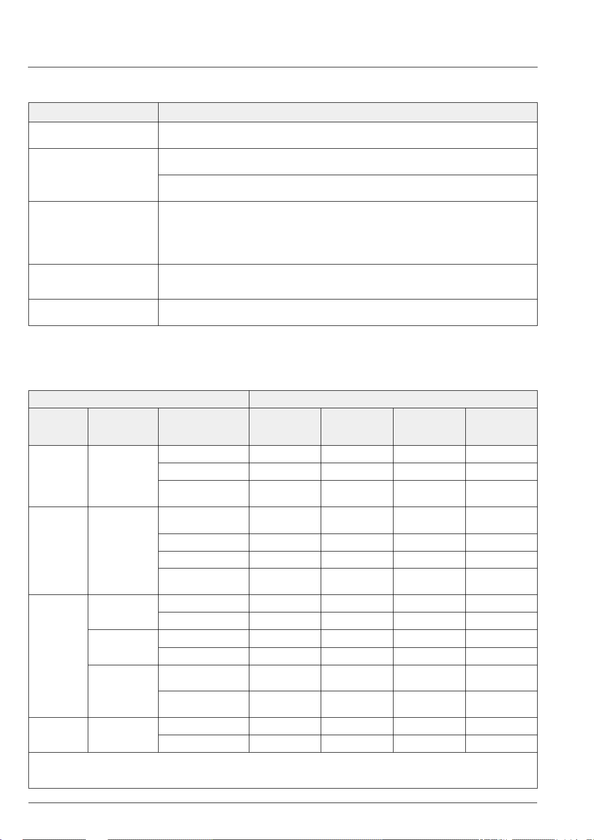
The MSP 34x1G family of single-chip Multistandard
Sound Processors cov ers the sound processin g of all
analog TV-Standards worldwide, as well as the NICAM
digital sound standards. The full TV sound processing,
starting with analog sound IF signal-in, down to processed analog AF-o ut, is performed on a single c hip.
Figure 1–1 shows a simplified functional block diagram
of the MSP 34x1G.
The MSP 34x1G has all functions of the MSP 34x0G
with the addition of a virtual surround sound feature.
Surround sound c an be r ep roduc ed to a c erta in ex ten t
with two loudspeak ers. The MSP 34x1G incl udes our
virtualizer algorithm “3D-PANORAMA” which has been
approved by the Dolby
1)
Laboratories for compl iance
with the "Virtual Dolby Surround" technology. In addition, the MSP 34x1G inc ludes our “PANORAMA” algorithm.
These TV sound proce ssing ICs include versions for
processing the multichannel television sound (MTS)
signal conforming to the standard recommended by
the Broadcast Television System s Committee (BTSC).
The DBX noise redu ct ion , or alter na tiv el y, MICRONAS
Noise Reduction (MNR) is performed alignment free.
Other processed standar ds are the Japanese FM-FM
multiplex standard (EIA-J) and the FM Stereo Radio
standard.
Current ICs have to p erform ad justment proc edures in
order to achieve good s ter eo sep arati on for BTS C and
EIA-J. The MSP 34x1G has optimum stereo performance without any adjustments.
All MSP 34x1G versions are pin and software downward-compatible to the MSP 34x0D. The MSP 34x1G
further simplifies controlling softw are. Standard sele ction requires a single I
2
C transmission only.
The MSP 34x1G ha s built-in automa tic functions: T he
IC is able to detect the actual sound standard automatically (Automatic Standard Detection). Furthermore,
pilot levels and identi fication signals can be ev aluated
internally with subsequent switching between mono/
stereo/bilingual; no I
2
C interaction is nece ssary (Auto-
matic Sound Selection).
The ICs are produced in submicron CMOS technology.
The MSP 34x1G is available in the following packages: PLCC68, PSDIP64, PSDIP52, PQFP80, and
PLQFP64.
Sound IF1
Sound IF2
I2S1
I2S2
SCART1
SCART2
SCART3
SCART4
MONO
ADC
SCART
DSP
Input
Select
De-
modulator
ADC
Pre-
processing
Prescale
Prescale
Fig. 1–1: Simplified functional block diagram of the MSP 34x1G
Source Select
Loud-
speaker
Sound
Processing
Headphone
Sound
Processing
DAC
DAC
DAC
DAC
SCART
Output
Select
Loudspeaker
Subwoofer
Headphone
I2S
SCART1
SCART2
6 MICRONAS INTERMETALL
Page 7
PRELIMINARY DATA SHEET MSP 34x1G
1.1. Features of the MSP 34x1G Family and Differences to MSP 34xxD
Feature (New features not available for MSP 34xxD are shaded gray.) 3401 3411 3421 3431 3441 3451
3D-PANORAMA virtualizer (approved by Dolby Laboratories) with noise generator
PANORAMA virtualizer algorithm
2
Standard Selection with single I
Automatic Standard Detection of terrestrial TV standards
Automatic Sound Selection (mono/stereo/bilingual), new registers MODUS, STATUS
Two selectable sound IF (SIF) inputs X X X X X X
Automatic Carrier Mute function X X X X X X
Interrupt output programmable (indicating status change)
Loudspeaker / Headphone channel with volume, balance, bass, treble, loudness X X X X X X
AVC: Automatic Volume Correction X X X X X X
Subwoofer output with programmable low-pass and complementary high-pass filter X X X X X X
5-band graphic equalizer for loudspeaker channel X X X X X X
Spatial effect for loudspeaker channel; processing of all deemphasis filtering X X X X X X
Four Stereo SCART (line) inputs, one Mono input; two Stereo SCART outputs X X X X X X
Complete SCART in/out switching matrix X X X X X X
2
S inputs; one I2S output XXXXXX
Two I
All analog FM-Stereo A2 and satellite standards; AM-SECAM L standard
C transmission X X X X X X
X X X X X X
X X X X X X
X X X X X X
X X X X X X
X X X X X X
X X X
Simultaneous demodulation of (very) high-deviation FM-Mono and NICAM
Adaptive deemphasis for satellite (Wegener-Panda, acc. to ASTRA specification) X X X
ASTRA Digital Radio (ADR) together with DRP 3510A X X X
All NICAM standards XX
Demodulation of the BTSC multiplex signal and the SAP channel
Alignment free digital DBX noise reduction for BTSC Stereo and SAP
Alignment free digital MICRONAS Noise Reduction (MNR) for BTSC Stereo and SAP
BTSC stereo separation (MSP 3421/41G also EIA-J) significantly better than spec.
SAP and stereo detection for BTSC system
Korean FM-Stereo A2 standard X X X X X
Alignment-free Japanese standard EIA-J
Demodulation of the FM-Radio multiplex signal
X X X
X X X X
X X X
X
X X X X
X X X X
X X X
X X X X
1.2. MSP 34x1G Version List
Version Status Descript ion
MSP 3401G planned FM Stereo (A2) Version
MSP 3411G planned NICAM and FM Stereo (A2) Version
MSP 3421G planned NTSC Version (A2 Korea, BTSC with MICRONAS Noise Reduction (MNR), and Japanese EIA-J system)
MSP 3431G planned BTSC Version
MSP 3441G planned NTSC Version (A2 Korea, BTSC with DBX noise reduction, and Japanese EIA-J system)
MSP 3451G available Global Version (all sound standards)
MICRONAS INTERMETALL 7
Page 8
MSP 34x1G PRELIMINARY DATA SHEET
1.3. MSP 34x1G Versions and their Application Fields
Table 1–1 provides an overview of TV sound standards that can be proce ssed by the MSP 34x1 G family. In addition , the MSP 34x1G is able to han dle the
terrestrial FM-Radio standa rd. Wi th the MSP 34x1G, a
complete multimedia receiver covering all TV sound
standards together with terrestrial and satellite radio
sound can be built; e ven ASTRA Di gital Radio can b e
processed (with a DRP 3510A coprocessor).
Table 1–1: TV Stereo Sound Standards covered by the MSP 34x1G IC Family (details see Appendix A)
MSP Ve rsion
3401
3401
3401
3411
TVSystem
B/G
L 6.5/ 5.85 AM-Mono/NICAM SECAM-L France
I 6.0/6.552 FM-Mono/NICAM PAL UK, Hong Kong
D/K
3451
Satellite
Position of Sound
Carrier /MHz
5.5/5.7421875 FM-Stereo (A2) PAL Germany
5.5/5.85 FM-Mono/NICAM PAL Scandinavia, Spain
6.5/6.2578125 FM-Stereo (A2, D/K1) SECAM-East Slovak. Rep.
6.5/6.7421875 FM-Stereo (A2, D/K2) PAL currently no broadcast
6.5/5.7421875 FM-Stereo (A2, D/K3) SECAM-East Poland
6.5/5.85 FM-Mono/NICAM (D/K, NICAM) PAL China, Hungary
6.5
7.02/7.2
7.38/7.56
etc.
Sound
Modulation
FM-Mono
FM-Stereo
ASTRA Digital Radio (ADR)
with DRP 3510A
Color
System
PAL
Broadcast e.g. in:
Europe Sat.
ASTRA
3421, 3441
3431
Tuner
4.5/4.724212 FM-Stereo (A2) NTSC Korea
M/N
FM-Radio 10.7 FM-Stereo Radio USA, Europe
SAW Filter
Composite
Video
4.5 FM-FM (EIA-J) NTSC Japan
4.5 BTSC-Stereo + SAP NTSC, PAL USA, Argentina
33 34 39 MHz 4.5 9 MHz
Sound
IF
Mixer
1
2
2
2
2
MSP 34x1G
2
SCART1
2
SCART2
Vision
Demodulator
SCART
Inputs
Mono
SCART1
SCART2
SCART3
SCART4
Loudspeaker
Subwoofer
Headphone
SCART
Outputs
I2S2ADRI2S1
Dolby
Pro Logic
Processor
DPL 351xA
ADR
Decoder
DRP 3510A
Fig. 1–2: Typical MSP 34x1G application
8 MICRONAS INTERMETALL
Page 9
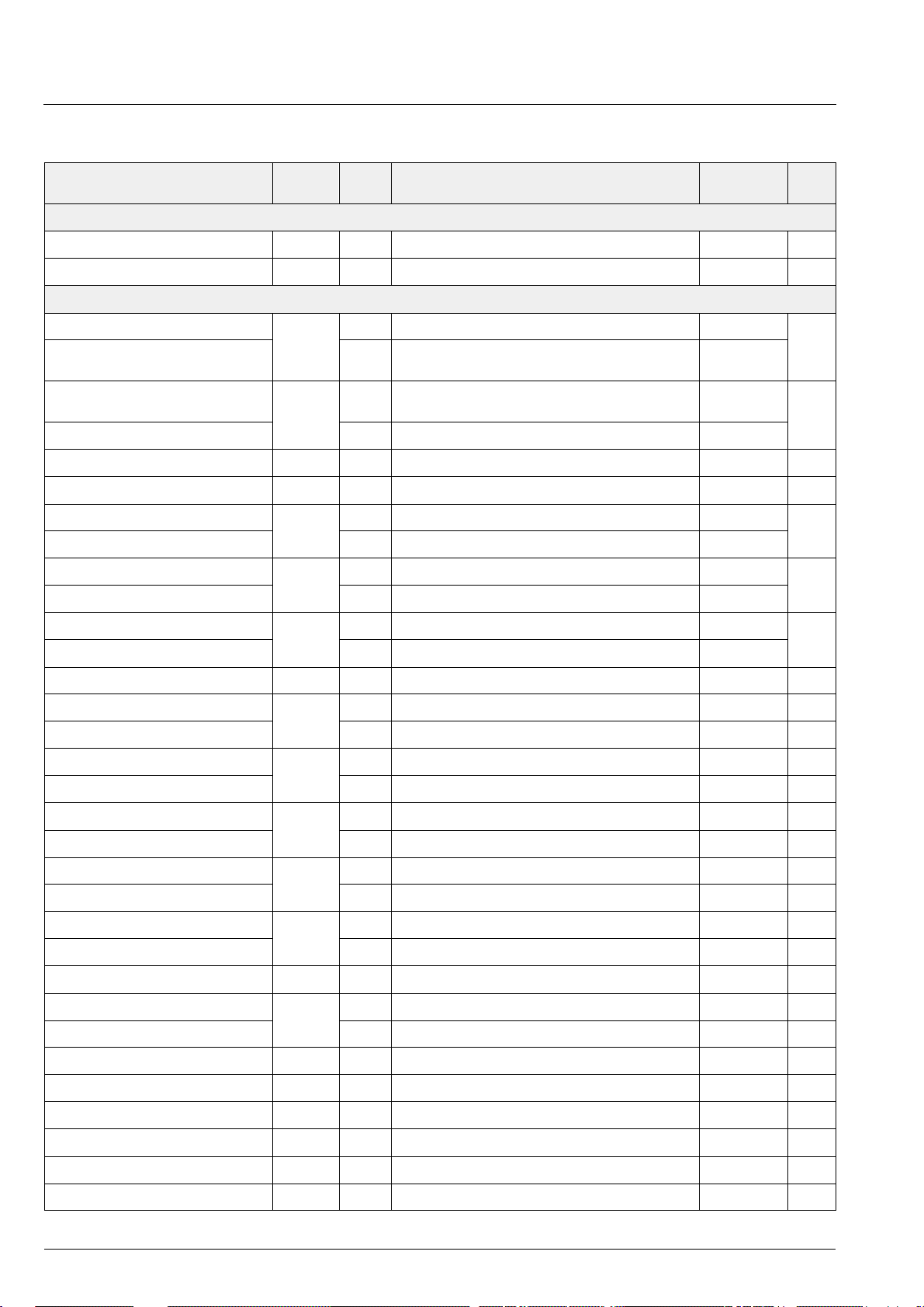
2. Functional Description
Automatic
MICRONAS INTERMETALL 9
ANA_IN1+
ANA_IN2+
AGC
A
D
DEMODULATOR
(incl. Carrier Mute)
Decoded
Standards:
NICAM
A2
AM
BTSC
EIA-J
SAT
FM-Radio
Deemphasis:
50/75 µs
DBX/MNR
Panda1
Deemphasis:
J17
Standard
and Sound
Detecti on
ADR-Bus Interface
Prescale
Prescale
FM/AM
NICAM
I2C Read-
Register
Sound Select
FM/AM
Stereo
or A/B
Stereo
or A
Stereo
or B
Loudspeaker
Channel
Head-
phone
Channel
Virtualizer
Noise
Generator
AVC
Bass/
Treble
or
Equal-
Bass/
Treble
Σ
Beeper
Loudness
LoudnessΣ
Complementary
Highpass
Lowpass
Spatial
Effects
Balance
Level
Adjust
Balance
Volume
Volume
D
D
A
DACM_SUB
A
DACM_L
DACM_R
DACA_L
DACA_R
PRELIMINARY DATA SHEET MSP 34x1G
I2S_DA_IN1
I2S_DA_IN2
SC1_IN_L
SC1_IN_R
SC2_IN_L
SC2_IN_R
SC3_IN_L
SC3_IN_R
SC4_IN_L
SC4_IN_R
MONO_IN
SCART DSP Input Select
I2S
Interface
I2S
Interface
A
I2S1
Prescale
I2S2
Prescale
SCART
D
Prescale
Source Select
I2S
Channel
Matrix
Quasi-
Peak
Channel
SCART1
Channel
Matrix
SCART2
Channel
Matrix
I2S
Interface
Quasi-Peak
Detector
Volume
Volume
I2C Read-
Register
D
A
D
A
SCART1_L/R
SCART2_L/R
SCART Output Select
I2S_DA_OUT
SC1_OUT_L
SC1_OUT_R
SC2_OUT_L
SC2_OUT_R
Fig. 2–1: Signal flow block diagram of the MSP 34x1G (input and output names correspond to pin names)
Page 10

MSP 34x1G PRELIMINARY DATA SHEET
2.1. Architecture of the MSP 34x1G Family
Fig. 2–1 on page 9 shows a simplified block diagram of
the IC. The block diagram con tains all features of the
MSP 3451G. Other m embers of the MSP 34x 1G family do not have the complete set of features: The
demodulator handles only a subset of the standards
presented in the demodulato r block; NICAM processing is only possible in the MSP 3411G and
MSP 3451G.
2.2. Sound IF Processing
2.2.1. Analog Sound IF Input
The input pins ANA_IN1+, ANA_IN2+, and ANA_IN
offer the possibility to connect two different sound IF
(SIF) sources to the MSP 34x1G. The analog-to-digital
conversion of the preselected sou nd IF signal is done
by an A/D-converter. An analog automatic gai n circuit
(AGC) allows a wide range of i nput levels. The highpass filters for med by the coupling capacito rs at pins
ANA_IN1+ and ANA_IN2+ see Section 8. “Appendix
E: Application Circuit” on page 100 are sufficient in
most cases to suppress video components. Some
combinations of SAW filter s and sound IF mixer ICs,
however, show large picture components on their outputs. In this case, further filtering is recommended.
BTSC-Mono + SAP: Detection and FM demodulation
of the aural carrier resulting in the MTS/MPX signal.
Detection and evaluation of the pilot carrier, detection
and FM demodulation of the SAP subcar rier. Processing of DBX noise reduction or MICRONAS Noise
Reduction (MNR).
Japan Stereo: Detection and FM demodulation of the
aural carrier resulting in the MPX signal. Demodulation
and evaluation of the identification signal and FM
demodulation of the (L−R)-carrier.
FM-Satellite Sound: Demodulation of one or two FM
carriers. Proces sing of high-dev iation mono or narrow
bandwidth mono, stereo, or bilingual satellite sound
according to the ASTRA specification.
−
FM-Stereo-Radio: Detection and FM demodulation of
the aural carri er res ultin g in th e MPX signal . Detec tion
and evaluation o f the pilot carrier and AM dem odulation of the (L−R)-carrier.
The demodulator blocks of all MSP 34x1G versions
have identical us er interfaces. Eve n completely different systems like the BTSC and NICAM systems are
controlled the same way. Standards are selected by
means of MSP Standar d Codes. Auto matic proc esses
handle standard detection and identification without
controller interaction. The key features of the
MSP 34x1G demodulator blocks are
2.2.2. Demodulator: Standards and Features
The MSP 34x1G is able to demodulate all TV-sound
standards worldwide including the digital N ICAM system. Depending on the MSP 34x1G version, the following demodulation modes can be performed:
A2 Systems: Detection and de modulatio n of two separate FM carriers (FM 1 and FM2), demodulation and
evaluation of the identification signal of carrier FM2.
NICAM Systems: Demodulation and decoding of the
NICAM carrier, detection and demodulation of the analog (FM or AM) carrier. For D/K-NICAM, the FM carrier
may have a maximum deviation of 384 kHz.
Very high deviation FM-Mono: Detection and robust
demodulation of one FM carrier with a maximum deviation of 540 kHz.
BTSC-Stereo: Detection and FM demodulation of the
aural carrier resulti ng in the MTS/MPX signal. Detection and evaluatio n of the pilot carri er, AM demodulation of the (L−R)-carrier and detection of the S AP subcarrier. Processing of DBX noise reduction or
MICRONAS Noise Reduction (MNR).
Standard Selection: The controlling of t he dem odulator is minimized: All parameters, such as tuning frequencies or filter bandwidth, are adjusted automatically by transmitting one single value to the
STANDARD SELECT regi ster. For all standards, specific MSP standard codes are defined.
Automatic Standard Detection: If the TV sound standard is unknown, the MSP 34x1G can automatically
detect the actual standard, switch to that standard, and
respond the actual MSP standard code.
Automatic Carrier Mute: To prevent noise e ffects or
FM identification problems in the absence of an FM
carrier, the MSP 34x1G offers a carrier mute feature,
which is activated a utomatically if the TV s ound standard is selected by means of the STANDARD SELECT
register. If no FM carrier is available at one of the two
MSP demodulator channels, the corresponding
demodulator output is muted.
10 MICRONAS INTERMETALL
Page 11
PRELIMINARY DATA SHEET MSP 34x1G
2.2.3. Preprocessing of Demodulator Signals
The NICAM signals must be processed by a deemphasis filter and adjusted in level. The analog demodulated signals mu st be processed by a deempha sis filter, adjusted in level, and dematrixed. The correct
deemphasis filter s are already selected by s etting the
standard in the STANDARD SELECT register. The
level adjustment ha s to be done by m eans of the FM/
AM and NICAM prescale registers. The necessary
dematrix function depends on the selected sound standard and the actual broadcasted sound m ode (mono,
stereo, or bilingual ). It can be manu ally set by the FM
Matrix Mode registe r or automatically set by the Automatic Sound Selection.
2.2.4. Automatic Sound Select
In the Automatic Sound Select mode, the dematrix
function is automatically selected based on the identification information in the STATUS register. No I
2
interaction is necess ary when the broadcasted sound
mode changes (e.g. from mono to stereo).
The demodulator supports the identification ch eck by
switching between mono compatible standards ( standards that have the same FM mon o carrier) automatically and non-audible. If B/G-FM or B/G-NICAM is
selected, the MSP will switch between these standards. The same action is performed for the standards: D/K1-FM, D/K2-FM, and D/K-NICAM. Switching
is only done in the abs ence of any stereo or bil ingual
identification. If identi fication is found, the MSP keeps
the detected standard.
In case of high bit-error rates, the MSP 34x1G automatically falls back fr om digital NICAM sound to analog FM or AM mono.
Table 2–1 summarizes all actions that take place when
Automatic Sound Select is switched on.
To provi de mo re flexibility, the Automatic Sound Select
block prepares four different source channels of
demodulated sound (Fig 2–3) . By cho osing on e of the
four demodulator ch annels, th e preferre d sound mo de
can be selected for eac h of the o utput c hanne ls (lo udspeaker, headphone, etc.). Thi s is done by means of
the Source Select registers.
The following source c hannels of demodulated sou nd
are defined:
– “FM/AM” channel: Analog mono sound, stereo if
available. In case of NICAM, analog mono only
(FM or AM mono).
– “Stereo or A/B” channel: Analog or digital mono
sound, stereo if available. In case of bilingual broadcast, it contains both languages A (left) and B
(right).
– “Stereo or A” channel: Analog or digital mono
sound, stereo if available. In case of bilingual broadcast, it contains language A (on left and right).
– “Stereo or B” channel: Analog or digital mono
sound, stereo if available. In case of bilingual broadcast, it contains language B (on left and right).
Fig 2–2 shows the s ource channel assignment of the
demodulated signal s in case of man ual mode. If man ual mode is required, more information can be found in
the section “D emodulator Sour ce Channels in M anual
Mode” on page 96. Fig 2–3 and Table 2–2 show the
source channel assignment of the demodulated signals in case of Au tomatic Sound Select mode for all
sound standards.
Note: The analog primary input channel contains the
signal of the mono FM/A M carrier or th e L+R signal of
the MPX carrier. The secondary input channel contains
the signal of t he 2nd FM carrier, the L−R signal of the
C
MPX carrier, or the SAP signal.
2.3. Preprocessing for SCART and
2
S Input Signals
I
2
The SCART and I
S inputs need only b e adjusted in
level by means of the SCART and I
2
S prescale regis -
ters.
Source Select
LS Ch.
Matrix
Output-Ch.
Matrices
must be set
according
the standard
SC2 Ch.
Matrix
primary
channel
secondary
channel
NICAM A
NICAM B
FM/AM
Prescale
NICAM
Prescale
FM-Matrix
FM/AM
NICAM
(Stereo or A/B)
0
1
Fig. 2–2: Source channel assignment of demodulated
signals in Manual Mode
Source Select
LS Ch.
Matrix
Output-Ch.
Matrices must
be set once to
stereo
SC2 Ch.
Matrix
primary
channel
secondary
channel
NICAM A
NICAM B
FM/AM
Prescale
NICAM
Prescale
Automatic
Sound
Select
FM/AM
Stereo or A/B
Stereo or A
Stereo or B
0
1
3
4
Fig. 2–3: Source channel assignment of demodulated
signals in Automatic Sound Select Mode
MICRONAS INTERMETALL 11
Page 12
MSP 34x1G PRELIMINARY DATA SHEET
Table 2–1: Performed actions of the Automatic Sound Selection
Selected TV Sound Standard Performed Actions
B/G-FM, D/K-FM, M-Korea,
and M-Japan
B/G-NICAM, L-NICAM, I-NICAM,
and D/K-NICAM
Evaluation of the identification signal and automatic switching to mono, stereo, or bilingual. Preparing four
demodulator source channels according to Table 2–2. Identification is acquired after 500 ms.
Evaluation of NICAM-C-bits and automatic switching to mono, stereo, or bilingual. Preparing four
demodulator source channels according to Table 2–2. NICAM detection is acquired within 150 ms.
In case of bad or no NICAM reception, the MSP switches automatically to FM/AM mono and switches
back to NICAM if possible. A hysteresis prevents periodical switching.
B/G-FM, B/G-NICAM
or
D/K1-FM, D/K2-FM, D/K3-FM,
and D/K-NICAM
Automatic searching for stereo/bilingual-identification in case of mono transmission. Automatic and nonaudible changes between Dual-FM and FM-NICAM standards while listening to the basic FM-Mono sound
carrier.
Example: If starting with B/G-FM-Stereo, there will be a periodical alternation to B/G-NICAM in the
absence of FM-Stereo/Bilingual or NICAM-identification. Once an identification is detected, the MSP
keeps the corresponding standard.
BTSC-STEREO, FM Radio Evaluation of the pilot signal and automatic switching to mono or stereo. Preparing four demodulator
source channels according to Table 2–2 . Detection of the SAP carrier. Pilot detection is acquired after
200 ms.
BTSC-SAP In the absence of SAP, the MSP switches to BTSC-Stereo if available. If SAP is detected, the MSP
switches automatically to SAP (see Table 2–2).
Table 2–2: Sound modes for the demodulator source channels with Automatic Sound Select
Source Channels in Automatic Sound Select Mode
Broadcasted
Sound
Standard
Selected
MSP Standard
3)
Code
Broadcasted
Sound Mode
FM/AM
(source select: 0)
Stereo or A/B
(source select: 1)
Stereo or A
(source select: 3)
Stereo or B
(source select: 4)
M-Korea
B/G-FM
D/K-FM
M-Japan
B/G-NICAM
L-NICAM
I-NICAM
D/K-NICAM
D/K-NICAM
(with high
deviation FM)
02
1)
03, 08
04, 05, 07, 0B
30
2)
08, 03
09
0A
2)
, 05
0B, 04
0C
MONO Mono Mono Mono Mono
1)
STEREO Stereo Stereo Stereo Stereo
BILINGUAL:
Languages A and B
NICAM not available or
Left = A
Right = B
Left = A
Right = B
AB
analog Mono analog Mono analog Mono analog Mono
error rate too high
2)
MONO analog Mono NICAM Mono NICAM Mono NICAM Mono
STEREO analog Mono NICAM Stereo NI CAM Stereo NICAM Stereo
BILINGUAL:
Languages A and B
analog Mono Left = NICAM A
Right = NICAM B
NICAM A NICAM B
20, 21 MONO Mono Mono Mono Mono
STEREO Stereo Stereo Stereo Stereo
20 MONO+SAP Mono Mono Mono Mono
BTSC
21 MONO+SAP Left = Mono
STEREO+SAP Stereo Stereo Stereo Stereo
Right = SAP
STEREO+SAP Left = Mono
Right = SAP
Left = Mono
Right = SAP
Left = Mono
Right = SAP
Mono SAP
Mono SAP
FM Radio 40 MONO Mono Mono Mono Mono
STEREO Stereo Stereo Stereo Stereo
1)
The Automatic Sound Select process will automatically switch to the mono compatible analog standard.
2)
The Automatic Sound Select process will automatically switch to the mono compatible digital standard.
3)
The MSP Standard Codes are defined in Table 3–7 on page 25.
12 MICRONAS INTERMETALL
Page 13

PRELIMINARY DATA SHEET MSP 34x1G
2.4. Source Selection and Output Channel Matrix
output level
The Source Selector makes it possible to distrib ute all
source signals ( one of the demodulator source channels, SCART, or I
2
S input) to the desired output chan-
nels (loudspeake r, headphone, etc.). All i nput and out-
[dBr]
12
−
put signals can be processed simultaneously. Each
source channel is identified by a unique source
18
−
address.
24
For each output channel, the sound mode can be set
−
to sound A, sound B , s tereo, or mono by mean s of t he
output channel matrix.
30−24−18−12
−
6
−
6
+
0
input level
If Automatic Sound Select is on, the output channel
[dBr]
matrix can stay fixed to stereo (transparent) for
demodulated signals.
Fig. 2–4: Simplified AVC characteristics
2.5. Audio Baseband Processing
2.5.1. Automatic Volume Correction (AVC)
Different sound sources (e.g . terres trial ch annel s, SAT
channels, or SCART) fairly often do not have the same
volume level. Advertisements during movies usually
have a higher volum e level than the movi e itself. This
results in annoying volume changes. The Automatic
Volume Correction (AVC) solves this problem by
equalizing the volume level.
To preven t clipping, the AVC’s gain decreases quickly
in dynamic boost conditions. To suppress oscillation
effects, the gain inc reases rather slowly for low leve l
inputs. The decay time is programma ble by means of
the AVC register (see page 34).
For input signals ranging from −24 dBr to 0 dBr, the
AVC maintains a fixed output level of −18 dBr. Fig. 2–4
shows the AVC output level versus its input le vel. For
prescale and volume registers set to 0 dB, a level of
0 dBr corresponds to full scale input/output. This is
– SCART input/output 0 dBr = 2.0 V
– Loudspeaker and Aux output 0 dBr = 1.4 V
rms
rms
2.5.2. Loudspeaker and Headphone Outputs
The following baseband features are implemented in
the loudspeaker and headphone output channels:
bass/treble, loudne ss, balance, and volum e. A square
wave beeper can be added to the loudspeaker and
headphone channel. The loudspeaker channel additionally performs: equalizer (not simultaneously with
bass/treble), spatial effects, and a subwoofer crossover filter.
2.5.3. Subwoofer Output
The subwoofer signa l is created by combin ing the left
and right channels d irectly behind the loudness block
using the formula (L+R)/2. Due to the division by 2, the
D/A converter will not be overloaded, even with full
scale input signal s. The subwo ofer sign al is filter ed by
a third-order low-pass with programmable corner frequency followed by a level adjustment. At the loudspeaker channels, a complementary high-pass filter
can be switched on. Subwoofe r and loudspeaker output use the same volum e (Loudspeaker Volume Register).
2.5.4. Quasi-Peak Detector
The quasi-peak reado ut register can be used to read
out the quasi-peak level of any i nput source. The feature is based on following filter time constants:
attack time: 1.3 ms
decay time: 37 ms
MICRONAS INTERMETALL 13
Page 14

MSP 34x1G PRELIMINARY DATA SHEET
2.6. Virtual Surround System Application Tips
2.6.1. Sweet Spot
Good results are only ob tained in a rather close area
along the middle axis between the two loudspeakers:
the sweet spot. Moving away from this position
degrades the effect.
2.6.2. Clipping
For the test at Do lby Labs, it is v ery impor tant to h ave
no clipping effects even with worst c ase signals. That
is, 2 Vrms input signal may no t clip. The SCART Input
Prescale register has to be set to values of 19
(25
) or lower (see SCART Input Prescale on page
dec
31).
Test signals: sine sweep with 2 V
L&R equal phase, L&R anti phase.
Listening tests: Do lby Trailers (train trailer, city trailer,
canyon trailer...)
; L only, R only,
RMS
hex
2.6.3. Loudspeaker Requirements
The loudspeakers used and their positioning inside the
TV set will greatly influence the performance of the virtualizer. The algorithm works with the direct sound
path. Reflected sound waves red uce th e effect. So it’s
most important to have as much direct sound as possible, compared to indire ct sound.
To obtain the approval for a TV set, Dolby Laboratories
require mounting the loud speakers in front of the set.
Loudspeakers ra diating to the side of the TV set will
not produce co nvincing effects. Good directio nality of
the loudspeakers towards the listener is optimal.
The virtualize r was special ly developed for implementation in TV sets. Even for rather small stereo TV's,
sufficient sound effects can be obtained. For small
sets, the loudspeaker pla cement s hould be to th e si de
of the CRT; for large screen sets (or 16:9 sets), mounting the loudspeakers below the CRT is acceptable
(large separation i s preferr ed, low freque ncy spea kers
should be outmost to avoid cancellation effects). Using
external loudspea ke rs wi th a la rg e s ter eo base wil l n ot
create optimal effects.
The loudspeakers shou ld be able to reprodu ce a wide
frequency range. The most impo rtant freque ncy rang e
starts from 160 Hz and ranges up to 5 kHz.
Great care has to be taken with s ystems that use one
common subwoofer: A single loudspeaker cannot
reproduce virtua l sound locations. The crossover frequency must be lower than 120 Hz.
2.6.4. Cabinet Requirements During listening tests at Dolby Laboratories, no reso-
nances in the cabinet should occur.
Good material to c heck for resonances are the Dolby
Trailers or other dynamic sound tracks.
14 MICRONAS INTERMETALL
Page 15

PRELIMINARY DATA SHEET MSP 34x1G
2
2.7. SCART Signal Routing
2.8. I
S Bus Interface
2.7.1. SCART DSP In and SCART Out Select
The SCART DSP Input Select and SCART Output
Select blocks include full matrix switching facilities. To
design a TV set with four pairs of SCART-inputs and
two pairs of SCART-outputs, no external switching
hardware is requir ed. The switches are controlled by
the ACB user register (see page 40).
2.7.2. Stand-by Mode
If the MSP 34x1G is switched off by first pulling
STANDBYQ low and then (after >1µs delay) switching
off the 5-V, but keeping the 8-V power supply (‘Stand-
by’-mode), the SCART switches maintain their position and function. This allows the copying from
selected SCART-inputs to SCART-outputs in the TV
set’s stand-by mode.
In case of power on o r starting from stand-by (switch-
ing on the 5-V supply, RESETQ going high 2 ms later),
all internal register s ex ce pt the A CB r egi st er (page 40)
are reset to the default configuration (see Table 3–5 on
page 22). The reset position of the ACB register
becomes active after the fi rst I
Baseband Processing part (subaddress 12
2
C transmis si on i nto the
). By
hex
transmitting the ACB register first, the reset stat e can
be redefined.
It is possible to route in an external coprocessor for
special effects, like surround processing and sound
field processing. Routi ng can be done with each in put
source and output chan nel via the I
2
S inputs and out-
puts.
Two possible interface formats are supported:
1. The SONY format: I2S_WS changes at the word
boundaries.
2. The PHILIPS format: I2S_WS changes one I2S_CL
period before the word boundaries.
2
S bus interface consists of five pins:
The I
1. I2S_DA_IN1, I2S_DA_IN2:
For input, four channels (two channels per line,
2*16 bits) per sampling cycle (32 kHz) are transmitted.
2. I2S_DA_OUT:
For output, two channels (2*16 bits) per sampling
cycle (32 kHz) are transmitted.
3. I2S_CL:
Gives the timing for the transmission of I
2
S serial
data (1.024 MHz).
4. I2S_WS:
The I2S_WS word strobe line defines the left and
right sample.
The MSP 34x1G normally serves as the master on the
2
S interface. In this case, the clock and word strobe
I
lines are driven by the MSP 34x1G. In slave mode,
these lines are input to the MSP 34x1G and the master
clock is synchronized to 576 times the I2S_WS rate
(32 kHz). NICAM operation is not possible in this
mode.
2
S options can be set by means of the MODUS
All I
register (see page 28).
2
A precise I
S timing diagram is shown in Fig. 4 –26 on
page 70.
MICRONAS INTERMETALL 15
Page 16

MSP 34x1G PRELIMINARY DATA SHEET
2.9. ADR Bus Interface
For the ASTRA Digital Radio System (ADR), the
MSP 3401G, MSP 3411G and MSP 3451G performs
preprocessing such as carrier selection and filtering.
Via the 3-line ADR-bus, the resulting signals are transferred to the DRP 3510A coprocessor, where the
source decoding i s performed. To be prepared for an
upgrade to ADR with an add iti on al DR P b oar d, t he fo llowing lines of MSP 34x1G should be provided on a
feature connector:
– AUD_CL_OUT
– I2S_DA_IN1 or I2S_DA_IN2
–I2S_DA_OUT
–I2S_WS
–I2S_CL
– ADR_CL, ADR_WS, ADR_DA
For more details, p lease refer to the DRP 3 510A dat a
sheet.
2.10.Digital Control I/O Pins and Status Change Indication
2.11. Clock PLL Oscillator and Crystal Specifications
The MSP 34x1G derives all internal system clocks
from the 18.432-MHz oscillator. In NICAM or in I
2
SSlave mode, the clock is phase-locked to the corresponding source. Therefore, it is not possible to use
NICAM and I
2
S-Slave mode at the same time.
For proper performance, the MSP clock oscillator
requires a 18.432-MHz crystal. Note that for the
phase-locked modes (NICAM, I
2
S-Slave), c r ys ta l s w it h
tighter tolerance are required.
Remark on using the crystal:
External capacit ors at each crystal pin to ground are
required. They are necess ary for tuning the open-loo p
frequency of the internal PLL and for stabilizing the frequency in closed-loop operation. The higher the
capacitors, the lower the resulting clock frequency.
The nominal free running frequency should match
18.432 MHz as closely as possible.
Clock measurements should be done at pin
AUD_CL_OUT. This pin must be activ ated for th is pu rpose (see Table 3–9 on page 28).
The static level of the digital input/output pins
D_CTR_I/O_0/1 is switchable between HIGH and
LOW via the I
(see page 40). This ena bles the contr olling of ex ternal
hardware switches or other devices via I
2
C-bus by means of the ACB register
2
C-bus.
The digital input/ou tput pins can b e set to high imp edance by means of the MODUS register (see page 28).
In this mode, the pins can be used as input. The current state can be read out of the STATUS register (see
page 29).
Optionally, the pin D_CTR_I/O_1 can be used as an
interrupt request sig nal to th e control ler, indicating any
changes in the read register STATUS. This makes polling unnecessary, I
2
C bus interactions are re duc ed to a
minimum (see STATUS register on page 29 and
MODUS register on page 28).
16 MICRONAS INTERMETALL
Page 17

PRELIMINARY DATA SHEET MSP 34x1G
3. Control Interface
2
C Bus Interface
3.1. I
3.1.1. Device and Subaddresses
2
The MSP 34x1G is controlled via the I
C bus slave
interface.
The IC is selected by transmitting one of the
MSP 34x1G device a ddresses. In order to allow up to
three MSP ICs to be connected to a single bus, an
address select pin (ADR_SEL) has been implemented.
With ADR_SEL pulled to high, low, or left open, the
MSP 34x1G respo nds to di fferent dev ic e a ddr ess es. A
device address pai r is defined as a write add ress (80,
84, or 88 hex) and a r ead address (81, 85, or 89 hex)
(see Table 3–1).
Writing is done by send ing the device write address,
followed by the suba ddress byte, two address bytes,
and two data bytes. Reading i s done by sending the
write device addre ss, fo llowed by the sub addres s byte
and two address byte s. Without se nding a stop con dition, reading of the addressed data is completed by
sending the devic e read address (81, 85, or 89 hex)
and reading two bytes of data. Refer to se ction 3.1.3.
for the I
Tips” on page 44 for proposals of MSP 34x1G I
2
C bus protoco l and to section “Pr ogramming
2
C telegrams. See Table 3–2 for a list of available subaddresses.
performed some o ther fu nctio n (for examp le, serv icing
an internal interru pt), it will hold the c lock line I2C_CL
LOW to force the transmitter into a wait state. The
positions within a transmission where this may happen
are indicated by ’ Wait’ in section 3.1.3. The m aximum
wait period of the MSP dur ing normal operation mo de
is less than 1 ms.
Internal hardware error handling:
In case of any internal hardware error (e.g. interruption
of the power supply of the MSP), the MSP’s wait
period is extended to 1.8 ms. After this time period
elapses, the MSP releases data and clo ck lines.
Indication and solving of the error status:
1. MSP 34x1G-versions until A1: To indicate the
error status, all further acknowledge bits will be left
high. The MSP can then b e reset by transmitting the
reset condition t o CONTROL while ignoring t he missing acknowledge bits.
2. MSP 34x1G-versions from A2 on: To i n di c a t e t h e
error status, the remaining acknowledge bits of the ac-
2
tual I
C-protocol will be left high. Additionally, bit[14] of
CONTROL is set to o ne. The MSP can then be reset
via the I
2
C bus by transmi tting the reset condition to
CONTROL.
Besides the possibility of hardware reset, the MSP can
also be reset by means of the RES ET bit in the CONTROL register by the controller via I
Due to the internal architecture of the MSP 34x1G, the
IC cannot react immediately to an I
2
C bus.
2
C request. The
typical response ti me is about 0. 3 ms. If the MSP cannot accept anothe r complete byte of data until it has
Indication of reset (only versions from A2 on):
Any reset, even caus ed by an unstable res et line etc.,
is indicated in bit[15] of CONTROL.
2
A general timing diagram of the I
C bus is shown in
Fig. 4–25 on page 68.
MICRONAS INTERMETALL 17
Page 18
MSP 34x1G PRELIMINARY DATA SHEET
Table 3–1: I
ADR_SEL Low High Left Open
Mode Write Read Write Read Write Read
MSP device address 80 hex 81 hex 84 hex 85 hex 88 hex 89 hex
2
C Bus Device Addresses
Table 3–2: I2C Bus Subaddresses
Name Binary Value Hex Value Mode Function
CONTROL 0000 0000 00 Read/Write Write: Software reset of MSP (see Table 3–3)
TEST 0000 0001 01 Write only for internal use
WR_DEM 0001 0000 10 Write write address demodulator
RD_DEM 0001 0001 11 Write read address demodulator
WR_DSP 0001 0010 12 Write write address DSP
RD_DSP 0001 0011 13 Write read address DSP
Read: Hardware error status of MSP
3.1.2. Description of CONTROL Register
Table 3–3: CONTROL as a Write Register
Name Subaddress Bit[15] (MSB) Bits[14:0]
CONTROL 00 hex 1 : RESET
0 : normal
0
Table 3–4: CONTROL as a Read Register (only MSP 34x1G-versions from A2 on)
Name Subaddress Bit[15] (MSB) Bit[14] Bits[13:0]
CONTROL 00 hex Reset st atus after last readi ng of CONTROL:
0 : no reset occured
1 : reset occured
Reading of CONTROL will reset the bits[15,14] of CONTROL. After Power-on,
read once to be resetted.
Internal hardware status:
0 : no error occured
1 : internal error occured
not of interest
bit[15] of CONTROL will be set; it must be
18 MICRONAS INTERMETALL
Page 19

PRELIMINARY DATA SHEET MSP 34x1G
3.1.3. Protocol Description
Write to DSP or Demodulator
Swrite
device
address
Wait
ACK sub-addr ACK addr-byte
high
ACK addr-byte
low
ACK data-byte-
high
ACK data-byte
low
ACK P
Read from DSP or Demodulator
Swrite
device
address
ACK sub-addr ACK addr-byte
Wait
high
ACK addr-byte
low
ACK S read
device
address
Wait
ACK dat a-byte-
high
Write to Control or Test Registers
Swrite
device
address
Wait
Note: S = I
P = I
ACK sub-addr ACK data-byte
2
C-Bus Start Condition from master
2
C-Bus Stop Condition from master
high
ACK data-byte
low
ACK P
ACK = Acknowledge-Bit: LOW on I2C_DA from slave (= MSP, light gray)
or master (= controller dark gray)
NAK = Not Acknowledge-Bit: HIGH on I2C_DA from master (dark gray) to indicate ‘End of Read’
or from MSP indicating internal error state
2
Wait = I
C-Clock line is held low, while the MSP is processing the I2C command. This waiting time is
max. 1 ms
ACK data-byte
low
NAK P
I2C_DA
1
0
S P
I2C_CL
2
Fig. 3–1: I
C bus protocol (MSB first; data must be stable while clock is high)
MICRONAS INTERMETALL 19
Page 20

MSP 34x1G PRELIMINARY DATA SHEET
3.1.4. Proposals for General MSP 34x1G I2C Telegrams
3.1.4.1. Symbols
, 84
daw write device address (80
dar read device address (81
hex
hex
, 85
hex
hex
or 88
or 89
< Start Condition
> Stop Condition
aa Address Byte
dd Data Byte
3.1.4.2. Write Telegrams
<daw 00 d0 00> write to CONTROL register
<daw 10 aa aa dd dd> write data into demodulator
<daw 12 aa aa dd dd> write data into DSP
3.1.4.3. Read Telegrams
hex
hex
)
)
<daw 11 aa aa <dar dd dd> read data from demodulator
<daw 13 aa aa <dar dd dd> read data from DSP
3.1.4.4. Examples
<80 00 80 00> RESET MSP statically
<80 00 00 00> Clear RESET
<80 10 00 20 00 03> S et dem odulator to stand. 03
hex
<80 11 02 00 <81 dd dd> Read STATUS
<80 12 00 08 01 20> Set loudspeaker channel source to NICAM and Matrix to STEREO
More examples of typical application protocols are listed in section “Programming Tips” on page 44.
20 MICRONAS INTERMETALL
Page 21

PRELIMINARY DATA SHEET MSP 34x1G
3.2. Start-Up Sequence:
Power-Up and I
2
C Controlling
After POWER ON or RESET (see Fig . 4–24) , the IC is
in an inactive state. All registers are in the reset position (see tables 3–5 a nd 3–6), the analog outp uts are
muted. The controller has to initialize all registers for
which a non-default setting is necessary.
3.3. MSP 34x1G Programming Interface
3.3.1. User Registers Overview
The MSP 34x1G is controll ed by means o f user registers. The compl ete list of all user registers is give n in
the following tables. T he registers are partitioned in to
the Demodulator section (Subaddress 10
ing, 11
sections (Subad dres s 12
for reading) and the Baseband Processing
hex
for writing, 13
hex
for writ-
hex
for read-
hex
ing).
Write and read register s are 16-bit wide, whereby the
MSB is denoted bit [15]. Transmissions via I
2
C bus
have to take place in 16-bit words (two byte transfers, with
the most significant byte tran sferred first). All write reg isters, except the demodulator write registers, are readable.
Unused parts of the 16-bit writ e registers must be zero.
Addresses not given in this table must not be written.
For reasons of software compatibility to the
MSP 34x0D, an Manual/Compatibility Mode is available. More read and write registers together with a
detailed descrip tion of this mode can be found i n the
“Appendix B: Manual/Compatibility Mode” on page 83.
An overview of all MSP 34x1G Write Registers is
shown in Table 3–5; all Read Registers are given in
Table 3–6.
MICRONAS INTERMETALL 21
Page 22
MSP 34x1G PRELIMINARY DATA SHEET
Table 3–5: List of MSP 34x1G Write Registers
Write Register Address
(hex)
I2C Subaddress = 10
; Registers are
hex
not
Bits Description and Adjustable Range Reset See
Page
readable
STANDARD SELECT 00 20 [15..0] Initial Programming of complete Demodulator 00 00 26
2
MODUS 00 30 [15..0] Demodulator, Automatic and I
I2C Subaddress = 12
; Registers are
hex
all
readable by using I2C Subaddress = 13
hex
S options 00 00 28
Volume loudspeaker channel 00 00 [15..8] [+12 dB ... −114 dB, MUTE] MUT E 33
Volume / Mode loudspeaker channel [7..0] 1/8 dB Steps,
Reduce Volume / Tone Control / Compromise
Balance loudspeaker channel [L/R] 00 01 [15..8] [0...100 / 100% and 100 / 0...100%]
00
hex
100%/100% 34
[−127...0 / 0 and 0 / −127...0 dB]
Balance mode loudspeaker [7..0] [Linear mode / logarithmic mode] linear mode
Bass loudspeaker channel 00 02 [15..8] [+20 dB ... −12 dB] 0 dB 35
Treble loudspeaker channel 00 03 [15..8] [+15 dB ... −12 dB] 0 dB 36
Loudness loudspeaker channel 00 04 [15..8] [0 dB ... +17 dB] 0 dB 37
Loudness filter characteristic [7..0] [NO RMA L, SUP ER_B AS S] NORMA L
Spatial effect strength loudspeaker ch. 00 05 [15..8] [−100%...OFF...+100%] OFF 38
Spatial effect mode/customize [7..0] [SBE, SBE+PSE] SBE+PSE
Volume headphone channel 00 06 [15..8] [+12 dB ... −114 dB, MUTE] MUT E 33
Volume / Mode headphone channel [7..0] 1/8 dB Steps, Reduce Volume / Tone Control 00
hex
Volume SCART1 output channel 00 07 [15..8] [+12 dB ... −114 dB, MUTE] MUT E 39
2
Loudspeaker source select 00 08 [15..8] [FM/AM, NICAM, SCART, I
S1, I2S2] FM/AM 32
Loudspeaker channel matrix [7..0] [SOUNDA, SOUNDB, STEREO, MONO...] SOUNDA 32
2
Headphone source select 00 09 [15..8] [FM/AM, NICAM, SCART, I
S1, I2S2] FM/AM 32
Headphone channel matrix [7..0] [SOUNDA, SOUNDB, STEREO, MONO...] SOUNDA 32
2
SCART1 source select 00 0A [15..8] [FM/AM, NICAM, SCART, I
S1, I2S2] FM/AM 32
SCART1 channel matrix [7..0] [SOUNDA, SOUNDB, STEREO, MONO...] SOUNDA 32
2
S source select 00 0B [15..8] [FM/AM, NICAM, SCART, I2S1, I2S2] FM/AM 32
I
2
S channel matrix [7..0] [SOUNDA, SOUNDB, STEREO, MONO...] SOUNDA 32
I
2
Quasi-peak detector source select 00 0C [15..8] [FM/AM, NICAM, SCART, I
S1, I2S2] FM/AM 32
Quasi-peak detector matrix [7..0] [SOUNDA, SOUNDB, STEREO, MONO...] SOUNDA 32
Prescale SCART input 00 0D [15..8] [00
Prescale FM/AM 00 0E [15..8] [00
hex
hex
... 7F
... 7F
]00
hex
]00
hex
hex
hex
31
30
FM matrix [7..0] [NO_MAT, GSTEREO, KSTEREO] NO_MAT 31
Prescale NICAM 00 10 [15..8] [00
2
Prescale I
S2 00 12 [15..8] [00
hex
hex
... 7F
... 7F
ACB : SCART Switches a. D_CTR_I/O 00 13 [15..0] Bits [15..0] 00
Beeper 00 14 [15..0] [00
2
Prescale I
S1 00 16 [15..8] [00
hex
hex
... 7F
... 7F
] (MSP 3411G, MSP 3451G only) 00
hex
]10
hex
]/[00
hex
hex
... 7F
hex
]10
] 00/00
hex
hex
hex
hex
hex
hex
31
31
40
40
31
Mode tone control 00 20 [15..8] [BASS/TREBLE, EQUALIZER] BASS/TREB 35
22 MICRONAS INTERMETALL
Page 23
PRELIMINARY DATA SHEET MSP 34x1G
T able 3–5: List of MSP 34x1G Write Registers, continued
Write Register Address
(hex)
Bits Description and Adju s table Range Reset See
Page
Equalizer loudspeaker ch. band 1 00 21 [15..8] [+12 dB ... −12 dB] 0 dB 36
Equalizer loudspeaker ch. band 2 00 22 [15..8] [+12 dB ... −12 dB] 0 dB 36
Equalizer loudspeaker ch. band 3 00 23 [15..8] [+12 dB ... −12 dB] 0 dB 36
Equalizer loudspeaker ch. band 4 00 24 [15..8] [+12 dB ... −12 dB] 0 dB 36
Equalizer loudspeaker ch. band 5 00 25 [15..8] [+12 dB ... −12 dB] 0 dB 36
Automatic Volume Correction 00 29 [15..8] [ off, on, decay time] off 34
Subwoofer level adjust 00 2C [15..8] [0 dB ... −30 dB, mute] 0 dB 39
Subwoofer corner frequency 00 2D [15..8] [50 Hz ... 400 Hz] 00
hex
39
Subwoofer complementary high-pass [7..0] [off, on] off 39
Balance headphone channel [L/R] 00 30 [15..8] [0...100 / 100% and 100 / 0...100%]
100 %/100 % 34
[−127...0 / 0 and 0 / −127...0 dB]
Balance mode headphone [7..0] [Linear mode / logarithmic mode] linear mode
Bass headphone channel 00 31 [15..8] [+20 dB ... −12 dB] 0 dB 35
Treble headphone channel 00 32 [15..8] [+15 dB ... −12 dB] 0 dB 36
Loudness headphone channel 00 33 [15..8] [0 dB ... +17 dB] 0 dB 37
Loudness filter characteristic [7..0] [NORMA L, SUPER_B AS S] N ORMAL
Volume SCART2 output channel 00 40 [15..8] [+12 dB ... −114 dB, MUT E] 00
2
SCART2 source select 00 41 [15..8] [FM, NICAM, SCART, I
S1, I2S2] FM 32
hex
39
SCART2 channel matrix [7..0] [SOUNDA, SOUNDB, STEREO, MONO...] SOUNDA 32
Virtual Surround OFF/ON switch 00 48 [15..8] [OFF/ON] 00
Virtual Surround spatial effect strength 00 49 [15..8] [0% - 100%] 00
Virtual Surround 3D effect strength 00 4A [15..8] [0% - 100%] 00
Virtual Surround mode 00 4B [15..0] [PANORAMA/3D-PANORAMA] 00
Noise generator 00 4D [15..0] [OFF/ON, Noise_L, Noise_C, Noise_R, Noise_S] 00
hex
hex
hex
hex
hex
41
41
41
41
42
MICRONAS INTERMETALL 23
Page 24
MSP 34x1G PRELIMINARY DATA SHEET
Table 3–6: List of MSP 34x1G Read Registers
Read Register Address
(hex)
I2C Subaddress = 11
; Registers are
hex
not
Bits Description and Adjustable Range See
Page
writable
STANDARD RESULT 00 7E [15..0] Result of Automatic Standard Detection (see Table 3–8) 29
STATUS 02 00 [15..0] Monitoring of internal settings e.g. Stereo, Mono, Mute etc. . 29
I2C Subaddress = 13
Quasi peak readout left 00 19 [15..0] [00
Quasi peak readout right 00 1A [15..0] [00
MSP hardware version code 00 1E [15..8] [00
MSP major revision code [7..0] [00
MSP product code 00 1F [15..8] [00
MSP ROM version code [7..0] [00
; Registers are
hex
not
writable
hex
hex
hex
hex
hex
hex
... 7FFF
... 7FFF
... FF
... FF
... FF
... FF
]16 bit two’s complement 43
hex
]16 bit two’s complement 43
hex
]43
hex
]43
hex
]43
hex
]43
hex
24 MICRONAS INTERMETALL
Page 25
PRELIMINARY DATA SHEET MSP 34x1G
3.3.2. Description of User Registers
T able 3–7: Standard Codes for STANDARD SELECT register
MSP Standard Code
(Data in hex)
TV Sound Standard Sound Carrier
Frequencies in MHz
MSP 34x1G Version
Automatic Standard Detection
00 01 Start Automatic Standard Detection all
Standard Selection
00 02 M-Dual FM-Stereo 4.5/4.724212 3401, -11, -21, -41, -51
00 03 B/G -Dual FM-Stereo
00 04 D/K1-Dual FM-Stereo
00 05 D/K2-Dual FM-Stereo
1)
2)
2)
00 06 D/K -FM-Mono with HDEV3
Standard Detection,
3)
HDEV3
SAT-Mono (i.e. Eutelsat, s. Table 6–17)
3)
, not detectable by Automatic
5.5/5.7421875 3401, -11, -51
6.5/6.2578125
6.5/6.7421875
6.5
00 07 D/K3-Dual FM-Stereo 6.5/5.7421875
00 08 B/G -NICAM-FM
1)
5.5/5.85 3411, -51
00 09 L -NICAM-AM 6.5/5.85
00 0A I -NICAM-FM 6.0/6.552
00 0B D/K -NICAM-FM
2)
00 0C D/K -NICAM-FM with HDEV2
4)
, not detectable by Automatic
6.5/5.85
6.5/5.85
Standard Detection, for China
00 0D D/K -NICAM-FM with HDEV3
, not detectable by Automatic
6.5/5.85
3)
Standard Detection, for China
00 20 BTSC-Stereo 4.5 3421, -31, -41, -51
00 21 BTSC-Mono + SAP
00 30 M-EIA-J Japan Stereo 4.5 3421, -41, -51
00 40 FM-Stereo Radio 10.7 3421, -31, -41, -51
00 50 SAT-Mono (s. Table 6–17) 6.5 3401, -11, -51
00 51 SAT-Stereo (s. Table 6–17) 7.02/7.20
00 60 SAT ADR (Astra Digital Radio) 7.2
1)
In case of Automatic Sound Select, the B/G-codes 3
2)
In case of Automatic Sound Select, the D/K-codes 4
3)
HDEV3: Max. FM deviation must not exceed 540 kHz
4)
HDEV2: Max. FM deviation must not exceed 360 kHz
hex
hex
and 8
, 5
hex
are equivalent.
hex
and B
are equivalent.
hex
MICRONAS INTERMETALL 25
Page 26

MSP 34x1G PRELIMINARY DATA SHEET
3.3.2.1. STANDARD SELECT Register
The TV sound sta ndard of t he MS P 3 4x1G d emodul ator is determined by the STANDARD SELECT register.
There are two ways to use the S TANDARD SELE CT
register:
– Setting up the demodulator for a TV sound standard
by sending the corresponding standard code with a
single I
– Starting the Automatic Standard Detection for ter-
restrial TV standa rds. This is the most comfortable
way to set up the demodulator. Within 0.5 s, the
detection and set-up of the actual TV sound standard is performed. The detected standard can be
read out of the STANDARD RESULT regi s ter by th e
control processor. This feature is recommended for
the primary set-up of a TV set. Outputs should be
muted during Automatic Standard Detection.
The Standard Codes are listed in Table 3–7.
Selecting a TV sound standard via the STANDARD
SELECT register initializes the demodulator. This
includes: AGC, tuning frequency, band-pass filters,
demodulation mode (FM, AM, or NICAM), carrier
mute, deemphasis, and identification mode.
2
C-Bus transmission.
3.3.2.2. Refresh of STANDARD SELECT Register
A general refresh of the STA NDAR D S EL ECT r eg ister
is not allowed. However, the following method
enables watching the MSP 34x1G “alive” status and
detection of accidental resets (only versions A2 and
later):
– After Power-on, bit[15] of CONTROL will be set; it
must be read once to enable the reset-detection
feature.
– Reading of the CONTROL register and checking
the reset indicator bit[15] .
– If bit[15] is “0”, any refresh of the STANDARD
SELECT register is not allowed.
– If bit[15] is “1”, indicating a reset, a refresh of the
STANDARD SELECT register and all other MSPG
registers is necessary.
If a present sound standard is im poss ibl e for a spe ci fic
MSP version, it s witches t o the analo g mono sou nd of
this standard. In that c ase stereo or bilingual pr ocessing will not be possible.
For a complete setup of the TV sound processing from
analog IF input t o the source selection, the trans missions as shown in Section 3.5. are necessary.
Note: The FM matrix is set automatically if Automatic
Sound Select is active (MODUS[0]=1). In this case, the
FM matrix will be ini ti ali ze d wi th “ Sound A Mono”. During operation, the FM matrix will be automatically
selected accordin g to the actual id entification information.
For reasons of software compatibility to the
MSP 34x0D, a Manual/Compatibility mode is available. A detailed de scription of this mo de can be found
on page 83.
26 MICRONAS INTERMETALL
Page 27
PRELIMINARY DATA SHEET MSP 34x1G
3.3.2.3. STANDARD RESULT Register
If Automatic Standard Detection is selected in the
STANDARD SELECT reg ister, status and result of t he
Automatic Standard Detection process can be read out
of the STANDARD RESULT register. The possible
results are based on the mentioned Standard Code
and are listed in Table 3–8.
In cases where no s ound st andard h as been detected
(no standard present, t oo much noise, st rong interferers, etc.) the STANDARD RESULT register contains
00 00
. In that case, the controller has to start further
hex
actions (for example, set the standard according to a
preference list or by manual input).
As long as the STANDARD RESULT register contains
a value greater than 07 FF
, the Automatic Standard
hex
Detection is still active. During this period, the MODUS
and STANDARD SELECT register must not be written.
The STATUS register will be updated when the Automatic Standard Detection has finished.
If a present sound standard is impossible for a specific
MSP version, it detects and switches to the analog
mono sound of this standard.
Example:
The MSPs 3431G and 3441G will detect a B/G-NICAM
signal as standard 3 and w ill switch to the ana log FMMono sound.
T able 3–8: Results of the Automatic Standard
Detection
Broadcasted Sound
Standard
Automatic Standard
Detection could not
find a sound standard
B/G-FM 0003
B/G-NICAM 0008
I 000A
FM-Radio 0040
M-Korea
M-Japan
M-BTSC
L-AM
D/K1
D/K2
L-NICAM
D/K-NICAM
Automatic Standard
Detection st ill active
STANDARD RESULT Register
Read 007E
0000
0002
0020
0030
0009
0004
0009
000B
>07FF
hex
hex
hex
hex
hex
hex
(if MODUS[14,13]=00)
hex
(if MODUS[14,13]=01)
hex
(if MODUS[14,13]=10)
hex
(if MODUS[12]=0)
hex
(if MODUS[12]=1)
hex
(if MODUS[12]=0)
hex
(if MODUS[12]=1)
hex
hex
MICRONAS INTERMETALL 27
Page 28

MSP 34x1G PRELIMINARY DATA SHEET
3.3.2.4. Write Registers on I2C Subaddress 10
Table 3–9: Write Registers on I2C Subaddress 10
Register
Function Name
Address
STANDARD SELECTION
00 20
hex
STANDARD SELECTION Register
Defines TV Sound or FM-Radio Standard
bit [15:0] 00 01
00 02
...
00 60
start Automatic Standard Detection
hex
Standard Codes (see Table 3–7))
hex
hex
MODUS
00 30
hex
MODUS Register
General MSP 34x1G Options
bit [0] 0/1 off/on: Automatic Sound Select
bit [1] 0/1 disable/enable STATUS change indication by means of
the digital I/O pin D_CTR_I/O_1
Necessary condition: MODUS[3] = 0 (active)
hex
hex
STANDARD_SEL
MODUS
bit [2] 0 undefined, must be 0
bit [3] state of digital output pins D_CTR_I/O_0 and _1
0 active: D_CTR_I/O_0 and _1 are output pins
(can be set by means of the ACB register.
see also: MODUS[1])
1 tristate: D_CTR_I/O_0 and _1 are input pins
(level can be read out of STATUS[4,3])
2
bit [4] 0/1 active/tristate state of I
bit [5] 0/1 master/slave mode of I
S output pins
2
S interface (must be set to 0
(= Master) in case of NICAM mode)
2
bit [6] 0/1 Sony/Philips format of I
S word strobe
bit [7] 0/1 active/tristate state of audio clock output pin
AUD_CL_OUT
bit [8] 0/1 ANA_IN_1+/ANA_IN_2+;
select analog sound IF input pin
bit [11:9] 0 undefined, must be 0
Preference in Automatic Standard Detection:
bit [12] detected 6.5 MHz carrier is interpreted as:
1)
0 standard L (SECAM)
1 standard D/K1, D/K2 or D/K NICAM
bit [14:13] detected 4.5 MHz carrier is interpreted as:
1)
0 standard M (Korea)
1 standard M (BTSC)
2 standard M (Japan)
3 carrier at 4.5 MHz is ignored (chroma carrier)
bit [15] 0 undefined, must be 0
1)
Valid at the next start of Automatic Standard Detection.
28 MICRONAS INTERMETALL
Page 29

PRELIMINARY DATA SHEET MSP 34x1G
3.3.2.5. Read Registers on I2C Subaddress 11
hex
T able 3–10: Read Registers on I2C Subaddress 11
Register
Function Name
Address
STANDARD RESULT
00 7E
hex
STANDARD RESULT Register
Readback of the detected TV Sound or FM-Radio Standard
bit [15:0] 00 00
Automatic Standard Detection could not find
hex
a sound standard
00 02
MSP Standard Codes (see Table 3–8)
hex
...
00 40
>07 FF
hex
Automatic Standard Detection still active
hex
STATUS
02 00
hex
STATUS Register
Contains all user relevant internal information about the status of the MSP
hex
STANDARD_RES
STATUS
bit [0] undefined
bit [1] 0 detected primary carrier (Mono or MPX carrier)
1 no primary carrier detected
bit [2] 0 detected secondary carrier (2nd A2 or SAP carrier)
1 no secondary carrier detected
bit [3] 0/1 low/high level of digital I/O pin D_CTR_I/O_0
bit [4] 0/1 low/high level of digital I/O pin D_CTR_I/O_1
bit [5,9] 00 analog sound standard (FM or AM) active
01 not obtainable
10 digital sound (NICAM) available (MSP 3411G and
MSP 3451G only)
11 bad reception condit io n of di gi ta l so un d (N ICAM ) due to :
a. high error rate
b. unimplemented sound code
c. data transmissio n o nly
bit [6] 0/1 mono/stereo indication
bit [7] 0/1 “1” indicates independent mono sound
(only for NICAM on MSP 3411G and MSP 3451G)
bit [8] 0/1 “1” indicates bilingual sound mode or SAP present
bit [15:10] undefined
If STATUS change indication is activated by means of MODUS[1]: Each
change in the STATUS register sets the digital I/O pin D_CTR_I/O_1 to high
level. Reading the STATUS register resets D_CTR_I/O_1.
MICRONAS INTERMETALL 29
Page 30

MSP 34x1G PRELIMINARY DATA SHEET
3.3.2.6. Write Registers on I2C Subaddress 12
hex
Table 3–11: Write Registers on I2C Subaddress 12
Register
Function Name
Address
PREPROCESSING
00 0E
hex
FM/AM Prescale
bit [15:8] 00
hex
Defines the input prescale gain for the demodulated
... FM or AM signal
7F
hex
00
hex
off (RESET condition)
For all FM modes except satellite FM and AM-mode, the combinations of prescale value and FM deviation listed below lead to internal full scale.
FM mode
bit [15:8] 7F
48
30
24
18
13
hex
hex
hex
hex
hex
hex
28 kHz FM deviation
50 kHz FM deviation
75 kHz FM deviation
100 kHz FM deviation
150 kHz FM deviation
180 kHz FM deviation (limit)
hex
PRE_FM
FM high deviation mode (HDEV2, MSP Standard Code = C
bit [15:8] 30
14
hex
hex
150 kHz FM deviation
360 kHz FM deviation (limit)
hex
)
FM very high deviation mode (HDEV3, MSP Standard Code = 6 and D
bit [15:8] 20
1A
hex
hex
450 kHz FM deviation
540 kHz FM deviation (limit)
Satellite FM with adaptive deemphasis
bit [15:8] 10
hex
recommendation
AM mode (MSP Standard Code = 9)
bit [15:8] 7C
hex
recommendation for SIF input levels from
0.1 V
to 0.8 V
pp
pp
(Due to the AGC being switched on, the AM-output level
remains stable and independent of the actual SIF-level in
the mentioned input range)
hex
)
30 MICRONAS INTERMETALL
Page 31

PRELIMINARY DATA SHEET MSP 34x1G
T able 3–11: Write Registers on I
Register
Function Name
Address
(continued)
00 0E
hex
FM Matrix Modes
Defines the dematrix function for the demodulated FM signal
bit [7:0] 00
01
02
03
04
hex
hex
hex
hex
hex
In case of Automatic S ound Select, the FM Matrix Mod e is set automatically,
i.e. the low-part of any I
To enab le a For ced Mono Mode for al l analo g ster eo syst ems by o verridi ng the
internal pilot or identification evaluation, the following steps must be transmitted:
1. MODUS with bit[0] = 0 (Automatic Sound Select off)
2. FM Presc./Matrix with FM Matrix = Sound A Mono (SAP: Sound B Mono)
3. Select FM/AM source channel, with channel matrix set to “Stereo” (transparent)
2
C Subaddress 12
, continued
hex
no matrix (used for bilingual and unmatrixed stereo sound)
German stereo (Standard B/G)
Korean stereo (also used for BTSC, EIA-J and FM Radio)
sound A mono (left and right channel contain the mono
sound of the FM/AM mono carrier)
sound B mono
2
C transmission to the register 00 0E
is ignored.
hex
FM_MA TRIX
00 10
00 16
00 12
00 0D
hex
hex
hex
hex
NICAM Prescale
Defines the input prescale value for the digital NICAM signal
bit [15:8] 00
hex
... 7F
prescale gain
hex
examples:
00
20
5A
7F
hex
hex
hex
hex
off
0dB gain
9 dB gain (recommendation)
12 dB gain (maximum gain)
+
I2S1 Prescale
I2S2 Prescale
2
Defines the input prescale value for digital I
bit [15:8] 00
hex
... 7F
prescale gain
hex
S input signals
examples:
00
10
7F
hex
hex
hex
off
0 dB gain (recommendation)
18 dB gain (maximum gain)
+
SCART Input Prescale
Defines the input prescale value for the analog SCART input signal
PRE_NICAM
PRE_I2S1
PRE_I2S2
PRE_SCART
bit [15:8] 00
hex
... 7F
prescale gain
hex
examples:
00
19
hex
hex
off
0dB gain (2 V
input leads to digital full scale)
RMS
Due to the Dolby requirements, this is the maximum
input signal.
RMS
7F
hex
value allowed to prohibit clipping of a 2 V
14 dB gain (400 mV
+
input leads to digital full scale)
RMS
MICRONAS INTERMETALL 31
Page 32

MSP 34x1G PRELIMINARY DATA SHEET
Table 3–11: Write Registers on I
Register
Function Name
2
C Subaddress 12
hex
Address
SOURCE SELECT AND OUTPUT CHANNEL MATRIX
Source for:
00 08
00 09
00 0A
00 41
00 0B
00 0C
hex
hex
hex
hex
hex
hex
Loudspeaker Output
Headphone Output
SCART1 DA Output
SCART2 DA Output
2
S Output
I
Quasi-Peak Detector
bit [15:8] 0 “FM/AM”: demodulated FM or AM mono signal
1 “Stereo or A/B”: demodulator Stereo or A/B signal
(in manual mode, this source is identical to the NICAM
source in the MSP 3410D)
3 “Stereo or A”: demodulator Stereo Sound or
Language A (only defined for Automatic Sound Select)
4 “Stereo or B”: demodulator Stereo Sound or
Language B (only defined for Automatic Sound Select)
, continued
SRC_MAIN
SRC_AUX
SRC_SCART1
SRC_SCART2
SRC_I2S
SRC_QPEAK
00 08
00 09
00 0A
00 41
00 0B
00 0C
hex
hex
hex
hex
hex
hex
2 SCART input
2
5I
6I
S1 input
2
S2 input
For demodulator sources, see Table 2–2.
Matrix Mode for:
Loudspeaker Output
Headphone Output
SCART1 DA Output
SCART2 DA Output
2
S Output
I
Quasi-Peak Detector
bit [7:0] 00
10
20
30
hex
hex
hex
hex
Sound A Mono (or Left Mono)
Sound B Mono (or Right Mono)
Stereo (transparent mode)
Mono (sum of left and right inputs divided by 2)
special modes are available (see Section 6.5.1. on page 95)
In Automatic Sound Select mode, the demodulator source channels are set
according to Table 2–2. Therefore, the matrix mod es of the c orrespondin g output channels should be set to “Stereo” (transparent).
MAT_MAIN
MAT_AUX
MAT_SCART1
MAT_SCART2
MAT_I2S
MAT_QPEAK
32 MICRONAS INTERMETALL
Page 33

PRELIMINARY DATA SHEET MSP 34x1G
T able 3–11: Write Registers on I
Register
Function Name
2
C Subaddress 12
Address
LOUDSPEAKER AND HEADPHONE PROCESSING
00 00
00 06
hex
hex
Volume Loudspeaker
Volume Headphone
bit [15:8] volume table with 1 dB step size
12 dB (maximum volume)
7F
7E
hex
hex
+
11 dB
+
...
74
73
72
hex
hex
hex
1dB
+
0dB
1dB
−
...
02
01
00
FF
hex
hex
hex
hex
113 dB
−
114 dB
−
Mute (reset condition)
Fast Mute (needs about 75 ms until the signal is completely ramped down)
bit [7:5] higher resolution volume table
0
1
0dB
+
0.125 dB increase in addition to the volume table
+
...
7
0.875 dB increase in addition to the volume table
+
, continued
hex
VOL_MAIN
VOL_AUX
bit [4] 0 must be set to 0
bit [3:0] clipping mode
0 reduce volume
1 reduce tone control
2 compromise mode
With large scale in put si gna ls, po siti ve vo lume s ett ing s m ay l ead t o sign al clipp ing .
The MSP 34x1G loudspe aker and hea dphone vol ume function is divided i nto a
digital and an analo g section . With Fast Mute, vol ume is r educed to m ute position by digital volume only. Analog volume is not changed. This reduces any
audible DC plops. To turn volume on again, the volume step that has been used
before Fast Mute was activated must be transmitted.
If the clipping mode is set to “Re duce Vol ume”, the following rule is used: To
prevent severe clipping effects with bass, trebl e, or equalizer bo osts, the internal volume is automaticall y limited to a level where, in combination with either
bass, treble, or equalizer setting, the amplification does not exceed 12 dB.
If the clipping mode is “Reduce Tone Control”, the bass or treble value is
reduced if amplification ex ceed s 12 dB . If the equal izer is sw itched on, th e gain
of those bands is reduced , where amplification together wi th volume exceeds
12 dB.
If the clipping mode is “Compromise Mode”, the bass or treble value and volume
are reduced half and half if amplification exceeds 12 dB. If the equalizer is
switched on, the gain of those ba nds is redu ced half a nd half, whe re ampli fication together with volume exceeds 12 dB.
Example: Vol.:
+6dB Bass: +9dB Treble: +5dB
Red. Volume395
Red. Tone Con. 6 6 5
Compromise 4.5 7.5 5
MICRONAS INTERMETALL 33
Page 34

MSP 34x1G PRELIMINARY DATA SHEET
Table 3–11: Write Registers on I
Register
Function Name
Address
00 29
hex
Automatic Volume Correction (AVC) Loudspeaker Channel
bit [15:12] 00
bit [11:8] 08
08
04
02
01
hex
hex
hex
hex
hex
hex
Note: To reset t he internal variables , the AVC should be switched off and then
on again during any channe l or source change. For standard app lications, the
recommended decay time is 4 sec.
Note: AVC should not be used in any Dolby Prologic mode (with DPL 35xx),
except in PANORAMA or 3D-PANORAMA mode, when only the loudspeaker
output is active.
00 01
00 30
hex
hex
Balance Loudspeaker Channel
Balance Headphone Channel
2
C Subaddress 12
, continued
hex
AVC off (and reset internal variables)
AVC on
8 sec decay time
4 sec decay time
2 sec decay time
20 ms decay time (intended for quick adaptation to the
average volume level after channel change)
AVC
BAL_MAIN
BAL_AUX
bit [3:0] Balance Mode
0
hex
1
hex
linear
logarithmic
bit [15:8] Linear Mode
7F
7E
hex
hex
Left muted, Right 100%
Left 0.8%, Right 100%
...
01
00
FF
hex
hex
hex
Left 99.2%, Right 100%
Left 100%, Right 100%
Left 100%, Right 99.2%
...
82
81
hex
hex
Left 100%, Right 0.8%
Left 100%, Right muted
bit [15:8] Logarithmic Mode
7F
7E
hex
hex
Left −127 dB, Right 0 dB
Left −126 dB, Right 0 dB
...
01
00
FF
hex
hex
hex
Left −1dB, Right 0dB
Left 0 dB, Right 0 dB
Left 0 dB, Right −1dB
...
81
80
hex
hex
Left 0 dB, Right −127 dB
Left 0 dB, Right −128 dB
Positive balance settings reduce the left channel without affecting the right
channel; negative settings reduce the right channel leaving the left channel
unaffected.
34 MICRONAS INTERMETALL
Page 35

PRELIMINARY DATA SHEET MSP 34x1G
T able 3–11: Write Registers on I
Register
Function Name
Address
00 20
hex
Tone Control Mode Loudspeaker Channel
bit [15:8] 00
FF
hex
hex
Defines whether Bass/Treble or Equalizer is activated for the loudspeaker channel. Bass and Equalize r cannot work simultaneou sl y. If Equalizer is used, Ba ss ,
and Treble coefficients must be set to zero and vice versa.
00 02
00 31
hex
hex
Bass Loudspeaker Channel
Bass Headphone Channel
bit [15:8] normal range
60
hex
58
hex
...
08
hex
00
hex
F8
hex
...
A8
hex
A0
hex
bit [15:8] extended rang e
7F
hex
78
hex
70
hex
68
hex
2
C Subaddress 12
hex
bass and treble is active
equalizer is active
12 dB
+
11 dB
+
1dB
+
0dB
1dB
−
11 dB
−
12 dB
−
20 dB
+
18 dB
+
16 dB
+
14 dB
+
, continued
TONE_MODE
BASS_MAIN
BASS_AUX
Higher resolution is possibl e: an LSB st ep in the nor mal range re sults in a gain
step of about 1/8 dB, in the extended range about 1/4 dB.
With positive bass settings, internal clipping may occur even with overall volume
less than 0 dB. T his will lead to a clipped output signal. Therefore, it is not recommended to set bass to a v alue that, in c onju nction with volum e, woul d resul t
in an overall positive gain.
MICRONAS INTERMETALL 35
Page 36

MSP 34x1G PRELIMINARY DATA SHEET
Table 3–11: Write Registers on I
Register
Function Name
Address
00 03
00 32
hex
hex
Treble Loudspeaker Channel
Treble Headphone Channel
bit [15:8] 78
70
hex
hex
...
08
hex
00
hex
F8
hex
...
A8
hex
A0
hex
Higher resolution is possible: an LSB step results in a gain step of about 1/8 dB.
With positive tr eble settings, inte rnal clipping may o ccur even with overal l vol-
ume less than 0 dB . This will lead to a cl ipped o utput s ignal . Theref ore, it is not
recommended to set t reble to a value that, in conjunc tion with volume, would
result in an overall positive gain.
2
C Subaddress 12
15 dB
+
14 dB
+
1dB
+
0dB
1dB
−
11 dB
−
12 dB
−
, continued
hex
TREB_MAIN
TREB_AUX
00 21
00 22
00 23
00 24
00 25
hex
hex
hex
hex
hex
Equalizer Loudspeaker Channel Band 1 (below 120 Hz)
Equalizer Loudspeaker Channel Band 2 (center: 500 Hz)
Equalizer Loudspeaker Channel Band 3 (center: 1.5 kHz)
Equalizer Loudspeaker Channel Band 4 (center: 5 kHz)
Equalizer Loudspeaker Channel Band 5 (above: 10 kHz)
12 dB
bit [15:8] 60
58
hex
hex
+
11 dB
+
...
08
00
F8
hex
hex
hex
1dB
+
0dB
1dB
−
...
A8
A0
hex
hex
11 dB
−
12 dB
−
Higher resolution is possible: an LSB step results in a gain step of about 1/8 dB.
With positive equal izer settings, internal clipping may occ ur even with overall
volume less tha n 0 dB. Th is will lea d to a cli pped output signal. Ther efore, it is
not recommended to set equalizer bands to a value that, in conjunction with volume, would result in an overall positive gain.
EQUAL_BAND1
EQUAL_BAND2
EQUAL_BAND3
EQUAL_BAND4
EQUAL_BAND5
36 MICRONAS INTERMETALL
Page 37

PRELIMINARY DATA SHEET MSP 34x1G
T able 3–11: Write Registers on I
Register
Function Name
Address
00 04
00 33
hex
hex
Loudness Loudspeaker Channel
Loudness Headphone Channel
bit [15:8] Loudness Gain
44
hex
40
hex
...
04
hex
00
hex
bit [7:0] Loudness Mode
00
hex
04
hex
Higher resolution of Loudness Gain is possible: An LSB ste p results in a gain
step of about 1/4 dB.
Loudness increases the volume of low- and high-frequency signals, while keeping the amplitude of the 1-kHz reference frequency constant. The intended loudness has to be set accor ding to the actual volume setting. Be cause loudness
introduces gain, it i s not recommende d to set loudnes s to a value tha t, in conjunction with volume, would result in an overall positive gain.
2
C Subaddress 12
17 dB
+
16 dB
+
1dB
+
, continued
hex
0dB
normal (constant volume at 1 kHz)
Super Bass (constant volume at 2 kHz)
LOUD_MAIN
LOUD_AUX
The corner frequency for bass amplification can be set to two different values. In
Super Bass mode, the corner frequency is shifted up. The point of constant volume is shifted from 1 kHz to 2 kHz.
MICRONAS INTERMETALL 37
Page 38

MSP 34x1G PRELIMINARY DATA SHEET
Table 3–11: Write Registers on I
Register
Function Name
Address
00 05
hex
Spatial Effects Loudspeaker Channel
bit [15:8] Effect Strength
7F
hex
3F
hex
...
01
hex
00
hex
FF
hex
...
C0
hex
80
hex
bit [7:4] Spatial Effect Mode
0
hex
2
hex
bit [3:0] Spatial Effect High-Pass Gain
0
hex
2
hex
4
hex
6
hex
8
hex
2
C Subaddress 12
, continued
hex
Enlargement 100%
Enlargement 50%
Enlargement 1.5%
Effect off
reduction 1.5%
reduction 50%
reduction 100%
Stereo Basewidth Enlargement (SBE) and
Pseudo Stereo Effect (PSE). (Mode A)
Stereo Basewidth Enlargement (SBE) only. (Mode B)
max. high-pass gain
2/3 high-pass gain
1/3 high-pass gain
min. high-pass gain
automatic
SPAT_MAIN
Spatial effects should not be used together with 3D-PANORAMA or
PANORAMA.
There are several spatial effect modes available:
In mode A (low by te = 00
), the spatial e ffect de pen ds o n t he source mode. I f
hex
the incoming sig nal is mon o, Pseud o Stereo E ffect is activ e; for stereo si gnals,
Pseudo Stereo Effect and Stereo Basewidth Enlargement is effective. The
strength of the effect is controllable by the upper byte. A negative value reduces
the stereo image. A strong spatial effect is recommended for small TV sets
where loudspeaker spacing is rather close. For large screen TV sets, a more
moderate spatial effect is recommended.
In mode B, only Stereo Basewidth Enlargement is effective. For mono input signals, the Pseudo Stereo Effect has to be switched on.
It is worth mentioning, that all spatial effects affect amplitude and phase
response. With the lower 4 bi ts, the fre quency resp onse can b e customized . A
value of 0
function for L or R only sign als. A value of 6
only signals, but a low-pass function for center signals. By using 8
yields a flat response for center signals (L = R), but a hi gh-pass
hex
has a flat response for L or R
hex
, the fre-
hex
quency response is automatically adapted to the sound material by choosing an
optimal high-pass gain.
38 MICRONAS INTERMETALL
Page 39

PRELIMINARY DATA SHEET MSP 34x1G
T able 3–11: Write Registers on I
Register
Function Name
2
Address
SUBWOOFER OUTPUT CHANNEL
00 2C
hex
Subwoofer Level Adjustment
bit [15:8] 00
FF
hex
hex
...
E3
hex
E2
hex
...
80
hex
00 2D
hex
Subwoofer Corner Frequency
bit [15:8] 5...40 corner frequency in 10-Hz steps
Subwoofer Complementary High-Pass Filter
bit [7:0] 00
01
hex
hex
C Subaddress 12
, continued
hex
0dB
1dB
−
29 dB
−
30 dB
−
Mute
(range: 50...400 Hz)
loudspeaker channel unfiltered
a complementary high-pass is processed in the loudspeaker output channel
SUBW_LEVEL
SUBW_FREQ
SUBW_HP
SCART OUTPUT CHANNEL
00 07
00 40
hex
hex
Volume SCART1 Output Channel
Volume SCART2 Output Channel
bit [15:8] volume table with 1 dB step size
7F
hex
7E
hex
...
74
hex
73
hex
72
hex
...
02
hex
01
hex
00
hex
bit [7:5] higher resolution volume table
0
1
...
7
bit [4:0] 01
hex
12 dB (maximum volume)
+
11 dB
+
1dB
+
0dB
1dB
−
113 dB
−
114 dB
−
Mute (reset condition)
0 dB
+
0.125 dB increase in addition to the volume table
+
0.875 dB increase in addition to the volume table
+
this must be 01
hex
VOL_SCART1
VOL_SCART2
MICRONAS INTERMETALL 39
Page 40

MSP 34x1G PRELIMINARY DATA SHEET
Table 3–11: Write Registers on I
Register
Function Name
2
C Subaddress 12
Address
SCART SWITCHES AND DIGITAL I/O PINS
00 13
hex
ACB Register
Defines the level of the digital output pins and the position of the SCART switches
bit [15] 0/1 low/high of digital output pin D_CTR_I/O_0
(MODUS[3]=0)
bit [14] 0/1 low/high of digital output pin D_CTR_I/O_1
(MODUS[3]=0)
bit [13:5] SCART DSP Input Select
xxxx00xx0 SCART1 to DSP input (RESET position)
xxxx01xx0 MONO to DSP input (Sound A Mono must be selected in
the channel matrix mode for the corresponding output
channels)
xxxx10xx0 SCART2 to DSP input
xxxx11xx0 SCART3 to DSP input
xxxx00xx1 SCART4 to DSP input
xxxx11xx1 mute DSP input
, continued
hex
ACB_REG
BEEPER
00 14
hex
bit [13:5] SCART1 Output Select
xx00xxx0x SCART3 input to SCART1 output (RESET position)
xx01xxx0x SCART2 input to SCART1 output
xx10xxx0x MONO input to SCART1 output
xx11xxx0x SCART1 DA to SCART1 output
xx00xxx1x SCART2 DA to SCART1 output
xx01xxx1x SCART1 input to SCART1 output
xx10xxx1x SCART4 input to SCART1 output
xx11xxx1x mute SCART1 output
bit [13:5] SCART2 Output Select
00xxxx0xx SCART1 DA to SCART2 output (RESET position)
01xxxx0xx SCART1 input to SCART2 output
10xxxx0xx MONO input to SCART2 output
00xxxx1xx SCART2 DA to SCART2 output
01xxxx1xx SCART2 input to SCART2 output
10xxxx1xx SCART3 input to SCART2 output
11xxxx1xx SCART4 input to SCART2 output
11xxxx0xx mute SCART2 output
The RESET position be comes active at the time of th e first write transmission
on the control bus to the audio processing par t. By writing to the ACB regis ter
first, the RESET state can be redefined.
Beeper Volume and Frequency
BEEPER
bit [15:8] Beeper Volume
00
7F
hex
hex
off
maximum volume
bit [7:0] Beeper Frequency
01
40
FF
hex
hex
hex
16 Hz (lowest)
1kHz
4kHz
40 MICRONAS INTERMETALL
Page 41

PRELIMINARY DATA SHEET MSP 34x1G
T able 3–11: Write Registers on I
Register
Function Name
2
C Subaddress 12
Address
VIRTUAL SURROUND PROCESSING
00 48
hex
Virtual Surround OFF/ON Switch
bit [15:8]
00
hex
01
hex
bit [7:0] 00
hex
Be sure to switch off Spatial Effects Loudspeaker Channel (register 0005
3D-PANORAMA is in use.
00 49
hex
Virtual Surround Spatial Effects
bit [15:8] Spatial Effect Strength
7F
hex
3F
hex
...
01
hex
00
hex
, continued
hex
virtual surround sound off (normal baseband processing)
virtual surround processing
must be 0
) if
hex
Enlargement 100%
Enlargement 50%
Enlargement 1.5%
Effect off
VIRT_ON
VIRT_SPAT
00 4A
00 4B
hex
hex
bit [7:0] 00
hex
must be 0
Increases the perceived basewidth of the reproduced left and right front channels. Recommended value: 50% = 40
. In contrast to the spatial effect for
hex
the loudspeaker channel, the surround spatial effect is optimized for virtual surround.
Virtual Surround 3D Effect Strength
bit [15:8] Virtual Surround Effect Strength
7F
3F
hex
hex
Effect 100%
Effect 50%
...
01
00
bit [7:0] 00
hex
hex
hex
Effect 1.5%
Effect off
must be 0
Strength of the surround effect in PANORAMA or 3D-PANORAMA mode.
Recommended value: 66% = 54
hex
.
Virtual Surround Mode
bit [15:8] 00
bit [7:0] 50
60
hex
hex
hex
must be 0
PANORAMA virtualizer
3D-PANORAMA virtualizer
VIRT_3DEFF
VIRT_MODE
MICRONAS INTERMETALL 41
Page 42

MSP 34x1G PRELIMINARY DATA SHEET
Table 3–11: Write Registers on I
Register
Function Name
Address
NOISE GENERATOR
00 4D
hex
Noise Generator
bit [15:8] 00
bit [7:0] A0
80
B0
C0
D0
hex
hex
hex
hex
hex
hex
Determines the active channel for the noise generator.
2
C Subaddress 12
hex
Noise generator off
Noise generator on
Noise on left channel
Noise on center channel
Noise on right channel
Noise on surround channel
, continued
NOISE_CHAN
42 MICRONAS INTERMETALL
Page 43

PRELIMINARY DATA SHEET MSP 34x1G
3.3.2.7. Read Registers on I2C Subaddress 13
hex
T able 3–12: Read Registers on I2C Subaddress 13
Register
Function Name
Address
QUASI-PEAK DETECTOR READOUT
00 19
00 1A
hex
hex
Quasi-Peak Detector Readout Left
Quasi-Peak Detector Readout Right
bit [15..0] 0
... 7FFF
hex
values are 16 bit two’s complement (only positive)
hex
MSP 34X1G VERSION READOUT REGISTERS
00 1E
hex
MSP Hardware Version Code
bit [15..8] 01
hex
MSP 34x1G - A1
A change in the ha rdware version code defines hardware optimizations that
may have influence on the chip’s behavior. The readout of this register is identical to the hardware version code in the chip’s imprint.
MSP Major Revision Code
hex
QPEAK_L
QPEAK_R
MSP_HARD
MSP_REVISION
00 1F
hex
bit [7..0] 07
hex
MSP 34x1G - A1
The major revision code of the MSP 34x1G is 7.
MSP Product Code
bit [15..8] 01
0B
1F
29
33
hex
hex
hex
hex
hex
MSP 3401G - A1
MSP 3411G - A1
MSP 3431G - A1
MSP 3441G - A1
MSP 3451G - A1
By means of the MS P-Product Code, the c ontrol processor is able to decide
which TV sound standards have to be considered.
MSP ROM Ve rsion Code
bit [7..0] 41
42
hex
hex
MSP 34x1G - A1
MSP 34x1G - A2
A change in the ROM version code defines internal software optimizations,
that may have influence on the chip’s behavior, e.g. new features may have
been included. Whi le a software change i s intended to create no compat ibility
problems, customers that want to use the new functions can identify new
MSP 34x1G versions according to this number.
MSP_PRODUCT
MSP_ROM
To avoid compatibility pr oblems with MSP 3410B and MSP 34x0D, an offset of
is added to the ROM version code of the chip’s imprint.
40
hex
MICRONAS INTERMETALL 43
Page 44

MSP 34x1G PRELIMINARY DATA SHEET
3.4. Programming Tips
This section describe s the preferred method for ini tializing the MSP 34x 1G. The initi aliza tion is grouped int o
four sections: analog signal path, demodulator input,
input processing for SCART and I
2
S, and output pro-
cessing. See Fig. 2–1 on page 9 for a complete si gnal
flow.
SCART Signal Path
1. Select analog input for the SCART baseband processing (SCART DSP Input Select) by means of the
ACB register.
2. Select the source for each analog SCART output
(SCART Output Select) by means of the ACB register.
Demodulator Input
For a complete setup of the TV sound processing from
analog IF input to the source selection, the following
steps must be performed:
1. Set MODUS register to the preferred mode and
Sound IF input.
2. Choose preferred prescale (FM and NICAM) values.
3.5. Examples of Minimum Initialization Codes
Initialization of the MSP 34x1G according to these listings reproduces sound of the selected standard on the
loudspeaker output. All numbers are hexadecimal. The
examples have the following structure:
1. Perform an I
2
C controlled reset of the IC.
2. Write MODUS register
(with Automatic Sound Select).
3. Set Source Selection for loudspeaker channel
(with matrix set to STEREO).
4. Set Prescale
(FM and/or NICAM and dummy FM matrix).
5. Write STANDARD SELECT register.
6. Set Volume loudspeaker channel to 0 dB.
3.5.1. SCART1 Input to Loudspeaker in
Stereo Sound
<80 00 00 00 80 00> / / reset
<80 00 00 00 00 00>
<80 12 00 08 02 20> / / source loudspeaker = scart, stereo
<80 12 00 0d 19 00> / / prescale scart
<80 12 00 00 73 00> / / volume main = 0dB
3. Write STANDARD SELECT register. If Automatic Sound Sele ct is not active, the following
step has to be done repeatedly:
4. Choose FM matrix according to the sound mode
indicated in the STATUS r egister.
2
SCART and I
S Inputs
1. Select preferred prescale for SCART.
2
2. Select preferred prescale for I
S inputs
(set to 0 dB after RESET).
Output Channels
1. Select the source channel and matrix for each output channel.
2. Set audio baseband processing.
3. Select volume for each output channel.
3.5.2. SCART1 Input to Loudspeaker in
3D-PANORAMA Sound
<80 00 00 00 80 00> / / reset
<80 00 00 00 00 00>
<80 12 00 08 02 20> / / source loudspeaker = scart, stereo
<80 12 00 0d 19 00> / / prescale scart
<80 12 00 00 73 00> / / volume main = 0dB
<80 12 00 48 01 00> / / virtual surround sound: on
<80 12 00 49 40 00> / / Surround spatial effect = 50%
<80 12 00 4a 54 00> / / panorama sound effect = 66%
<80 12 00 4b 00 60> / / Surround mode = 3d_panorama
<80 12 00 4d 00 00> / / Noise Sequencer = off
3.5.3. Noise Sequencer for 3D-PANORAMA Sound
// switch into 3D-PANORAMA sound (s.a.). Then:
<80 12 00 4d 80 a0> / / noise L
[wait for 2 seconds]
<80 12 00 4d 80 b0> / / noise C
[wait for 2 seconds]
<80 12 00 4d 80 c0> // noise R
[wait for 2 seconds]
<80 12 00 4d 80 d0> / / noise S
[wait for 2 seconds]
// switch back to normal operation
<80 12 00 4d 00 00> / / Noise Sequencer = off
44 MICRONAS INTERMETALL
Page 45

PRELIMINARY DATA SHEET MSP 34x1G
3.5.4. B/G-FM (A2 or NICAM)
<80008000>
<80000000>
<801000302003>
<801200080320>
<8012000E2403>
<80120010005A>
<801000200003>
<801000200008>
<801200007300>
or
// Softreset
// MODUS-Register: Automatic = on
// Source Sel. = (St or A) & Ch. Matr. = St
// FM/AM-Prescale = 24hex,
FM-Matrix = MONO/SOUNDA
// NICAM-Prescale = 5A
// Standard Select: A2 B/G or NICAM B/G
// Loudspeaker Volume 0 dB
hex
3.5.5. BTSC-Stereo
<80008000>
<80000000>
<801000302003>
<801200080320>
<8012000E2403>
<801000200020>
<801200007300>
// Softreset
// MODUS-Register: Automatic = on
// Source Sel. = (St or A) & Ch. Matr. = St
// FM/AM-Prescale = 24
FM-Matrix = Sound A Mono
// Standard Select: BTSC-ST ERE O
// Loudspeaker Volume 0 dB
hex
,
3.5.6. BTSC-SAP with SAP at Loudspeaker Channel
<80008000>
<80000000>
<801000302003>
<801200080420>
<8012000E2403>
<801000200021>
<801200007300>
// Softreset
// MODUS-Register: Automatic = on
// Source Sel. = (St or B) & Ch. Matr. = St
// FM/AM-Prescale = 24
FM-Matrix = Sound A Mono
// Standard Select: BTSC-SAP
// Loudspeaker Volume 0 dB
hex
,
3.5.7. FM-Stereo Radio
<80008000>
<80000000>
<801000302003>
<801200080320>
<8012000E2403>
<801000200040>
<801200007300>
// Softreset
// MODUS-Register: Automatic = on
// Source Sel. = (St or A) & Ch. Matr. = St
// FM/AM-Prescale = 24
FM-Matrix = Sound A Mono
// Standard Select: FM-STERE O-RADI O
// Loudspeaker Volume 0 dB
hex
,
3.5.8. Automatic Standard Detection
A detailed software flow diagram is shown in Fig. 3–2
on page 46.
<80008000>
<80000000>
<801000302003>
<801200080320>
<8012000E2403>
<80120010005A>
<801000200001>
// Wait till STANDARD RESU LT contains a value ≤ 07FF
// IF STANDARD RESULT contains 0000
// ELSE
<801200007300>
// Softreset
// MODUS-Register: Automatic = on
// Source Sel. = (St or A) & Ch. Matr. = St
// FM/AM-Prescale = 24
FM-Matrix = Sound A Mono
// NICAM-Prescale =
// Standard Select:
Automatic Standard Detection
// do some error handling
// Loudspeaker Volume 0 dB
5A
hex
hex
,
3.5.9. Software Flow for Interrupt driven STATUS Check
A detailed software flow diagram is shown in Fig. 3–2
on page 46.
If the D_CTR_I/O_1 pin of the MSP 34x1G is connected to an interrupt input pin of the controller, the following interrupt handler can be applied to be automatically called with each status change of the
MSP 34x1G. The interrup t handler may adjust the TV
display according to the new status information.
Interrupt Handler:
<80110200<81dddd>
// adjust TV display with given status information
// Return from Interrupt
// Read STAT US
MICRONAS INTERMETALL 45
Page 46
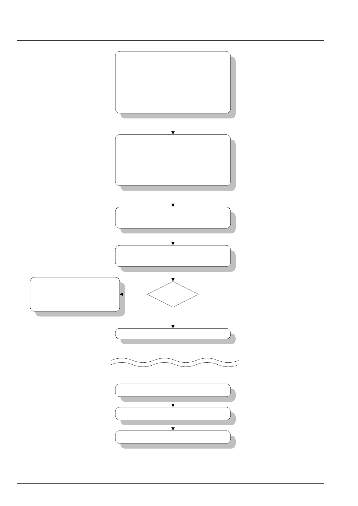
MSP 34x1G PRELIMINARY DATA SHEET
Write MODUS Register
Example
[0] = 1 Automatic Sound Select = on
[1] = 1 Enable interrupt if STATUS changes
[8] = 0 ANA_IN1+ is selected
Define Preference for Automatic Standard
Detection:
[12] = 0 If 6.5 MHz, set SECAM-L
[14:13] = 3 Ignore 4.5 MHz carrier
for the essential bits:
:
Write SOURCE SELECT Settings
Example:
set loudspeaker Source Select to "Stereo or A"
set headphone Source Select to "Stereo or B"
set SCART_Out Source Select to "Stereo or A/B"
set Channel Matrix mode for all outputs to "Stereo"
Write FM/AM-Prescale
Write NICAM-Prescale
set previous standard or
set standard manually according
picture information
In case of MSPG-
Interrupt to Controller:
Write 01 into
STANDARD SELECT Register
(Start Automatic Standard Detection)
yes
Result = 0
?
no
expecting MSPG-interrupt
Read STATUS
Adjust TV-Display
If Bilingual, adjust Source Select setting if required
Fig. 3–2: Software flow diagram for a Minimum demodulator setup for a European Multistandard TV set applying the
Automatic Sound Select feature
46 MICRONAS INTERMETALL
Page 47

PRELIMINARY DATA SHEET MSP 34x1G
4. Specifications
4.1. Outline Dimensions
619
60
9
44
4327
0.12±
25.14
1
10
2
9
26
0.12±
25.14
Fig. 4–1:
68-Pin Plastic Leaded Chip Carrie r Pack age
(PLCC68)
Weight approximately 4.8 g
Dimensions in mm
0.2±
x 45 °1.1
±0.05
1.9
±0.1
4.05
±0.15
4.75
0.05±
0.71
0.04±
0.23
0.06±
0.48
0.9
0.3±
23.3
0.1
0.1±
24.2
16 x 1.27 = 20.32
1.27
2
24.2
0.1±
1.2 x 45°
1.27
7.5
7.5
0.1±
SPGS0027-2(P68)/1E
0.1±
16 x 1.27 = 20.32
0.28
±0.06
SPGS0016-5(P64)/1E
±0.1
19.3
±0.05
18
±0.5
20.3
3364
132
57.7
1
1.778
31 x 1.778 = 55.1
±0.1
±0.05
±0.1
0.48
±0.06
±0.1
±0.2
3.8
0.8
±0.2
3.2
Fig. 4–2:
64-Pin Plastic Shrink Dual-Inline Package
(PSDIP64)
Weight approximately 9.0 g
Dimensions in mm
2752
126
47.0
1
1.778
25 x 1.778 = 44.4
±0.1
±0.05
±0.1
0.48
±0.06
±0.2
0.6
±0.1
4.0
±0.2
2.8
SPGS0016-5(P52)/1E
15.6
14
±0.06
0.28
16.3
Fig. 4–3:
52-Pin Plastic Shrink Dual-Inline Package
(PSDIP52)
Weight approximately 5.5 g
Dimensions in mm
±0.1
±0.1
±1
MICRONAS INTERMETALL 47
Page 48

MSP 34x1G PRELIMINARY DATA SHEET
65
8
0.15±
0.15±
17.2
80
1.8
10.3
9.8
16
23.2
Fig. 4–4:
80-Pin Plastic Quad Flat Pack
(PQFP80)
Weight approximately 1.61 g
Dimensions in mm
3348
49
0.2±
12
64
1.75
116
1.75
12
0.2±
32
17
4164
241
0.145
1.5
0.04±
0.17
40
0.05±
0.37
25
0.05±
1.3
±0.2
3
0.055±
0.1±
0.05±
0.22
0.05±
1.4
0.1
0.1±
10
0.1±
2.7
0.1
15 x 0.5 = 7.5
0.5
10
0.1±
14
0.1±
0.5
0.1±
0.8
1.8
23 x 0.8 = 18.4
20
0.1±
15 x 0.5 = 7.5
0.1±
0.1±
8
5
0.1±
SPGS705000-1(P80)/1E
0.8
15 x 0.8 = 12.0
Fig. 4–5:
64-Pin Plastic Low-Profile Quad Flat Pack
(PLQFP64)
Weight approximately 3.5 g
Dimensions in mm
D0025/3E
48 MICRONAS INTERMETALL
Page 49

PRELIMINARY DATA SHEET MSP 34x1G
4.2. Pin Connections and Short Descriptions
NC = not connected; leave vacant
LV = if not used, leave vacant
OBL = obligatory; connect as described in circuit diagram
DVSS: if not used, connect to DVSS
AHVSS: connect to AHVSS
PLCC
68-pin
PSDIP
64-pin
Pin No. Pin Name Type Connection
PSDIP
52-pin
PQFP
80-pin
PLQFP
64-pin
(if not used)
Short Description
1 16 14 9 8 ADR_WS OUT LV ADR word strobe
2
−−−−
NC LV Not connected
3 15 13 8 7 ADR_DA OUT LV ADR data output
2
4 14127 6 I2S_DA_IN1 IN LV I
5 13 1 1 6 5 I2S_DA_OUT OUT L V I
6 12105 4 I2S_WS IN/OUTLV I
711943I2S_CL IN/OUTLV I
8 10 8 3 2 I2C_DA IN/OUT OBL I
99721I2C_CL IN/OUTOBL I
10 8
−
1 64 NC LV Not connected
S1 data input
2
S data output
2
S word strobe
2
S clock
2
C data
2
C clock
11 7 6 80 63 STANDBYQ IN OBL Stand-by (low -active)
2
12657962ADR_SEL IN OBL I
C Bus address select
13 5 4 78 61 D_CTR_I/O_0 IN/OUT LV D_CTR_I/O_0
14 4 3 77 60 D_CTR_I/O_1 IN/OUT LV D_CTR_I/O_1
15 3
16 2
17
−
−
−−−−
76 59 NC LV Not connected
75 58 NC LV Not connected
NC LV Not connected
18 1 2 74 57 AUD_CL_OUT OUT LV Audio clock output
(18.432 MHz)
19 64 1 73 56 TP LV Test pin
20 63 52 72 55 XTAL_OUT OUT OBL Crystal oscillator
21 62 51 71 54 XT AL_IN IN OBL Crystal oscillator
22 61 50 70 53 TESTEN IN OBL Test pin
23 60 49 69 52 ANA_IN2
24 59 48 68 51 ANA_IN
+
IN AVSS via
56 pF / LV
−
IN AVSS via
56 pF / LV
IF input 2
vacant, only if IF input 1 is
also not in use)
IF common (can be left
vacant, only if IF input 1 is
also not in use)
(can be left
MICRONAS INTERMETALL 49
Page 50

MSP 34x1G PRELIMINARY DATA SHEET
Pin No. Pin Name Type Connection
PLCC
68-pin
PSDIP
64-pin
PSDIP
52-pin
PQFP
80-pin
PLQFP
64-pin
25 58 47 67 50 ANA_IN1
(if not used)
+
IN LV IF input 1
Short Description
26 57 46 66 49 AVSUP OBL Analog power supply 5 V
−−−
−−−
−−−
65
64
63
−
−
−
AVSUP OBL Analog power supply 5 V
NC LV Not connected
NC LV Not connected
27 56 45 62 48 A VSS OBL Analog ground
−−−
61
−
AVSS OBL Analog ground
28 55 44 60 47 MONO_IN IN LV Mono input
−−−
59
−
NC LV Not connected
29 54 43 58 46 VREFTOP OBL Reference voltage IF
A/D converter
30 53 42 57 45 SC1_IN_R IN LV SCART 1 input, right
31 52 41 56 44 SC1_IN_L IN LV SCART 1 input, left
32 51
−
55 43 ASG1 AHVSS Analog Shield Ground 1
33 50 40 54 42 SC2_IN_R IN LV SCART 2 input, right
34 49 39 53 41 SC2_IN_L IN LV SCART 2 input, left
35 48
−
52 40 ASG2 AHVSS Analog Shield Ground 2
36 47 38 51 39 SC3_IN_R IN LV SCART 3 input, right
37 46 37 50 38 SC3_IN_L IN LV SCART 3 input, left
38 45
39 44
40 43
41
−−
−
−
−
49 37 ASG4 AHVSS Analog Shield Ground 4
48 36 SC4_IN_R IN LV SCART 4 input, right
47 35 SC4_IN_L IN LV SCART 4 input, left
46
−
NC LV or AHVSS Not connected
42 42 36 45 34 AGNDC OBL Analog reference
voltage
43 41 35 44 33 AHVSS OBL Analog ground
−−−
−−−
43
42
−
−
AHVSS OBL Analog ground
NC LV Not connected
−−−
41
−
NC LV Not connected
44 40 34 40 32 CAPL_M OBL Volume capacitor MAIN
45 39 33 39 31 AHVSUP OBL Analog power supply 8 V
46 38 32 38 30 CAPL_A OBL Volume capacitor AUX
50 MICRONAS INTERMETALL
Page 51
PRELIMINARY DATA SHEET MSP 34x1G
PLCC
68-pin
PSDIP
64-pin
Pin No. Pin Name Type Connection
PSDIP
52-pin
PQFP
80-pin
PLQFP
64-pin
(if not used)
Short Description
47 37 31 37 29 SC1_OUT_L OUT LV SCART output 1, left
48 36 30 36 28 SC1_OUT_R OUT LV SCART output 1, right
49 35 29 35 27 VREF1 OBL Reference ground 1
50 34 28 34 26 SC2_OUT_L OUT LV SCART output 2, left
51 33 27 33 25 SC2_OUT_R OUT LV SCART output 2, right
52
−−
53 32
−
32
−
NC LV Not connected
31 24 NC LV Not connected
54 31 26 30 23 DACM_SUB OUT LV Subwoofer output
55 30
−
29 22 NC LV Not connected
56 29 25 28 21 DACM_L OUT LV Loudspeaker out, left
57 28 24 27 20 DACM_R OUT LV Loudspeaker out, right
58 27 23 26 19 VREF2 OBL Reference ground 2
59 26 22 25 18 DACA_L OUT LV Headphone out, left
60 25 21 24 17 DACA_R OUT LV Headphone out, right
−−−
−−−
23
22
−
−
NC LV Not connected
NC LV Not connected
61 24 20 21 16 RESETQ IN OBL Power-on-reset
62 23
63 22
−
−
20 15 NC LV Not connected
19 14 NC LV Not connected
64 21 19 18 13 NC LV Not connected
2
65 20 18 17 12 I2S_DA_IN2 IN LV I
S2-data input
66 19 17 16 11 DVSS OBL Digital ground
−−−
−−−
15
14
−
−
DVSS OBL Digital ground
DVSS OBL Digital ground
67 18 16 13 10 DVSUP OBL Digital power supply 5 V
−−−
12
−
DVSUP OBL Digital power supply 5 V
−−−
11
−
DVSUP OBL Digital power supply 5 V
68 17 15 10 9 ADR_CL OUT LV ADR clock
1)
Due to the compatibility with MSP 3410B, it is possible to connect with DVSS as well.
MICRONAS INTERMETALL 51
Page 52

MSP 34x1G PRELIMINARY DATA SHEET
4.3. Pin Descriptions
Pin numbers refer to the 80-pin PQFP package.
Pin 1, NC – Pin not connected.
2
Pin 2, I2C_CL – I
Via this pin, the I
C Clock Input/Output (Fig. 4–12)
2
C-bus clock signal has to be supplied. The signal can be pulled down by the MSP in
case of wait conditions.
2
Pin 3, I2C_DA – I
Via this pin, the I
C Data Input/Output (Fig. 4–12)
2
C-bus data is written to or read from
the MSP.
2
Pin 4, I2S_CL – I
Clock line for the I
driven by the MSP; in slave mode, an external I
S Clock Input/Output (Fig. 4–15)
2
S bus. In master mo de, this line is
2
clock has to be supplied.
2
Pin 5, I2S_WS – I
(Fig. 4–15)
Word strobe line for the I
line is driven by the MSP; in slave mod e, an external
2
S word strobe has to be supplied.
I
Pin 6, I2S_DA_OUT – I
Output of digital serial sound data of the MSP on the
2
S bus.
I
Pin 7, I2S_DA_IN1 – I
First input of digital se rial sound data to the MSP via
2
S bus.
the I
S Word Strobe Input/Output
2
S bus. In master mode, this
2
S Data Output (Fig. 4–11)
2
S Data Input 1 (Fig. 4–13)
Pin 8, ADR_DA – ADR Bus Data Output (Fig. 4–11)
Output of digital serial data to the DRP 3510A via the
ADR bus.
Pin 9, ADR_WS – ADR Bus Word Strobe Output
(Fig. 4–11)
Word strobe output for the ADR bus.
Pin 10, ADR_CL – ADR Bus Clock Output (Fig. 4–11)
Clock line for the ADR bus.
Pins 11, 12, 13, DVSUP* – Digital Supply Voltage
Power supply for the digital circuit ry of the MSP. Must
be connected to a +5 V power supply.
Pins 14, 15, 16, DVSS* – Digital Ground
Ground connection for the digital circuitry of the MSP.
2
Pin 17, I2S_DA_IN2 – I
Second input of digita l serial sound data to the MSP
via the I
2
S bus.
S Data Input 2 (Fig. 4–13)
Pins 22, 23, NC – Pins not connected.
Pins 24, 25, DACA_R/L – Headphone Outputs
(Fig. 4–21)
Output of the headphone signal. A 1-nF capacitor to
AHVSS must be connected to these pins. The DC offset on these pins dep end s o n th e s ele cted headphone
volume.
Pin 26, VREF2 – Reference Ground 2
Reference analog groun d. This pi n mus t be co nne cte d
separately to the single ground point (AHVSS). VREF2
serves as a clean gro und and should be used as the
reference for analog connections to the loudspeaker
and headphone outputs.
S
Pins 27, 28, DACM_R/L – Loudspeaker Outputs
(Fig. 4–21)
Output of the lo udspeaker signal. A 1 -nF capacitor to
AHVSS must be connected to these pins. The DC offset on these pins depends on the selected loudspeaker volum e.
Pin 29, NC – Pin not connected.
Pin 30, DACM_SUB – Subwoofer Output (Fig. 4–21)
Output of the subwoofer signal. A 1-nF capacitor to
AHVSS must be conn ected to this pi n. Due to the l ow
frequency content of th e subwoofer output, the value
of the capacitor may be increased for better s uppression of high-frequency noise. The DC offset on this pin
depends on the selected loudspeaker volume.
Pins 31, 32 NC – Pin not connected.
Pins 33, 34, SC2_OUT_R/L – SCART2 Outputs
(Fig. 4–23)
Output of the SCART2 signal. Connections to these
pins must use a 100-Ω series resistor and are intended
to be AC-coupled.
Pin 35, VREF1 – Reference Ground 1
Reference analog groun d. This pi n mus t be co nne cte d
separately to the single ground point (AHVSS). VREF1
serves as a clean gro und and should be used as the
reference for analog connections to the SCART outputs.
Pins 36, 37, SC1_OUT_R/L – SCART1 Outputs
(Fig. 4–23)
Output of the SCART1 signal. Connections to these
pins must use a 100-Ω series resistor and are intended
to be AC-coupled.
Pins 18, 19, 20, NC – Pins not connected.
Pin 21, RESETQ – Reset Input (Fig. 4–13)
In the steady s tate, high level is required. A low lev el
resets the MSP 34x1G.
52 MICRONAS INTERMETALL
Page 53

PRELIMINARY DATA SHEET MSP 34x1G
Pin 38, CAPL_A – Volume Capacitor Headphone
(Fig. 4–18)
A 10-µF capacitor to AHVSU P must be connected to
this pin. It serves a s a smoothing filter for headphone
volume changes in order to suppress audible plops.
The value of the capac itor can be lowered to 1-µF if
faster response is requir ed. The area encircl ed by the
trace lines sho uld be minimized; keep traces as short
as possible. T his input is sensiti ve for mag netic indu ction.
Pin 39, AHVSUP* – Analog Power Supply High Voltage
Power is supplied via this pin for the analog circuitry of
the MSP (except IF input). This pin must be connected
to the +8 V supply.
Pin 40, CAPL_M – Volume Capacitor Loudspeaker
(Fig. 4–18)
A 10-µF capacitor to AHVSU P must be connected to
this pin. It serves as a smo othing filter for lou dspeak er
volume changes in order to suppress audible plops.
The value of th e capacitor can be lowered to 1µF if
faster response is requir ed. The area encircl ed by the
trace lines sho uld be minimized; keep traces as short
as possible. T his input is sensiti ve for mag netic indu ction.
Pins 41, 42, NC – Pins not connected.
Pins 43, 44, AHVSS* – Analog Power Supply High
Vol tag e
Ground connection for the analog c ircuitry o f the MS P
(except IF input).
Pin 45, AGNDC – Internal Analog Reference Voltage
This pin serves as the internal ground conne ction for
the analog circuitry ( except IF input). It must be connected to the VREF pins with a 3.3-µF and a 100-nF
capacitor in pa r al le l. Th is pi ns sh ow s a DC le ve l of t yp ically 3.73 V.
Pin 46, NC – Pin not connected.
Pins 47, 48, SC4_IN_L/R – SCART4 Inputs
(Fig. 4–20)
The analog input s ignal for SCART4 is fe d to this pin.
Analog input connection must be AC-coupled.
Pin 49, ASG4 – Analog Shield Ground 4
Analog ground (AHVSS ) should be connected to this
pin to reduce cross-coupling between SCART inputs.
Pins 50, 51, SC3_IN_L/R – SCART3 Inputs
(Fig. 4–20)
The analog input s ignal for SCART3 is fe d to this pin.
Analog input connection must be AC-coupled.
Pins 53, 54 SC2_IN_L/R – SCART2 Inputs (Fig. 4–20)
The analog input s ignal for SCART2 is f ed to this pin.
Analog input connection must be AC-coupled.
Pin 55, ASG1 – Analog Shield Ground 1
Analog ground (AHVSS ) should be connected to this
pin to reduce cross-coupling between SCART inputs.
Pins 56, 57 SC1_IN_L/R – SCART1 Inputs (Fig. 4–20)
The analog input s ignal for SCART1 is f ed to this pin.
Analog input connection must be AC-coupled.
Pin 58, VREFTOP – Reference Voltage IF A/D Con-
verter (Fig. 4–17)
Via this pin, the referenc e voltage for the IF A/D con verter is decoupled. It must be connected to AVSS
pins with a 10-µF and a 100-nF ca pacitor in parallel.
Traces must be kept short.
Pin 59, NC – Pin not connected.
Pin 60 MONO_IN – Mono Input (Fig. 4–20)
The analog mono inpu t si gna l i s fe d to th is pi n. A nalog
input connection must be AC-coupled.
Pins 61, 62, AVSS* – Analog Power Supply Voltage
Ground connection for the analog IF input circuitry of
the MSP.
Pins 63, 64, NC – Pins not connected.
Pins 65, 66, AVSUP* – Analog Power Supply Voltage
Power is supplied via thi s pin for the analog IF input
circuitry of the MSP. This pin must be connected to the
5V supply.
+
Pin 67, ANA_IN1+ – IF Input 1 (Fig. 4–17)
The analog sound IF signal is supplied to this pin.
Inputs must be AC-coupled. This pin is designed as
symmetrical input: ANA_IN1+ is internally connected
to one input of a sy mmetrical op amp, ANA_IN- to the
other.
Pin 68, ANA_IN− – IF Common (Fig. 4–17)
This pins serves as a common reference for ANA_IN1/
2+ inputs.
Pin 69, ANA_IN2+ – IF Input 2 (Fig. 4–17)
The analog sound if signal is supplied to this pin.
Inputs must be AC-coupled. This pin is designed as
symmetrical input: ANA_IN2+ is internally connected
to one input of a sy mmetr ica l op amp, ANA_IN− to the
other.
Pin 70, TESTEN – Test Enable Pin (Fig. 4–13)
This pin enables factory test modes. For normal operation, it must be connected to ground.
Pin 52, ASG2 – Analog Shield Ground 2
Analog ground (AHVSS ) should be connected to this
pin to reduce cross-coupling between SCART inputs.
MICRONAS INTERMETALL 53
Page 54

MSP 34x1G PRELIMINARY DATA SHEET
Pins 71, 72 XTAL_IN, XTAL_OUT – Crystal Input and
Output Pins (Fig. 4–16)
These pins are connected to an 18.432 MHz crystal
oscillator which is digitally tuned by integrated shunt
capacitances. An external clock can be fed into
XTAL_IN. The audio clock output signal
AUD_CL_OUT is derived from the osci llator. External
capacitors at each crystal pin to ground (AVSS) are
required. It shou ld be v er ified by lay ou t, that no s upp ly
current for the digital circuitry is flowing through the
ground connection point.
Pin 73, TP – This pin enables fac tory test modes. For
normal operation, it must be left vacant.
Pin 74, AUD_CL_OUT – Audio Clock Output
(Fig. 4–16)
This is the 18.432 MHz main clock output.
Pins 75, 76, NC – Pins not connected.
Pins 77, 78, D_CTR_I/O_1/0 – Digital Control Input/
Output Pins (Fig. 4–15)
These pins serve as general purpose input/output
pins. Pin D_CTR_I/O_1 can be used as an interrupt
request pin to the controller.
2
Pin 79, ADR_SEL – I
C Bus Address Select
(Fig. 4–14)
By means of this pin, one o f three device addresses
for the MSP can be selected. The pin can be connected to ground (I
5 V supply (84/85
+
2
C device addresses 80/81
), or left open (88/89
hex
hex
), to
hex
).
Pin 80, STANDBYQ – Stand-by
In normal operation, this pin must be High. If the
MSP 34x1G is swi tch ed o ff by fir s t pu ll ing STANDBYQ
low and then (after > 1µs delay) swi tching off the 5 V,
but keeping the 8-V po wer supp ly (‘Stand-by’-mode),
the SCART switches maintai n their position and fun ction.
* Application Note:
All ground pins sh ould be conne cted to one low -resistive ground plane. All supply pins should be connected
separately with short and low-resistive lines to the
power supply. Decoupling capacitors from D VSUP to
DVSS, AVSUP to AVSS, and AHVS UP to AHVSS are
recommended as closely as possible to these pins.
Decoupling of DVSUP and DVSS is most important.
We recommend using more than one capacitor. By
choosing different values, the frequency range of
active decoupl ing can be ext ended. In our app lication
boards we use: 220 pF, 470 pF, 1.5 nF, and 10µF. The
capacitor with the lowes t v al ue sh oul d b e plac ed near est to the DVSUP and DVSS pins.
54 MICRONAS INTERMETALL
Page 55

PRELIMINARY DATA SHEET MSP 34x1G
4.4. Pin Configurations
ADR_WS
NC
ADR_DA
I2S_DA_IN1
I2S_DA_OUT
I2S_WS
I2S_CL
I2C_DA
I2C_CL
9876543216867666564636261
10
NC
STANDBYQ
ADR_SEL
D_CTR_I/O_0
D_CTR_I/O_1
AUD_CL_OUT
XTAL_OUT
XTAL_IN
TESTEN
ANA_IN2+
ANA_IN−
ANA_IN1+
11
12
13
14
15
NC
16
NC
17
NC
18
19
TP
20
21
22
23
24
25
26 44
AVSUP CAPL_M
27 28 29 30 31 32 33 34 35 36 37 38 39 40 41 42 43
MSP 34x1G
ADR_CL
DVSUP
DVSS
I2S_DA_IN2
NC
NC
NC
RESETQ
60
59
58
57
56
55
54
53
52
51
50
49
48
47
46
45
DACA_R
DACA_L
VREF2
DACM_R
DACM_L
NC
DACM_SUB
NC
NC
SC2_OUT_R
SC2_OUT_L
VREF1
SC1_OUT_R
SC1_OUT_L
CAPL_A
AHVSUP
AVSS
MONO_IN
VREFTOP
SC1_IN_R
SC1_IN_L
ASG1
SC2_IN_R
SC2_IN_L
Fig. 4–6: 68-pin PLCC package
AHVSS
AGNDC
NC
SC4_IN_L
SC4_IN_R
ASG4
SC3_IN_L
SC3_IN_R
ASG2
MICRONAS INTERMETALL 55
Page 56

MSP 34x1G PRELIMINARY DATA SHEET
1AUD_CL_OUT
2NC
3NC
4D_CTR_I/O_1
5D_CTR_I/O_0
6ADR_SEL
7STANDBYQ
8NC
9I2C_CL
10I2C_DA
11I2S_CL
12I2S_WS
13I2S_DA_OUT
14I2S_DA_IN1
15ADR_DA
16ADR_WS
TP64
XTAL_OUT63
XTAL_IN62
TESTEN61
ANA_IN2+60
ANA_IN−59
ANA_IN+58
AVSUP57
AVSS56
MONO_IN55
VREFTOP54
SC1_IN_R53
SC1_IN_L52
ASG151
SC2_IN_R50
SC2_IN_L49
17ADR_CL
18DVSUP
19DVSS
20I2S_DA_IN2
21NC
22NC
23NC
24RESETQ
25DACA_R
26DACA_L
ASG248
SC3_IN_R47
SC3_IN_L46
ASG445
SC4_IN_R44
SC4_IN_L43
AGNDC42
AHVSS41
CAPL_M40
AHVSUP39
MSP 34x1G
VREF2
DACM_R
DACM_L
NC
DACM_SUB
NC
38
37
36
35
34
33
27
28
29
30
31
32
CAPL_A
SC1_OUT_L
SC1_OUT_R
VREF1
SC2_OUT_L
SC2_OUT_R
AUD_CL_OUT
D_CTR_I/O_1
D_CTR_I/O_0
ADR_SEL
STANDBYQ
I2C_CL
I2C_DA
I2S_CL
I2S_WS
I2S_DA_OUT
I2S_DA_IN1
ADR_DA
ADR_WS
ADR_CL
DVSUP
DVSS
I2S_DA_IN2
NC
RESETQ
DACA_R
DACA_L
VREF2
DACM_R
DACM_L
DACM_SUB
1
TP
2
3
4
5
6
7
8
9
10
11
12
13
14
15
16
17
18
19
20
21
22
23
24
25
26
MSP 34x1G
52
51
50
49
48
47
46
45
44
43
42
41
40
39
38
37
36
35
34
33
32
31
30
29
28
27
XTAL_OUT
XTAL_IN
TESTEN
ANA_IN2+
ANA_IN−
ANA_IN1+
AVSUP
AVSS
MONO_IN
VREFTOP
SC1_IN_R
SC1_IN_L
SC2_IN_R
SC2_IN_L
SC3_IN_R
SC3_IN_L
AGNDC
AHVSS
CAPL_M
AHVSUP
CAPL_A
SC1_OUT_L
SC1_OUT_R
VREF1
SC2_OUT_L
SC2_OUT_R
Fig. 4–8: 52-pin PSDIP package
Fig. 4–7: 64-pin PSDIP package
56 MICRONAS INTERMETALL
Page 57

PRELIMINARY DATA SHEET MSP 34x1G
SC2_IN_L ASG2
AVSUP
AVSUP
ANA_IN1+
ANA_IN−
ANA_IN2+
TESTEN
XTAL_IN
XTAL_OUT
AUD_CL_OUT
NC
NC
D_CTR_I/O_1
D_CTR_I/O_0
ADR_SEL
STANDBYQ
SC2_IN_R
ASG1
SC1_IN_L
SC1_IN_R
VREFTOP
NC
MONO_IN
AVSS
AVSS
NC
NC
64 63 62 61 60 59 58 57 56 55 54 53 52 51 50 49 48 47 46 45 44 43 42 41
65
66
67
68
69
70
71
72
73
TP
74
75
76
77
78
79
80
1 2 3 4 5 6 7 8 9 101112131415161718192021222324
MSP 34x1G
SC3_IN_R
SC3_IN_L
ASG4
SC4_IN_R
SC4_IN_L
NC
AGNDC
AHVSS
AHVSS
NC
NC
40
39
38
37
36
35
34
33
32
31
30
29
28
27
26
25
CAPL_M
AHVSUP
CAPL_A
SC1_OUT_L
SC1_OUT_R
VREF1
SC2_OUT_L
SC2_OUT_R
NC
NC
DACM_SUB
NC
DACM_L
DACM_R
VREF2
DACA_L
NC
I2C_CL
I2C_DA
I2S_CL
I2S_WS
I2S_DA_OUT
I2S_DA_IN1
ADR_DA
ADR_WS
ADR_CL
Fig. 4–9: 80-pin PQFP package
DVSUP
DVSUP DVSUP
DACA_R
NC
NC
RESETQ
NC
NC
NC
I2S_DA_IN2
DVSS
DVSS
DVSS
MICRONAS INTERMETALL 57
Page 58

MSP 34x1G PRELIMINARY DATA SHEET
AVSUP
ANA_IN1+
ANA_IN−
ANA_IN2+
TESTEN
XTAL_IN
XTAL_OUT
AUD_CL_OUT
NC
NC
D_CTR_I/OUT1
D_CTR_I/OUT0
ADR_SEL
STANDBYQ
NC
SC2_IN_L
SC2_IN_R
ASG1
SC1_IN_L
SC1_IN_R
VREFTOP
MONO_IN
AVSS
48 47 46 45 44 43 42 41 40 39 38 37 36 35 34 33
49
50
51
52
53
54
55
TP
56
57
58
59
60
61
62
63
64
12345678910111213141516
MSP 34x1G
ASG2
SC3_IN_R
SC3_IN_L
ASG4
SC4_IN_R
SC4_IN_L
AGNDC
AHVSS
32
31
30
29
28
27
26
25
24
23
22
21
20
19
18
17
CAPL_M
AHVSUP
CAPL_A
SC1_OUT_L
SC1_OUT_R
VREF1
SC2_OUT_L
SC2_OUT_R
NC
DACM_SUB
NC
DACM_L
DACM_R
VREF2
DACA_L
DACA_R
I2C_CL
I2C_DA
I2S_CL
I2S_WS
I2S_DA_OUT
I2S_DA_IN1
ADR_DA
ADR_WS
Fig. 4–10: 64-pin PLQFP package
RESETQ
NC
NC
NC
I2S_DA_IN2
DVSS
DVSUP
ADR_CL
58 MICRONAS INTERMETALL
Page 59
PRELIMINARY DATA SHEET MSP 34x1G
4.5. Pin Circuits
Pin numbers refer to the PQFP80 package.
DVSUP
P
N
GND
Fig. 4–11: Output Pins 6, 8, 9, and 10
(I2S_DA_OUT, ADR_DA, ADR_WS, ADR_CL)
N
GND
Fig. 4–12: Input/Output Pins 2 and 3
(I2C_CL, I2C_DA)
DVSUP
P
N
GND
Fig. 4–15: Input/Output Pins 4, 5, 77, and 78
(I2S_CL, I2S_WS, D_CTR_I/O_1, D_CTR_I/O_0)
P
500 k
3−30 pF
3−30 pF
Ω
N
2.5 V
Fig. 4–13: Input Pins 7, 17, 21, 70, and 80
(I2S_DA_IN1, I2S_DA_IN2, RESETQ, TESTEN,
STANDBYQ)
DVSUP
23 k
Ω
23 k
Ω
GND
ADR_SEL
Fig. 4–14: Input Pin 79 (ADR_SEL)
Fig. 4–16: Output/Input Pins 71, 72, and 74
(XTAL_IN, XTAL_OUT, AUD_CL_OUT)
ANA_IN1+
ANA_IN2+
ANA_IN
−
VREFTOP
Fig. 4–17: Input Pins 58, 67, 68, and 69
(VREFTOP, ANA_IN1+, ANA_IN-, ANA_IN2+)
A
D
MICRONAS INTERMETALL 59
Page 60
MSP 34x1G PRELIMINARY DATA SHEET
0...2 V
≈
3.75 V
24 k
Ω
≈
3.75 V
40 k
Ω
AHVSUP
0...1.2 mA
3.3 k
Ω
125 k
Ω
3.75 V
≈
Fig. 4–18: Capacitor Pins 38 and 40
(CAPL_A, CAPL_M)
Fig. 4–19: Input Pin 60 (MONO_IN)
Fig. 4–20: Input Pins 47, 48, 50, 51, 53, 54, 56, and 57
(SC4-1_IN_L/R)
Fig. 4–22: Pin 45 (AGNDC)
26 pF
120 k
Ω
300
Ω
3.75 V
≈
Fig. 4–23: Output Pins 33, 34, 36, and 37
(SC_2_OUT_R/L, SC_1_OUT_R/L)
Fig. 4–21: Output Pins 24, 25, 27, 28 and 30
(DACA_R/L, DACM_R/L, DACM_SUB)
60 MICRONAS INTERMETALL
Page 61

PRELIMINARY DATA SHEET MSP 34x1G
4.6. Electrical Characteristics
4.6.1. Absolute Maximum Ratings
Symbol Parameter Pin Name Min. Max . Unit
T
T
V
V
V
dV
P
V
I
Idig
V
I
Iana
A
S
TOT
SUP1
SUP2
SUP3
SUP23
Idig
Iana
Ambient Operating Temperature
Storage Temperature
−
−−
First Supply Voltage AHVSUP
Second Supply Voltage DVSUP
Third Supply Voltage AVSUP
Voltage between AVSUP
and DVSUP
Power Dissipation
PLCC68
PSDIP64
AVSUP,
DVSUP
AHVSUP,
DVSUP,
AVSUP
PSDIP52
PQFP80
PLQFP64
Input Voltage, all Digital Inputs
Input Current, all Digital Pins
−−
Input Voltage, all Analog Inputs SCn_IN_s,
MONO_IN
Input Current, all Analog Inputs SCn_IN_s,
MONO_IN
0701)°
40 125
0.3 9.0 V
−
0.3 6.0 V
−
0.3 6.0 V
−
0.5 0.5 V
−
1200
1300
1200
1000
1)
960
0.3 V
−
20
3)
3)
0.3 V
−
5
−
+
+
0.3 V
+
SUP2
20 mA
0.3 V
+
SUP1
5mA
C
C
°
mW
mW
mW
mW
mW
2)
2)
I
Oana
I
Oana
Output Current, all SCART Outputs SCn_OUT_s
Output Current, all Analog Outputs
DACp_s
3) 4), 5) 4), 5)
3) 4) 4)
except SCART Outputs
I
Cana
1)
PLQFP64: 65 °C
2)
positive value means current flowing into the circuit
3)
“n” means “1”, “2”, “3”, or “4”, “s” means “L” or “R”, “p” means “M” or “A”
4)
The analog outputs are short-circuit proof with respect to First Supply Voltage and ground.
5)
Total chip power dissipation must not exceed absolute maximum rating.
Output Current, other pins
connected to capacitors
CAPL_p,
AGNDC
3)
4) 4)
Stresses beyond those listed in the “Absolute Maximum Ratings” may cause permanent damage to the device. This
is a stress rating only. Functional operation of the dev ice at the se or any othe r conditi ons beyond those ind icate d in
the “Recommended Operating Con ditions/Char acteristic s” of this sp ecification i s not impli ed. Exposu re to absolute
maximum ratings conditions for extended periods may affect device reliability.
MICRONAS INTERMETALL 61
Page 62

MSP 34x1G PRELIMINARY DATA SHEET
4.6.2. Recommended Operating Conditions (TA = 0 to 70 °C)
4.6.2.1. General Recommended Operating Conditions
Symbol Parameter Pin Name Min. Typ. M ax. Unit
V
SUP1
First Supply Voltage
AHVSUP 7.6 8.0 8.7 V
(8-V Operation)
First Supply Voltage
4.75 5.0 5.25 V
(5-V Operation)
V
SUP2
V
SUP3
t
STBYQ1
Second Supply Voltage DVSUP 4.75 5.0 5.25 V
Third Supply Voltage AVSUP 4.75 5.0 5.25 V
STANDBYQ Setup Time before
Turn-off of Second Supply Voltage
STANDBYQ,
DVSUP
1
4.6.2.2. Analog Input and Output Recommendations
Symbol Parameter Pin Name Min. Typ. M ax. Unit
C
AGNDC
C
inSC
AGNDC-Filter-Capacitor AGNDC
Ceramic Capacitor in Parallel
DC-Decoupling Capacitor in front of
SCn_IN_s
1)
20% 3.3
−
20% 100 nF
−
20% 330 nF
−
SCART Inputs
s
µ
F
µ
V
inSC
V
inMONO
R
LSC
C
LSC
C
VMA
SCART Input Level 2.0 V
Input Level, Mono Input MONO_IN 2.0 V
SCART Load Resistance SCn_OUT_s
SCART Load Capacitance 6.0 nF
Main/AUX Volume Capacitor CAPL_M,
CAPL_A
C
FMA
1)
“n” means “1”, “2”, or “3”, “s” means “L” or “R”, “p” means “M” or “A”
Main/AUX Filter Capacitor DACM_s,
DACA_s
1)
RMS
RMS
1)
10 k
10
10% 1
−
10% nF
+
Ω
F
µ
62 MICRONAS INTERMETALL
Page 63

PRELIMINARY DATA SHEET MSP 34x1G
4.6.2.3. Recommendations for Analog Sound IF Input Signal
Symbol Parameter Pin Name Min. Typ. Max. Unit
C
VREFTOP
F
IF_FMTV
F
IF_FMRADIO
V
IF_FM
V
IF_AM
R
FMNI
R
AMNI
R
FM
R
FM1/FM2
VREFTOP-Filter-Capacitor VREFTOP
Ceramic Capacitor in Parallel
Analog Input Frequency Range
for TV Applications
ANA_IN1+,
ANA_IN2+,
ANA_IN
−
Analog Input Frequency for
20 % 10
−
20 % 100 nF
−
µ
09MHz
10.7 MHz
FM-Radio Applications
Analog Input Range FM/NICAM 0.1 0.8 3 V
Analog Input Range AM/NICAM 0.1 0.45 0.8 V
Ratio: NICAM Carrier/FM Carrier
(unmodulated carriers)
BG:
I:
Ratio: NICAM Carrier/AM Carrier
20
−
23
−
25
−
7
−
10
−
11 0 dB
−
0
0
dB
dB
(unmodulated carriers)
Ratio: FM-Main/FM-Sub Satellite 7 dB
Ratio: FM1/FM2
7dB
German FM-System
F
pp
pp
R
FC
R
FV
PR
SUP
FM
IF
HF
MAX
Ratio: Main FM Carrier/
Color Carrier
Ratio: Main FM Carrier/
Luma Components
Passband Ripple
Suppression of Spectrum
above 9.0 MHz (not for FM Radio)
Maximum FM-Deviation (approx.)
normal mode
HDEV2: high deviation mode
HDEV3: very high deviation mode
15
15
−−±
15
−−
−−
2dB
−
180
±
360
±
540
±
dB
dB
dB
kHz
kHz
kHz
MICRONAS INTERMETALL 63
Page 64
MSP 34x1G PRELIMINARY DATA SHEET
4.6.2.4. Crystal Recommendati ons
Symbol Parameter Pin Name Min. Typ. M ax. Unit
General Crystal Recommendations
f
P
Crystal Parallel Resonance Frequency at 12 pF Load Capacitance
R
R
C
0
C
L
Crystal Series Resistance 8 25
Crystal Shunt (Paralle l) Cap acit an ce 6.2 7.0 pF
External Load Capacitance
1)
XTAL_IN,
XTAL_OUT
Crystal Recommendations for Master-Slave Applications
f
TOL
D
TEM
Accuracy of Adjustment
Frequency Variation
versus Temperature
C
1
f
CL
Crystal Recommendations for FM / NICAM Applications
f
TOL
D
TEM
Motional (Dynamic) Capacitance 19 24 fF
Required Open Loop Clock
Frequency (T
= 25°C)
amb
AUD_CL_OUT
(No MSP-clock synchronization to I2S clock possible)
Accuracy of Adjustment
Frequency Variation
versus Temperature
18.432 MHz
Ω
PSDIP approx. 1.5
PLCC approx. 3.3
P(L)QFP approx. 3.3
(MSP-clock must perform sync hron iz ati on to I2S clock)
20
−
20
−
20 ppm
+
20 ppm
+
pF
pF
pF
18.431 18.433 MHz
30
−
30
−
30 ppm
+
30 ppm
+
C
1
f
CL
Crystal Recommendations for all analog FM/AM Applications
f
TOL
D
TEM
Motional (Dynamic) Capacitance 15 fF
Required Open Loop Clock
Frequency (T
= 25 °C)
amb
Accuracy of Adjustment
Frequency Variation
AUD_CL_OUT
(No MSP-clock synchronization to I2S clock possible)
18.4305 18.4335
−
−
100
50
100 ppm
+
50 ppm
+
MHz
versus Temperature
f
CL
Required Open Loop Clock
Frequency (T
= 25 °C)
amb
Amplitude Recommendation for Operation with External Clock Input (C
V
XCA
1)
External capacitors at eac h crystal pin to ground are requi red. They are necessary to tune the open-loop fre-
External Clock Amplitude XTAL_IN 0.7 V
AUD_CL_OUT 18.429 18.435 MHz
after reset typ. 22 pF)
load
pp
quency of the internal PLL and to stabilize the frequency in closed-loop operation.
Due to different lay outs, the accu rate capacitor si ze should be determined with th e customer PC B
. The sug-
gested values (1.5...3.3 pF) are figures based on experience and should serve as “start value”.
To define the capaci tor size, reset the MSP without transmitting an y further I2C telegrams. Me asure the fre-
quency at AUD_CL_OUT-pin. Change the capacitor size until the free running frequency matches 18.432 MHz
as closely as possible. The higher the capacity, the lower the resulting clock frequency.
64 MICRONAS INTERMETALL
Page 65
PRELIMINARY DATA SHEET MSP 34x1G
4.6.3. Characteristics
= 0 to 70 °C, f
at T
A
= 60 °C, f
at T
A
= Junction Temperature
T
J
CLOCK
= 18.432 MHz, V
CLOCK
= 18.432 MHz, V
SUP1
= 7.6 to 8.7 V, V
SUP1
= 8 V, V
SUP2
= 4.75 to 5.25 V for min./max. values
SUP2
= 5 V for typical values,
MAIN (M) = Loudspeaker Channel, AUX (A) = Headphone Channel
4.6.3.1. General Chara ct eri stics
Symbol Parameter Pin Name Min. Typ. Max. Unit Test Conditions
Supply
I
SUP1A
I
SUP2A
I
SUP3A
I
SUP1S
First Supply Current (active)
(8-V Operation)
Analog Volume for Main and Aux at 0 dB
Analog Volume for Main and Aux at −30 dB
First Supply Current (active)
(5-V Operation)
Analog Volume for Main and Aux at 0 dB
Analog Volume for Main and Aux at −30 dB
Second Supply Current (active) DVSUP 50 65 85 mA
Third Supply Current (active) AVSUP 20 35 45 mA
First Supply Current
(8-V Operation)
(standby mode) at T
= 27 °C
j
AHVSUP
9.6
6.3
6.4
4.2
AHVSUP 3.5 5.6 7.7 mA ST ANDBYQ = low
17.1
11.2
11.4
7.5
24.6
16.1mAmA
16.4
10.7mAmA
Clock
f
CLOCK
D
CLOCK
t
JITTER
V
xtalDC
t
Startup
V
ACLKAC
V
ACLKDC
r
outHF_ACL
First Supply Current
(5-V Operation)
(standby mode) at T
Clock Input Frequency XTAL_IN 18.432 MHz
Clock High to Low Ratio 45 55 %
Clock Jitter (Verification not
provided in Production T est)
DC-Voltage Oscillator 2.5 V
Oscillator Startup Time at
VDD Slew-rate of 1 V/1 µs
Audio Clock Output AC Voltage AUD_CL_O UT 1.2 1.8 V
Audio Clock Output DC Voltage 0.4 0.6 V
HF Output Resistance 140
= 27 °C
j
XTAL_IN,
XTAL_OUT
2.3 3.7 5.1 mA STANDBYQ = low
50 ps
0.4 2 ms
pp
SUP3
Ω
load = 40 pF
I
= 0.2 mA
max
MICRONAS INTERMETALL 65
Page 66
MSP 34x1G PRELIMINARY DATA SHEET
4.6.3.2. Digital Inputs, Digital Outputs
Symbol Parameter Pin Name Min. Typ. Max. Unit Test Conditions
Digital Input Levels
V
DIGIL
V
DIGIH
Z
DIGI
I
DLEAK
V
DIGIL
V
DIGIH
I
ADRSEL
Digital Input Low Voltage STANDBYQ
Digital Input High Voltage 0.5 V
Input Impedance 5 pF
Digital Input Leakage Current
Digital Input Low Voltage ADR_SEL 0.2 V
Digital Input High Voltage 0.8 V
Input Current Address Select Pin
Digital Output Levels
V
DCTROL
V
DCTROH
Digital Output Low Voltage D_CTR_I/O_0
Digital Output High Voltage 4.0 V IDDCTR = −1 mA
D_CTR_I/O_0/1
D_CTR_I/O_1
0.2 V
11
−
−
500
−
220
220 500
SUP2
SUP2
A0V < U
µ
SUP2
SUP2
AU
µ
AU
µ
0.4 V IDDCTR = 1 mA
< DVSUP
INPUT
D_CTR_I/O_0/1: tri-state
= DVSS
ADR_SEL
= DVSUP
ADR_SEL
66 MICRONAS INTERMETALL
Page 67

PRELIMINARY DATA SHEET MSP 34x1G
4.6.3.3. Reset Input and Power-Up
Symbol Parameter Pin Name Min. Typ. Max. Unit Test Conditions
RESETQ Input Levels
V
V
Z
I
RHL
RLH
RES
RES
Reset High-Low Transition Voltage RESETQ 0.45 0.55 V
Reset Low-High Transition Voltage 0.7 0.8 V
Input Impedance 5 pF
Input Pin Leakage Current -1 1
DVSUP
AVSUP
4.5V
t/ms
SUP2
SUP2
A0V < U
µ
INPUT
< DVSUP
RESETQ
0.7×DVSUP
0.45...0.55×DVSUP
Internal
Reset
Low-to-High
Threshold
Reset Delay
>2 ms
High
Low
High-to-Low
Threshold
Note: The reset should
not reach high level
before the oscillator has
started. This requires a
reset delay of >2 ms
0.7 x DVSUP means
3.5 Volt with
DVSUP = 5.0 V
t/ms
t/ms
Fig. 4–24: Power-up sequence
MICRONAS INTERMETALL 67
Page 68

MSP 34x1G PRELIMINARY DATA SHEET
4.6.3.4. I2C-Bus Characteristics
Symbol P arameter Pi n N am e Min. Typ. Max. Unit Test Conditions
V
I2CIL
V
I2CIH
t
I2C1
t
I2C2
t
I2C5
t
I2C6
t
I2C3
t
I2C4
f
I2C
V
I2COL
I
I2COH
t
I2COL1
t
I2COL2
I2C-Bus Input Low Voltage I2C_CL,
I2C-Bus Input High Voltage 0.6 V
I2C Start Condition Setup Time 120 ns
I2C Stop Condition Setup Time 120 ns
I2C-Data Setup Time
before Rising Edge of Clock
I2C-Data Hold Time
after Falling Edge of Clock
I2C-Clock Low Pulse Time I2C_C L 500 ns
I2C-Clock High Pulse Time 500 ns
I2C-BUS Frequency 1.0 MHz
I2C-Data Output Low Voltage I2C_CL,
I2C-Data Output
High Leakage Current
I2C-Data Output Hold Time
after Falling Edge of Clock
I2C-Data Output Setup Time
before Rising Edge of Clock
I2C_DA
55 ns
55 ns
I2C_DA
15 ns
100 ns f
0.3 V
0.4 V I
1.0
SUP2
SUP2
AV
µ
I2COL
I2COH
= 1 MHz
I2C
= 3 mA
= 5 V
I2C_CL
I2C_DA as input
I2C_DA as output
2
Fig. 4–25: I
C bus timing diagram
T
I2C1
T
I2C5
T
I2COL2
T
I2C4
1/F
I2C
T
T
I2C3
I2C6
T
I2COL1
T
I2C2
68 MICRONAS INTERMETALL
Page 69

PRELIMINARY DATA SHEET MSP 34x1G
4.6.3.5. I2S-Bus Characteristics
Symbol Parameter Pin Name Min. Typ. Max. Unit Test Conditions
V
I2SIL
V
I2SIH
Z
I2SI
I
DLEAKI2SI
t
I2S1
t
I2S2
f
I2SWS
f
I2SCL
R
I2SCL
t
I2SWS1
t
I2SWS2
Input Low Voltage I2S_DA_IN1/2
0.2 V
I2S_CL
Input High Voltage 0.5 V
I2S_WS
Input Impedance 5 pF
Input Leakage Current
I2S-Data Input Setup Time
before Rising Edge of Clock
I2S-Data Input Hold Time
I2S_DA_IN1/2,
I2S_CL
11
−
µ
20 ns
0ns
after Falling Edge of Clock
I2S-Word Strobe Input Frequency
when MSP in I
I2S-Clock Input Frequency when
MSP in I
I2S-Clock Input Ratio when
MSP in I
2
S-Slave Mode
2
S-Slave-Mode
2
S-Slave-Mode
I2S-Word Strobe Input Setup Time
before Rising Edge of Clock when
MSP in I
2
S-Slave-Mode
I2S-Word Strobe Input Hold Time
after Falling Edge of Clock when
MSP in I
2
S-Slave-Mode
I2S_WS 32.0 kHz
I2S_CL 1.024 MHz
0.9 1.1
I2S_WS,
60 ns
I2S_CL
0ns
SUP2
SUP2
A0V < U
2
S slave mode
I
INPUT
< DVSUP
V
I2SOL
V
I2SOH
f
I2SWS
f
I2SCL
t
I2S1/I2S2
t
I2S3
t
I2S4
t
I2S5
t
I2S6
I2S Output Low Voltage I2S_WS,
I2S_CL,
I2S Output High Voltage 4.0 V I
I2S_DA_OUT
0.4 V I
I2SOL
I2SOH
= 1 mA
= −1 mA
I2S-Word Strobe Output Frequency I2S_WS 32.0 kHz NICAM-PLL closed
I2S-Clock Output Frequency I2S_CL 1024 kHz
I2S-Clock High/Low-Ratio 0.9 1.0 1.1
I2S-Data Setup Time
before Rising Edge of Clock
I2S-Data Hold Time
I2S_CL,
I2S_DA_OUT
200 ns CL = 30 pF
180 ns
after Falling Edge of Clock
I2S-Word Strobe Setup Time
before Rising Edge of Clock
I2S-Word Strobe Hold Time
I2S_CL,
I2S_WS
200 ns
180 ns
after Falling Edge of Clock
MICRONAS INTERMETALL 69
Page 70

MSP 34x1G PRELIMINARY DATA SHEET
(Data: MSB first)
F
I2S_WS
I2SWS
PHILIPS Mode
I2S_CL
I2S_DAIN
I2S_DAOUT
R LSB L MSB
R LSB
Detail C
I2S_CL
I2S_WS as INPUT
I2S_WS as OUTPUT
SONY Mode
L MSB
PHILIPS/SONY Mode programmable by MODUS[6]
Detail A
16 bit left channel
Detail B
F
I2SCL
T
I2SWS1
T
I2S5
T
T
I2S6
I2SWS2
PHILIPS Mode
Detail C
L LSB
R MSB
L LSB
R MSB
Detail A,B
I2S_CL
I2S_DA_IN
I2S_DA_OUT
SONY Mode
16 bit right channel
16 bit right channel16 bit left channel
T
I2S1
T
I2S3
R LSB L LSB
R LSB L LSB
T
I2S2
T
I2S4
Fig. 4–26: I2S bus timing diagram
4.6.3.6. Analog Baseband Inputs and Outputs, AGNDC
Symbol P arameter Pi n N am e Min. Typ. Max. Unit Test Conditions
Analog Ground
V
AGNDC0
AGNDC Open Circuit Voltage
(8-V Operation)
AGNDC Open Circuit Voltage
(5-V Operation)
R
outAGN
AGNDC Output Resistance
(8-V Operation)
AGNDC Output Resistance
(5-V Operation)
Analog Input Resistance
R
inSC
R
inMONO
1)
“n” means “1”, “2”, “3”, or “4”; “s” means “L” or “R”
SCART Input Resistance
= 0 to 70 °C
from T
A
MONO Input Resistance
= 0 to 70 °C
from T
A
AGNDC 3.67 3.77 3.87 V R
2.41 2.51 2. 61 V
70 125 180 k
47 83 120 k
SCn_IN_s
1)
25 40 58 k
MONO_IN 15 24 35 k
Ω
Ω
Ω
Ω
≥10 M
load
3 V ≤ V
AGNDC
f
= 1 kHz, I = 0.05 mA
signal
f
= 1 kHz, I = 0.1 mA
signal
Ω
4 V
≤
70 MICRONAS INTERMETALL
Page 71

PRELIMINARY DATA SHEET MSP 34x1G
Symbol Parameter Pin Name Min. Typ. Max. Unit Test Conditions
Audio Analog-to-Digital-Converter
V
AICL
Effective Analog Input Clipping
Level for Analog-to-DigitalConversion
(8-V Operation)
SCn_IN_s,
MONO_IN
1)
2.00 2.25 V
RMS
f
signal
= 1 kHz
Effective Analog Input Clipping
Level for Analog-to-DigitalConversion
(5-V Operation)
SCART Outputs
R
outSC
dV
OUTSC
A
SCtoSC
f
rSCtoSC
SCART Output Resistance
= 27 °C
at T
j
from T
Deviation of DC-Level at SCART
Output from AGNDC Voltage
Gain from Analog Input
to SCART Output
Frequency Response from Analog
Input to SCART Output
Bandwidth: 0 to 20000 Hz
V
outSC
Effective Signal Level at
SCART-Output during full-scale
Digital Input Signal from I
(8-V Operation)
Effective Signal Level at
SCART-Output during full-scale
Digital Input Signal from I
(5-V Operation)
Main and AUX Outputs
R
outMA
Main/AUX Output Resistance
= 27 °C
at T
j
from T
= 0 to 70 °C
A
= 0 to 70 °C
A
1.13 1.51 V
SCn_OUT_s
SCn_IN_s,
1)
200
200
70
−
1)
1.0
−
330 460
500
70 mV
+
0.5 dB f
+
MONO_IN
→
SCn_OUT_s
SCn_OUT_s
2
S
1)
0.5
−
1)
1.8 1.9 2.0 V
0.5 dB with resp. to 1 kHz
+
1.17 1.27 1.37 V
2
S
DACp_s
1)
2.1
2.1
3.3 4.6
5.0
Ω
Ω
k
k
RMS
RMS
RMS
Ω
Ω
f
= 1 kHz, I = 0.1 mA
signal
= 1 kHz
signal
f
= 1 kHz
signal
f
= 1 kHz, I = 0.1 mA
signal
V
outDCMA
DC-Level at Main/AUX-Output
for Analog Volume at 0 dB
for Analog Volume at −30 dB
(8-V Operation)
DC-Level at Main/AUX-Output
for Analog Volume at 0 dB
for Analog Volume at −30 dB
(5-V Operation)
V
outMA
Effective Signal Level at Main/
AUX-Output during full-scale
Digital Input Signal from I
2
S
for Analog Volume at 0 dB
(8-V Operation)
Effective Signal Level at Main/
AUX-Output during full-scale
Digital Input Signal from I
2
S
for Analog Volume at 0 dB
(5-V Operation)
1)
“n” means “1”, “2”, “3”, or “4”; “s” means “L” or “R”; “p” means “M” or “A”
1.80 2.04612.28 V
1.12 1.36401.60 V
1.23 1.37 1.51 V
0.76 0.90 1.04 V
mV
mV
RMS
RMS
f
signal
= 1 kHz
MICRONAS INTERMETALL 71
Page 72

MSP 34x1G PRELIMINARY DATA SHEET
4.6.3.7. Sound IF Inputs
Symbol P arameter Pi n N am e Min. Typ. Max. Unit Test Conditions
R
IFIN
DC
VREFTOP
DC
ANA_IN
XTALK
BW
IF
Input Impedance ANA_IN1+,
ANA_IN2+,
ANA_IN
−
1.5
6.8
2
9.1
2.5
11.4
k
Ω
k
Ω
DC Voltage at VREFTOP VREFTOP 2.45 2.65 2.75 V
DC Voltage on IF Inputs ANA_IN1+,
1.3 1.5 1.7 V
ANA_IN2+,
ANA_IN
−
IF
Crosstalk Attenuation ANA_IN1+,
ANA_IN2+,
ANA_IN
3 dB Bandwidth 10 MHz
−
40 dB f
Gain AGC = 20 dB
Gain AGC = 3 dB
= 1 MHz
signal
Input Level = −2 dBr
AGC AGC Step Width 0.85 dB
4.6.3.8. Power Supply Rejection
Symbol Parameter Pin Name Min. Typ. Max. Unit Test Conditions
PSRR: Rejection of Noise on AHVSUP at 1 kHz
PSRR AGNDC AGNDC 80 dB
2
From Analog Input to I
S Output MONO_IN,
SCn_IN_s
1)
70 dB
From Analog Input to
SCART Output
2
S Input to SCART Output SCn_OUT_s
From I
2
S Input to MAIN or AUX
From I
MONO_IN,
SCn_IN_s
1)
SCn_OUT_s
DACp_s
1)
1)
1)
Output
1)
“n” means “1”, “2”, “3”, or “4”; “s” means “L” or “R”; “p” means “M” or “A”
70 dB
60 dB
80 dB
72 MICRONAS INTERMETALL
Page 73

PRELIMINARY DATA SHEET MSP 34x1G
4.6.3.9. Analog Perfo rmance
Symbol Parameter Pin Name Min. Typ. Max. Unit Test Conditions
Specifications for 8-V Operation
SNR Signal-to-Noise Ratio
2
from Analog Input to I
S Output MONO_IN,
SCn_IN_s
1)
85 88 dB Input Level = −20 dB with
, f
resp. to V
equally weighted
AICL
= 1 kHz,
sig
20 Hz ...16 kHz
from Analog Input to
SCART Output
2
S Input to SCART Output SCn_OUT_s
from I
2
S Input to Main/AUX-Output
from I
MONO_IN,
SCn_IN_s
1)
→
SCn_OUT_s
DACp_s
1)
1)
1)
for Analog Volume at 0 dB
for Analog Volume at −30 dB
THD Total Harmonic Distortion
2
from Analog Input to I
from Analog Input to
SCART Output
2
S Input to SCART Output SCn_OUT_s
from I
2
S Input to Main or AUX Out-
from I
put
1)
“n” means “1”, “2”, “3”, or “4”; “s” means “L” or “R”; “p” means “M” or “A”
S Output MONO_IN,
SCn_IN_s
MONO_IN,
SCn_IN_s
→
SCn_OUT_s
DACA_s,
DACM_s
1)
1)
1)
1)
93 96 dB Input Level = −20 dB,
= 1 kHz,
f
sig
equally weighted
20 Hz ...20 kHz
85 88 dB Input Level = −20 dB,
= 1 kHz,
f
sig
equally weighted
20 Hz ...15 kHz
Input Level = −20 dB,
85
78
88
83
dB
dB
f
= 1 kHz,
sig
equally weighted
20 Hz ...15 kHz
0.01 0.03 % Input Level = −3 dBr with
, f
resp. to V
equally weighted
AICL
= 1 kHz,
sig
20 Hz ...16 kHz
0.01 0.03 % Input Level = −3 dBr,
= 1 kHz,
f
sig
equally weighted
20 Hz ...20 kHz
0.01 0.03 % Input Level = −3 dBr,
= 1 kHz,
f
sig
equally weighted
20 Hz ...16 kHz
0.01 0.03 % Input Level = −3 dBr,
= 1 kHz,
f
sig
equally weighted
20 Hz ...16 kHz
MICRONAS INTERMETALL 73
Page 74

MSP 34x1G PRELIMINARY DATA SHEET
Symbol Parameter Pin Name Min. Typ. Max. Unit Test Conditions
Specifications for 5-V Operation
SNR Signal-to-Noise Ratio
2
from Analog Input to I
S Output MONO_IN,
SCn_IN_s
1)
82 85 dB Input Level = −20 dB with
, f
resp. to V
equally weighted
AICL
= 1 kHz,
sig
20 Hz ...16 kHz
from Analog Input to
SCART Output
2
S Input to SCART Output SCn_OUT_s
from I
2
S Input to Main/AUX-Output
from I
MONO_IN,
SCn_IN_s
1)
→
SCn_OUT_s
DACp_s
1)
1)
1)
for Analog Volume at 0 dB
for Analog Volume at −30 dB
THD Total Harmonic Distortion
2
from Analog Input to I
from Analog Input to
SCART Output
2
S Input to SCART Output SCn_OUT_s
from I
2
S Input to Main or AUX Out-
from I
put
1)
“n” means “1”, “2”, “3”, or “4”; “s” means “L” or “R”; “p” means “M” or “A”
S Output MONO_IN,
SCn_IN_s
MONO_IN,
SCn_IN_s
→
SCn_OUT_s
DACA_s,
DACM_s
1)
1)
1)
1)
90 93 dB Input Level = −20 dB,
= 1 kHz,
f
sig
equally weighted
20 Hz ...20 kHz
82 85 dB Input Level = −20 dB,
= 1 kHz,
f
sig
equally weighted
20 Hz ...15 kHz
Input Level = −20 dB,
82
75
85
80
dB
dB
f
= 1 kHz,
sig
equally weighted
20 Hz ...15 kHz
0.03 0.1 % Input Level = −3 dBr with
, f
resp. to V
equally weighted
AICL
= 1 kHz,
sig
20 Hz ...16 kHz
0.1 % Input Level = −3 dBr,
= 1 kHz,
f
sig
equally weighted
20 Hz ...20 kHz
0.1 % Input Level = −3 dBr,
= 1 kHz,
f
sig
equally weighted
20 Hz ...16 kHz
0.1 % Input Level = −3 dBr,
= 1 kHz,
f
sig
equally weighted
20 Hz ...16 kHz
74 MICRONAS INTERMETALL
Page 75

PRELIMINARY DATA SHEET MSP 34x1G
Symbol Parameter Pin Name Min. Typ. Max. Unit Test Conditions
XTALK Specifications for 8-V and 5-V Operation
XTALK Cross talk Attenua tion
PLCC68
−
PSDIP64
−
between left and right channel within
SCART Input/Output pair (L→R, R→L)
SCn_IN → SCn_OUT
SC1_IN or SC2_IN → I
2
SC3_IN → I
2
S Input → SCn_OUT
I
S Output PLCC68
between left and right channel within
Main or AUX Output pair
2
I
S Input → DACp
1)
between SCART Input/Output pairs
D = disturbing program
O = observed program
D: MONO/SCn_IN → SCn_OUT PLCC68
O: MONO/SCn_IN → SCn_OUT
D: MONO/SCn_IN → SCn_OUT or unsel. PLCC68
O: MONO/SCn_IN → I
D: MONO/SCn_IN → SCn_OUT PLCC68
2
S Input → SCn_OUT
O: I
D: MONO/SCn_IN → unselected PLCC68
2
S Input → SC1_OUT
O: I
1)
PLCC68
PSDIP64
2
S Output PLCC68
PSDIP64
PSDIP64
1)
PLCC68
PSDIP64
PLCC68
PSDIP648075
1)
2
S Output PSDIP64
1)
1)
PSDIP64
PSDIP64
PSDIP64
80
80
80
80
80
80
80
80
100
100
100
95
100
100
100
100
dB
dB
dB
dB
dB
dB
dB
dB
dB
dB
dB
dB
dB
dB
dB
dB
dB
dB
Input Level = −3 dB,
= 1 kHz, unused ana-
f
sig
log inputs connected to
ground by Z < 1 k
Ω
equally weighted
20 Hz ...20 kHz
equally weighted
20 Hz ...16 kHz
(equally weighted
20 Hz ...20 kHz
same signal source on left
and right disturbing channel, effect on each
observed output channel
Crosstalk between Main and AUX Output pairs
2
I
S Input → DACp
1)
PLCC68
PSDIP649590
XTALK Crosstalk from Main or AUX Output to SCART Output
and vice versa
D = disturbing program
O = observed program
D: MONO/SCn_IN/DSP → SCn_OUT PLCC68
2
S Input → DACp
O: I
D: MONO/SCn_IN/DSP → SCn_OUT PLCC68
2
S Input → DACp
O: I
2
S Input → DACp PLCC68
D: I
O: MONO/SCn_IN → SCn_OUT
2
S Input → DACM PLCC68
D: I
2
S Input → SCn_OUT
O: I
1)
“n” means “1”, “2”, “3”, or “4”; “s” means “L” or “R”; “p” means “M” or “A”
1)
1)
1)
1)
PSDIP64
PSDIP64
PSDIP64
PSDIP64
85
80
90
85
100
95
100
95
dB
dB
dB
dB
dB
dB
dB
dB
dB
dB
(equally weighted
20 Hz ...16 kHz)
same signal source on left
and right disturbing channel, effect on each
observed output channel
(equally weighted
20 Hz ...20 kHz)
same signal source on left
and right disturbing channel, effect on each
observed output channel
SCART output load resistance 10 k
Ω
SCART output load resistance 30 k
Ω
MICRONAS INTERMETALL 75
Page 76
MSP 34x1G PRELIMINARY DATA SHEET
4.6.3.10. Sound Standard Dependent Characteristics
Symbol Parameter Pin Name Min. Typ. Max. Unit Test Conditions
NICAM Characteristics (MSP Standard Code = 8)
dV
NICAMOUT
S/N
NICAM
THD
BER
fR
NICAM
XTALK
SEP
NICAM
NICAM
NICAM
NICAM
Tolerance of Output Voltage
of NICAM Baseband Signal
S/N of NICAM Baseband Signal 72 dB NICAM: −6 dB, 1 kHz, RMS
Total Harm onic Distortion + Noise
of NICAM Baseband Signal
NICAM: Bit Error Rate 1 10
NICAM Frequency Response ,
20...15000 Hz
NICAM Crosstalk Attenuation (Dual) 80 dB
NICAM Channel Separation (Stere o) 80 dB
FM Characteristics (MSP Standard Code = 3)
dV
S/N
THD
FMOUT
FM
FM
Tolerance of Output Voltage
of FM Demodulated Signal
S/N of FM Demodulated Signal 73 dB 1 FM-carrier 5.5 MHz , 50µs,
Total Harm onic Distortion + Noise
of FM Demodulated Signal
DACp_s,
SCn_OUT_s
DACp_s,
SCn_OUT_s
1.5
−
1)
1.5 dB 2.12 kHz, Modulator input
+
level = 0 dBref
unweighted
0 to 15 kHz, Vol = 9 dB
NIC_Presc = 7F
Output level 1 V
DACp_s
hex
RMS
at
0.1 % 2.12 kHz, Modulator input
level = 0 dBref
7
−
FM+NICAM, norm conditions
1.0
−
1.0 dB Modulator input
+
level = −12 dB dBref; RMS
1.5
−
1)
1.5 dB 1 FM-carrier, 50 µs, 1 kHz,
+
40 kHz deviation; RMS
1 kHz, 40 kHz deviation;
0.1 %
RMS, unweighted
0 to 15 kHz (for S/N);
full input range, FM-Prescale = 46
Output Level 1 V
→
DACp_s
, Vol = 0 dB
hex
RMS
at
fR
FM
XTALK
SEP
FM
FM
FM Frequency Response
20...15000 Hz
FM Crosstalk Attenuation (Dual) 80 dB 2 FM-ca rriers 5.5/5. 74 MHz,
FM Channel Separation (Stereo) DACp_s ,
AM Characteristics (MSP Standard Code = 9)
S/N
AM(1)
S/N of AM Demodulated Signal
measurement condition: RMS/Flat
MSP 34x1G Version A1
MSP 34x1G Version A2 and later
S/N
AM(2)
S/N of AM Demodulated Signal
measurement condition: QP/CCIR
MSP 34x1G Version A1
MSP 34x1G Version A2 and later
THD
AM
Total Harm onic Distortion + Noise
of AM Demodulated Signal
MSP 34x1G Version A1
MSP 34x1G Version A2 and later
fR
RM
RM Frequency Response
50...12000 Hz
SCn_OUT_s
DACp_s,
SCn_OUT_s
1.0
−
1.0 dB 1 FM-carrier 5.5 MHz,
+
50 µs, Modulator input
level = −14.6 dBref; RMS
50 µs, 1 kHz, 40 kHz deviation; Bandpass 1 kHz
50 dB 2 FM-carriers 5.5/5.74 MHz,
1)
50 µs, 1 kHz, 40 kHz deviation; RMS
1)
44
55
dB
dB
SIF level: 0. 1−0.8 V
AM-carrier 54% at 6.5 MHz
Vol = 0 dB, FM/AM
prescaler set for
output = 0.5 V
Loudspeaker out;
Standard Code = 09
35
45
−
2.5
0.8
0.6
1.0 dB
+
dB
dB
%
%
no video/chroma
components
RMS
pp
at
hex
1) “n” means “1”, “2”, “3”, or “4”; “s” means “L” or “R”; “p” means “Loudspeaker (Main)’’ or ‘‘Headphone (AUX)’’
76 MICRONAS INTERMETALL
Page 77

PRELIMINARY DATA SHEET MSP 34x1G
Symbol Parameter Pin Name Min. Typ. Max. Unit Test Conditions
BTSC Characteristics (MSP Standard Code = 20
S/N
BTSC
S/N of BTSC Stereo Signal
S/N of BTSC-SAP Signal
THD
BTSC
THD+N of BTSC Stereo Signal
THD+N of BTSC SAP Signal
fR
BTSC
Frequency Response of BTSC
Stereo, 50 Hz...12 kHz
Frequency Response of BTSCSAP, 50 Hz...9 kHz
XTALK
BTSC
Stereo → SAP
SAP → Stereo
SEP
BTSC
Stereo Separation
50 Hz...10 kHz
50 Hz...12 kHz
FM
pil
Pilot deviation threshold
Stereo off → on
Stereo on → off
f
Pilot
Pilot Frequency Range ANA_IN1+
, 21
hex
hex
DACp_s,
SCn_OUT_s
ANA_IN1+,
ANA_IN2+
ANA_IN2+
)
68
1)
57
dB
dB
1 kHz L or R or SAP, 100%
modulation, 75
µs deempha-
sis, RMS unweighted 0 to 15
kHz
0.1
0.5
%
%
1 kHz L or R or SAP, 100%
75µs EIM
2)
, DBX NR, RMS
unweighted
0 to 15 kHz
−
−
76
80
35
30
0.5
1.0
0.5
0.6
dB
dB
dB
dB
dB
dB
L or R or SAP,
1%...66% EIM
2)
, DBX NR
1 kHz L or R or SAP, 100%
modulation, 75µs deemphasis, Bandpass 1 kHz
L or R 1%...66% EIM
2)
, DBX
NR
4.5 MHz carrier modulated
with f
= 15.743 kHz
3.2
1.2
3.5
1.5
kHz
kHz
h
SIF level = 100 mV
indication: STATUS Bit[6]
pp
15.563 15.843 kHz standard BTSC stereo signal,
sound carrier only
, 21
BTSC Characteristics (MSP Standard Code = 20
with a minimum IF input signal level of 70 mVpp (measured without any video/chroma signal components)
S/N
BTSC
S/N of BTSC Stereo Signal
hex
S/N of BTSC-SAP Signal
)
hex
DACp_s,
SCn_OUT_s
64
1)
55
dB
dB
1 kHz L or R or SAP, 100%
modulation, 75
µs deempha-
sis, RMS unweighted 0 to 15
kHz
THD
BTSC
THD+N of BTSC Stereo Signal
THD+N of BTSC SAP Signal
0.15
0.8
%
%
1 kHz L or R or SAP, 100%
75µs EIM
2)
, DBX NR, RMS
unweighted
0 to 15 kHz
fR
BTSC
Frequency Response of BTSC
Stereo, 50 Hz...12 kHz
Frequency Response of BTSC-
0.5
−
1.0
−
0.5
0.6
dB
dB
L or R or SAP,
1%...66% EIM
2)
, DBX NR
SAP, 50 Hz...9 kHz
XTALK
BTSC
Stereo → SAP
SAP → Stereo
SEP
BTSC
Stereo Separation
50 Hz...10 kHz
50 Hz...12 kHz
1)
“n” means “1”, “2”, “3”, or “4”; “s” means “L” or “R”; “p” means “M” or “A”
2)
EIM refers to 75-µs Equivalent Input Modulation. It is defined as the audio-signal level which results in a stated percentage modulation,
75
75
35
30
dB
dB
dB
dB
1 kHz L or R or SAP, 100%
modulation, 75µs deemphasis, Bandpass 1 kHz
L or R 1%...66% EIM
NR
when the DBX encoding process is replaced by a 75-µs preemphasis network.
2)
, DBX
MICRONAS INTERMETALL 77
Page 78

MSP 34x1G PRELIMINARY DATA SHEET
Symbol Parameter Pin Name Min. Typ. Max. Unit Test Conditions
EIA-J Characteristics (MSP Standard Code = 30
S/N
EIAJ
S/N of EIA-J Stereo Signal
hex
S/N of EIA-J Sub-Channel
THD
EIAJ
THD+N of EIA-J Stereo Signal
THD+N of EIA-J Sub-Channel
fR
EIAJ
Frequency Response of EIA-J
Stereo, 50 Hz...12 kHz
Frequency Response of EIA-J
Sub-Channel, 50 Hz...12 kHz
XTALK
EIAJ
Main → SUB
Sub → MAIN
SEP
EIAJ
Stereo Separation
50 Hz...5 kHz
50 Hz...10 kHz
FM-Radio Characteristics (MSP Standard Code = 40
S/N
THD
fR
UKW
UKW
UKW
S/N of FM-Radio Stereo Signal DACp_s,
THD+N of FM-Radio Stereo Signal 0.1 %
Frequency Response of
FM-Radio Stereo
50 Hz...15 kHz
)
DACp_s,
SCn_OUT_s
)
hex
SCn_OUT_s
60
1)
60
0.2
0.3
0.5
−
0.5
dB
dB
%
%
dB
1 kHz L or R,
100% modulation,
75µs deemphasis,
RMS unweighted
0 to 15 kHz
100% modulation,
75µs deemphasis
−
66
80
1.0
0.5
dB
dB
dB
1 kHz L or R, 100% modulation, 75µs deemphasis,
Bandpass 1 kHz
EIA-J Stereo Signal, L or R
35
28
68 dB 1 kHz L or R, 100% modula-
1)
dB
dB
100% modulation
tion, 75µs deemphasis, RMS
unweighted
0 to 15 kHz
L or R, 1%...100% modula-
tion, 75µs deemphasis
1.0
−
0.5 dB
+
SEP
UKW
f
Pilot
1)
“n” means “1”, “2”, “3”, or “4”; “s” means “L” or “R”; “p” means “M” or “A”
Stereo Separation 50 Hz...15 kHz 45 dB
Pilot Frequency Range ANA_IN1+
ANA_IN2+
18.844 19.125 kHz standard FM radio
stereo signal
78 MICRONAS INTERMETALL
Page 79

PRELIMINARY DATA SHEET MSP 34x1G
5. Appendix A: Overview of TV-Sound Standards
5.1. NICAM 728
Table 5–1: Summary of NICAM 728 sound modulation parameters
Specification I B/G L D/K
Carrier frequency of
digital sound
Transmission rate 728 kbit/s
Type of modulation Differentially encoded quadrature phase shift keying (DQPSK)
Spectrum shaping
Roll-off factor
Carrier frequency of
analog sound component
Power ratio between
vision carrier and
analog sound carrier
Power ratio between
analog and modulated
digital sound carrier
6.552 MHz 5.85 MHz 5.85 MHz 5.85 MHz
by means of Roll-off filters
1.0 0.4 0.4 0.4
6.0 MHz
FM mono
10 dB 13 dB 10 dB 16 dB 13 dB
10 dB 7 dB 17 dB 11 dB China/Hu
5.5 MHz
FM mono
6.5 MHz AM mono 6.5MHz
FM mono
terrestrial cable
ngary
12 dB 7 dB
Poland
Table 5–2: Summary of NICAM 728 sound coding characteristics
Characteristics Values
Audio sampling frequency 32 kHz
Number of channels 2
Initial resolution 14 bit/sample
Companding characteristics near instantaneous, with compression to 10 bits/sample in 32-samples (1 ms) blocks
Coding for compressed samples 2’s complement
Preemphasis CCITT Recommendation J.17 (6.5 dB attenuation at 800 Hz)
Audio overload level +12 dBm measured at the unity gain frequency of the preemphasis network (2 kHz)
MICRONAS INTERMETALL 79
Page 80

MSP 34x1G PRELIMINARY DATA SHEET
5.2. A2-Systems
Table 5–3: Key parameters for A2 Systems of Standards B/G, D/K, and M
Characteristics Sound Carrier FM1 Sound Carrier FM2
TV-Sound Standard
Carrier frequency in MHz 5.5 6.5 4.5 5.7421875 6.2578125
Vision/sound power difference 13 dB 20 dB
Sound bandwidth 40 Hz to 15 kHz
Preemphasis 50 µs75 µs50 µs75 µs
Frequency deviation (nom/max) ±27/±50 kHz ±17/±25 kHz ±27/±50 kHz ±15/±25 kHz
Transmission Modes
Mono transmission mono mono
Stereo transmission (L+R)/2 (L+R)/2 R (L−R)/2
Dual sound transmission language A language B
Identification of Transmission Mode
Pilot carrier frequency 54.6875 kHz 55.0699 kHz
Max. deviation portion
Type of modulation / modulation depth AM / 50%
B/G D/K M B/G D/K M
4.724212
6.7421875
5.7421875
±2.5 kHz
Modulation frequency mono: unmodulated
stereo: 117.5 Hz
dual: 274.1 Hz
149.9 Hz
276.0 Hz
80 MICRONAS INTERMETALL
Page 81
PRELIMINARY DATA SHEET MSP 34x1G
5.3. BTSC-Sound System
Table 5–4: Key parameters for BTSC-Sound Systems
Aural
BTSC-MPX-Components
Carrier
(L+R) Pilot (L−R) SAP Prof. Ch.
Carrier frequency
(f
(f
= 15.734 kHz)
hNTSC
= 15.625 kHz)
hPAL
4.5 MHz Baseband f
h
2 f
h
5 f
h
6.5 f
Sound bandwidth in kHz 0.05 - 15 0.05 - 15 0.05 - 12 0.05 - 3.4
Preemphasis 75 µs DBX DBX 150 µs
1)
Max. deviation to Aural Carrier 73 kHz
25 kHz
5kHz 50kHz1) 15 kHz 3 kHz
(total)
Max. Freq. Deviation of Subcarrier
Modulation Type AM
1)
Sum does not exceed 50 kHz due to interleaving effects
10 kHz
FM
3kHz
FM
5.4. Japanese FM Stereo System (EIA-J)
Table 5–5: Key parameters for Japanese FM-Stereo Sound System EIA-J
h
Aural
EIA-J-MPX-Components
Carrier
(L+R) (L−R) Identification
h
3.5 f
h
Carrier frequency (f
FM
= 15.734 kHz) 4.5 MHz Baseband 2 f
h
Sound bandwidth 0.05 - 15 kHz 0.05 - 15 kHz −
Preemphasis 75 µs75µs none
Max. deviation portion to Aural Carrier 47 kHz 25 kHz 20 kHz 2kHz
Max. Freq. Deviation of Subcarrier
Modulation Type
10 kHz
FM
60%
AM
Transmitter-sided delay 20 µs0 µs0 µs
Mono transmission L+R − unmodulated
Stereo transmission L+RL−R 982.5 Hz
Bilingual transmission Language A Language B 922.5 Hz
MICRONAS INTERMETALL 81
Page 82

MSP 34x1G PRELIMINARY DATA SHEET
5.5. FM Satellite Sound
Table 5–6: Key parameters for FM Satellite Sound
Carrier Frequency Maximum
FM Deviation
6.5 MHz 85 kHz Mono 15 kHz 50 µs
7.02/7.20 MHz 50 kHz Mono/Stereo/Bilingual 15 kHz adaptive
7.38/7.56 MHz 50 kHz Mono/Stereo/Bilingual 15 kHz adaptive
7.74/7.92 MHz 50 kHz Mono/Stereo/Bilingual 15 kHz adaptive
Sound Mode Bandwidth Deemphasis
5.6. FM-Stereo Radio
Table 5–7: Key parameters for FM-Stereo Radio Systems
Aural
Carrier
Carrier frequency (f
Sound bandwidth inkHz 0.05 - 15 0.05 - 15
= 19 kHz) 10.7 MHz Baseband f
p
(L+R) Pilot (L−R) RDS/ARI
FM-Radio-MPX-Components
p
2 f
p
3 f
h
Preemphasis:
− USA
− Europe
Max. deviation to Aural Carrier 75 kHz
(100%)
75 µs
50 µs
90% 10% 90% 5%
75 µs
50 µs
82 MICRONAS INTERMETALL
Page 83

PRELIMINARY DATA SHEET MSP 34x1G
6. Appendix B: Manual/Compatibility Mode
To adapt the modes of the STANDARD SELECT register to individual requir ements and for reasons of com-
patibility to the MSP 34x0D, the MSP 34x1G offers
an Manual/Compatibility Mode, which provides sophisticated programming of the MSP 34x1G.
Using the STANDARD SELECT register generally provides a more economic way to program the
MSP 34x1G and will resu lt in o ptimal behav ior. There-
fore, it is not recommended to use the Manual/Compatibility mode. Only in those c ases, where
compatibility with MSP 34x0D is strictly required,
should the Manual/Compatibility mode be used.
Note: In case of Automatic Sound Select
(MODUS[0]=1), any modif ications of the demodulator
write registers lis ted belo w, except AUTO_FM/AM, are
ignored.
MICRONAS INTERMETALL 83
Page 84

MSP 34x1G PRELIMINARY DATA SHEET
6.1. Demodulator Write and Read Registers for Manual/Compatibility Mode
Table 6–1: Demodulator Write Registers; Subaddress: 10
Demodulator
Write Registers
AUTO_FM/AM 00 21 3411,
A2_Threshold 00 22 all A2 Stereo Identification Threshold 00 19
CM_Threshold 00 24 all Carrier-Mute Threshold 00 2A
AD_CV 00 BB all SIF-input selection, configuration of AGC, and Carrier-Mute Function 00 00 88
MODE_REG 00 83 3411,
FIR1
FIR2
DCO1_LO
DCO1_HI
DCO2_LO
DCO2_HI
Address
(hex)
00 01
00 05
00 93
00 9B
00 A3
00 AB
MSPVersion
1)
3451
1)
3451
Description Reset
1. MODUS[0]=1 (Automatic Sound Select): Switching Level threshold of
Automatic Switching between NICAM and FM/AM in case of bad NICAM
reception
2. MODUS[0]=0 (Manual Mode): Activation and configuration of Automatic
Switching between NICAM and FM/AM in case of bad NICAM reception
Controlling of MSP-Demodulator and Interface options. As soon as this
register is applied, the MSP 34x1G works in the M SP 34x0D Compatibility
Mode.
Warning: In this mode, BTSC, EIA-J, and FM-Radio are disabled. Only
MSP 34x0D features are available; the use of MODUS and STATUS register
is not allowed.
The MSP 34x1G is reset to the normal mode by first programming the
MODUS register followed by transmitting a valid standard code to the
STANDARD SELECTION register.
FIR1-filter coefficients channel 1 (6 ⋅ 8 bit)
FIR2-filter coefficients channel 2 (6 ⋅ 8 bit), + 3 ⋅ 8 bit offset (total 72 bit)
Increment channel 1 Low Part
Increment channel 1 High Part
Increment channel 2 Low Part
Increment channel 2 High Part
; these registers are not readable!
hex
Mode
00 00 86
hex
hex
00 00 89
00 00 91
00 00 91
Page
87
87
PLL_CAPS 00 1F Not of interest for the customer
1)
not in BTSC, EIA-J, and FM-Radio mode
Table 6–2: Demodulator Read Registers; Subaddress: 11
Demodulator
Read Registers
C_AD_BITS 00 23 3411,
ADD_BITS 00 38 NICAM: bit [10:3] of additional data bits 93
CIB_BITS 00 3E NICAM: CIB1 and CIB2 control bits 93
ERROR_RATE 00 57 NICAM error rate, updated with 182 ms 94
PLL_CAPS 02 1F Not for customer use 94
AGC_GAIN 02 1E Not for customer use 94
Address
(hex)
MSPVersion
3451
Switchable PLL capacitors to tune open-loop frequency
; these registers are not writable!
hex
Description Page
NICAM-Sync bit, NICAM-C-Bits, and three LSBs of additional data bits 93
00 56 94
84 MICRONAS INTERMETALL
Page 85

PRELIMINARY DATA SHEET MSP 34x1G
6.2. DSP Write and Read Registers for Manual/Compatibility Mode
Table 6–3: DSP-Write Registers; Subaddress: 12
Write Register Address
(hex)
Volume SCART1 channel: Ctrl. mode 00 07 [7..0] [Lin ear mode / logarithmic mode] 00
FM Fixed Deemphasis 00 0F [15..8] [50µs, 75µs, OFF] 50µs95
FM Adaptive Deemphasis [7..0] [OFF, WP1] OFF 95
Identification Mode 00 15 [7..0] [B/G, M] B/G 96
FM DC Notch 00 17 [7..0] [ON, OFF] ON 96
Volume SCART2 channel: Ctrl. mode 00 40 [7..0] [Lin ear mode / logarithmic mode] 00
Bits Operational Modes and Adjustable Range Reset
Table 6–4: DSP Read Registers; Subaddress: 13
Additional Read Registers Address
Stereo detection register for
A2 Stereo Systems
DC level readout FM1/Ch2-L 00 1B [15..0] [ 8000
DC level readout FM2/Ch1-R 00 1C [15..0] [8000
(hex)
00 18 [15..8] [80
Bits Output Range Page
, all registers are readable as well
hex
, all registers are not writable
hex
... 7F
hex
] 8 bit two’s complement 96
hex
... 7FFF
hex
... 7FFF
hex
] 16 bit two’s complement 96
hex
] 16 bit two’s complement 96
hex
Mode
hex
hex
Page
95
95
MICRONAS INTERMETALL 85
Page 86

MSP 34x1G PRELIMINARY DATA SHEET
6.3. Manual/Compatibility Mode: Description of Demodulator Write Registers
6.3.1. Automatic Switching between NICAM an d
Analog Sound
In case of bad NICAM reception or loss of the
NICAM-carrier, the MSP 34x1G offers an Automatic
Switching (fall back) to the analog sound (FM/AMMono), without the necessity of the controller reading
and evaluating any parameters. If a proper NICAM signal returns, switching back to this source is performed
automatically as well. The feature evaluates the NICAM
ERROR_RATE and switches, if necessary, all output
channels which are assigned to the NICAM source, to
the analog source, and vice versa.
An appropriate hysteresis algorithm avoids oscillating
effects (see Fig. 6–1). STATUS[9] and C_AD_BITS[11]
(Addr: 0023 h ex) provide information abo ut the actual
NICAM-FM/AM-status.
6.3.1.1. Function in Automatic Sound Select Mode
The Automatic Sound Select feature (MODUS[0]=1)
includes the procedure mentioned above. By default, the
internal ERROR_RATE threshold is set to 700
dec
. i.e. :
–NICAM → analog Sound if ERROR_RATE > 700
Individual configu ration of the threshold can be don e
using Table 6–5, whereby the bits 0 and 11 of
AUTO_FM are ignored. It is rec ommended to use the
internal setting used by the standard selection.
The optimum NICAM sound can be assigned to the
MSP output channels by selecting one of the “Stereo or
A/B”, “Stereo or A”, or “Stereo or B” source channels.
6.3.1.2. Function in Manual Mode
If the manual mode (MODUS[0]=0) is required, the
activation and configuration of the Automatic Switching
feature has to be done as described in Table 6–5.
Note, that the channel matrix of the corresponding output channels must be set according to the
NICAM mode and need not to be changed in the
FM/AM-fallback case.
Example:
Required threshold = 500: bits [10:1]=00 1111 1010
Selected Sound
NICAM
– analog Sound → NICAM if ERROR_RATE < 700/2
The ERROR_RATE value of 700 corresponds to a
BER of approximately 5.46*10
-3
/s.
analog
Sound
thresholdthreshold/2
ERROR_RATE
Fig. 6–1: Hysteresis for Automatic Switching
Table 6–5: Coding of Automatic NICAM/Analog Sound Switching; Reset Status: Mode 0
Mode Description AUTO_FM [11:0]
0 Compatible to MSP3410B, i.e.
1 Automatic Switching with
2 Automatic Switching with
3 Forced analog mono mode, i.e.
1)
In case of Automatic Sound Select (MODUS[0] = 1), the NICAM path may be assigned to “Stereo or A/B”, “Stereo or A”, or
“Stereo or B” source channels (see Table 2–2 on page 12).
automatic switching is disabled
internal threshold
(Default, if Automatic Sound
Select is on)
external threshold
(Customizing of Automatic
Sound Select)
Automatic Switching is disabled
(Customizing of Automatic
Sound Select)
Addr. = 00 21
Bit [0] = 0
Bits [10:1] = 0
Bit [11] = 0
Bit [0] = 1
Bit [10:1] = 0
Bit [11] = 0
Bit [0] = 1
Bit [10:1] = 25..1000
Bit [11] = 0
Bit [0] = 1
Bit [10:1] = 0
Bit [11] = 1
hex
= threshold/2
ERROR_RATEThreshold/dec
none always NICAM; Mute in
700 NICAM or FM/AM,
set by customer;
recommended
range: 50...2000
none always FM/AM
Source Select:
Input at NICAM Path
case of no NICAM available
depending on
ERROR_RATE
1)
In case of Automatic Sound Select (MODUS[0] = 1), bit [0] of AUTO_FM is ignored
86 MICRONAS INTERMETALL
Page 87

PRELIMINARY DATA SHEET MSP 34x1G
6.3.2. A2 Threshold
The threshold between Stereo/Bilingual and Mono
Identification for the A2 S tandard ha s been m ade pro-
grammable according to the user’s preferences. An
internal hysteresis ensures robustness and stability.
2
Table 6–6: Write Register on I
C Subaddress 10
: A2 Threshold
hex
Register
Function Name
Address
THRESHOLDS
00 22
(write) A2 THRESHOLD Register
hex
Defines threshold of all A2 and EIA_J standards for Stereo and Bilingual
detection
bit [11..0] 7F0
hex
force Mono Identification
...
190
hex
default setting after reset
...
0A0
hex
minimum Threshold for stable detection
bit [15..12] must be set to 0
recommended range : 0A0
hex
...3C0
6.3.3. Carrier-Mute Threshold
The Carrier-Mute threshold has been made programmable according to the user’s preferences. An i nternal
hysteresis ensures stable behavior.
A2_THRESH
hex
Table 6–7: Write Register on I2C Subaddress 10
Register
Function Name
: Carrier-Mute Threshold
hex
Address
THRESHOLDS
00 24
(write) Carrier-Mut e THRESHOLD Register
hex
CM_THRESH
Defines threshold for the carrier mute feature
bit [6..0] 00
hex
Carrier-Mute always ON (both channels muted)
...
2A
hex
default setting after reset
...
7F
hex
Carrier-Mute always OFF (both channels forced
on)
bit [15..7] must be set to 0
recommended range : 14
hex
...50
hex
MICRONAS INTERMETALL 87
Page 88

MSP 34x1G PRELIMINARY DATA SHEET
6.3.4. Register AD_CV
The use of this register is no longer recommended.
Use it only in cases where compatibility to the
MSP 34x0D is required. Using the STANDARD
SELECTION register together with the MODUS register provides a more economic way to program the
MSP 34x1G.
Table 6–8: AD_CV Register; reset status: all bits are “0”
AD_CV
hex
)
(00 BB
Bit Function Settings 2-8, 0A-60
Automatic setting by
STANDARD SELECT Register
hex
[0] not used must be set to 0 0 0
[1−6] Reference level in case of Automatic Gain
101000 100011
Control = on (see Table 6–9). Constant gain
factor when Automatic Gain Control = off
(see Table 6–10).
[7] Determination of Automatic Gain or
Constant Gain
[8] Selection of Sound IF source
(identical to MODUS[8])
[9] MSP-Carrier-Mute Feature 0 = off: no mute
0 = constant gain
1 = automatic gain
0 = ANA_IN1+
1 = ANA_IN2+
11
XX
10
1 = on: mute as de-
scribed in section 2.2.2.
[10−15] not used must be set to 0 0 0
X : not affected while choosing the TV sound standard by means of the STANDARD SELECT Register
9
Table 6–9: Reference Values for Active AGC (AD_CV[7] = 1)
Application Input Signal Contains AD_CV [6:1]
Ref. Value
Terrestrial TV
− FM Standards
− NICAM/FM
− NICAM/AM
− NICAM only
1 or 2 FM Carriers
1 FM and 1 NICAM Carrier
1 AM and 1 NICAM Carrier
1 NICAM Carrier only
101000
101000
100011
010100
SAT 1 or more FM Carriers 100011 35 0.10 − 3 V
ADR FM and ADR carriers see DRP 3510A data sheet
1)
For signals above 1.4 Vpp, the minimum gain o f 3dB is switched, and overflow of the A/D co nve rter may result. Due to the
robustness of the internal processing, the IC works up to and even more than 3 Vpp, if norm conditions of FM/NICAM or
FM1/FM2 ratio are supposed. In this overflow case, a loss of FM-S/N ratio of about 10 dB may appear.
AD_CV [6:1]
in integer
40
40
35
20
Range of Input Signal
at pin ANA_IN1+
and ANA_IN2+
0.10 − 3 V
0.10 − 3 V
0.10 − 1.4 V
pp
pp
1)
1)
pp
(recommended: 0.10 − 0.8Vpp)
0.05 − 1.0 V
pp
pp
1)
88 MICRONAS INTERMETALL
Page 89

PRELIMINARY DATA SHEET MSP 34x1G
Table 6–10: AD_CV parameters for Constant Input Gain (AD_CV[7]=0)
Step AD_CV [6:1]
0
1
2
3
4
5
6
7
8
9
10
11
12
13
14
15
16
17
18
19
20
1)
For signals above 1.4 Vpp, the minimum gain of 3 dB is switched and overflow of the A/D converter may result. Due to the
robustness of the internal processing, the IC works up to and even more than 3 Vpp, if norm conditions of FM/NICAM or
FM1/FM2 ratio are supposed. In this overflow case, a loss of FM-S/N ratio of about 10dB may appear.
Constant Gain
000000
000001
000010
000011
000100
000101
000110
000111
001000
001001
001010
001011
001100
001101
001110
001111
010000
010001
010010
010011
010100
Gain Input Level at pin ANA_IN1+ and ANA_IN2+
3.00 dB
3.85 dB
4.70 dB
5.55 dB
6.40 dB
7.25 dB
8.10 dB
8.95 dB
9.80 dB
10.65 dB
11.50 dB
12.35 dB
13.20 dB
14.05 dB
14.90 dB
15.75 dB
16.60 dB
17.45 dB
18.30 dB
19.15 dB
20.00 dB
maximum input level: 3 V
maximum input level: 0.14 V
(FM) or 1 Vpp (NICAM)
pp
pp
1)
6.3.5. Register MODE_REG Note: The use of this register is no longer recom-
mended. It should be used on ly in cases where software compatibility to the MSP 34x0D is required.
Using the STANDARD SELECTION register together
with the MODUS register provides a more economic
way to program the MSP 34x1G.
As soon as this register is applied, the MSP 34x1G
works in the MSP 34x0D Compatibility Mode. In this
mode: BTSC, EIA-J, and FM-Radio are disabled.
Only MSP 34x0D features are available; the use of
MODUS and STATUS register is not allowed. The
MSP 34x1G is reset to th e normal mode by first programming the MODU S register, followed by transm itting a valid standard code to the STANDARD SELECTION register.
The register ‘MODE_REG’ contains the control bits
determining the operati on mode of the MSP 34x1 G in
the MSP 34x0D Compatibility Mode; Table 6–11
explains all bit positions.
MICRONAS INTERMETALL 89
Page 90

MSP 34x1G PRELIMINARY DATA SHEET
Table 6–11: Control word ‘MODE_REG’; reset status: all bits are “0”
MODE_REG 00 83
Bit Function Comment Definition 2 - 5 8, A, B 9
[0] not used 0 : must be used 0 0 0
[1] DCTR_TRI Digital control out
0/1 tri-state
[2] I2S_TRI I
[3] I
[4] I2S_WS Mode WS due to the Sony or
[5] Audio_CL_OUT Switch
[6] NICAM
[7] not used 0 : must be used 0 0 0
2
S Mode
1)
1)
2
S outputs tri-state
(I2S_CL, I2S_WS,
I2S_DA_OUT)
Master/Slave mode
2
of the I
Philips-Format
Audio_Clock_Output
to tri-state
Mode of MSP-Ch1 0 : FM
S bus
hex
0 : active
1 : tri-state
0 : active
1 : tri-state
0 : Master
1 : Slave
0 : Sony
1 : Philips
0 : on
1 : tri-state
1 : Nicam
Automatic setting by
STANDARD SELECT Register
XXX
XXX
XXX
XXX
XXX
011
[8] FM AM Mode of MSP-Ch2 0 : FM
[9] HDEV High Devi ati on Mode
[11:10] not used 0 : must be used 0 0 0
[12] MSP-Ch1 Gain see also Table 6–13 0 : Gain = 6 dB
[13] FIR1-Filter
Coeff. Set
[14] ADR Mode of MSP-Ch1/
[15] AM-Gain Gain for AM
(channel matrix must be
sound A)
see also Table 6–13 0 : use FI R1
ADR-Interface
Demodulation
1 : AM
0 : normal
1 : high deviation mode
1 : Gain = 0 dB
1 : use FIR2
0 : normal mode/tri-state
1 : ADR-mode/ active
0 : 0 dB (default. of MSPB)
1 :12 dB (recommended)
001
000
000
100
000
111
X: not affec ted by
short-programming
90 MICRONAS INTERMETALL
Page 91
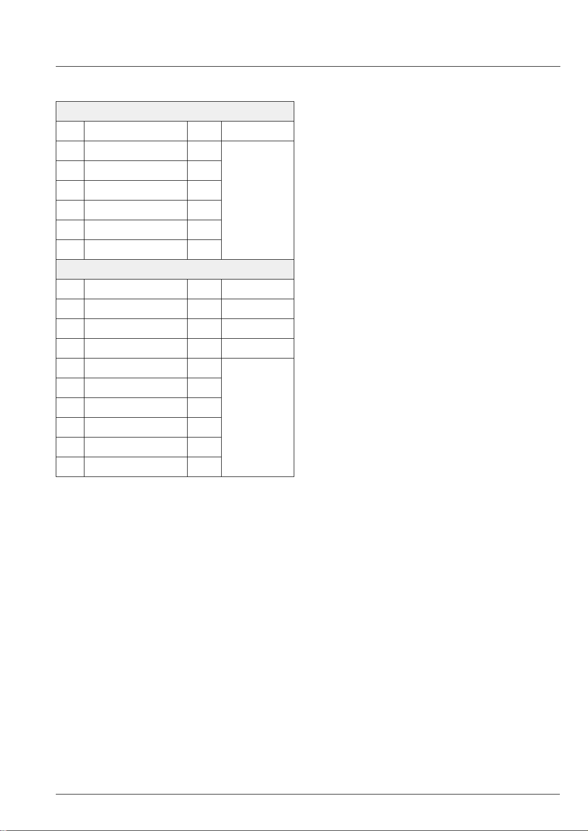
PRELIMINARY DATA SHEET MSP 34x1G
Table 6–12: Loading sequence for FIR-coefficients
FIR1 00 01
No. Symbol Name Bits Value
1 NICAM/FM2_Coeff. (5) 8
2 NICAM/FM2_Coeff. (4) 8
3 NICAM/FM2_Coeff. (3) 8
4 NICAM/FM2_Coeff. (2) 8
5 NICAM/FM2_Coeff. (1) 8
6 NICAM/FM2_Coeff. (0) 8
FIR2 00 05
No. Symbol Name Bits Value
1IMREG1 8 04
2IMREG1/IMREG2 8 40
3IMREG2 8 00
4 FM/AM_Coef (5) 8
5 FM/AM_Coef (4) 8
6 FM/AM_Coef (3) 8
7 FM/AM_Coef (2) 8
(MSP-Ch1: NICAM/FM2)
hex
(MSP-Ch2: FM1/AM)
hex
see Table 6–13
hex
hex
hex
see Table 6–13
The loading sequen ces must be obeyed. To change a
coefficient set, the complete block FIR1 or FIR2 must
be transmitted.
Note: For compatibility with MSP 3410B, IMREG1 and
IMREG2 have to be transmitted. The value for
IMREG1 and IMREG2 is 004. Due to the partitioning to
8-bit units, the val ues 04
hex
, 40
, and 00
hex
hex
arise.
6.3.7. DCO-Registers
Note: The use of this register is no longer recom-
mended. It should be us ed only in cases where software-compatibility to the MSP 34x0D is required.
Using the STANDARD SELECTION register together
with the MODUS register provides a more economic
way to program the MSP34x1G.
When selecting a TV-sound standard by means of the
STANDARD SELECT register, all frequency tuning is
performed automatically.
If manual setting of the tuning fr equency is requir ed, a
set of 24-bit reg isters determinin g the mixing freq uencies of the quadrature mix ers can be written manuall y
into the IC. In Table 6–14, some examples of DCO registers are listed. It is neces sary to divide them up into
low part and high part. The formul a for the calculation
of the registers for an y chosen IF frequency is as follows:
8 FM/AM_Coef (1) 8
9 FM/AM_Coef (0) 8
6.3.6. FIR-Parameter, Registers FIR1 and FIR2
Note: The use of this register is no longer recom-
mended. It should be used on ly in cases where software compatibility to the MSP 34x0D is required.
Using the STANDARD SELECTION register together
with the MODUS register provides a more economic
way to program the MSP 34x1G.
Data-shaping and/or FM/AM bandwidth limitation is
performed by a pair of linear phase Finite Impulse
Response filters (FIR-filter). The filter coefficients are
programmable and ar e either co nfigured autom aticall y
by the STANDARD SELECT register or written manually by the contr ol processor via the control bus. Two
not necessarily different sets of coefficients are
required: one for MSP- Ch1 (NICAM or FM2) and one
for MSP-Ch2 (FM1 = FM-mono). In Table 6–13 several
coefficient sets are proposed.
INCR
= int(f/fs ⋅ 224)
dec
with: int = integer function
f = IF frequency in MHz
= sampling frequency (18.432 MHz)
f
S
Conversion of INCR into he x-format a nd separation of
the 12-bit low and high parts lead to the required register values (DCO1_HI or _LO for MS P-Ch1, DCO2_HI
or LO for MSP-Ch2).
To load the FIR-filters, the following data val ues are to
be transferred 8 bits at a time embedded
LSB-bound in a 16-bit word.
MICRONAS INTERMETALL 91
Page 92
MSP 34x1G PRELIMINARY DATA SHEET
Table 6–13: 8-bit FIR-coefficients (decimal integer); reset status: all coefficients are “0”
Coefficients for FIR1 00 01
B/G-, D/K-
NICAM-FMI-NICAM-FML-NICAM-AM
Coef(i)
0
1
2
3
4
5
Mode-
FIR1 FIR2 FIR1 FIR2 FIR1 FIR2 FIR2 FIR2 FIR2 FIR2 FIR2 FIR2 FIR2 FIR2
2323−2
−
818 418−8
−
10 27
−
10 48
50 66 40 66 50 79 66 101 55 66 78 65 59 59
86 72 94 72 86 126 72 127 64 72 107 123 126 126
0 0 0 0 111111 0
REG[12]
Mode-
0 0 0 1 111111 0
REG[13]
and FIR2 00 05
hex
Terrestrial TV Standards
627−10
−
4 48 10 23 48 119 47 48 36 5 2 2
−
hex
FM - Satellite
FIR filter corresponds to a
band-pass with a bandwidth of B = 130 to 500 kHz
B/G-, D/K-,
M-Dual FM
4 3 7393−8
−
12 18 53 18 18
−
9 27 642827 4−16
−
130
kHz
180
kHz
200
kHz
280
kHz
B
frequency
f
c
380
500
kHz
kHz
1
−
8
−
−
1
−
9
1
−
8
−
Autosearch
1
−
1
−
8
−
For compatibility, except for the FIR2-AM and the Autosearch-sets, the FIR-filter programming as used for the MSP 3410B is also possible.
ADR coefficients are listed in the DRP data sheet.
Table 6–14: DCO registers for the MSP 34x1G; reset status: DCO_HI/LO = “0000”
DCO1_LO 00 93
Freq. MHz DCO_HI/hex DCO_LO/hex Freq. MHz DCO_HI/hex DCO_LO/hex
4.5 03E8 000
5.04
5.5
5.58
5.7421875
6.0
6.2
6.5
6.552
0460
04C6
04D8
04FC
0535
0561
05A4
05B0
7.02 0618 0000 7.2 0640 0000
7.38 0668 0000 7.56 0690 0000
, DCO1_HI 00 9B
hex
0000
038E
0000
00AA
0555
0C71
071C
0000
; DCO2_LO 00 A3
hex
5.76
5.85
5.94
6.6
6.65
6.8
, DCO2_HI 00 AB
hex
0500
0514
0528
05BA
05C5
05E7
hex
0000
0000
0000
0AAA
0C71
01C7
92 MICRONAS INTERMETALL
Page 93

PRELIMINARY DATA SHEET MSP 34x1G
6.4. Manual/Compatibility Mode: Description of Demodulator Read Registers
Note: The use of these register is no longer recom-
mended. It should be used on ly in cases where software compatibility to the MSP 34x0D is required.
Using the STANDARD SELECTION register together
with the STATUS reg ister provides a more economi c
way to program the MSP 34x1G and to retrie ve information from the IC.
All registers except C_AD_BITs are 8 bits wide. They
can be read out of the RAM of the MSP 34 x1G if the
MSP 34x0D Compatibility Mode is required.
All transmissions tak e place in 16- bit words. The v alid
8-bit data are the 8 LSBs of the received data word.
If the Automatic Sound Se lect feature is not used , the
NICAM or FM-identifi cation parameters must be re ad
and evaluated by the controller in order to enable
appropriate switching of the channel select matrix of
the baseband processing part. The FM-identification
registers are describ ed in section 6 .6.1. To handle t he
NICAM-sound and to observe the NICAM-quality, at
least the registers C_AD_BITS and ERROR_RATE
must be read and evaluated by the controller. Additional data bits and CIB bits, i f supplied by the NICA M
transmitter, can be obtained by reading the registers
ADD_BITS and CIB_BITS.
Table 6–15: NICAM operation modes as defined by
the EBU NICAM 728 specification
C4 C3 C2 C1 Operation Mode
0 0 0 0 Stereo sound (NICAMA/B),
independent mono sound (FM1)
0 0 0 1 Two independent mono signals
(NICAMA, FM1)
0 0 1 0 Three independent mono channels
(NICAMA, NICAMB, FM1)
0 0 1 1 Data transmission only; no audio
1 0 0 0 Stereo sound (NICAMA/B), FM1
carries same channel
1 0 0 1 One mono signal (NICAMA). FM1
carries same channel as NICAMA
1 0 1 0 Two independent mono channels
(NICAMA, NICAMB). FM1 carries
same channel as NICAMA
1 0 1 1 Data transmission only; no audio
x 1 x x Unimplemented sound coding
option (not yet defined by EBU
NICAM 728 specification)
AUTO_FM: monitor bit for the AUTO_FM Status:
0: NICAM sou r ce is NICAM
1: NICAM source is FM
6.4.1. NICAM Mode Control/Additional Data Bits Register
NICAM operation mode control bits and A[2:0] of the
additional data bits.
Format:
MSB C_AD_BITS 00 23
11...76543210
Auto
... A[2] A[1] A[0] C4 C3 C2 C1 S
_FM
hex
LSB
Important: “S” = Bit[0] indicates correct NICAM-syn-
chronization (S = 1). If S = 0, the MSP 3411/3451G
has not yet synchronized correctly to frame and
sequence, or has los t synchronization. T he remaining
read registers are ther efore not val id. The MSP m utes
the NICAM output automatic ally and tries to synchronize again as long as MODE_REG[6] is set.
The operation mod e is coded by C4-C1 as shown in
Table 6–15.
Note: It is no longer necessary to read out and evaluate the C_AD_BITS. All evaluation i s performe d in the
MSP and indicated in the STATUS register.
6.4.2. Additional Data Bits Register
Contains the remaining 8 of the 11 additional data bits.
The additional data bits are not yet defined by the
NICAM 728 system.
Format:
MSB ADD_BITS 00 38
76543210
A[10] A[9] A[8] A[7] A[6] A[5] A[4] A[3]
hex
LSB
6.4.3. CIB Bits Register
CIB bits 1 and 2 (see NICAM 728 specifications).
Format:
MSB CIB_BITS 00 3E
76543210
hex
LSB
xxxxxxCIB1CIB2
MICRONAS INTERMETALL 93
Page 94

MSP 34x1G PRELIMINARY DATA SHEET
6.4.4. NICAM Error Rate Register
ERROR_RATE 00 57
Error free 0000
maximum error rate 07FF
hex
hex
hex
Average error rate of the NICAM reception in a time
interval of 182 ms, whi ch shou ld be clo se to 0. The in itial and maximum value of ERROR_RATE is 2047.
This value is also active if the NICAM bit of
MODE_REG is not set. S inc e t he v alue i s ac hie ve d by
filtering, a certain transition time (approx. 0.5 sec) is
unavoidable. Acceptable audio may have error rates
up to a value of 700 int. Individual evaluation of this
value by the controller and an appropriate threshold
may define the fallback mode from NICAM to
FM/AM-Mono in case of poor NICAM reception.
The bit error rate per s econd (B ER) ca n be ca lculated
by means of the following formula:
6
−
BER = ERROR_RATE * 12.3*10
/s
6.4.5. PLL_CAPS Readback Register
It is possible to read out the actual setting of the
PLL_CAPS. In standard applications, this register is
not of interest for the customer.
PLL_CAPS 02 1F
hex
L
6.4.7. Automatic Search Function for FM-Carrier
Detection in Satellite Mode
The AM demodulat ion abil ity of t he MSP 3 4x1G o ffers
the possibility to calculate the “field strength” of the
momentarily selected FM carrier, which can be read
out by the controll er. In SAT receivers, this feature can
be used to make auto matic FM carrier search possible.
For this, the MSP has to be switched to AM-mode
(MODE_REG[8]), FM-Prescale must be set to
7F
hex
=+127
, and the FM DC notch (see section
dec
6.5.7.) must be switched off. The sound-IF freque ncy
range must now be “sc anned” in the MSP-channel 2
by means of the programma ble quadrature mixer wi th
an appropriate incremental frequency (i.e. 10 kHz).
After each incrementation, a field strength value is
available at the quasi-peak detector output (quasipeak detector source must be set to FM), which must
be examined for relative maxima by the controller. This
results in either continuing search or switching the
MSP back to FM demodulation mode.
During the search proces s, the FIR2 must be loaded
with the coefficient set “AUTOSEARCH”, which
enables small b andwidth, resu lting in a ppropriate f ield
strength characteristics. The absolute field strength
value (can be read out of “quasi-peak detector output
FM1”) also gives information on whether a main FM
carrier or a subcarrier was detected; and as a practical
consequence, the FM bandwidth (FIR1/2) and the
deemphasis (50 µs or adaptive) can be switched
accordingly.
minimum frequency 1111 1111 FF
nominal frequency 0101 0110 56
RESET
maximum frequency 0000 0000 00
PLL_CAPS 02 1F
PLL open xxxx xxx0
PLL closed xxxx xxx1
hex
H
hex
hex
hex
6.4.6. AGC_GAIN Readback Register
It is possible to read out the actual setting of
AGC_GAIN in Automatic Gain Mode. In standard
applications, this regi ster is not of interest for the customer.
AGC_GAIN 02 1E
max. amplification
(20 dB)
min. amplification
(3 dB)
hex
0001 0100 14
0000 0000 00
hex
hex
Due to the fact that a constant demodulation frequency
offset of a few kHz leads to a DC level in the d emodulated signal, furthe r fin e tuni ng of th e f ound c ar rie r c an
be achieved by evaluating the “DC Level Readout
FM1”. Therefore, the FM DC Notch must be switched
on, and the demodulator part must be switched back to
FM-demodulation mode.
For a detailed description of the automatic search
function, please refer to the correspondin g MSP Windows software.
94 MICRONAS INTERMETALL
Page 95

PRELIMINARY DATA SHEET MSP 34x1G
6.5. Manual/Compatibility Mode: Description of DSP Write Registers
6.5.1. Additional Channel Matrix Modes
Loudspeaker Matrix 00 08
Headphone Matrix 00 09
SCART1 Matrix 00 0A
SCART2 Matrix 00 41
I2S Matrix 00 0B
Quasi-Peak
Detector Matrix
00 0C
hex
hex
hex
hex
hex
hex
SUM/DIFF 0100 0000 40
AB_XCHANGE 0101 0000 50
PHASE_CHANGE_B 0110 0000 60
PHASE_CHANGE_A 0111 0000 70
A_ONLY 1000 0000 80
L
L
L
L
L
L
hex
hex
hex
hex
hex
6.5.2. Volume Modes of SCART1/2 Outputs
Volume Mode SCART1 00 07
Volume Mode SCART2 00 40
linear 0000 0
logarithmic 0001 1
Linear Mode
Volume SCART1 00 07
Volume SCART2 00 40
OFF 0000 0000 00
0dB gain
(digital full scale (FS) to 2
output)
V
RMS
+6 dB gain (−6 dBFS to 2
output)
V
RMS
hex
hex
RESET
hex
hex
RESET
0100 0000 40
0111 1111 7F
[3:0]
[3:0]
hex
hex
H
H
hex
hex
hex
B_ONLY 1001 0000 90
hex
This table shows additional modes for the channel
matrix registers.
The sum/difference mode can be used together with
the quasi-peak detec tor to determine the sound material mode. If the difference signal on ch annel B (right)
is near to zero, and the sum signa l on channel A (left)
is high, the incoming audi o s ig nal is mon o. If th er e is a
significant level on the difference sig nal, the incoming
audio is stereo.
Note: SCART Volume linear mode will not be supported in the future ( documented for c ompatibilit y reasons only).
6.5.3. FM Fixed Deemphasis
FM Deemphasis 00 0F
hex
50 µs 0000 0000 00
RESET
75 µs 0000 0001 01
OFF 0011 1111 3F
H
hex
hex
hex
6.5.4. FM Adaptive Deemphasis
FM Adaptive
Deemphasis WP1
OFF 0000 0000 00
00 0F
RESET
hex
L
hex
WP1 0011 1111 3F
hex
6.5.5. NICAM Deemphasis
A J17 Deemphasis is always applied to the NICAM
signal. It is not switchable.
MICRONAS INTERMETALL 95
Page 96

MSP 34x1G PRELIMINARY DATA SHEET
6.5.6. Identification Mode for A2 Stereo Systems
Identification Mode 00 15
Standard B/G
(German Stereo)
Standard M
(Korean Stereo)
Reset of Ident-Filter 0011 1111 3F
hex
0000 0000 00
RESET
0000 0001 01
L
hex
hex
hex
To shorte n the r espon se time of the identific at ion al gorithm after a program chan ge between two FM- Stereo
capable programs, th e reset of the ident-filter can be
applied.
Sequence:
1. Program change
2. Reset ident-filter
3. Set identification mode back to standard B/G or M
4. Read stereo detection register
6.5.7. FM DC Notch
The DC compensation filter (FM DC Notch) for FM
input can be switched off. This is used to speed up the
automatic search functio n (see Section 6.4.7.) . In normal FM-mode, the FM DC Notch should be switche d
on.
6.6.1. Stereo Detection Register for A2 Stereo Systems
Stereo Detection
Register
Stereo Mode Reading
MONO near zero
STEREO positive value (ideal
BILINGUAL negative value (ideal
00 18
hex
(two’s complement)
reception: 7F
reception: 80
hex
hex)
)
H
Note: It is no longer necessar y to read out and evalu-
ate the A2 identification level. All evaluation is performed in the MSP and indicated in the STATUS register.
6.6.2. DC Level Register
DC Level Readout
FM1 (MSP-Ch2)
DC Level Readout
FM2 (MSP-Ch1)
DC Level [8000
00 1B
hex
00 1C
hex
... 7FFF
hex
values are 16 bit two’s
complement
H+L
H+L
hex
]
FM DC Notch 00 17
ON 0000 0000 00
OFF 0011 1111 3F
hex
Reset
L
hex
hex
6.6. Manual/Compatibility Mode: Description of DSP Read Registers
All readable registers are 16-bit wide. Transmissions
2
C bus have to ta ke plac e in 16 -bi t wo rds. Some of
via I
the defined 16-bit words ar e divided i nto low an d high
byte, thus holding two different control entities.
These registers are not writable.
The DC level re gister me asures th e DC comp onent of
the incoming FM sign als (FM1 and FM2). This can be
used for seek function s in sat ellite receiv ers and for IF
FM frequencies fine tuning. A too low demodulation
frequency (DCO) results in a positive DC-level and
vice versa. For furthe r processing, the DC content of
the demodulated FM signals is suppressed. Th e time
constant τ, defining the tra nsition time o f the D C Le vel
Register, is approximately 28 ms.
6.7. Demodulator Source Channels in Manual Mode
6.7.1. Terrestric Sound Standards
Table 6–16 sh ows the source channel assignment of
the demodulated sig nals in case of manual mode for
all terrestric sound standards. See Table 2–2 for the
assignment in the Automatic Sound Select mode. In
manual mode for terres tric sound standards, only two
demodulator sources are defined.
6.7.2. SAT Sound Standards
Table 6–17 sh ows the source channel assignment of
the demodulated signals for SAT sound standards.
96 MICRONAS INTERMETALL
Page 97

PRELIMINARY DATA SHEET MSP 34x1G
Table 6–16: Manual Sound Select Mode for Terrestric Sound Standards
Source Channels of Sound Select Block
Broadcasted
Sound
Standard
B/G-FM
D/K-FM
M-Korea
M-Japan
B/G-NICAM
L-NICAM
I-NICAM
D/K-NICAM
D/K-NICAM
(with high
deviation FM)
BTSC
Selected MSP
Standard
Code
03
04, 05
02
30
08
09
0A
0B
0C
20
21
Broadcasted
Sound Mode
FM Matrix FM/AM
(use 0 for channel select)
Stereo or A/B
(use 1 for channel select)
MONO Sound A Mono Mono Mono
STEREO German Stereo
Stereo Stereo
Korean Stereo
BILINGUAL,
Languages A and B
NICAM not available
or NICAM error rate
too high
No Matrix Left = A
Right = B
Left = A
Right = B
Sound A Mono analog Mono no sound
with AUTO_FM:
analog Mono
MONO Sound A Mono analog Mono NICAM Mono
STEREO Sound A Mono analog Mono NICAM Stereo
BILINGUAL,
Languages A and B
Sound A Mono analog Mono Left = NICAM A
Right = NICAM B
MONO Sound A Mono Mono Mono
STEREO Korean Stereo Stereo Stereo
MONO + SAP Soun d A Mono Mono Mono
STEREO + SAP Korean Stereo Stereo Stereo
MONO
Sound A Mono Mono Mono
STEREO
MONO + SAP
STEREO + SAP
No Matrix
Left = Mono
Right = SAP
Left = Mono
Right = SAP
FM-Radio 40
MONO Sound A Mono Mono Mono
STEREO Korean Stereo Stereo Stereo
T able 6–17: Manual Sound Select Modes for SAT-Modes (FM Matrix is set automatically)
Source Channels of Sound Select Block for SAT- Mo des
Broadcasted
Sound
Standard
FM SAT
Selected
MSP Standar d
Code
6, 50
hex
51
hex
Broadcasted
Sound Mode
MONO Mono Mono Mono Mono
STEREO Stereo Stereo Stereo Stereo
BILINGUAL Left = A (FM1)
FM/AM
(source select: 0)
Right = B (FM2)
Stereo or A/B
(source select: 1)
Left = A (FM1)
Right = B (FM2 )
Stereo or A
(source select: 3)
A (FM1) B (FM2)
Stereo or B
(source select: 4)
MICRONAS INTERMETALL 97
Page 98

MSP 34x1G PRELIMINARY DATA SHEET
6.8. Exclusions of Audio Baseband Features
In general, all functions can be switched independently.
Two exceptions exist:
1. NICAM cannot be processed simultaneously with
the FM2 channel.
2. FM adaptive deemphasis cannot be processed
simultaneously with FM-identification.
6.9. Phase Relationship of Analog Outputs
The analog output si gnals: Loudspeaker, headphone,
and SCART2 all have the same phases. The user
does not need to correct output phases when using
these analog outputs directly. The SCART1 output has
opposite phase.
2
Using the I
ers, care must be taken to adjust for the correct phase.
If the attached coprocesso r is one of the MSP family,
the following schem atics help to determine the phase
relationship.
S-outputs for other DSPs or D/A convert-
SCART1
SCART2
SCART3
SCART4
MONO
SCART
DSP
Input
Select
I2S_OUT1/2I2S_IN1/2
Audio
Baseband
Processing
MONO, SCART1...4
SCART1-Ch.
SCART2-Ch.
Loudspeaker
Headphone
SCART1
SCART2
SCART
Output Select
Fig. 6–2: Phase diagram of the MSP 34x1G
98 MICRONAS INTERMETALL
Page 99

PRELIMINARY DATA SHEET MSP 34x1G
7. Appendix D: MSP 34x1G Version History
MSP 3451G-A1
First release
MSP 3451G-A2
– CONTROL register now readable for more status
information
– new D/K standard for Poland
2
– improved I
C hardware problem handling
– improved AM-performance
MICRONAS INTERMETALL 99
Page 100

MSP 34x1G PRELIMINARY DATA SHEET
8. Appendix E: Application Circuit
5V
DVSS
AHVSS
AHVSS
AHVSS
5V
DVSS
Tuner 2
Tuner 1
330 nF
330 nF
330 nF
330 nF
330 nF
330 nF
330 nF
330 nF
330 nF
IF 2 IN
Signal GND
IF 1 IN
56 pF 56 pF 56 pF
ANA_IN1+ (58) 25
28 (55) MONO_IN
31 (52) SC1_IN_L
30 (53) SC1_IN_R
32 (51) ASG1
34 (49) SC2_IN_L
33 (50) SC2_IN_R
35 (48) ASG2
37 (46) SC3_IN_L
36 (47) SC3_IN_R
38 (45) ASG4
40 (43) SC4_IN_L
39 (44) SC4_IN_R
11 (7) STANDBYQ
12 (6) ADR_SEL
8 (10) I2C_DA
9 (9) I2C_CL
1 (16) ADR_WS
68 (17) ADR_CL
3 (15) ADR_DA
6 (12) I2S _WS
7 (11) I2S _CL
4 (14) I2S _DA_IN1
65 (20) I2S_DA_IN2
5 (13) I2S _DA_OUT
100
10
-
nF
µF
+
3.3 µF100
+
ANA_IN− (59) 24
ANA_IN2+ (60) 23
VREFTOP (54) 29
MSP 34x1G
if ANA_IN2+ not used
C s. section 4.6.2.
18.432
MHz
nF
10 µF10 µF
AGNDC (42) 42
XTAL_IN (62) 21
XTAL_OUT (63) 20
DACM_SUB (31) 54
SC1_OUT_L (37) 47
SC1_OUT_R (36) 48
SC2_OUT_L (34) 50
SC2_OUT_R (33) 51
D_CTR_I/O_0 (5) 13
D_CTR_I/O_1 (4) 14
AUD_CL_OUT (1) 18
8V(5V)
++
CAPL_A (38) 46
CAPL_M (40) 44
DACM_L (29) 56
DACM_R (28) 57
DACA_L (26) 59
DACA_R (25) 60
TESTEN (61) 22
1 nF
1 nF
1 nF
1 nF
1 nF
100
100
100
100
100 pF 56 pF
1 µF
1 µF
1 µF
1 µF
1 µF
Ω
22 µF
+
Ω
22 µF
+
Ω
22 µF
+
Ω
22 µF
+
AHVSS
ANA_IN1+
Alternative circuit for
1 KΩ
ANA_IN1+for more
attenuation of video
components:
LOUD
SPEAKER
HEAD
PHONE
45 (39) AHVSUP
470
pF
1.5
nF
10
µF
43 (41) AHVSS
49 (35) VREF1
58 (27) VREF2
Note: Pin numbers refer to the
PLCC68 package, numbers in
brackets refer to the PSDIP64
package.
RESETQ
(from Controller, see section 4.6.3.3.)
61 (24) RESETQ
220
pF
470
pF
1.5
nF
10
µF
67 (18) DVSUP
26 (57) AVSUP
66 (19) DVSS
470
pF
1.5
nF
10
µF
27 (56) AVSS
5 V 5 V 8 V
AVSS
(5 V)
AHVSS
AHVSS
AHVSS
100 MICRONAS INTERMETALL
 Loading...