

Page 1
19" LCD Color Monitor Chassis: HUDSON 9
Service
Service
Service
190V9FB/97(1)
190V9FB/27(1)
190V9FB/05(1)
190V9FB/00(1)
190V9FB/62(1)
190V9FB/93(1)
190V9FB/94(1)
190V9FB/93(2)
190V9FB/94(2)
Description Page Description Page
Table Of Contents........................................………….1
Page
Revision List................................................…………….2
Important Safety Notice………….................................3
1. Monitor Specifications……...................................…..4
2. LCD Monitor Description………..…….........................5
3. Operation instructions…………….......................…....6
3.1General Instructions…………………..…..…………6
3.2 Control buttons…………..……………………………6
3.3 Adjusting the Picture……....................................…..8
3.4 Connecting to the PC ….........…….…........……....10
4. Input/Output Specification.........................………….11
4.1 Input Signal Connector...........................…………..11
4.2 Factory Preset Display Modes...............................11
4.3 Pixel Defect Policy……………………………………12
4.4 Failure Mode Of Panel ………………………………15
5. Block Diagram……………………………................16
5.1 Software Flow Chart............................………….....16
5.2 Electrical Block Diagram..................……….........18
6. Schematic Diagram…….....................……….........20
6.1 Main Board…….……………..….……………………20
6.2 Power Board…………………………..…………………25
6.3 Key Board…….………………………..…………………27
7. PCB Layout.....……......................……………………..28
7.1 Main Board.....…….......................……..…………......28
7.2 Power Board.……................…..…………….............30
7.3 Key Board………...………………………………………32
8. Wiring Diagram……………………………………….…..33
9. Scalar Board Overview…………....………………….…..34
10. Mechanical Instructions.....……...…………..…..........35
11.Trouble shooting…..…………………………...……..39
12. Repair Flow Chart…….…….……………………………41
13. ISP Instructions..…..........................………..............47
14. DDC Instructions……......…….............….................55
15. White Balance, Luminance Adjustment……............63
16. Monitor Exploded View………..…….………..............65
17. Recommended & Spare Parts List...……...................66
18. Different Parts List...…………………….…...................68
19. General Product Specification………………….……….71
http://www.wjel.net
ANY PERSON ATTEMPTING TO SERVICE THIS CHASSIS MUST FAMILIARIZE HIMSELF WITH THE
CHASSIS AND BE AWARE OF THE NECESSARY SAFETY PRECAUTIONS TO BE USED WHEN
SERVICING ELECTRONIC EQUIPMENT CONTAINING HIGH VOLTAGES.
CAUTION: USE A SEPARATE ISOLATION TRANSFOMER FOR THIS UNIT WHEN SERVICING
SAFETY NOTICE
REFER TO BACK COVER FOR IMPORTANT SAFETY GUIDELINES
Copyright 2008 Philips Consumer Lifestyle Subject to modification ○K Apr, 02, 2008
GB
3122 785 17850
Page 2
2
HUDSON 9
Revision List
Version Release Date Revision History
A00 Apr.02, 2008 Initial release, Draft Version
Add CTV Model 190V9FB/27, 190V9FB05 and 190V9FB/00
A01 Apr.10, 2008
Add CTV Model 190V9FB/97 and it’s Philips 12NC
A02 Apr.17, 2008 Add two new panels for 190V9FB/97
A03 Apr.30, 2008
A03 May.15, 2008
A04 Aug.10.2008
Add CTV Model 190V9FB/93 and 190V9FB/94
Perfect Philips 12NC for 190V9FB/93 and 190V9FB/94
Add panel for 190V9FB/93
http://www.wjel.net
Page 3

HUDSON 9
3
Important Safety Notice
Proper service and repair is important to the safe, reliable operation of all Philips Company Equipment. The service
procedures recommended by Philips and described in this service manual are effective methods of performing
service operations. Some of these service operations require the use of tools specially designed for the purpose.
The special tools should be used when and as recommended.
It is important to note that this manual contains various CAUTIONS and NOTICES which should be carefully read
in order to minimize the risk of personal injury to service personnel. The possibility exists that improper service
methods may damage the equipment. It is also important to understand that these CAUTIONS and NOTICES ARE
NOT EXHAUSTIVE. Philips could not possibly know, evaluate and advise the service trade of all conceivable ways
in which service might be done or of the possible hazardous consequences of each way. Consequently, Philips has
not undertaken any such broad evaluation. Accordingly, a servicer who uses a service procedure or tool which is
not recommended by Philips must first satisfy himself thoroughly that neither his safety nor the safe operation of
the equipment will be jeopardized by the service method selected.
Hereafter throughout this manual, Philips Company will be referred to as Philips.
WARNING
Use of substitute replacement parts, which do not have the same, specified safety characteristics may create
shock, fire, or other hazards.
Under no circumstances should the original design be modified or altered without written permission from Philips.
Philips assumes no liability, express or implied, arising out of any unauthorized modification of design.
Servicer assumes all liability.
FOR PRODUCTS CONTAINING LASER:
DANGER-Invisible laser radiation when open. AVOID DIRECT EXPOSURE TO BEAM.
CAUTION-Use of controls or adjustments or performance of procedures other than those specified herein may
result in hazardous radiation exposure.
CAUTION -The use of optical instruments with this product will increase eye hazard.
TO ENSURE THE CONTINUED RELIABILITY OF THIS PRODUCT, USE ONLY ORIGINAL MANUFACTURER'S
REPLACEMENT PARTS, WHICH ARE LISTED WITH THEIR PART NUMBERS IN THE PARTS LIST SECTION
OF THIS SERVICE MANUAL.
Take care during handling the LCD module with backlight unit
-Must mount the module using mounting holes arranged in four corners.
-Do not press on the panel, edge of the frame strongly or electric shock as this will result in damage to the screen.
-Do not scratch or press on the panel with any sharp objects, such as pencil or pen as this may result in damage to
the panel.
-Protect the module from the ESD as it may damage the electronic circuit (C-MOS).
-Make certain that treatment person’s body is grounded through wristband.
-Do not leave the module in high temperature and in areas of high humidity for a long time.
-Avoid contact with water as it may a short circuit within the module.
-If the surface of panel becomes dirty, please wipe it off with a soft material. (Cleaning with a dirty or rough cloth
http://www.wjel.net
may damage the panel.)
Page 4
4
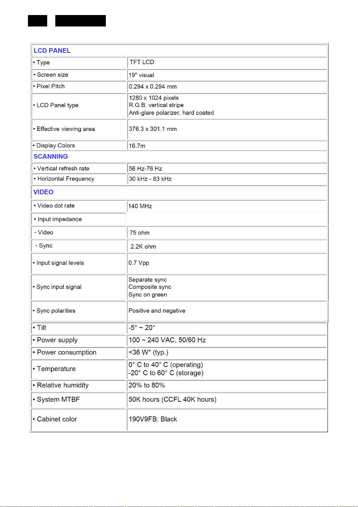
1. Monitor Specifications
HUDSON 9
http://www.wjel.net
Page 5
(
HUDSON 9
5
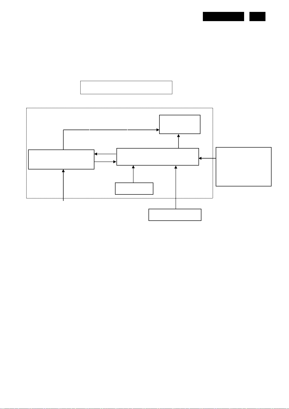
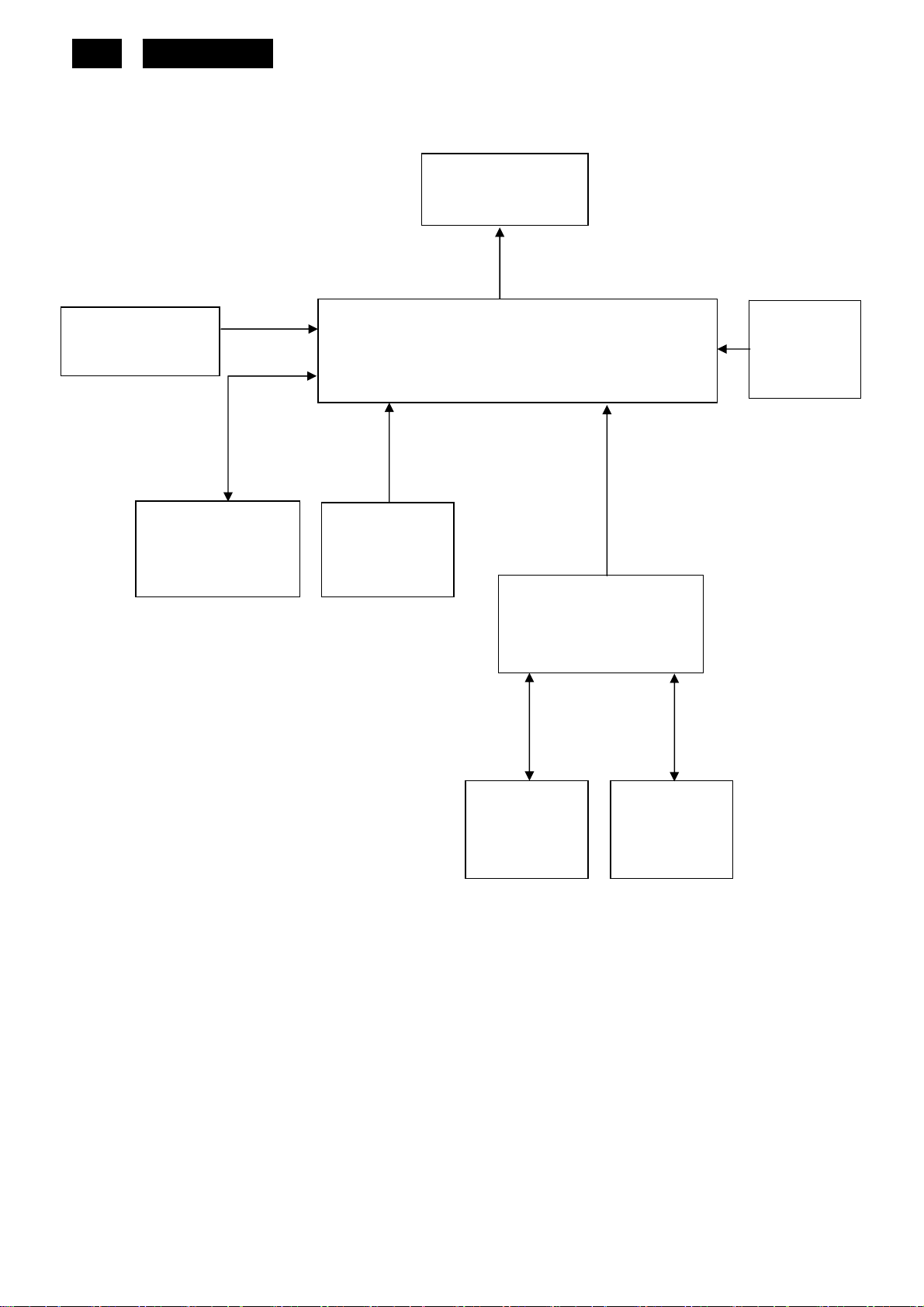
2. LCD Monitor Description
The LCD monitor will contain a main board, a power board and a key board which house the flat panel control logic,
brightness control logic and DDC.
The power board will provide AC to DC Inverter voltage to drive the backlight of panel and the main board chips
each voltage.
Power board
Include: adapter, inverter)
AC-IN
100V-240V
Monitor Block Diagram
CCFL Drive.
Key Board
Flat Panel and
CCFL backlight
Main Board
HOST Computer
RS232 Connector
For white balance
adjustment in factory
mode
Video signal, DDC
http://www.wjel.net
Page 6
6
HUDSON 9
3. Operating Instructions
3.1 General Instructions
Press the power button to turn the monitor on or off. The other control buttons are located at the front of the
panel of the monitor.
By changing these settings, the picture can be adjusted to your personal preferences.
The power cord should be connected.
-
Connect the video cable from the monitor to the video card.
-
Press the power button to turn on the monitor, the power indicator will light up.
-
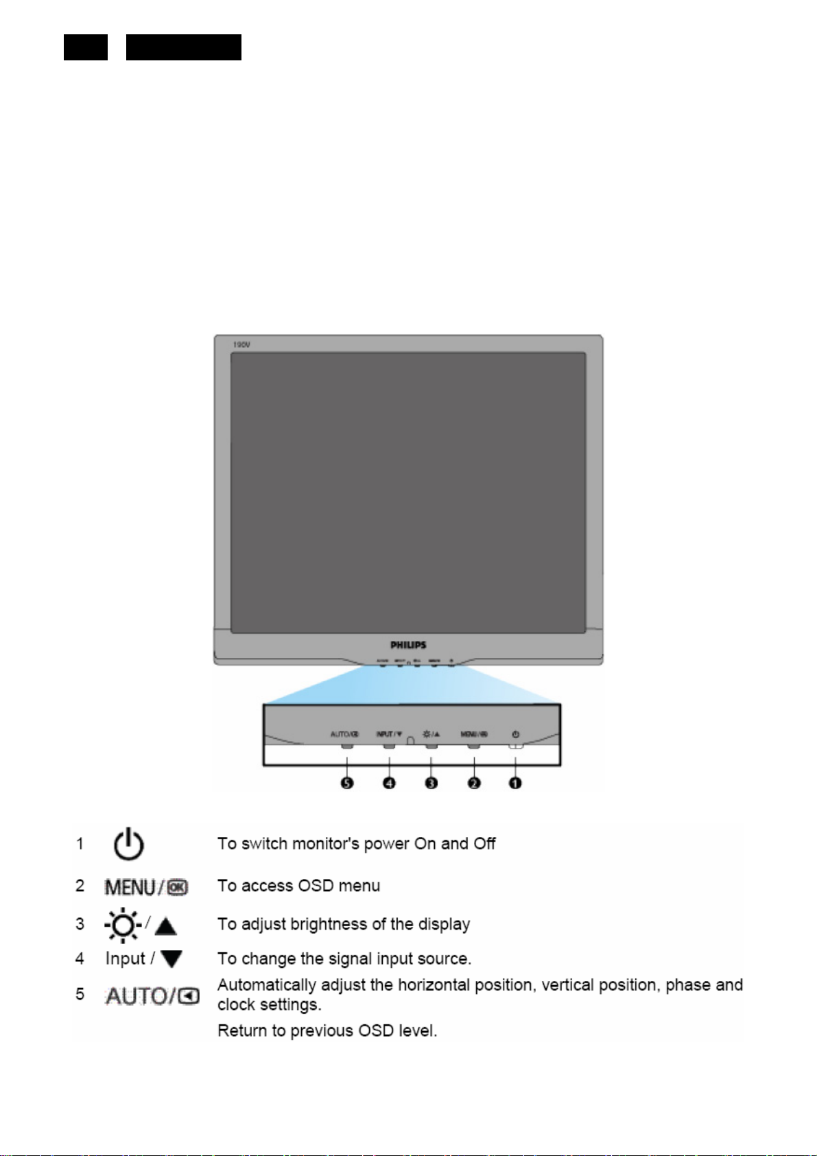
3.2 Control Buttons
Front View
http://www.wjel.net
Page 7
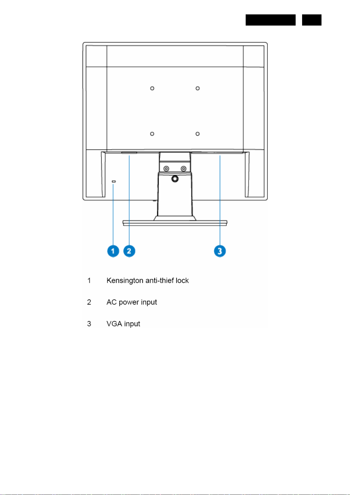
Rear View
HUDSON 9
7
http://www.wjel.net
Page 8
8
3.3 Adjusting the Picture
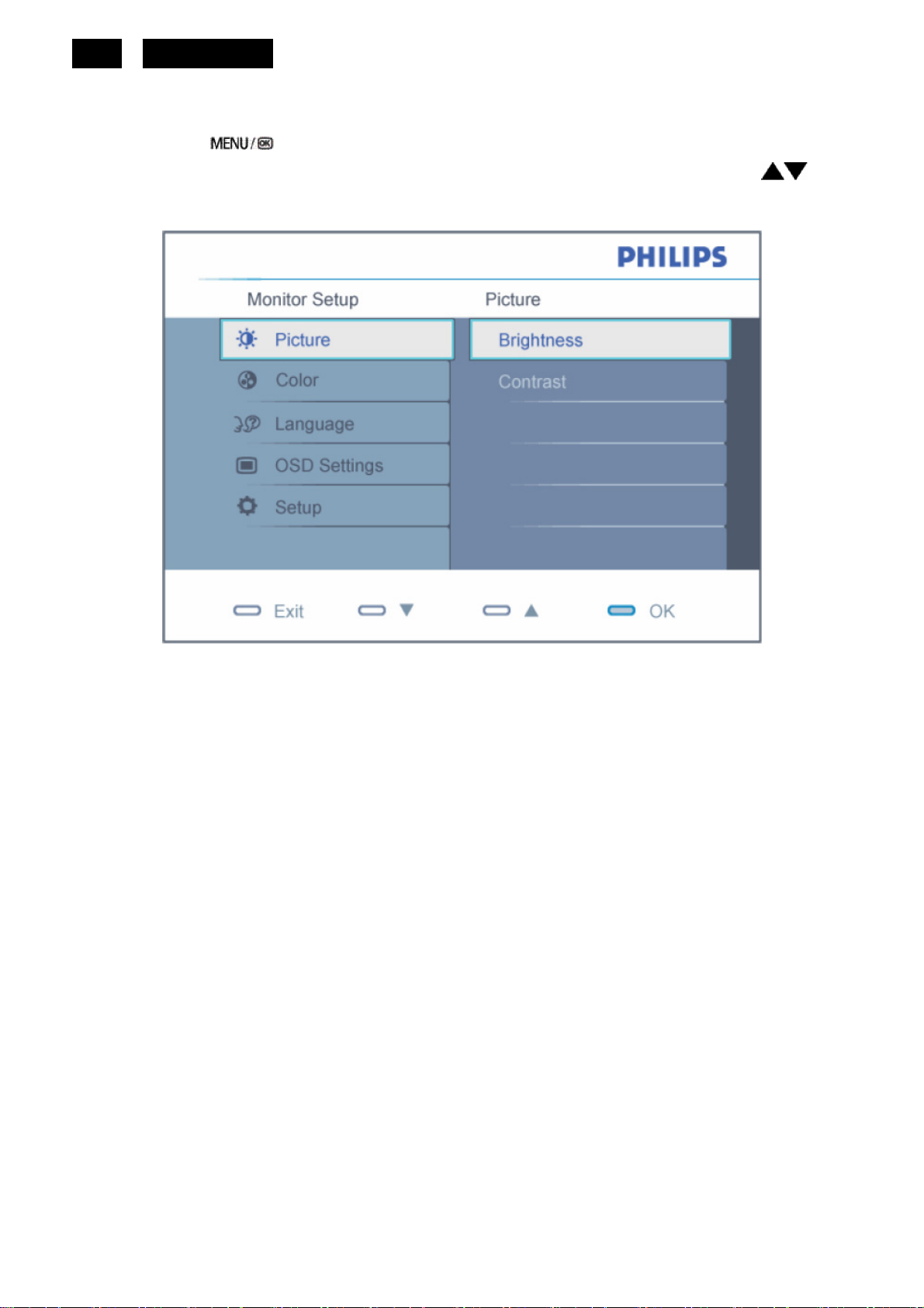
Description of the On Screen Display
When you press the button on the front control of your monitor, the On-Screen Display (OSD) Main Controls
HUDSON 9
window will pop up and you can then start making adjustments to your monitor's various features. Use the
make your adjustments.
keys to
To Lock/Unlock OSD function (User Mode)
The OSD function can be locked by pressing “MENU” button for more than 10 seconds.
Locked OSD function can be released by pressing “MENU” button for more than 10 seconds again.
http://www.wjel.net
Page 9
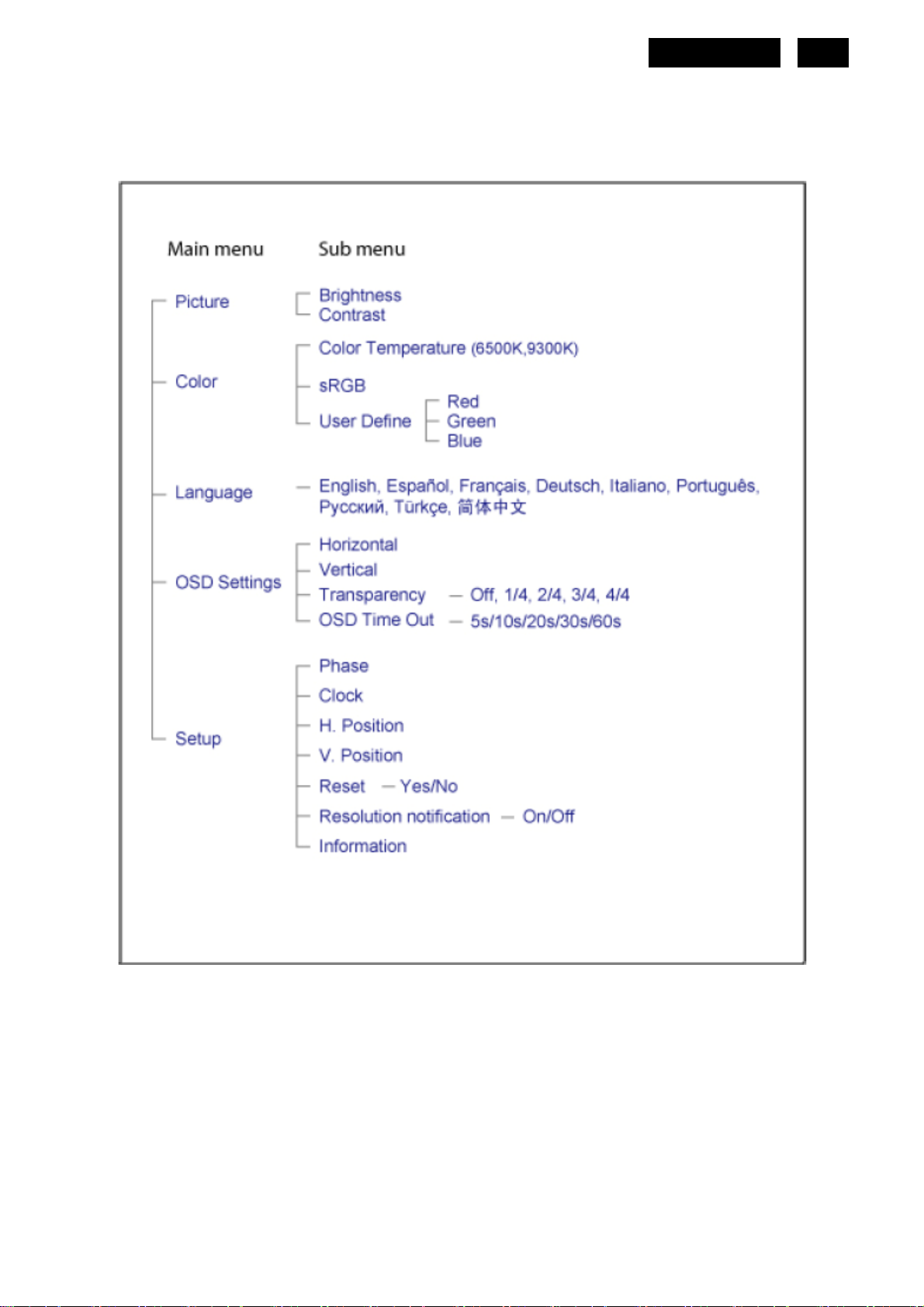
The OSD Tree
Below is an overall view of the structure of the On-Screen Display. You can use this as a reference when you want
to work your way around the different adjustments later on.
HUDSON 9
9
http://www.wjel.net
Page 10
10
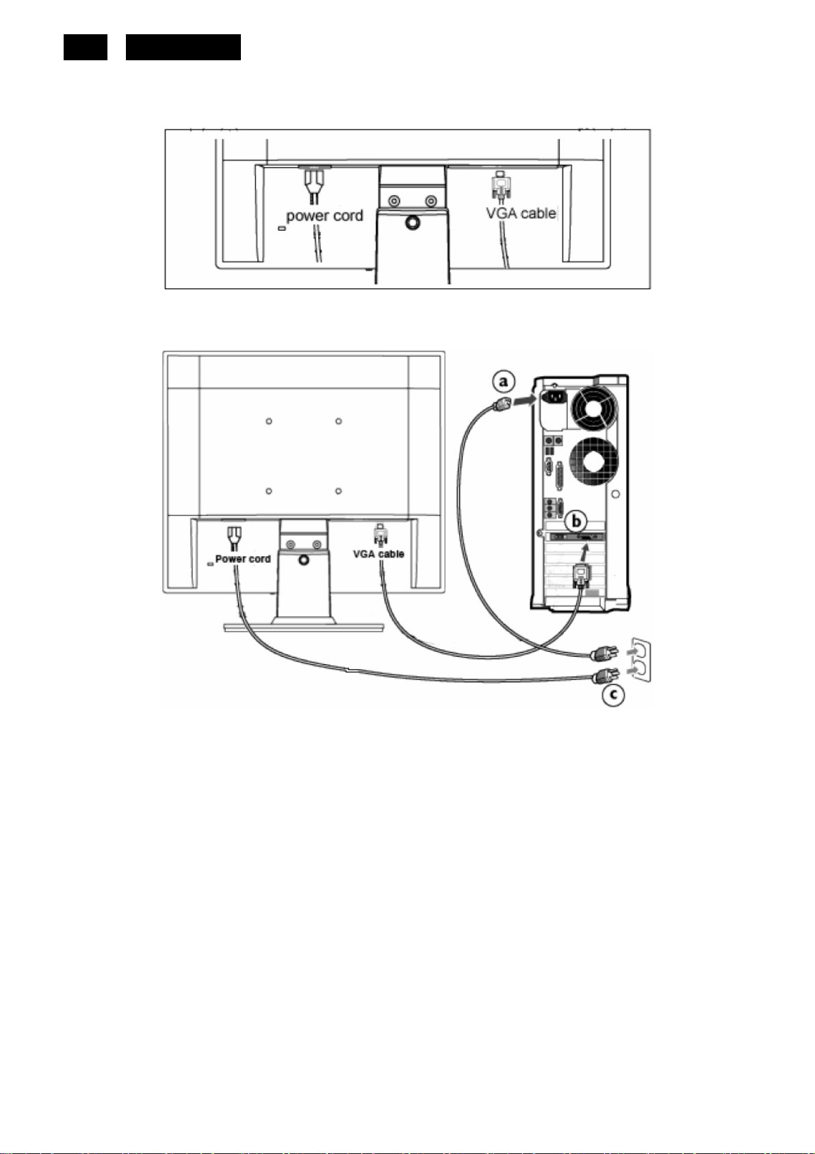
3.4 Connecting to the PC
1) Connect the power cord to the back of the monitor firmly.
HUDSON 9
2) Connect to PC
(a) Turn off your computer and unplug its power cable.
(b) Connect the monitor signal cable to the video connector on the back of your computer.
(c) Plug the power cord of your computer and your monitor into a nearby outlet.
http://www.wjel.net
(d) Turn on your computer and monitor. If the monitor displays an image, installation is complete.
Page 11
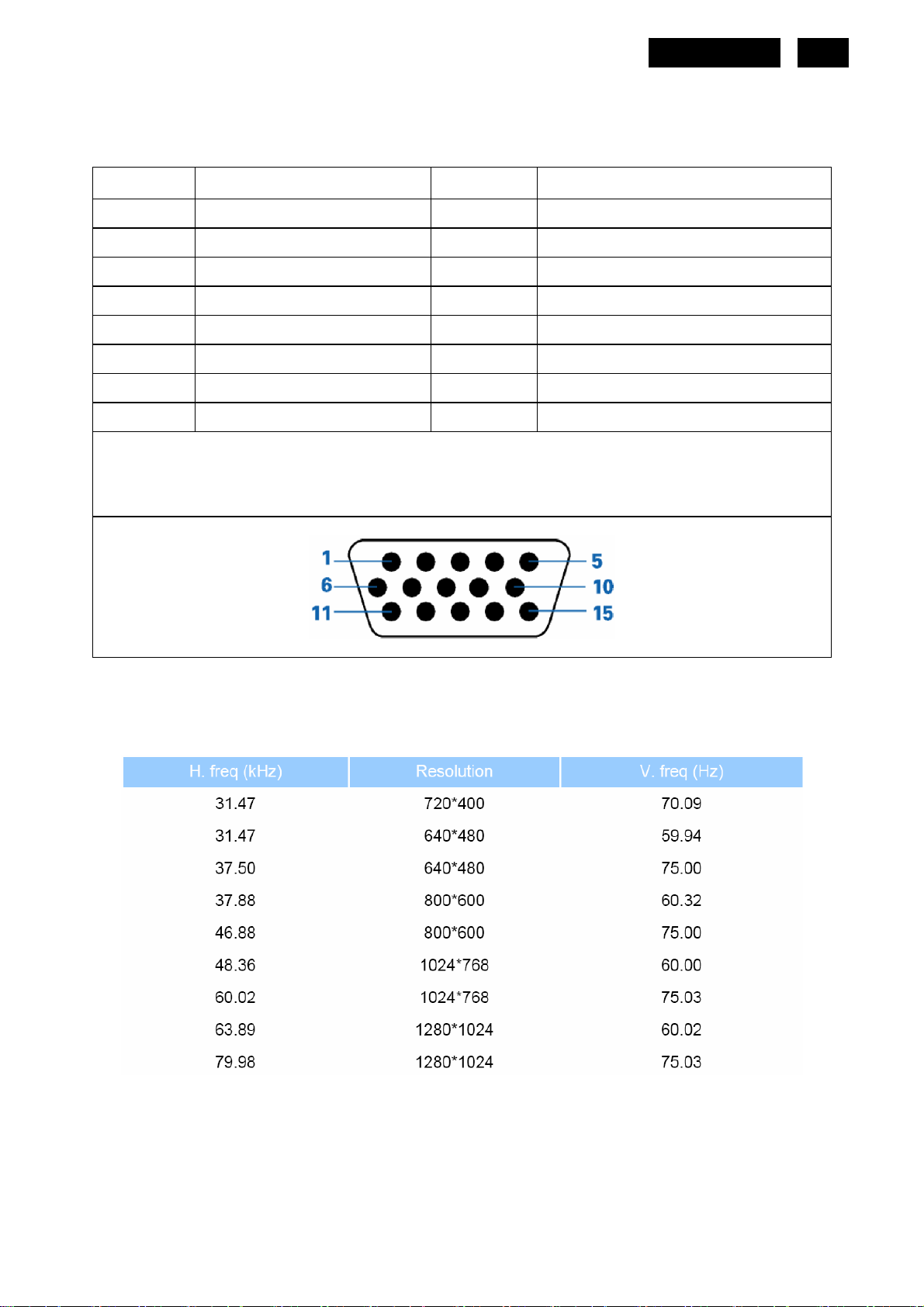
4. Input/ Output Specification
4.1 Input Signal Connector
Analog connectors
Pin No. Description Pin No. Description
1. Red video input 9. DDC +5V
2. Green video input 10. Logic Ground
3. Blue video input 11. Ground
4. Sense (GND) 12. Serial data line (SDA)
5. Cable detect (GND) 13. H. Sync/ H+ V. Sync
6. Red video ground 14. V. Sync
7. Green video ground 15. Data clock line (SCL)
8. Blue video ground
VGA connector layout
HUDSON 9
11
4.2 Factory Preset Display Modes
http://www.wjel.net
Page 12
12
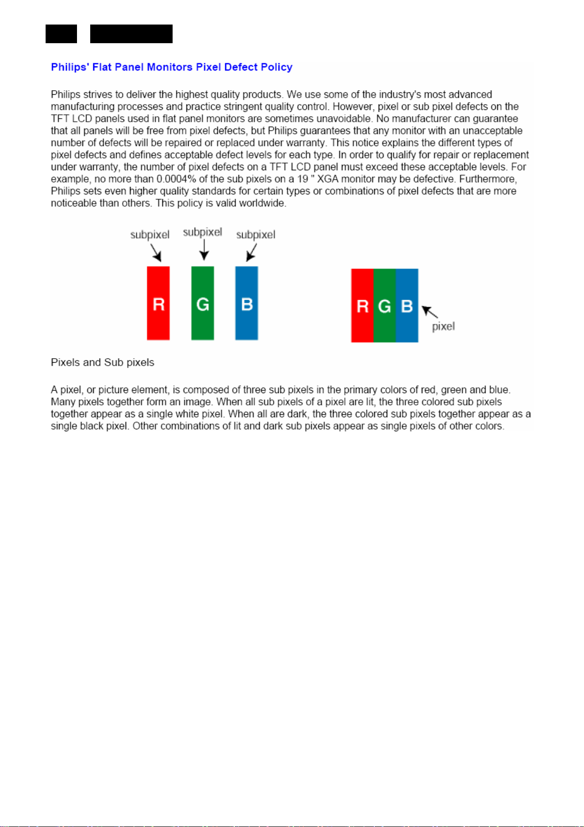
4.3 Pixel Defect Policy
HUDSON 9
http://www.wjel.net
Page 13
HUDSON 9
13
http://www.wjel.net
Page 14
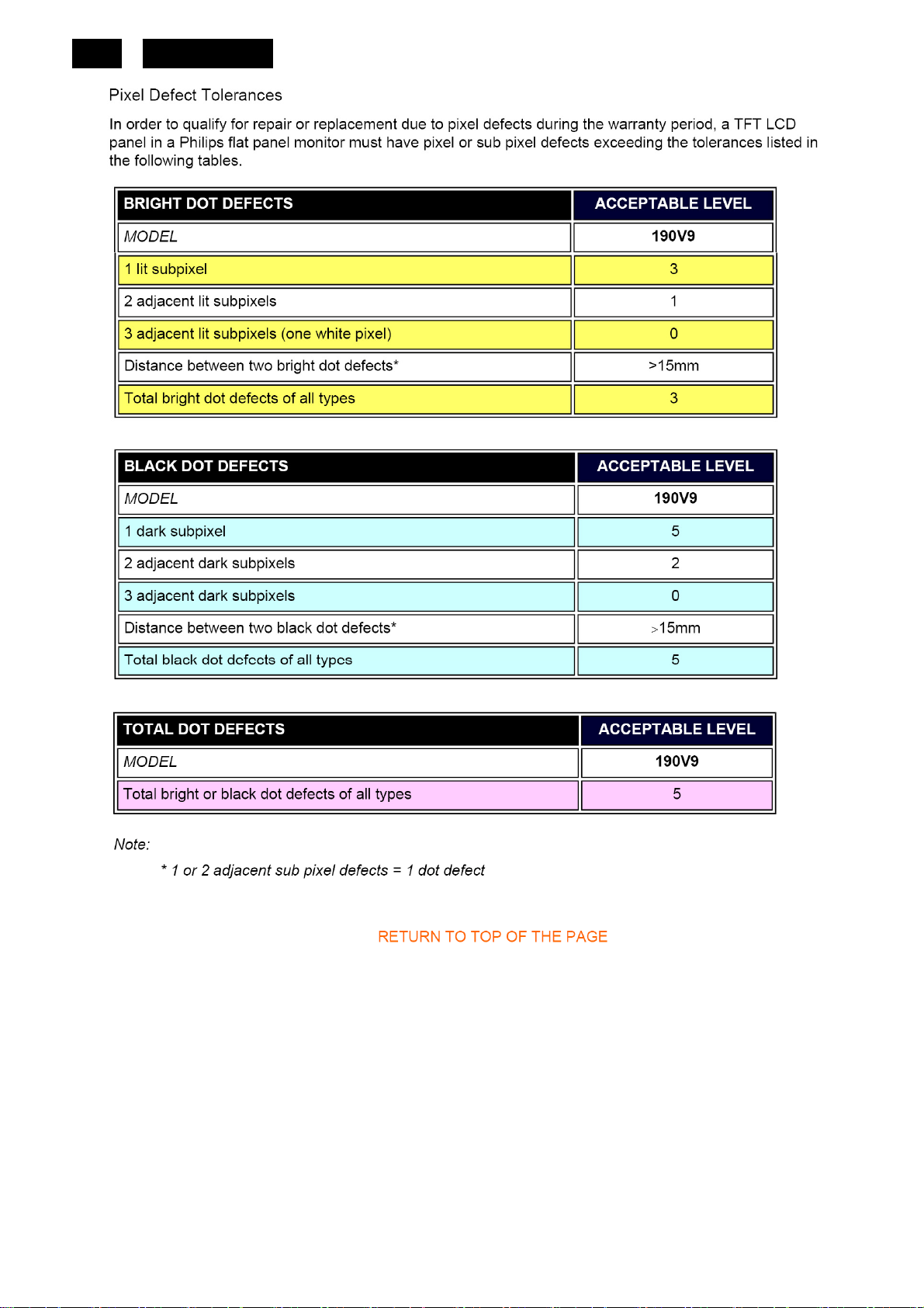
14
HUDSON 9
http://www.wjel.net
Page 15
g
g
g
g
g
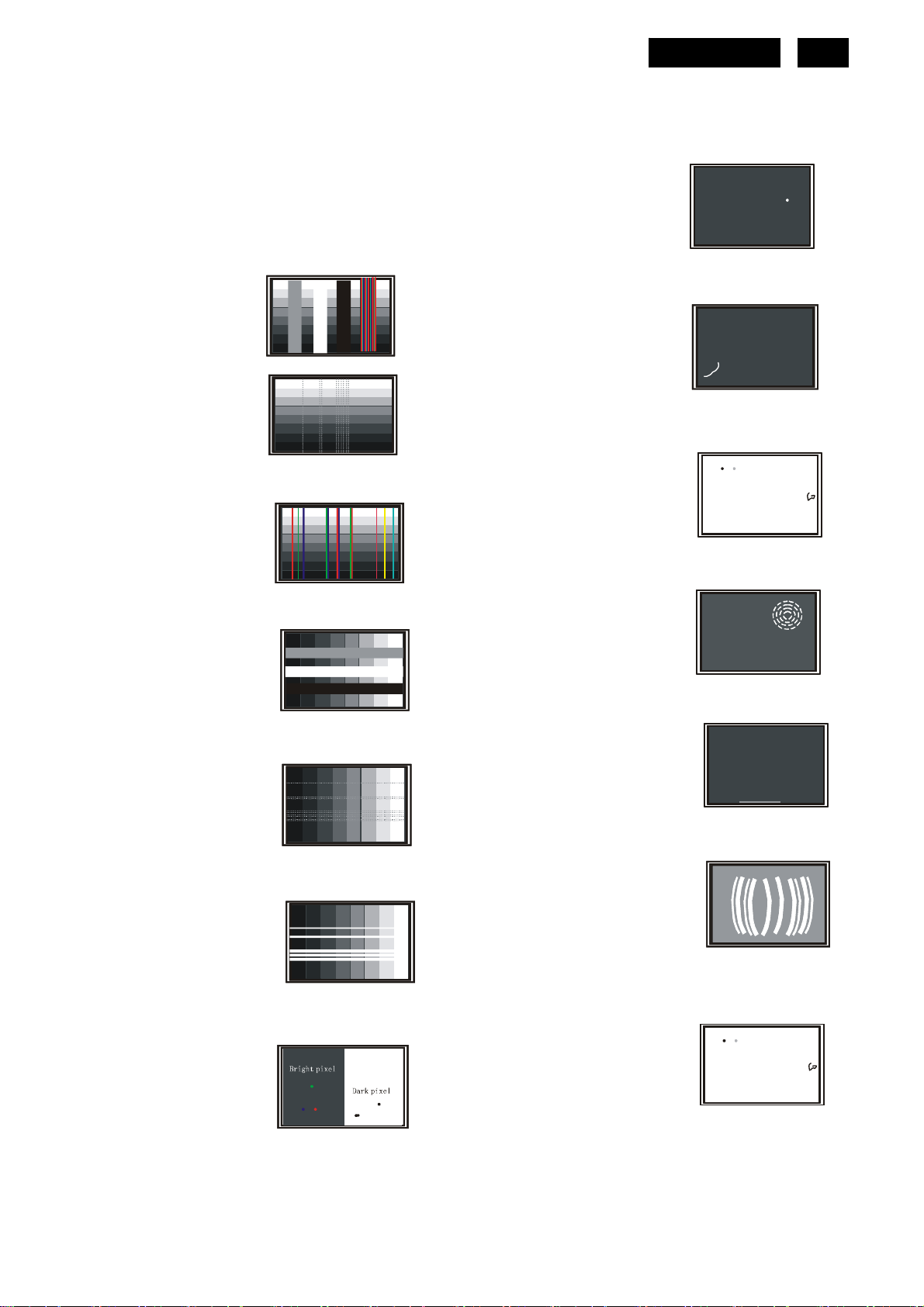
4.4 Failure Mode Of Panel
Quick reference for failure mode of LCD panel
this pa
e presents problems that could be made by LCD panel.
It is not necessary to repair circuit board. Simply follow the mechanical
instruction on this manual to eliminate failure by replace LC D panel.
Polarizer has bubbles
HUDSON 9
15
Failure description
Vertical block defect
Vertical dim lines
Vertical lines defect
(Always bri
Horizontal block defect
ht or dark)
Phenomenon
Polarizer has bubbles
Foreign material inside
polarizer. It shows liner or
dot shape.
Concentric circle formed
Horizontal dim lines
Horizontal lines defect
(Always bri
Has bri
ht or dark)
ht or dark pixel
Bottom back light of LCD is
brighter than normal
Back light un-uniformity
http://www.wjel.net
ht has foreign material.
Backli
Black or white color, liner or
circular type
Page 16
16
HUDSON 9
5. Block Diagram
5.1 Software Flow Chat
1
2
N
4
5
Y
6
7
Y
Y
N
N
3
9
10
Y
N
http://www.wjel.net
18
N
12
Y
14
19
N
13
15
11
17
N
Y
N
Y
16
Y
Page 17
1) MCU initialize.
2) Is the EPROM blank?
3) Program the EPROM by default values.
4) Get the PWM value of brightness from EPROM.
5) Is the power key pressed?
6) Clear all global flags.
7) Are the AUTO and SELECT keys pressed?
8) Enter factory mode.
9) Save the power key status into EPROM.
Turn on the LED and set it to green color.
Scalar initializes.
10) In standby mode?
11) Update the lifetime of back light.
12) Check the analog port, are there any signals coming?
HUDSON 9
17
13) Does the scalar send out an interrupt request?
14) Wake up the scalar.
15) Are there any signals coming from analog port?
16) Display "No connection Check Signal Cable" message. And go into standby mode after the message
disappear.
17) Program the scalar to be able to show the coming mode.
18) Process the OSD display.
19) Read the keyboard. Is the power key pressed?
http://www.wjel.net
Page 18
_
18
HUDSON 9
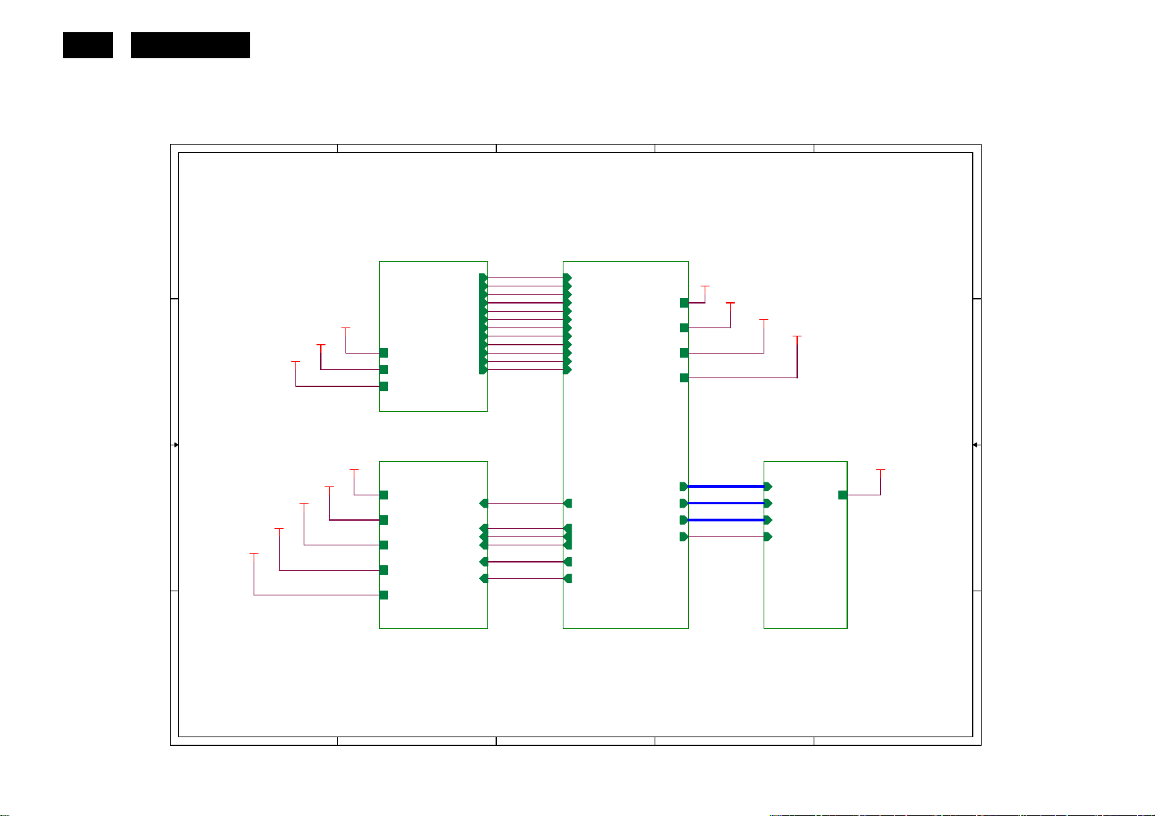
5.2 Electrical Block Diagram
5.2.1 Main Board
Keypad Interface
(CN401)
SST25VF010A-33-4C
Flash Memory
(U402)
(Include MCU, ADC, OSD)
Crystal
14.31818MHZ
(X401)
Panel Interface
(CN403)
Scalar TSUM1PFR-LF
(U401)
D-Sub
Connector
(CN101)
H sync
V sync
RGB
EEPROM
M24C16
(U403)
VGA_SDA,
VGA
SCL
VGA_R+,
VGA_G+,
VGA_B+
EEPROM
AZC099-04S
(U103)
EEPROM
AZC099-04S
(U102)
http://www.wjel.net
Page 19
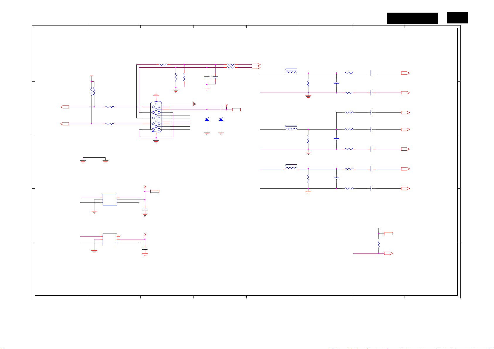
5.2.2 Inverter/Power Board
AC input
EMI filter
Start Circuit: R904、R905、R906
Bridge
Rectifier
and Filter
PWM
Control IC
Transformer
Rectifier
diodes
Feedback
Circuit
HUDSON 9
16V
19
5V
Lamp
Output
Circuit
Transformer
MOSFET
ON/OFF
Feedback
Circuit
Over
Voltage
PWM
Control IC
ON/OFF
Control
DIM
DIM
http://www.wjel.net
Page 20
20
HUDSON 9
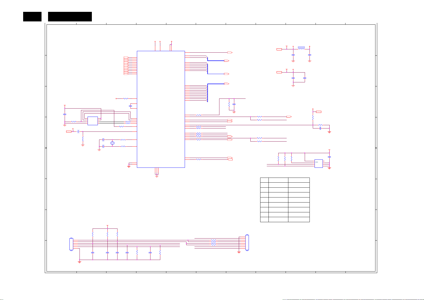
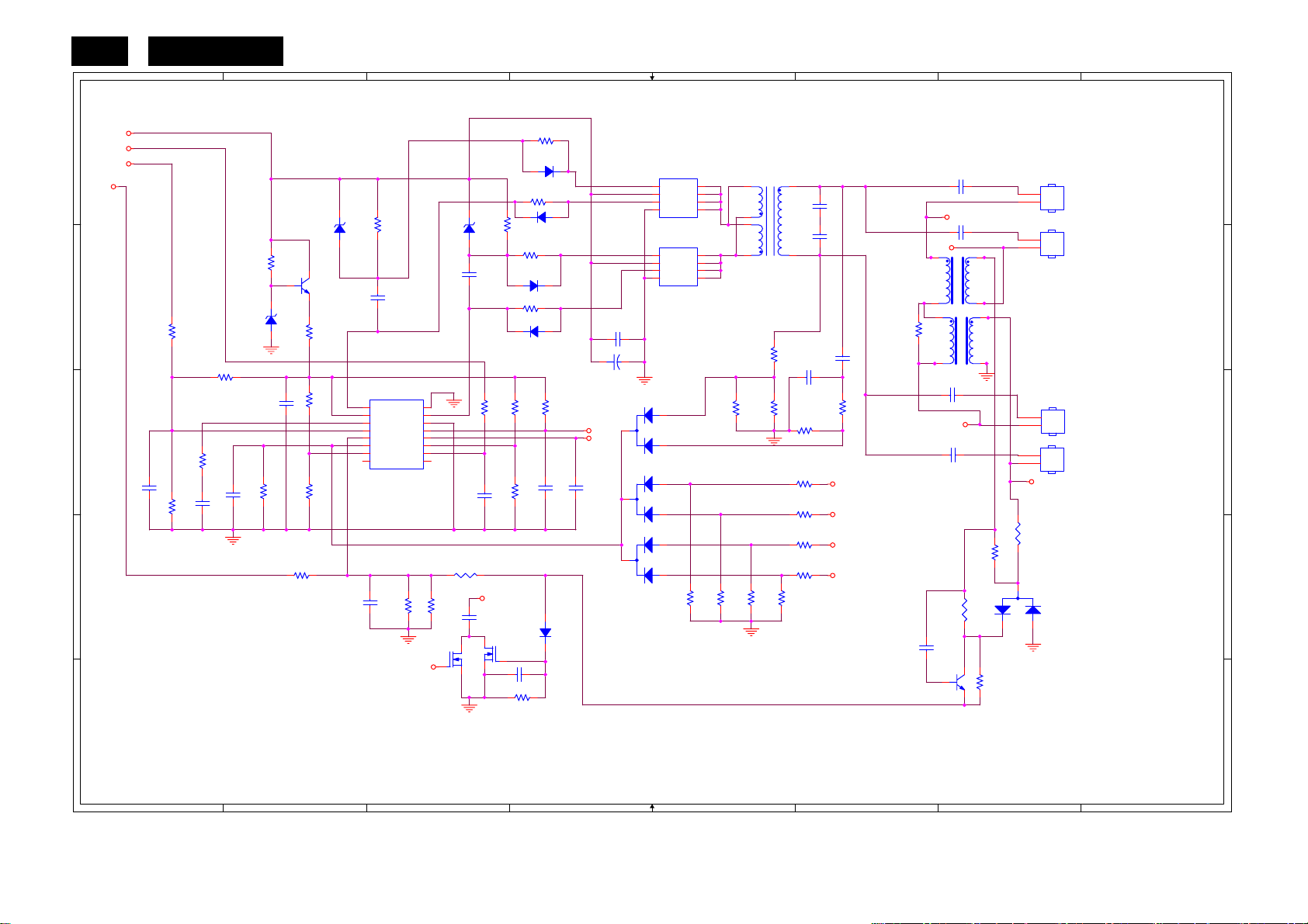
6. Schematic
6.1 Main Board
715G2904-1
1
2
3
4
5
Top
TSUM16FWR SCHEMATIC
A A
XGA/SXGA
LVDS OUTPUT
DSUB_R+
DSUB_R-
DSUB_G+
DSUB_G-
DSUB_SOG
DSUB_5V
CMVCC1
VCC3.3
B B
DSUB_5V
CMVCC1
VCC3.3
DSUB_B+
DSUB_B-
DSUB_H
DSUB_V
DDC1_SDA
DDC1_SCL
DET_CABLE
DSUB_R+
DSUB_R-
DSUB_G+
DSUB_GDSUB_SOG
DSUB_B+
DSUB_BDSUB_H
DSUB_V
DDC1_SDA
DDC1_SCL
DET_CABLE
VCC1.8
VCC3.3
CMVCC
CMVCC1
VCC1.8
VCC3.3
CMVCC
CMVCC1
02.Input
VCC1.8
VCC3.3
DSUB_5V
C C
D D
CMVCC
CMVCC1
VCC1.8
VCC3.3
CMVCC
CMVCC1
05.Power
on_BACKLIGHT
Mute
Volume#
PANEL_ID#DSUB_5V
Adj_BACKLIGHT
VCTRL
on_BACKLIGHT
Mute
Volume#
PANEL_ID#
Adj_BACKLIGHT
VCTRL
03.Scalar
http://www.wjel.net
PA[0..1]
PA[4..9]
PB[0..9]
PPWR_ON#
PA[0..1]
PA[4..9]
PB[0..9]
PA[0..1]
PA[4..9]
PB[0..9]
PPWR_ON#
04.Output
CMVCC
CMVCC
1
2
3
4
5
Page 21
1
2
3
4
5
6
HUDSON 9
7
8
Input
A A
R101 0R05 1/10W 5%
H_Sync
V_Sync
VCC3.3
R121
R120
GND POWER
DSUB_SDA
DSUB_SCL
VGA_G+
10K 1/16W 5%
R110
100R 1/16W 5%
R113
100R 1/16W 5%
DGND
U103
1
I/O1
I/O4
2
GND
VDD
3 4
I/O2 I/O3
AZC099-04S
U102
1
I/O4
I/O1
2
VDD
GND
3 4
I/O2 I/O3
AZC099-04S
DSUB_SCL VGA_PLUG
H_Sync
6
5
V_Sync
6
5
15
14
13
12
11
ESD_VCC
C115
NC
ESD_VCC
VGA_B+VGA_R+
C114
NC
10K 1/16W 5%
DDC1_SCL5
B B
DDC1_SDA5
C C
D D
DDC1_SCL
DDC1_SDA DSUB_SDA
R105
2K2 1/16W 5%
CN101
10
5
9
4
8
3
7
2
6
1
DB15
17 16
ESD_VCC 5
DSUB_5V
VGA_BVGA_B+
VGA_GVGA_G+
VGA_RVGA_R+
R106
2K2 1/16W 5%
ZD103
UDZSNP5.6B
C102
22pF
1 2
R102 100R 1/16W 5%
R103 100R 1/16W 5%
C103
22pF
DSUB_5V
ZD104
UDZSNP5.6B
1 2
DSUB_5V 5
DSUB_H 5
DSUB_V 5
VGA_B+
VGA_B-
VGA_G+
VGA_G-
VGA_R+
VGA_R-
FB102
1 2
BEAD
FB103
1 2
BEAD
FB101
1 2
BEAD
R107
75R 1/16W 5%
R112
75R 1/16W 5%
R116
75R 1/16W 5%
R104
100R 1/16W 5%
C104
5pF/50V
R108
100R 1/16W 5%
R109
390 OHM 1/16W
R111
100R 1/16W 5%
C108
5pF/50V
R114
100R 1/16W 5%
R115
100R 1/16W 5%
C111
5pF/50V
R117
100R 1/16W 5%
VGA_PLUG
C101
0.047uF
C105
0.047uF
C106
0.047uF
C107
0.047uF
C109
0.047uF
C110
0.047uF
C113
0.047uF
VCC3.3
R118
1K 1/16W 5%
VCC3.3 7
DET_CABLE 5
DSUB_B+ 5
DSUB_B- 5
DSUB_SOG 5
DSUB_G+ 5
DSUB_G- 5
DSUB_R+ 5
DSUB_R- 5
CN101 B3
C101 A7
C102 A4
C103 A4
C104 A6
C105 B7
C106 B7
C107 B7
C108 C6
C109 C7
C110 C7
C111 C6
C113 C7
C114 E3
C115 D3
FB101 C5
FB102 A5
FB103 B5
R101 A3
R102 A4
R103 A4
R104 A6
R105 A3
R106 A3
R107 A6
R108 B6
R109 B6
R110 B2
R111 B6
R112 B6
R113 B2
R114 C6
R115 C6
R116 C6
R117 C6
R118 D7
R120 B2
R121 B2
U102 D2
U103 D2
ZD103 B4
ZD104 B4
21
E E
http://www.wjel.net
1
2
3
4
5
6
7
8
Page 22
22
HUDSON 9
1
Scalar
2
3
4
5
6
7
8
9
10
11
A A
AVDD
U401
R403 390 OHM 1/16W
C401
0.1uF/16V
R4560R05 1/16W
R4570R05 1/16W
R401
0R05 1/16W
0R05 1/16W
R402
R428
3.9K OHM 1% 1/16W
C416
C415
0.1uF/16V
0.1uF/16V
13
RIN0P
12
RIN0M
10
GIN0P
9
GIN0M
11
SOGIN0
8
BIN0P
7
BIN0M
16
HSYNC0
17
VSYNC0
18
DDCA_SDA/RS232_TX
19
DDCA_SCL/rs232_RX
4
REXT
15
REFP
14
REFM
21
SDO
22
SCZ
23
SCK
24
SDI
28
GPIO_P27/PWM1
54
RST
1
XIN
2
XOUT
31
MODE[0]
32
MODE[1]
http://www.wjel.net
C417
R404
0.1uF/16V
10K 1/16W 5%
DSUB_R+3
DSUB_R-3
DSUB_G+3
DSUB_G-3
DSUB_SOG3
DSUB_B+3
DSUB_B-3
DSUB_H3
C411 22pF
C412 22pF
VCC3.3
R427
3.9K OHM 1% 1/16W
C414
0.1uF/16V
DSUB_V3
DDC1_SDA3
DDC1_SCL3
AVDD
R405 100R 1/16W 5%
X401
14.31818MHz
1 2
B B
C C
D D
E E
F F
G G
H H
VCC3.3
C408
0.22uF16V
R408
10K 1/16W 5%
CMVCC1
CMVCC17
CN401
CONN
C410
10uF/50V
1
2
3
4
5
6
+
NC/10K 1/16W 5%
U402
1
CE#
2
SO
WP
3
WP#
4 5
VSS SI
SST25VF010A-33-4C-SAE
R417
10K 1/16W 5%
R421
HOLD#
VDD
SCK
8
7
6
C413
NC/0.1uF/16V
VDDP
6
51
VDDP
AVDD_ADC
LVDS
GND
GND
GND
5
29573
TSUM1PFR-LF
R407
10K 1/16W 5%
VDDC
30
GPIO_P10/I2C_MCL
GPIO_P11/I2C_MDA
KEY1
POWER_KEY#
LED_GRN/BLUE
LED_ORANGE
53
VDDC
VDDC
GPIO_P15/PWM0
PWM2/GPIO_P24
GPIO_P12
PWM1/GPIO_P25
GPIO_P00/SAR1
GPIO_P01/SAR2
GPIO_P06
GPIO_P07
PWM0/GPIO_P26
GPIO_P13
GPIO_P14
VCTRL
LVA3P
LVA3M
LVA2P
LVA2M
LVA1P
LVA1M
LVA0P
LVA0M
LVB3P
LVB3M
LVBCKP
LVBCKM
LVB2P
LVB2M
LVB1P
LVB1M
LVB0P
LVB0M
52
PA0
33
PA1
34
PA4
35
PA5
36
PA6
37
PA7
38
PA8
39
PA9
40
PB0
41
PB1
42
PB2
43
PB3
44
PB4
45
PB5
46
PB6
47
PB7
48
PB8
49
PB9
50
R424 100R 1/16W 5%
20
27
55
56
RSTN
R411 100R 1/16W 5%
58
R412 100R 1/16W 5%
59
R414 120R 1/16W 5%
60
R410 120R 1/16W 5%
61
R418 NC/100R 1/16W 5%
62
63
R419 NC/100R 1/16W 5%
64
Max condition for LED:
1. Vcc = 3.3 V
2. Current = 12 mA
FW need to be
modified.
26
R413 100R 1/16W 5%
25
POWER_KEY#
LED_ORANGE
LED_GRN/BLUE
PA[0..1]
PA[4..9]
PB[0..9]
KEY2
KEY1
LED_GRN/BLUE
LED_ORANGE
R429 NC
R430 NC
R431 NC
R432 NC
R425
NC
PA[0..1] 5
PA[4..9] 5
PB[0..9] 5
KEY_LEFT
KEY_RIGHTKEY2
KEY_AUTO
VCTRL 7
EE_WP
C418
NC
on_BACKLIGHT 7
adj_BACKLIGHT 7
Volume# 7
Mute 7
PPWR_ON# 6
DET_CABLE 4
1
2
3
4
5
6
7
8
CN402
NC \ CONN
VCC3.37
VCC1.87
R426 NC/100R 1/16W 5%
R452 100R 1/16W 5%
R420 NC/100R 1/16W 5%
R451 100R 1/16W 5%
MSCL
MSDA
U403
M24C04-WMN6TP
C419
R424 NC100R 1/16W 5%
R433
100R 1/16W 5%
R434
100R 1/16W 5%
R435
10K 1/16W 5%
R436
10K 1/16W 5%
R437
10K 1/16W 5%
VCC3.3
VDDP
FB401
300OHM
C403
0.1uF/16V
VCC1.8
VDDC
C406
0.1uF/16V
R453
10K 1/16W 5%
PANEL_ID# 7
R454
10K 1/16W 5%
R455
10K 1/16W 5%
EE_WP
MSDA
POWER_KEY#
MSCL
For NVRAM Without NVRAM
NC
0.22uF16V
NC
NC
NC
NC
NC
NC
AVDD
C404
0.1uF/16V
C407
0.1uF/16V
CMVCC
CMVCC 7
R406
10K 1/16W 5%
R409
20K OHM 1/16W
C409 0.1uF/16V
VCC3.3
U403
8
VCC
7
WC
6
SCL
M24C16
When NVRAM is used,
POWER_KEY# and PANEL_ID#
will be used for I2C
Bus.
PANEL_ID# and POWER_KEY#
could be optional.
C429
0.22uF16V
1
NC
2
NC
3
NC
45
VSSSDA
CN401 G1
CN402 G7
C401 C3
C403 A9
C404 A9
C406 B9
C407 B9
C408 C1
C409 D10
C410 D1
C411 D2
C412 D2
C413 H2
C414 H2
C415 H3
C416 H3
C417 H4
C418 C7
C429 E10
FB401 A9
R401 D3
R402 D3
R403 C3
R404 H3
R405 D3
R406 C9
R407 H4
R408 D1
R409 D9
R410 D5
R411 D5
R412 D5
R413 E5
R414 D5
R417 D2
R418 D5
R419 D5
R420 D7
R421 G2
R424 C5
R425 C6
R426 C7
R427 G2
R428 G3
R429 G6
R430 G6
R431 G6
R432 H6
R451 D7
R452 D7
R453 E8
R454 E8
R455 E9
R456 D3
R457 D3
U401 A3
U402 C2
U403 E9
X401 D3
Near to Connect
1
2
3
4
5
6
7
8
9
10
11
Page 23
1
2
3
4
HUDSON 9
5
23
Output
A A
PA[0..1]5 PB[0..9]5
PA[4..9]5
B B
C C
PPWR_ON#5
PA[0..1]
PA[4..9]
R435
4K7 1/16W 5%
PPWR_ON#
PA0
PA1
PA4
PA5
PA6
PA7
PA8
PA9
R433
10K 1/16W 5%
Q404
PMBS3906
R436
100K 1/16W 5%
PB[0..9]
C419
0.1uF/16V
CMVCC
Q405
AO3401
CMVCC 7
FB402
120OHM
PB0
PB1
PB2
PB3
PB4
PB5
PB6
PB7
PB8
PB9
PANEL_VCC
C421
+
100uF25V
1
G
AO3401L
PANEL_VCC
R434
330 OHM 1/4W
3
D
2
S
C420
0.1uF/16V
PA0
PA1
PB2
PB3
PA4
PA5
PA6
PA7
PA8
PA9
PB0
PB1
PB2
PB3
PB4
PB5
PB6
PB7
PB8
PB9
CN403
1
2
3
4
5
6
7
8
9
10
11
12
13
14
15
16
17
18
19
20
21
22
23
24
25
26
27
28
29
30
CONN
CN403 A5
C419 C2
C420 A4
C421 C3
FB402 C3
Q404 C2
Q405 C3
R433 C2
R434 A4
R435 C1
R436 C2
D D
http://www.wjel.net
1
2
3
4
5
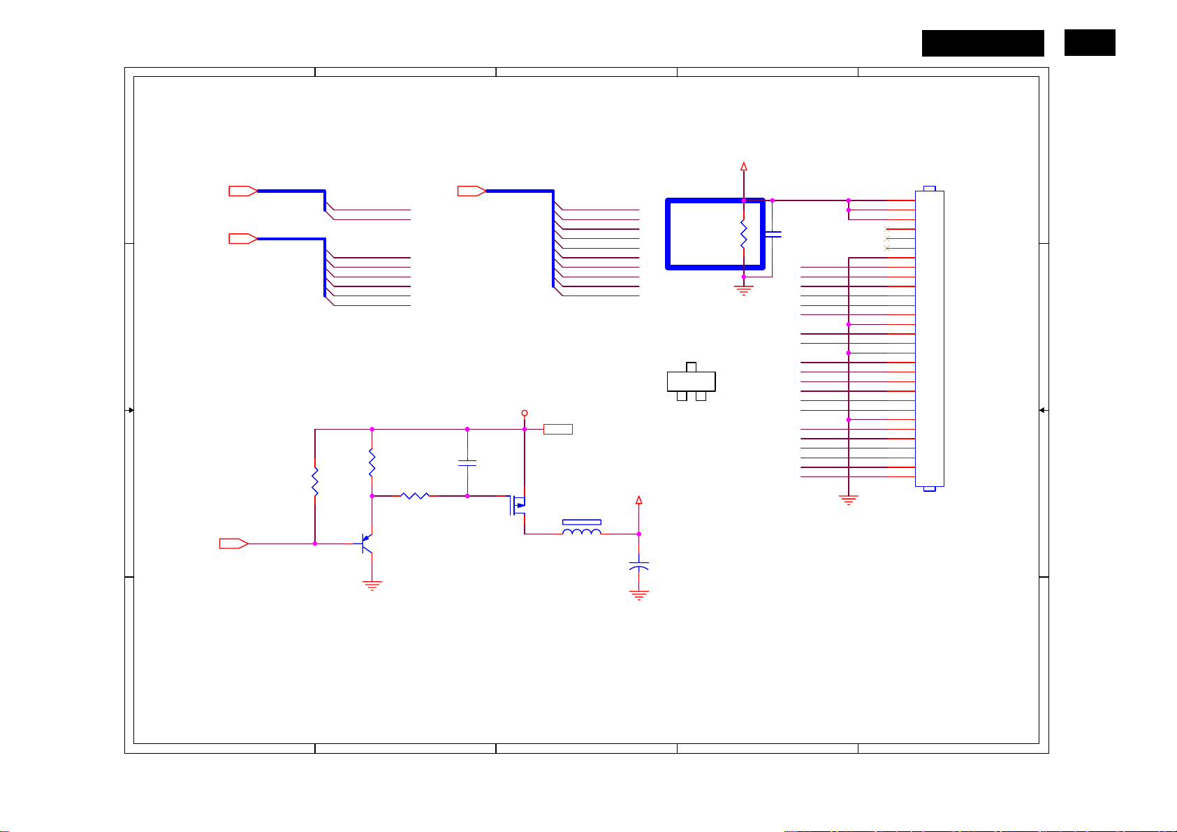
Page 24
24
HUDSON 9
1
2
3
4
5
6
7
8
Power
Due to LG doen't request PC'99 Function.
A A
ESD_VCC 2
CMVCC
CMVCC5, 6
CN404
1
2
CMVCC
3
CONN
4
5
6
7
8
9
BKLT-VBRI
BKLT-EN
C_PANEL_INDEX
Volume
Mute
R450 NC
B B
SM340A
D402
R458
NC
NC(R0402)
DSUB_5V
2
3
PANEL_ID# 5
1
CMVCC1
D401
BAV99
R449
NC
DSUB_5V 2
CMVCC1 5
Mute 5
VCC3.3 VCC3.3
R437
C425
NC
10K 1/16W 5%
Q406
2N3904S-RTK/PS
BKLT-ENCMVCC
R440
4K7 1/16W 5%
R439
10K 1/16W 5%
on_BACKLIGHT 5
LG
OTHER NC
VCTRL5
NC
BAV99
VCC3.3
D401
0Ohm 1/16W
Q410
KN2907AS
Q409
KN2907AS
R458
C432
0.1uF/16V
VCC1.8
C423
+
100uF25V
VCC1.8 5
CN404 B1
C422 D6
C423 B7
C425 B3
C426 D5
C427 D7
C428 D5
C432 B7
D401 A2
D402 B2
FB403 C6
Q406 B4
Q408 D3
Q409 B6
Q410 B6
R437 B4
R439 B4
R440 B4
R441 C1
R442 D1
R446 C3
R447 C4
R448 D4
R449 B3
R450 B2
R458 A2
U404 C6
C C
VCC3.3
R446
R441
1K 1/16W 5%
BKLT-VBRI
D D
R442
100R 1/16W 5%
adj_BACKLIGHT 5
Volume
NC
Q408
NC/2N3904S-RTK/PS
VCC3.3VCC3.3
R448
NC/4K7 1/16W 5%
R447
NC/10K 1/16W 5%
Volume# 5
CMVCC1
+
C426
100uF25V
MVCC
C428
0.1uF/16V
FB403 NC
VIN
VOUT
ADJ(GND)
U404
AP1117D33LA
VCC3.3
3
2
1
C422
0.1uF/16V
+
VCC3.3 4, 5
C427
100uF25V
U404 can use package 232 or 252.
E E
http://www.wjel.net
1
2
3
4
5
6
7
8
Page 25
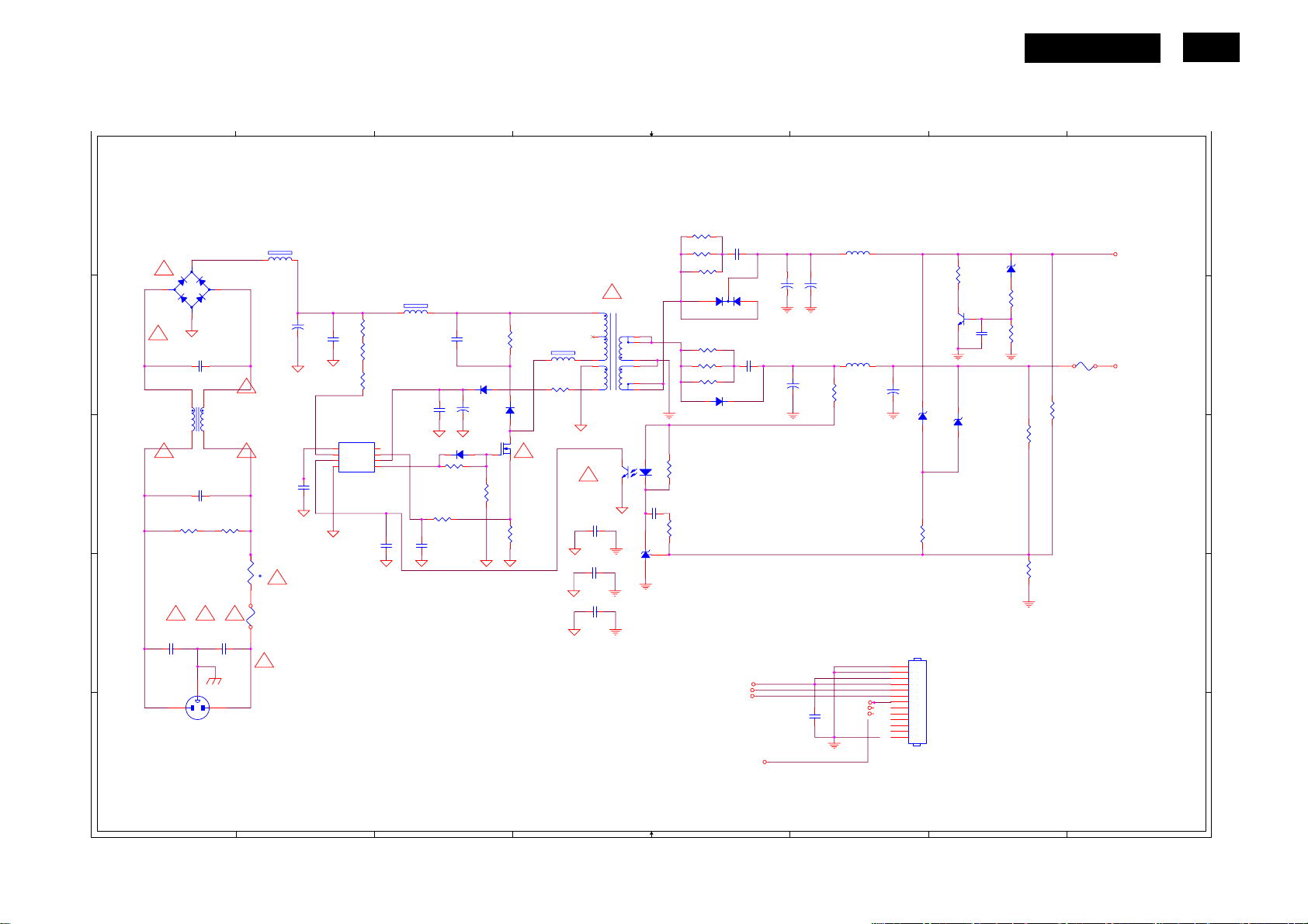
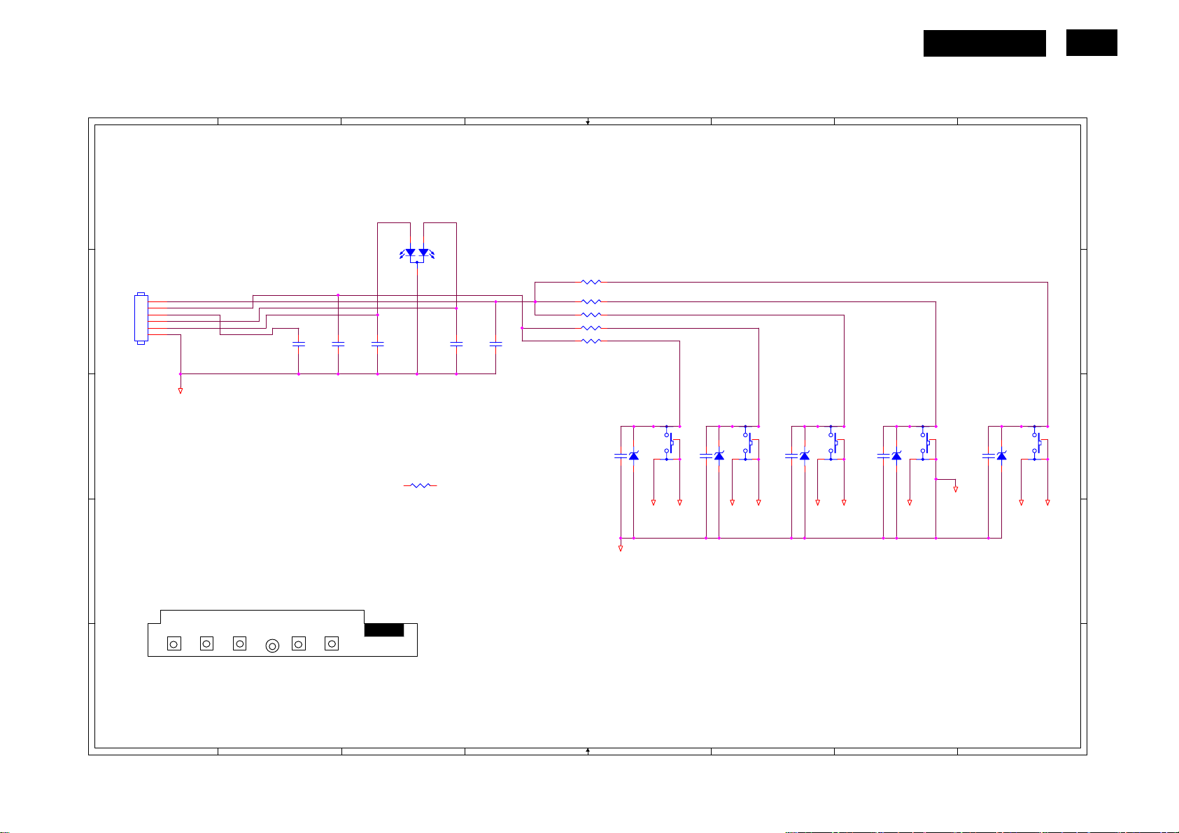
HUDSON 9
6.2 Power Board
715G2824-1
1
Power
A A
2
3
4
5
6
7
8
25
FB904
3
R901
BD901
KBP208G
!
1000pF
!
!
1 2
12
NR901
NTCR
t
F901
FUSE
BEAD
R915
0.047uF/25V
!
+
C905
100uF450V
c938
NC
1500P/2KV
IC901
4 5
RT NC
3
VCC
2
COMP
1
GND
LD7552DPS
R904
300K OHM 1/4W
R905
300K OHM 1/4W
R906
300K OHM 1/4W
6
CS
7
VCC
8
OUT
C928
1000pF
FB902 80OHM
1 2
C907
0.1uF
D903
R910
10R 1/4W
R912
220 OHM 1/4W
C909
470pF/25V
C906
1500pF2KV
D901
FR103
+
C908
22uF/50V
1N4148W
100K OHM 2W
R938
10K 1/8W
R903
D900
PR1007R
Q901
!
STP9NK65ZFP
R914
0.43 5% 2W
FB903
1 2
BEAD
R909
5.1 OHM 1/4W
4
5
6
1
3
!
C921
NC
C900
2200pF 250V
C920
1000pF 250V
!
T901
POWER X'FMR
PC123X2YFZOF
1
!
+
2
-
4
B B
!
C904
NC
1
4
L901
30.0mH
2
3
!
1M 1/4W
!
C901
1000pF
R902
C903
0.47uF/275V
1M 1/4W
!
C902
C C
D D
!
3
12
CN901
SOCKET
E E
http://www.wjel.net
R918100 OHM 1/4W
R919100 OHM 1/4W
R920100 OHM 1/4W
8
7
9
10
12
11
IC903
12
43
C924
0.1uF
IC904
AZ431AZ-AE1
R925
1K 1/8W
R926
1K 1/10W 1%
C912
0.001uF
2
3
D906A
FCH10U15
R935 100 OHM 1/4W
R961 100 OHM 1/4W
R962 100 OHM 1/4W
D907
31DQ06FC3
+5V
DIM
ON/OFF
1
1000uF/25V
+5V1
C917
680uF25V
C929
0.001uF
C939
+
+
C931
0.1uF
+
C918
680uF25V
L904
3.5uH
L903
3.5uH
R924
150R 1/8W 5%
MUTE
470uF/16V
PID
VOL
C915
F903
FUSE
+16V
+5V
BD901 A1 CN901 D1
CN902 D6 C900 D4
C901 D1 C902 D1
C903 C1 C904 B1
C905 B2 C906 B3
C907 B3 C908 B3
C909 C3 C912 A5
C915 B6 C917 B5
C918 B6 C920 D4
C921 C4 C924 C4
C928 C3 C929 B5
C931 E6 C932 B7
C939 B5 D900 B3
D901 B3 D903 C3
D906A B5 D907 B5
FB902 B3 FB903 B4
FB904 A2 F901 D2
F903 B7 IC901 C2
IC903 C4 IC904 C4
L901 B1 L903 B6
L904 A6 NR901 D2
Q901 C3 Q903 B7
R901 C1 R902 C1
R903 B3 R904 B2
R905 B2 R906 B2
R909 B4 R910 C3
R912 C3 R914 C3
R915 C2 R918 A5
R919 A5 R920 A5
R924 B6 R925 C5
R926 C5 R927 C7
R930 D7 R935 B5
R938 C3 R939 B7
R940 B7 R942 C6
R943 B7 R946 A7
R961 B5 R962 B5
T901 B4 ZD902 A7
ZD921 B6 ZD922 B7
R946
150OHM2W
Q903
PMBS3904
+
ZD922
RLZ5.6B
ZD921
RLZ22B
1 2
1 2
R942
1K 1/10W 1%
CN902
1
2
3
4
5
6
7
8
9
10
11
12
13
CONN
C932
0.001uF
ZD902
RLZ18B
R943
470R 1/8W
R939
1K 1/8W
R940
NC
R927
2.43K OHM 1% 1/10W
R930
2.43K OHM 1% 1/10W
1
2
3
4
5
6
7
8
Page 26
26
Inverter
HUDSON 9
1
2
3
4
5
6
7
8
+16V
ON/OFF
A A
DIM
PID
R801
2.4K OHM 1/10W
B B
C C
D D
E E
R813
470K 1/10W 5%
C803
NC
R815
NC
R816
10K 1/10W 1%
C804
2.2uF/16V
R814
NC
C805
0.01uF
ZD801
RLZ5.6B
1 2
C806
1uF/16V
R817
1M 1/10W 5%
R850
100K 1/10W 5% /NC
Q801
PMBS3904
R802
22R 1/8W
100K 1/10W 5%
ZD802
RLZ5.6B
5K1 1/8W
1 2
R818
R819
100K 1/10W 5%
C813
33NF 25V
R803
C801
0.047uF
IC801
1
DRV1
PGND
2
VDDA
DRV2
3
TIMER
GNDA
4
DIM
5
ISEN
SSTCMP
6
VSEN
LCT
7
OVPT
ENA
8 9
NC1 NC2
OZ9938GN
R823
510R 1/10W 1%
CT
SST
16
15
14
13
12
11
10
Q802
RK7002
1 2
R825
510R 1/10W 5%
R824
6.8K 1/10W
ZD803
RLZ5.6B
C802
0.047uF
D804 1N4148W
R820
20K 1/10W 5%
C807
1uF
CT
C814
390P 50V
RK7002
Q803
C815 0.047uF
R805
100R 1/10W 5%
D801 1N4148W
R806 100R 1/8W
R804 5K1 1/8W
R807 100R 1/10W 5%
D803 1N4148W
R808 100R 1/8W
R822
20K OHM 1% 1/8W
R821
1M 1/10W 5%
C808
180K 1/10W
C809
560pF50V
D805
R826
1M 1/10W 5%
D802 1N4148W
C810
0.047uF
1N4148W
CT
SST
C811
0.1uF
C812
+
1000uF 25V
3
D807
3
D808
3
Q805
4
G
3
S
2
G
1
S
AM4502C-T1-PF
Q806
4
G
3
S
2
G
1
S
AM4502C-T1-PF
D806
2
1
2
BAV70
1
2
BAV70
1
10K 1/10W 5%
BAV70
10K 1/10W 5%
R842
5
D
6
D
7
D
8
D
5
D
6
D
7
D
8
D
R843
6.2M OHM 1/2W
R829
6K8 1/8W
10K 1/10W 5%
R844
6
2
5
PT801
POWER X'FMR
R828
R830
NC
8
C816
22pF/6KV
C824
22pF/6KV
91
C817
2pF/3KV
C818
220pF
R836
62K 1/10W 5%
R837
8K2 1/10W
R838 1M 1/10W 5%
R839 1M 1/10W 5%
R840 1M 1/10W 5%
R841 1M 1/10W 5%
10K 1/10W 5%
LV2
R845
C819
68pF/3KV
LV1
C820
68pF/3KV
L801
LV2
1
Line Filter
2 3
1
NC
R827
2 3
Line Filter
LV1
LV3
LV4
RST CHIP MAX 0R05 1/10W
C823
NC
Q804
NC
R846
L802
C821
22pF/3KV
LV3
C822
22pF/3KV
R848
NC
4
4
RST CHIP MAX 0R05 1/10W
CN801
1
2
CN802
1
2
CN803
1
2
1
2
CN804
LV4
R847
NC
3
D809
BAV99
1
2
R849
CN801 A7 CN802 A7
CN803 C7 CN804 C7
C801 B3 C802 B3
C803 C1 C804 C1
C805 C2 C806 C2
C807 C3 C808 C3
C809 C4 C810 C4
C811 B4 C812 B4
C813 D2 C814 D3
C815 D4 C816 A6
C817 B6 C818 B6
C819 A7 C820 A7
C821 C6 C822 C7
C823 D6 C824 B6
D801 A4 D802 A4
D803 B4 D804 B4
D805 D4 D806 C4
D807 C4 D808 D4
D809 D7 IC801 C3
L801 B6 L802 B6
PT801 A5 Q801 B2
Q802 D3 Q803 D3
Q804 E7 Q805 A5
Q806 B5 R801 B2
R802 B2 R803 A3
R804 A3 R805 A4
R806 A4 R807 B4
R808 B4 R813 B1
R814 B1 R815 C1
R816 C1 R817 C2
R818 C2 R819 C2
R820 C3 R821 C3
R822 C4 R823 D3
R824 D3 R825 D3
R826 E4 R827 B6
R828 B5 R829 C5
R830 C5 R836 C6
R837 C5 R838 C5
R839 C5 R840 D5
R841 D5 R842 D5
R843 D5 R844 D5
R845 D5 R846 D7
R847 C7 R848 D7
R849 E7 R850 D2
ZD801 B2 ZD802 A2
http://www.wjel.net
1
2
3
4
5
6
7
8
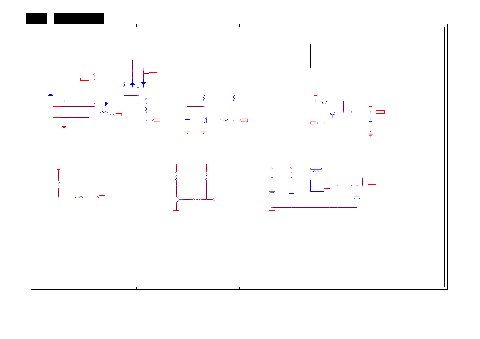
Page 27
HUDSON 9
6.3 Key Board
715G3016-1
1
A A
2
3
4
5
6
7
27
8
LED_RED#
CN001
LBADC1
1
LBADC2
2
DC_POWERON
CONN
3
4
5
6
LED_GRN#
LED_RED#
SGND
C001
NC/0.001uF
C002
NC/0.001uF
C003
NC/0.001uF
B B
C C
D D
CONNECTOR
(MENU) LED(Power)
E E
(OK)(UP) (DOWN)
LED_GRN#
1
3
LED001
LED
2
R007 0R05 1/4W
C004
NC/0.001uF
C005
NC/0.001uF
R001 4.3K OHM 1% 1/8W
R002 2.4K OHM 1% 1/8W
R003 910R 1/8W
R004 4.3K OHM 1% 1/8W
R005 2.4K OHM 1% 1/8W
ZD002NC/UDZS5.6B
C007NC/0.1uF
SGND SGND
GND
SW005
3 4
SW002
ZD004NC/UDZS5.6B
3 4
DOWN
21
5
SW
OK
21
5
SW
C008NC/0.1uF
SW004
UP
21
5
SW
ZD005NC/UDZS5.6B
C009NC/0.1uF
3 4
SW001
MENU
21
5
SW
ZD001NC/UDZS5.6B
C006NC/0.1uF
3 4
SGND SGND SGNDSGND SGND SGNDSGND
SGND
CN001 B1 C001 B2
C002 B2 C003 B3
C004 B3 C005 B4
C006 C7 C007 C5
C008 C5 C009 C6
C010 C8 LED001 A3
R001 B4 R002 B4
R004 B4 R005 B4
R007 C3 SW001 C7
SW002 C6 SW003 C8
SW004 C6 SW005 C5
ZD001 C7 ZD002 C5
ZD003 C8 ZD004 C5
SW003
SW
ZD003NC/UDZS5.6B
C010NC/0.1uF
3 4
http://www.wjel.net
POWER
21
5
1
2
3
4
5
6
7
8
Page 28
28
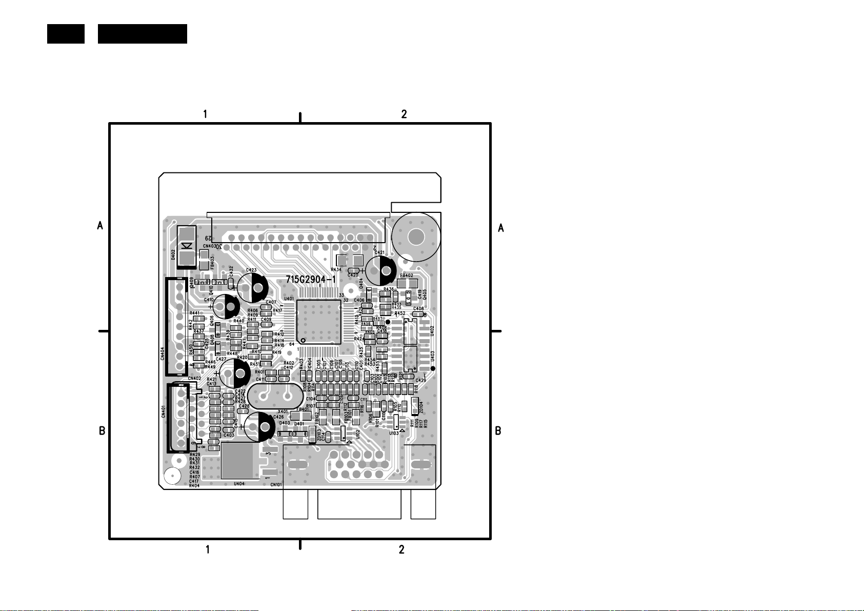
HUDSON 9
7. PCB Layout
7.1 Main Board
715G2904-1
C101 B2 FB101 B2 R418 B1
C102 B2 FB102 B2 R419 B1
C103 B2 FB103 B2 R420 B1
C104 B2 FB401 B2 R421 B1
C105 B2 FB402 A2 R424 B2
C106 B2 FB403 A1 R425 B2
C107 B2 FDT2 ?1 R426 A2
C108 B2 FDT3 ?6 R427 B1
C109 B2 Q404 A2 R428 B1
C110 B2 Q405 A2 R429 B1
C111 B2 Q406 B1 R430 B1
C113 B2 Q408 B1 R431 B1
C114 B2 Q409 A1 R432 B1
C115 B2 Q410 A1 R433 A2
C401 B2 R101 B2 R434 A2
C403 B1 R102 B2 R435 A2
C404 B2 R103 B2 R436 A2
C406 A2 R104 B2 R437 B1
C407 A1 R105 B2 R439 B1
C408 A2 R106 B2 R440 A1
C409 A1 R107 B2 R441 A1
C410 A1 R108 B2 R442 A1
C411 B1 R109 B2 R446 B1
C412 B1 R110 B2 R447 B1
C413 B1 R111 B2 R448 B1
C414 B1 R112 B2 R449 B1
C415 B1 R113 B2 R450 B1
C416 B1 R114 B2 R451 B1
C417 B1 R115 B2 R452 A2
C418 B2 R116 B2 R453 B2
http://www.wjel.net
C419 A2 R117 B2 R454 B2
C420 A2 R118 B2 R455 B2
C427 B1 R404 B1 SEN3 A2
C428 B1
R405 B2
SEN4 B1
C429 B2
R406 A1
U102 B2
C432 A1
R407 B1
U103 B2
CN101 B2
R408 B2
U401 A2
CN401 B1
R409 B1
U402 A2
CN402 B1
R410 B1
U403 B2
CN403 A1
R411 B1
U404 B1
CN404 A1
R412 B1
X401 B1
D401 B2
R413 A2
ZD103 B2
D402 A1
R414 B1
ZD104 B2
D403 B1
R417 A1
Page 29
HUDSON 9
29
http://www.wjel.net
Page 30

30
HUDSON 9
7.2 Power Board
715G2824-1
BD901 D3 J821 B2
BD901A D3 J823 B1
BD901B D3 J824 B2
C604 D4 J825 C2
C812 B2 J826 D1
C816 C1 J829 C4
C817 B1 J830 D1
C819 A1 J831 D1
C820 B1 J832 D4
C821 C1 J833 D3
C822 C1 J834 D1
C824 C1 J835 D4
C900 B3 J836 C4
C901 D2 J837 D4
C902 D2 J838 D4
C903 D2 J901 C4
C905 C3 J902 C3
C905A C3 J903 C3
C906 B3 J904 B2
C908 C2 J905 B3
C915 A4 J906 B2
C916 A4 J907 A2
C917 A2 J908 A2
C918 A2 J909 A4
C920 B2 J910 A4
C921 B4 J911 B4
C934 B4 J912 B4
C938 C3 L801 A1
C939 B3 L802 D1
CN601 D3 L901 D2
http://www.wjel.net
CN602 D4 L903 A3
CN801 A1 L904 A3
CN802 B1 L905 B4
Page 31

HUDSON 9
31
C601 D3 R818 A2
C602 D4 R819 A2
C603 D4 R820 A2
C606 D3 R821 A2
C608 D3 R822 B2
C609 D3 R823 A2
C610 D3 R824 A2
C611 D3 R825 B2
C612 D3 R826 B2
C613 D3 R827 D1
C801 B2 R829 C1
C802 C2 R830 C1
C803 B2 R836 B1
C804 B2 R837 A1
C805 A2 R838 A1
C806 B2 R839 A1
C807 A2 R840 A1
C808 A2 R841 A1
C809 B2 R842 A1
C810 A2 R843 A1
C811 B2 R844 A1
C813 A2 R845 A1
C814 B2 R846 D1
C815 B2 R847 D1
C818 B1 R848 D1
C823 D1 R849 D1
C907 C3 R850 A2
C909 C3 R901 C2
C912 A2 R902 D2
C924 B2 R904 C3
C928 C3 R905 C3
C929 A3 R906 C3
C930 B4 R909 B3
C931 A4 R910 C3
C932 A3 R912 C3
http://www.wjel.net
C935 B4 R915 C3
C940 C4 R918 B2
D801 C2 R919 B2
D802 B2 R920 B2
D803 C2 R924 B2
D804 C2 R925 B2
D805 B2 R926 B2
D806 A2 R927 B2
D807 A1 R930 B2
D808 A2 R935 B3
D809 D1 R938 B4
D903 C3 R939 A3
FB902 C3 R940 B2
IC801 B2 R942 B2
IC901 C3 R943 A3
J802 A2 R949 B4
Q601 D3 R950 B4
Q801 A2 R951 B4
Q802 B2 R961 B3
Q803 B2 R962 A3
Q804 D1 RJ610 D3
Q805 B2 RJ801 A2
Q806 C2 RJ802 A2
Q903 A3 RJ804 D1
R601 C4 RJ805 A2
R602 D4 RJ901 C3
R603 D4 SG12 =4
R604 D3 SG13 D2
R605 D3 SG14 D2
R606 D3 SG15 D2
R607 D3 SG16 D2
R608 D3 SG18 D1
R609 D3 SG19 D2
R610 C4 SG20 D2
R801 A2 SG21 D2
R802 A2 SG22 D2
R803 C2 SG23 D2
R804 C2 SG24 D2
R805 C2 SG25 D2
R806 B2 SG26 C2
R807 C2 SG27 C2
R808 C2 ZD801 A2
R813 A2 ZD802 C2
R814 A2 ZD803 C2
R815 B2 ZD902 A3
R816 B2 ZD921 B2
R817 A2 ZD922 B2
Page 32

32
HUDSON 9
7.3 Key Board
715G3016-1
CN001 A3
GND1 A1
GND2 A3
LED001 A2
SW001 A1
SW002 A2
SW003 A1
SW004 A2
SW005 A3
C001 A3
C002 A2
C003 A2
C004 A3
C005 A1
C006 A1
C007 A3
C008 A2
C009 A2
C010 A1
R001 A1
R002 A1
R003 A2
R004 A2
R005 A2
R007 A3
http://www.wjel.net
ZD001 A1
ZD002 A3
ZD003 A1
ZD004 A2
ZD005 A2
Page 33

6
A
8. Wiring Diagram
HUDSON 9
33
CN802
CN801
CN804
CN803
Power Board
CN901
CN902
C IN
1
14Pin
14
HARNESS 14P (SAN)-9P
95G 82014X507
HARNESS6P (SANW)-6P
95G820H 6D509
89G179J30N501
FFC Cable
30
30 Pin
CN403
1
1
9Pin
9
1
Pin
6
CN404
6
CN401
Main Board
TSUM1PFR-LF
U401
CN101
D-SUB
6
Pin
Key Board
1
CN001
http://www.wjel.net
Page 34

34
HUDSON 9
9. Scalar Board Overview
DC-DC Converters
DC-DC Converters
D-SUB
Morning Star chip
D-SUB
http://www.wjel.net
EEPROM
Flash ROM
Page 35

HUDSON 9
10. Mechanical Instructions
1. Back View as Fig1
Place the monitor face down on a smooth surface as Fig 1. Be careful to avoid scratch and injury during the
35
uninstallation.
Fig1
2. Remove the hinge as Fig2.
Remove the three screws remarked in red to remove the hinge as Fig2.
http://www.wjel.net
Fig2
Page 36

36
3. Remove bezel and rear cover as Fig3~ Fig5.
HUDSON 9
Fig3
http://www.wjel.net
Fig4
Page 37

Fig5
HUDSON 9
37
4. Remove main frame cover as Fig6~Fig7.
a. Remove the two screws marked in red as Fig6.
b. Disconnect the four connector marked in blue as Fig6.
c. Remove the two screws marked in red as Fig7.
Fig6
http://www.wjel.net
Fig7
Page 38

38
5. Remove power board as Fig8.
a. Remove the two screws marked in red as Fig8.
b. Disconnect the connector marked in blue as Fig8.
6. Remove scalar board as Fig9~Fig10.
HUDSON 9
Fig8
a. Remove the screw remarked in red as Fig9.
b. Disconnect the two connectors marked in blue as Fig9.
c. Remove the two screws remarked in red as Fig10.
Fig9
http://www.wjel.net
Fig10
Page 39

11. Trouble Shooting
This page deals with problems that can be corrected by a user. If the problem still persists after you
have tried these solutions, contact Philips customer service representative.
HUDSON 9
39
http://www.wjel.net
Page 40

40
HUDSON 9
http://www.wjel.net
Page 41

12. Repair Flow Chart
12.1 Main Board
(1). No Power
No power
HUDSON 9
41
Press power key and look
if the picture is normal
NG
Please reinsert and make sure
the AC of 100-240 is normal
OK
NG
Reinsert or check the
Adapter/Inverter section
Measure U404 PIN2=3.3V
Q409 V
OK
collector
=1.8V
NG
Check U404, Q409 and Q410
X401 oscillate waveforms
are normal
NG
OK
Replace X401
http://www.wjel.net
Replace U401
Page 42

42
(2). No Picture
No picture
HUDSON 9
The button if
under control
OK
Measure U404 PIN2=3.3V
Q409 V
OK
X401 oscillate
waveform is normal
collector
NG
NG
=1.8V
Check U404, Q409 and Q410
X401 oscillate
waveform is normal
Check reset circuit of
U401 is normal
Replace U401
OK
OK
NG
NG
Replace X401
Check Correspondent
component
OK
NG
Replace X401
Check HS VS from
Replace U401
CN101 is normal
OK
Replace U401
NG
Check Correspondent
component
http://www.wjel.net
Page 43

p
p
(3). White screen
HUDSON 9
43
Check Correspondent
com
onent.
White screen
Measure Q404 base
is low level?
OK
Check Q404, Q405 is broken
or CN403 solder?
NG
OK
Replace Panel
NG
X401 oscillate
waveform is normal
NG
OK
Check reset circuit of
U401 is normal
NG
OK
Replace U401
Replace X401
Check Correspondent
com
onent.
http://www.wjel.net
Page 44

44
HUDSON 9
11.2. Power/Inverter Board
(1) No power
Check ZD902 (-) = 16V
NG
Check AC line volt 110V or 220V
OK
NG
Check AC input
Check the voltage of C905 (+)
OK
NG
Check bridge rectified circuit and F901 circuit
Check start voltage for the pin3 of IC901
OK
NG
Check R904, R905, R906 and Change IC901
Check the auxiliary voltage is bigger than
10V and smaller than 20V
OK
NG
1) Check IC901
2) Check R909, D901 circuit
Check IC901 pin8 PWM wave
http://www.wjel.net
OK
NG
Check IC901
Check Q901, D903, IC903, IC904, ZD921, ZD922
Page 45

(2) W / LED, No Backlight
HUDSON 9
45
Check CN902 pin4 = 16V
OK
NG
Check adapter or MB
Check ON/OFF signal
OK
NG
Check Interface board
Check IC801 PIN2=5V
OK
NG
Check Q801 and ZD801
Check IC801 PIN1, 15 have the output of square wave at short
OK
NG
Change IC801
Check Q805 and Q806 PIN5, 6, 7, 8 have the output of square wave at short time.
NG
OK
Check Q805, Q806
Check the output of PT801
http://www.wjel.net
OK
NG
Change PT801
Check connecter & lamp
Page 46

46
12.3 Key Board
HUDSON 9
Is Key Pad Board connecting normally?
OSD is unstable or not working
Y
Is Button Switch normally?
Y
Is Key Pad Board normally?
Y
N
Connect Key Pad Board
N
Replace Button Switch
N
Replace Key Pad Board
Check Main Board
http://www.wjel.net
Page 47

13. ISP Instruction
1. When do the part, need the tools as follow:
HUDSON 9
47
a. An i486 (or above) personal computer or compatible.
b. Microsoft operation system Windows 95/98/2000/XP.
c. “ PORT95NT.exe” program
d. Software ISP SN Alignment kits
The kit contents:
a. ISP BOARD x1
b. Printer cablex1
c. VGA cable x1
2. Install the “PORT95NT.EXE”, and restart the computer.
You must install the
at the first. The processing as follows:
http://www.wjel.net
Page 48

48
HUDSON 9
http://www.wjel.net
Page 49

HUDSON 9
49
http://www.wjel.net
Page 50

50
HUDSON 9
http://www.wjel.net
Click to complete the installation.
Page 51

HUDSON 9
51
Note: After installation, you must restart the PC to take the setup to effect.
3. Connect the ISP board as follow:
Connect to
the PC LPT
http://www.wjel.net
Connect to the
Philips 190V9
Page 52

52
4. The process of ISP write is as follows.
a. Double-click ,running the program as follows:
HUDSON 9
http://www.wjel.net
Page 53

b. Click icon, search the program” 190V9_TSUM1PFR_LM190E08_TLL_20080319_V101”, and click
open:
HUDSON 9
53
http://www.wjel.net
Page 54

54
c. Click icon, it will auto run. If burn in success, it will show as the follow picture:
HUDSON 9
http://www.wjel.net
Page 55

HUDSON 9
14. DDC Instruction
General
DDC Data Re-programming
In case the main EEPROM with Software DDC which store all factory settings were replaced because a defect,
repaired monitor’ the serial numbers have to be re-programmed.
It is advised to re- soldered the main EEPROM with Software DDC from the old board onto the new board if
circuit board have been replaced, in this case the DDC data does not need to be re-programmed.
Additional information about DDC (Display Data Channel) may be obtained from Video Electronics Standards
Association (VESA). Extended Display Identification Data (EDID) information may be also obtained from
VESA.
1. An i486 (or above) personal computer or compatible.
2. Microsoft operation system Windows 95/98/2000/XP.
3. “ PORT95NT.exe, WinDDC_ setup” program.
4. Software OSD SN Alignment kits
The kit contents:
55
a. OSD SN BOARD x1
b. Printer cablex1
c. VGA cable x1
d. Digital cable x1
e. 12V DC power source
1. Install the “PORT95NT.EXE”, and restart the computer.
The process of installing “PORT95NT” has been specified in Item12, so it will not be specified again. If you
have any problem, please read it in Item12.
http://www.wjel.net
Page 56

56
2. Install the “WinDDC_ setup”
HUDSON 9
Second, you must install the
. The processing as follows:
http://www.wjel.net
Page 57

HUDSON 9
57
http://www.wjel.net
Page 58

58
Click to complete the installation.
HUDSON 9
3. Connect the DDC board as follow:
When you write analog
EDID, Connect this port
to the Philips 190V9’s
VGA port
12V Input
http://www.wjel.net
Connect to the
PC LPT
Page 59

4. Take analog DDC write for example, as follow
HUDSON 9
59
a. Double-click
,appear as follow Figs:
http://www.wjel.net
Page 60

60
b. Click .
c. Key 14 numbers in the Serial Number blank, then click “OK”. Now analog DDC Write completes, as follow.
HUDSON 9
http://www.wjel.net
Page 61

190V9 EDID
Analog
128 bytes EDID Data (Hex):
00 01 02 03 04 05 06 07 08 09 10 11 12 13 14 15
0: 00 FF FF FF FF FF FF 00 41 0C 20 C0 01 01 01 01
16: 0C 0B 01 03 0E 26 1E 78 2A A1 50 A3 57 4C 9D 25
32: 11 50 54 BF EF 80 71 4F 81 40 81 80 01 01 01 01
48: 01 01 01 01 01 01 30 2A 00 98 51 00 2A 40 30 70
64: 13 00 78 2D 11 00 00 1E 00 00 00 FF 00 31 33 32
80: 33 31 31 32 33 31 32 33 31 32 00 00 00 FC 00 50
96: 68 69 6C 69 70 73 20 31 39 30 56 0A 00 00 00 FD
112: 00 38 4C 1E 53 0E 00 0A 20 20 20 20 20 20 00 E9
Decoded EDID data
<---Header--->
Header: 00 FF FF FF FF FF FF 00
<-x-Header-x->
<---Vendor/Product Identification--->
ID Manufacturer Name: PHL
ID Product Code: C020
ID Serial Number: 01010101
Week of Manufacture: 12
Year of Manufacture: 2001
<-x-Vendor/Product Identification-x->
<---EDID Structure Version/Revision--->
EDID Version#: 01
EDID Revision#: 03
<-x-EDID Structure Version/Revision-x->
<---Basic Display Parameters/Features--->
Video i/p definition: Analog
Signal Level Standard: 0.700V/0.300V(0.700Vpp)
Setup: Blank-to-Black not expected
Separate Sync Support: Yes
Composite Sync Support: Yes
Sync. on green video supported:Yes
Serration of the Vsync.Pulse is not required.
Max. H. Image Size : 38cm.
Max. V. Image Size : 30cm.
Display Gamma: 2.2
DPMS Features, Active off: Yes.
Display Type: R/G/B color display.
Preferred Timing Mode: Yes.
<---Basic Display Parameters/Features--->
<---Color Characteristics--->
Red x: 0.6386718750
Red y: 0.3417968750
Green x: 0.2968750000
Green y: 0.6142578125
Blue x: 0.1455078125
Blue y: 0.0673828125
White x: 0.3125000000
http://www.wjel.net
HUDSON 9
61
Page 62

62
White y: 0.3291015625
<-x-Color Characteristics-x->
<---Established Timings--->
Established Timings 1: BF
-720x400 @70Hz VGA,IBM
-640x480 @60Hz VGA,IBM
-640x480 @67Hz Apple,Mac II
-640x480 @72Hz VESA
-640x480 @75Hz VESA
-800x600 @56Hz VESA
-800x600 @60Hz VESA
Established Timings 2: EF
-800x600 @72Hz VESA
-800x600 @75Hz VESA
-832x624 @75Hz Apple,Mac II
-1024x768 @60Hz VESA
-1024x768 @70Hz VESA
-1024x768 @75Hz VESA
-1280x1024 @75Hz VESA
Established Timings 3: 80
-1152x870 @75Hz Apple,Mac II
<-x-Established Timings-x->
<---Standard Timing Identification--->
-1152x864 @75
-1280x960 @60
-1280x1024 @60
<-x-Standard Timing Identification-x->
<---Detailed Timing Descriptions--->
Detailed Timing: 1280x1024 @ 60Hz.
<-x-Detailed Timing Descriptions-x->
<---Detailed Timing Descriptions--->
Detailed Timing: FF (Monitor SN) '132311231231'
Detailed Timing: FC (Monitor Name) 'Philips 190V'
Detailed Timing: FD (Monitor limits)
Min. V. rate: 56Hz
Max. V. rate: 76Hz
Min. H. rate: 30KHz
Max. H. rate: 83KHz
Max. Pixel Clock: 140MHz
<-x-Detailed Timing Descriptions-x->
Extension Flag: 00
Checksum: E9
HUDSON 9
http://www.wjel.net
Page 63

HUDSON 9
63
15. White Balance, Luminance Adjustment
1. Apparatuses and program: analyzer CA-210, PC, tool, FGA adjustment program (PHILIPS170V9.DDCI),
Pattern generator.
2. Equipment installation:
a. Connect analyzer CA-210 to PC by USB connector, install drive program CA-SDK Ver4.00 for CA-210 and
restart PC after finish installing.
b. Install Port95NT drive program, set PC printer connector mode as ECP mode and restart PC after finish
installing.
c. Connect tools as follow:
(Note: It is not necessary to connect Port2)
3. Adjustment
Preparation before adjustment:
(1) Monitor should be warmed up for more than half an hour.
(2) Make sure that the tools are connected right and drive programs have been installed OK.
Adjustment process:
(1) Press the power of CA-210, shut off the lens, press 0-Cal and open the lens after analyzer reset.
(2) Start white balance adjustment program, select the right parameter according with the program and click OK.
(3) Make sure that the lens of CA-210 aims at the center of the screen, then click Start and start adjusting.
(4) After finish adjusting, the adjustment program displays pass, and the Start Button is changed to Next, which
means you can adjust another monitor.
http://www.wjel.net
Page 64

64
HUDSON 9
4. Color Temp confirmation
Connect the signal to the monitor, the monitor display white-picture, use CA-210 to measure the Color Temp of the
screen center and select the OSD to make sure whether the Color Temps accord with the SPEC.
http://www.wjel.net
Page 65

HUDSON 9
65
16. Monitor Exploded View
1
190V9
A
1
B
C
D
32
2
3
4
54
6
7
5
8
A
B
C
D
7
8
E
6
Item
1
BEZEL
2
PANEL
SCALAR BOARD ASSY
3
POWER BOARD ASSY
4
5
F
REAR COVER 190V9
6
STAND_BASE ASS'Y
7
KEY BOARD ASSY
KEY PAD
8
Part No.
http://www.wjel.net
12
3
45
6
7
8
E
F
Page 66

66
HUDSON 9
17. Recommended & Spare Parts List
190V9FB/97(1)
Item Location Philips 12NC PCM Codes Description
1 FQ106 996510017730 Q34G0368ADTE1B0130 BEZEL_190V
2 E750 996510016251 750GLG190E8G23N000 PANEL LM190E08-TLG2 GZ LGD
2 E750 996510016074 750GLG190E8G43N000 PANEL LM190E08-TLG4 GZ LGD
2 E750 996510016443 750GLH90N3A12N PANEL HSD190MEN3-A00 NJ HSD
2 E750 996510016075 750GLH90N3A42N PANEL HSD190MEN3 A03 NJ HSD
2 E750 996510015559 750GLG190E8G23M0PH PANEL LM190E08-TLG2 GZ LPL
2 E750 996510016533 750GLG190E8G43M0PH PANEL LM190E08-TLG4 GZ LPL
2 E750 996510015570 750GLH90N3A12M000F PANEL HSD190MEN3-A00 NJ HSD
2 E750 996510016534 750GLH90N3A42M000F PANEL HSD190MNE3-A03 NJ HSD
3 FQ002 996510015566 CBPC7GM5PHQ1 SCALER BOARD ASSY(LPL)
3 FQ002B 996510015571 CBPC7HM5PHQ1 SCALER BOARD ASSY(HSD)
4 FQ003 996510014911 PWPC7941MQAJ POWER BOARD ASSY
5 FQ105 996510015560 Q34G0270ADT 2B0100 REAR COVER_190V9
6 FQ103 996510015562 705GQ834047 STAND BASE ASS'Y
7 FQ004 996510015568 KEPC8QV9 KEY BOARD ASSY
8 FQ405 996510014814 Q33G0170ADT 1L KEY PAD
E08902 996510014810 089G 725HAA DB D-SUB(LPL)
E08902 996510014809 089G 725CAA DB D-SUB(HSD)
E08907 996510015558 089G179E30N501 FFC CABLE(LPL)
E08907 996510015569 089G179J30N501 FFC CABLE(HSD)
E08901 996510015663 089G404A15N IS POWER CORD
FQ203 996510010007 P45G 88609 37 R EPE BAG
FQ201 996520034298 Q40G 19N81326A RATING LABEL
FQ205 996510016252 705GQ8CS006 CUSHION ASSY
FQ202 996510016254 Q44G9114813 1A 19 LCD CARTON
FQ204 996510016253 Q70G900081312A CD MANUAL
http://www.wjel.net
FQ108 996510015563 A34G0531ADT 1B0100 STAND
FQ109 996510015564 A34G0753ADT 1B0133 BASE
FQ110 996510015565 Q37G0075011 HINGE
U401 996510014825 056G 562557 IC TSUM1PFR-LF
U404 996510005697 056G 563 52 IC AP1117D33LA TO252-3L ATC
U102 996510014826 056G 662 13 IC AZC099-04S SOT23-6L
U103 996510014826 056G 662 13 IC AZC099-04S SOT23-6L
U403 996500037783 056G1133 56 M24C16-WMN6TP
U402 996510015567 705GQ756217 MCU ASS'Y(LPL)
Page 67

U402 996510015572 705GQ756218 MCU ASS'Y(HSD)
IC903 996500036055 056G 139 3A IC PC123Y22FZ0F
IC901 996510014843 056G 379 98 IC LD7552DPS SOP-8
IC801 996500036059 056G 608 10 IC OZ9938GN-B SOIC-16
IC904 996510002780 056G 158 10 T IC AZ431AZ-AE1 TO-92 BY AAC
PT801 996510014840 S80GL19T32V TRANSFORMER ASSY
PT801 996510014836 080GL19T 32 DN X'FMR 785mH TK.2027R.101
T901 996510014837 080GL22T 3 N X'FMR 510uH YUVA-822
F903 996510013724 084G 56 4 B FUSE 4A 250V
F901 996510013724 084G 56 4 B FUSE 4A 250V
X401 996510014824 093G 22 53 J 14.31818MHZ/32PF/49US
Service Kit
Description Part No. Philips 12NC Remark
HUDSON 9
67
DDC KIT 715L2005C2 9965 000 43197 FOR ALL MODEL
OSD SN KIT 715GT033 C 9965 000 43252 FOR ALL MODEL
FOR ALL HUDSON 7
NOVATEK ISP KIT 715LT035A 9965 000 43198
MSTAR ISP KIT 715GT039 A 996510010027 200CW8, 190VW9, 170V9, 190V9
REALTEK ISP KIT 715GT039 A 996510010027 170CW8
FOR 170A8, 190B8, 150S8,
170S8,190S8, 170V8,190V8
http://www.wjel.net
Page 68

68
HUDSON 9
18. Different Parts List
Diversity of 190V9FB/62(1) compared with 190V9FB/97(1)
Location
Philips 12NC PCM Codes Description Philips 12NC PCM Codes Description
FQ205 705GQ834006 CUSHION ASSY 996510016252 705GQ8CS006 CUSHION ASSY
190V9FB/62(1) 190V9FB/97(1)
Diversity of 190V9FB/27(1) compared with 190V9FB/97(1)
Location
Philips 12NC PCM Codes Description Philips 12NC PCM Codes Description
E08901 089G402A15N CX POWER CORD 996510015663 089G404A15N IS POWER CORD
FQ201 Q40G 19N81327A RATING LABEL 996520034298 Q40G 19N81326A RATING LABEL
190V9FB/27(1) 190V9FB/97(1)
Diversity of 190V9FB/05(1) compared with 190V9FB/97(1)
Location
Philips 12NC PCM Codes Description Philips 12NC PCM Codes Description
E08901 089G410A15N IS POWER CORD 996510015663 089G404A15N IS POWER CORD
190V9FB/05(1) 190V9FB/97(1)
The BOM of 190V9FB/00(1) is the same as 190V9FB/97(1).
Diversity of 190V9FB/94 (1) compared with 190V9FB/97
190V9FB/94(1)
Location
Philips 12NC PCM Codes Description Philips 12NC PCM Codes Description
FQ301 996510015866 089G417A15N IS POWER CORD 996510015663 089G404A15N IS POWER CORD
(1)
190V9FB/97
(1)
http://www.wjel.net
Page 69

HUDSON 9
69
Diversity of 190V9FB/93(1) compared with 190V9FB/97(1)
Location
FQ301 089G414A15N IS POWER CORD 996510015663 089G404A15N IS POWER CORD
FQ106 Q34G0368ADTF1B0130 BEZEL_190V 996510017730 Q34G0368ADTE1B0130 BEZEL_190V
FQ202 Q44G9114813 2A 19 LCD CARTON 996510016254 Q44G9114813 1A 19 LCD CARTON
E750B
E750B
FQ206 Q41G780081370A QSG
Philips 12NC PCM Codes Description Philips 12NC PCM Codes Description
996510016443
996510016075
750GLH90N3A12N HSD190MEN3-A00 NJ HSD 996510015570 750GLH90N3A12M000F HSD190MEN3-A00 NJ HSD
750GLH90N3A42N HSD190MEN3 A03 NJ HSD 996510016534 750GLH90N3A42M000F HSD190MNE3-A03 NJ HSD
190V9FB/93(1)
190V9FB/97
(1)
Diversity of 190V9FB/93(2) compared with 190V9FB/97(1)
Location
190V9FB/93(2)
Philips 12NC PCM Codes Description Philips 12NC PCM Codes Description
FQ002 996510015571 CBPC7HM5PHQ1 SCALER BOARD ASSY(HSD) 996510015566 CBPC7GM5PHQ1 SCALER BOARD ASSY(LPL)
F901 996510006276 084G 56 4W FUSE 4.0A 250V 996510013724 084G 56 4 B FUSE 4A 250V
F903 996510006276 084G 56 4W FUSE 4.0A 250V 996510013724 084G 56 4 B FUSE 4A 250V
T901 996510014841 S80GL22T3V XFMR POWER 490uH TPV-PT
996510014838 080GL22T 3 N X'FMR 510uH YUVA-822
T901 996510014837 080GL22T 3 L XFMR 510uH PT-009287
FQ301 089G414A15N IS POWER CORD 996510015663 089G404A15N IS POWER CORD
FQ202 Q44G9114813 2A 19 LCD CARTON 996510016254 Q44G9114813 1A 19 LCD CARTON
190V9FB/97
(1)
FQ206 Q41G780081370A QSG
http://www.wjel.net
Page 70

70
Diversity of 190V9FB/94(2) compared with 190V9FB/97(1)
Location
HUDSON 9
190V9FB/94(2)
Philips 12NC PCM Codes Description Philips 12NC PCM Codes Description
F901 996510006276 084G 56 4W FUSE 4.0A 250V 996510013724 084G 56 4 B FUSE 4A 250V
F903 996510006276 084G 56 4W FUSE 4.0A 250V 996510013724 084G 56 4 B FUSE 4A 250V
T901 996510014841 S80GL22T3V XFMR POWER 490uH TPV-PT 996510014838 080GL22T 3 N X'FMR 510uH YUVA-822
T901 996510014837 080GL22T 3 L XFMR 510uH PT-009287
190V9FB/97
(1)
http://www.wjel.net
Page 71

HUDSON 9
71
19. General Product Specification
CONTENTS
1 FOREWORD
2 PRODUCT PROFILE
2.1 LCD
2.2 SCANNING FREQUENCIES
2.3 AMBIENT TEMPERATURE: 0 °C - 40 °C
3 ELECTRICAL CHARACTERISTICS
3.1 INTERFACE SIGNALS
3.2 INTERFACE
3.3 TIMING REQUIREMENT
3.4 HORIZONTAL SCANNING
3.5 VERTICAL SCANNING
3.6 POWER INPUT CONNECTION
3.7 POWER MANAGEMENT
3.8 ANALOG DISPLAY IDENTIFICATION
3.9 DDC/ CI SUPPORT
3.10 EDID
3.11 HOT-KEY DEFINITION
3.12 DYNAMIC CONTRAST
4 VISUAL CHARACTERISTICS
4.1 TEST CONDITIONS
4.2 BRIGHTNESS
4.3 IMAGE SIZE
4.4 BRIGHTNESS UNIFORMITY
4.5 CHECK CROSS TALK (S)
4.6 WHITE COLOR ADJUSTMENT
5 MECHANICAL CHARACTERISTICS
5.1 COSMETIC PHILIPS ID
5.2 MECHANICAL DATA FILES PROE FILES REQUIRED
5.3 LOCATION OF PHILIPS LOGO PER PHILIPS MAKE-UP SHEET
5.4 GAP BETWEEN PANEL AND FRONT BEZEL 1.4MM (TYPE)
5.5 LOCATION OF CONTROL ICONS- PER PHILIPS GRAPHIC SHEET
5.6 COLOR FOR RESIN/PAINT PER PHILIPS MAKE-UP SHEET
http://www.wjel.net
5.7 RESINS
5.8 IF RAINT IS USED
5.9 PLASITIC MOLD TOOLING
5.10 PLASTICS FLAMMABILITY
5.11 TEXTURE/GLOSSING OF HOUSING
5.12 TILT AND SWIVEL BASE
5.13 KENNSINGTON LOCK
5.14 LABEL
5.15 PRODUCT DIMENSION/WEIGHT/ WEIGHT (REFER TO SHT 191)
5.16 TRANSPORTATION
Page 72

72
6. ENVIRONMENTAL CHARACTERISTICS
6.1 SUSCEPTIBILITY OF DISPLAY TO EXTERNAL ENVIRONMENT
6.2 TRANSPORTATION TESTS
6.3 DISPLAY DISTURBANCES FROM EXTERNAL ENVIRONMENT
6.4 DISPLAY DISTURBANCES TO EXTERNAL ENVIRONMENT
7. RELIABILITY
7.1 MEAN TIME BETWEEN FAILURES
8. QUALITY ASSURANCE REQUIREMENTS
8.1 ACCEPTANCE TEST
9. PHILIPS’ FLAT PANEL MONITORS PIXEL DEFECT POLICY
10. REGULATORY COMPLIANCE
10.1 WORLDWIDE REGULATORY
10.2 EMC REQUIREMENTS
10.3 ROHS
10.4 WEEE
10.5 ONGOING REGULATORY
HUDSON 9
http://www.wjel.net
Page 73

1. FOREWORD
HUDSON 9
73
This specification describes a 19" SXGA multi-scan color TFT LCD monitor with maximum resolution up to 1280 x
1024 /75 Hz non-interlaced. All optical characteristics (including WHITE-D, Brightness, and so on) are determined
according to panel specification after warming up approximate 30 minutes that brightness stability is optimal, and
follow strictly after panel specification.
2. PRODUCT PROFILE
This display monitor unit is a color display monitor enclosed in PHILIPS styling cabinet which has an integrated tilt
base.
2.1 LCD
Priority : 1. LPL/HSD
Type : LPL LM190E08-TLG2/TLG4(TN)
Supplier offer the Panel specification.
Panel incoming specification: Follow Philips’ specification.
LPL
Type NR. : LM190E08-TLG2/TLG4 (TN)
Resolution : 1280x1024 (SXGA)
Outside dimensions : 396.0(H)x324.0(V)x15.5(D)mm
Pitch ( mm ) : 0.294 mm x 0.294 mm
Color pixel arrangement : RGB vertical stripes
Display surface : low reflection, antiglare with hard coating
Color depth : 16.7 M colors (6 bits + Hi-FRC)
Backlight : CCFL edge light system
Active area(WxH) : 19.0” inches(481.9mm) diagonal
View angle (CR>10) :170/160(typ) for H/V
Contrast ratio : 800:1(typ)
White luminance : 300 nits(typ)
Color gamut : 72%
Gate IC : COF type/4ea
Source IC : Lusem/Novatek
Response time : 5 ms
HSD
Type NR.: HSD 190MEN3-A00/03 (TN)
Resolution : 1280x1024 (SXGA)
Outside dimensions : 396*324*16.5mm
http://www.wjel.net
Pitch ( mm ) : 0.294 mm x 0.294 mm
Color pixel arrangement : RGB vertical stripes
Display surface : low reflection, antiglare with hard coating
Color depth : 16.7 M colors (6 bits + Hi-FRC)
Backlight : CCFL edge light system
Active area(WxH) : 376.32(W)*301.056(H)
View angle (CR>10) : 170/160 (typ) for H/V
Contrast ratio : 1000:1 (typ)
White luminance : 300 nit (typ)
Page 74

74
Color gamut : 72%
Gate IC : Novatek
Source IC : Novatek
Response time : 5 ms
2.2 Scanning frequencies
HUDSON 9
Hor. : 30 – 83 K Hz
Ver.: 56 - 76 Hz
Video dot rate: 165 MHz (140MHz for EDID)
Power input: 90-264 V AC, 50/60 ± 2 Hz
Power consumption : : 36 W typical
Functions:
D-SUB analog R/G/B separate inputs, H/V sync separated, Composite (H+V) TTL level, SOG sync
2.3 Ambient temperature: 0 °C - 40°C
3. Electrical characteristics
3.1 Interface signals
1). D-Sub Analog
Input signal : Video, Hsync., Vsync
Video : 0.7 Vp-p, input impedance, 75 ohm @DC
Sync. : Separate sync TTL level , input impedance 2.2k ohm terminate
Hsync Positive/Negative
Vsync Positive/Negative
Composite sync TTL level, input impedance 2.2k ohm terminate (Positive/Negative)
Sync on green video 0.3 Vp-p Negative (Video 0.7 Vp-p Positive)
2). USB PLUG 2.0 (Not required in this product)
Input signal: Upstream input (VBUS, D+, D-, GND) via USB-B receptacle.
Output signal: Downstream output (VBUS, D+, D-, GND) through USB-A receptacle
3.2 Interface
3.2.1 D-Sub Cable
Length : 1.5 M +/- 50 mm
Connector type : D-Sub male with DDC2B pin assignments.
Blue connector thumb-operated jack screws
Pin assignments:
http://www.wjel.net
Pin No. Signal
1 Red
2 Green/ SOG
3 Blue
4 Sense (GND)
5 Cable Detect (GND)
6 Red GND
7 Green GND
8 Blue GND
9 DDC +5V
Page 75

10 Logic GND
11 Sense (GND)
12 Bi-directional data
13 H/H+V sync
14 V-sync
15 Data clock
HUDSON 9
75
3.3 Timing requirement
Factory Preset mode definition :
1. Perfect FOS while presenting all required timings.
2. Required timings need to be specified in User's Manual
User mode
1. It can be showed visibly(not over scalar or Panel spec.)
2. It needs to reserve the 20 timings space in memory size.
3.3.1 Mode storing capacity
Factory preset modes : 9
User modes : 20
Note: 1. Screen displays perfect picture at 9 factory-preset modes.
2. Screen displays visible picture with OSD warning when input modes are the 20 user modes.
3.3.2 Factory preset modes (9 modes)
Factory modes and preset modes are defined in the enclosed timing table file.
Resolution
DOS 640x350/70 25.18 31.47 70.09 449 p / n
DOS 720x400/70 28.32 31.47 70.09 449 n / p
DMT 4:3 640x480/60 25.18 31.47 59.94 525 n / n
MAC 640x480/67 30.24 35.00 66.67 525 n / n
DMT 4:3 640x480/72 31.50 37.86 72.81 520 n / n
DMT 4:3 640x480/75 31.50 37.50 75.00 500 n / n
DMT 4:3 640x480/85 36.00 43.27 85.01 509 n / n
DMT 4:3 800x600/56 36.00 35.16 56.25 625 p / p
http://www.wjel.net
Pixel Rate
( MHz )
Horizontal
( KHz )
Vertical
( Hz )
V_Total
( Line )
Polarity
( H / V )
DMT 4:3 800x600/60 40.00 37.88 60.32 628 p / p
DMT 4:3 800x600/72 50.00 48.08 72.19 666 p / p
DMT 4:3 800x600/75 49.50 46.88 75.00 625 p / p
DMT 4:3 800x600/85 56.25 53.67 85.06 631 p / p
MAC 832x624/75 57.28 47.73 74.55 667 n / n
DMT 4:3 1024x768/60 65.00 48.36 60.00 806 n / n
DMT 4:3 1024x768/70 75.00 56.48 70.07 806 n / n
DMT 4:3 1024x768/75 78.75 60.02 75.03 800 p / p
IBM 1024x768/76 83.10 61.10 76.00 803 p / p
Page 76

76
DMT 1024x768/85 94.50 68.68 85.00 808 p / p
DMT 1152x864/75 108.00 67.50 75.00 900 p / p
MAC 1152x870/75 100.00 68.68 75.06 915 n / n
SUN 1152x900/66 92.94 61.80 65.95 937 p / p
SUN 1152x900/76 105.56 71.71 76.05 943 p / p
CVT 16:9 1280x720/60 74.50 44.77 59.86 748 n / p
CVT 16:9 1280x720/75 95.75 56.46 74.78 755 n / p
CVT 16:9 1280x720/85 110.25 64.40 84.85 759 n / p
CVT 15:9 1280x768/60 79.50 47.78 59.87 798 n / p
CVT 15:9 1280x768/75 102.25 60.29 74.89 805 n / p
CVT 15:9 1280x768/85 117.50 68.63 84.84 809 n / p
CVT 1280x800/60 83.50 49.70 59.81 831 n / p
HUDSON 9
1152x864/60 79.90 54.00 60.00 900 p / p
1152x864/70 94.50 63.90 70.00 912 p / p
CVT 1280x800/75 106.50 62.80 74.93 838 n / p
CVT 1280x800/85 122.50 71.55 84.88 843 n / p
DMT 4:3 1280x960/60 108.00 60.00 60.00 1000 p / p
CVT 4:3 1280x960/75 130.00 75.23 74.86 1005 n / p
DMT 4:3 1280x960/85 148.50 85.94 85.00 1011 p / p
DMT 5:4 1280x1024/60 108.00 63.89 60.02 1066 p / p
SUN 5:4 1280x1024/66 117.00 71.70 67.00 1067 p / p
DOS 5:4 1280x1024/72 130.22 76.00 72.00 1064 p / p
DMT 5:4 1280x1024/75 135.00 79.98 75.03 1066 p / p
SUN 5:4 1280x1024/76 138.01 81.10 76.00 1066 n / n
DMT 5:4 1280x1024/85 157.50 91.15 85.02 1072 p / p
DMT 16:9 1360x768/60 85.50 47.71 60.02 795 p / p
CVT 16:9 1360x768/75 109.00 60.29 74.89 805 n / p
CVT 1440x900/60_RB 88.75 55.47 59.90 926 p / n
CVT 1440x900/60 106.50 55.94 59.89 934 n / p
CVT 1440x900/75 136.75 70.64 74.98 942 n / p
http://www.wjel.net
CVT 1440x900/85 157.00 80.43 84.84 948 n / p
1600x1000/60
DMT 4:3 1600x1200/60 162.00 75.00 60.00 1250 p / p
CVT 16:10 1680x1050/60_RB 119.00 64.67 59.88 1080 p / n
CVT 16:10 1680x1050/60 146.25 65.29 59.95 1089 n / p
CVT 16:9 1920x1080/60_RB 138.50 66.59 59.93 1111 p / n
CVT 16:10 1920x1200/60_RB 154.00 74.04 59.95 1235 p / n
Page 77

3.3.3 Software control functions via OSD / control adjustable functions:
Any deviation, then refer to PVT Exit sample.
Please refer to following Hudson8 OSD definitions
Level 1 Level 2 Level 3 Default
Picture Brightness (0~100) 100
Contrast (0~100) 50
Color Color Temp. (5000K,6500K,7500K,8200K,9300K,11500K) 6500K
sRGB
User Define (Red:0~100) 100
(Green:0~100) 100
(Blue:0~100) 100
Language English (English)
Espanol
Francais
Deutsch
Italiano
HUDSON 9
77
Portugues
Russia
S.Chinese
OSD Setting Horizontal (0~100) 50
Vertical (0~100) 50
Transparency (Off, 1, 2, 3, 4) Off
OSD Time out (5, 10, 20, 30, 60) 20
Setup Phase (0~100)
Clock (0~100)
H.Position (0~100)
V.Position (0~100)
Reset (Yes, No) No
Resolution Notification (On, Off)
Information
Power On Logo : Power On Æ show up Philips logo 3 seconds Æ change to input signal .
3.4 Horizontal scanning
Sync polarity : Positive or Negative
http://www.wjel.net
Off
Scanning frequency : 30 – 83 K Hz
3.5 Vertical scanning
Sync polarity : Positive or Negative
Scanning frequency : 56 - 76 Hz
3.6 Power input connection
Power cord length : 1.5 M
Power cord type : 3 leads power cord with protective earth plug.
Page 78

78
3.7 Power management
The monitor must comply with the Microsoft on Now specification, and meet EPA requirements.
3.8 VGA Display identification
In accordance with VESA Display Channel Standard Ver.1.0 and DDC 2B capability
3.10 DDC/ CI Support
In accordance with VESA DDC/CI and MCCS ver.2.0, the monitor should be workable with Protrait Display
Tune at least.
3.10 EDID
Data for EDID & .inf file
HUDSON 9
Mode HSYNC VSYNC Video Power-cons. Indication Rec. time
Power-On On On active 36W Typ. Green LED --
off Off Off blanked < 1W Amber LED < 3 s
DC Power Off N/A < 1W LED Off
Data for EDID & .inf file
1
User visible strings on .inf file Philips 190V (19inch LCD MONITOR 190V9)
2
Manufacturer ID ( EDID data) PHL
3
Product ID, "xxxx" 4 codes MSB(byte 12): C0
LSB (byte 11): 20
4
maximum resolution 1280x1024
5
Horizontal Frequency Range 30~83 KHz
6
Vertical Frequency Range 56~76Hz
7
Monitor Name (13 characters max.) Philips 190V
3.11 Hot-key definition
Item Key Key press time OSD Timeout OSD Message
Monitor Controls
Lock
Factory Mode [AUTO]+[Menu]+[Power]
DDC/CI On/OFF
for VISTA
If any deviation, then refer to PVT Exit sample.
[Menu] 6 sec 5 sec
[MENU]+[DOWN] 5 sec 5 sec
Monitor Controls Locked
Monitor Controls
Unlocked (default)
DDC/CI On (default)
DDC/CI Off
3.12 Dynamic contrast
Smart Contrast is a kind of dynamic backlight control.
This function changes the panel backlight dynamically according to the frame brightness histogram.
The contrast ratio is 3000:1 (typical).
4. Visual characteristics
4.1 Test conditions
http://www.wjel.net
Unless otherwise specified, this specification is defined under the following conditions.
(1) Input signal : As defined before, 1280 x 1024
non-interlaced mode (1280 x 1024@75Hz ),
Page 79

signal sources must have 75 ohm output impedance.
(2) Luminance setting : controls to be set to 300 nits (typical ) with
full screen 100 % duty cycle white signal
(3) Warm up: more than 30 minutes after power on with signal supplied.
(4) Ambient light: 400 -- 600 lux.
(5) Ambient temperature: 20 ± 5 °C
4.2 Brightness
Just follow panel specification.
4.3 Image size
Actual display size: 376.32(H)*301.056(V)
4.4 Brightness uniformity
HUDSON 9
79
Set contrast at 100% and turn the brightness at 100%
Apply the Fig 1, it should comply with the following formula:
B_min
X 100% >75%
B_max
Where B_max =Maximum brightness, B_min = Minimum brightness
4.5 Check Cross talk (S)
Apply Pattern 2. Set contrast and brightness at 100 %.
Measure YA. Then output Pattern 3 and measure YB.
the cross talk value :
ABS ( YA - YB )
⎯⎯⎯⎯⎯⎯⎯⎯⎯ X 100% < 1.5 %
YA
4.6 White color adjustment
There are three factory preset white color 9300K, 6500 and sRGB Align by FGA function.
Apply full gray64 pattern, with brightness in 100 % position and the contrast control at 50 % position.
The 1931 CIE Chromaticity (color triangle) diagram (x , y) coordinate for the screen center should be:
Product specification
http://www.wjel.net
CIE coordinates (x,y)
x = 0.272 ± 0.02
11500K
y = 0.283 ± 0.02
x = 0.283 ± 0.02
9300K
y = 0.297 ± 0.02
x = 0.292 ± 0.02
8200K
y = 0.307 ± 0.02
x = 0.299 ± 0.02
7500K
y = 0.315 ± 0.02
Page 80

80
HUDSON 9
6500K/sRGB
x = 0.313 ± 0.02
y = 0.329 ± 0.02
sRGB
5000K
Production alignement specification
CIE coordinates (x,y)
11500K
9300K
8200K
7500K
x = 0.313 ± 0.02
y = 0.329 ± 0.02
x = 0.346 ± 0.02
y = 0.359 ± 0.02
x = 0.272 ± 0.005
y = 0.283 ± 0.005
x = 0.283 ± 0.005
y = 0.297 ± 0.005
x = 0.292 ± 0.005
y = 0.307 ± 0.005
x = 0.299 ± 0.005
y = 0.315 ± 0.005
6500K/sRGB
sRGB
5000K
Quality Inspection specification:
CIE coordinates (x,y)
9300K
6500K/sRGB
http://www.wjel.net
sRGB
x = 0.313 ± 0.005
y = 0.329 ± 0.005
x = 0.313 ± 0.005
y = 0.329 ± 0.005
x = 0.346 ± 0.005
y = 0.359 ± 0.005
x = 0.283 ± 0.015
y = 0.297 ± 0.015
x = 0.313 ± 0.015
y = 0.329 ± 0.015
x = 0.313 ± 0.015
y = 0.329 ± 0.015
5. Mechanical characteristics
5.1 Cosmetic - Philips ID
5.2 Mechanical data files - ProE files required
5.3 Location of Philips logo - Per Philips make-up sheet
5.4 Gap between panel and front bezel < 1.4mm (typ)
5.5 Location of Control icons - Per Philips Graphic sheet
5.6 Color for resin/paint - Per Philips make-up sheet
Page 81

A
5.7 Resins
z RoHS required
z WEEE required.
z Resin type/selection refer to Project Book Section 7.2 Plastic material.
5.8 If paint is used
z RoHS required
z WEEE require
z If new painting type need to implement, refer to UN-D 1235.
5.9 Plastic mold tooling
z Tooling to be designed to minimize cosmetic defects induced by molding process (sink, blush, weld lines,
gate marks, ejector marks, etc.). Refer to “TYV61-90007”.
z Painting to cover up cosmetic defects due to molding is strongly discouraged.
5.10 Plastics flammability
z All Plastics to be Flame Retardant.
z Base / Pedestal to be Flame Retardant UL 94-HB.
z All major plastic parts (bezel, back cover, base) need to be molded from same resin.
HUDSON 9
81
z Plastic resin type selection should be referred to “TY R83-2-9002-1”.
5.11 Texture/Glossing of housing
z The texture area and texture no should follow Philips make-up sheet.
z The exterior surfaces shall have a uniform texture.
z Philips must approve the mold texturing.
z Detail document for texture refer to “UN-D249”, “UN-D 600”.
5.12 Tilt and swivel base
z Tilt angle : -5 ° +2/- 0 ° (forward)
+20 °+0/-2 ° (backward)
z Tilt for left and right:
︱A-B︱≤4.0MM
B
http://www.wjel.net
z Black side and cut side:
U
L R
D
1. Visual area
Page 82

82
z Gap between bezel and rear cover 0.4 mm(Typ.)
z Step between bezel and rear cover
z "Wobble", "Twist", etc (front to back or side to side)
HUDSON 9
H:|L-R|≤1. 5 ㎜
V:|U-D|≤1. 5 ㎜
2.Black side on the left and right is symmetrical, not cut side.
Left, right and top : ≤0.6mm Bottom and corner: ≤1.1mm
Whole monitor set shall retain stability within a short time after the applied external force disapear.
20NT , 6secs(typ.) back to stable.
5.13 Kensington Lock
z Must meet Kensington_slot.spec “TYE-M0004”.
5.14 Label
z Carton label should follow Philips requirement.
z Regulatory label follow TPV OTS.
z China RoHS label
z Detail document refer to Philips Engineering Reference Book.
5.15 Product dimension / Weight (Refer to SHT 191 )
z Unit dimension : 409(W)*407(H)*205(D)
z Packed unit dimension : 451(W)*490(D)*139(H)
z Net weight : 4.163Kg
z Gross weight : 5.268Kg.
5.16 Transportation
Transportation standards follow TPV standard.
5.16.1 Transportation packages
Packaging and wrapping shall be sufficient to protect the product against damage or loss during shipment from
the supplier to the destination specified in the purchase order. All packaging materials are subject to test and
evaluation per TPV standard. The cushion material shall be constructed using EPS material.
5.16.2 Transportation Test
A. Transportation test specification for all regions
Follow TPV standard
B. Pallet / Container loading
Transportation standards Follow TPV standard
• Air shipment -
• Sea container 20'(pallet/slip sheet)
• Sea container 40'(pallet/slip sheet)
• Sea container 40' High Cube (pallet/slip sheet)
• Land 53‘ MEGA Trailer (pallet/slip sheet)
• Land 53‘ MEGA Trailer per HQ (pallet/slip sheet)
http://www.wjel.net
• Truck shipment-
6. Environmental characteristics
Page 83

The following sections define the interference and susceptibility condition limits that might occur between
external environment and the display device.
6.1 Susceptibility of display to external environment
Operating
- Temperature : 0 to 35 degree C
- Humidity : 80% max
- Altitude : 0-3658m
HUDSON 9
83
- Air pressure : 600-1100m BAR
Storage
- Temperature : -20 to 60 degree C
- Humidity : 95% max
- Altitude : 0-12192m
- Air pressure : 300-1100 mBAR
Note: recommend at 5 to 35°C, Humidity less than 60 %
6.2 Transportation tests
Refer to 5.15.2
6.3 Display disturbances from external environment
According to IEC 801-2 for ESD disturbances
6.4 Display disturbances to external environment
7. Reliability
7.1 Mean Time Between Failures
System MTBF (Including the LCD panel and CCFL) : 50,000 hrs
8. Quality assurance requirements
8.1 Acceptance test
According to MIL-STD-105D Control II level
AQL: 0.4 (major)
1.5 (minor)
(Please also refer to annual quality agreement)
Customer acceptance criteria: UAW0376/00
9. Philips’ Flat Panel Monitors Pixel Defect Policy
Philips’ Flat Panel Monitors Pixel Defect Policy
BRIGHT DOT DEFECTS ACCEPTABLE LEVEL
MODEL
1 lit sub-pixel 3
2 adjacent lit sub-pixels 1
3 adjacent lit sub-pixels (one white pixel) 0
Distance between two bright dots 15mm
Bright dot defects within 20 mm circle 0
Total bright dot defects of all type 3
http://www.wjel.net
190V9
Page 84

84
HUDSON 9
BLACK DOT DEFECTS ACCEPTABLE LEVEL
MODEL 190V9
1 dark sub-pixel 5
2 adjacent dark sub-pixels 2
3 adjacent dark sub-pixels (one white pixel) 1
Distance between two black dots 15mm
Black dot defects within 20 mm circle* 1
Total black dot defects of all type 5
TOTAL DOT DEFECTS
MODEL
Total bright or black dot defects of all type 5
ACCEPTABLE LEVEL
190V9
http://www.wjel.net
Page 85

Fig 1: Measurement locations of Brightness Uniformity
Fig 2: Cross talk pattern
Gray level 46 (64 Gray level)
HUDSON 9
85
Fig 3: Cross talk Pattern
Center at Gray level 0 (Black)
1/3 1/3
http://www.wjel.net
1/6
1/2
YA
1/2
1/6
1/3
1/3
1/3
1/2
YB
1/2
Page 86

86
SEPARATE SYNC.
HUDSON 9
VIDEO
HORIZONTAL
VERTICAL
C
B
Q
P
D
A
VIDEO
R
O
E
S
COMPOSITE SYNC.
HORIZONTAL
http://www.wjel.net
VIDEO
C
B
D
A
FIG-4 TIMING CHART -1
E
Page 87

10. REGULATORY COMPLIANCE
10.1 Worldwide Regulatory
HUDSON 9
87
Region
(RSO)
World
wide
Europe
Country
(NSO)
World wide Sa
EUROPE
Domain
Sa
Safety / EMC /
Ergonomics /
Standards
IEC60950-1:2001.
Group and
national
differences of all
countries listed in
CB Bulletin No.
107A
European Low
Voltage Directives
73/23/EEC and
93/68/EEC,
2004/108/EC
Documents
CB Report,
certificate
Declaration of
Conformity and
Identity declaration
Reference
Logo
OEM Yes Yes
Applicant Mandatory V-Line
OEM Yes Yes
Sample
Q'ty
Remark
Manufacture and
Applicant is
Philips
Maximum
ambient
temperature:40°C
http://www.wjel.net
Page 88

88
HUDSON 9
GERMANY
European
Electromagnetic
Compatibility
Directive
2004/108/EC
EN55022:2006,
E
Sa EN60950-1:2001 TUV certificate
EN55024:1998+A
1:2001+A2:2003,
EN61000-3-2:200
6,
EN61000-3-3:199
5+A1:2001+A2:20
05
EMC/CE test report OEM Yes Yes
OEM Optional No
HDMI have to test
PC mode and
DVD mode
Philips is OEM
license holder
TUV-ERG certificate
O
O
LCD: ISO13406-2,
pr EN 50279:1998
GS-Mark /
EK1-ITB 2000
and
TUV ISO13406-2
report
TUV-GS certificate
OEM Optional No
OEM Optional No
Philips is OEM
license holder
Philips is OEM
license holder
http://www.wjel.net
O ISO13406-2
TUV ISO13406-2
certificate
OEM Optional No
Philips is OEM
license holder
Page 89

O TUV MPR-II
TUV MPR-II
certificate
OEM Optional No
HUDSON 9
Philips is OEM
license holder
89
SWEDEN
Switzerland
Sa EN60950-1:2001 SEMKO certificate
O TCO'99
TCO'03, or
O
O TCO'06
Sa EN60950-1:2001 S+ PZ1 certificate Yes No
E EN55020,
TCO'0x
supersedes new
standard
EN55024,
IEC61000-3-2,
IEC61000-3-3
http://www.wjel.net
TCO report and
certificate
TCO report and
certificate
TCO report and
certificate
S+ PZ1 ce
rtificate
OEM Optional No
OEM Optional No
OEM Optional No
OEM Optional No
OEM
Yes No
Philips is license
holder
To add all sales
name into
certificate
To add all sales
name into
certificate
To add all sales
name into
certificate
Supplier to
contact Philips
NSO Heidi and
apply for
Switzerland
certification.
Supplier to pay
approbation cost
2450 CHF each
model and each
extend model 300
CHF. To provide
CB, EMC report,
Identity
Declaration, DFU,
Label, Circuit
diagram, PO,
Power of
Attorney. To add
all sales name
Page 90

90
HUDSON 9
O EMF EN 50392 EN 50392 report Yes No
1 set
and /00, /05, /69
into certificate.
Supplier ship out
1 samples to
Netherlands and
provide EN50392
report (test fee
750EU)
Sa EN60950-1:2001
Eastern
Europe
E
RUSSIA Sa
ISRAEL Sa
ISRAEL E CISPR22
EN55022,EN5502
4,
IEC61000-3-2 ,IE
C61000-3-3
GOST R
50377-1992
IS 1121,
IEC60950/IEC609
50-1
http://www.wjel.net
Certificate of
Conformity
Certificate of
Conformity
GOST certificate
Certificate of
Conformity
Certificate of
Conformity
Philips Yes Yes
Philips Yes Yes
Philips Yes Yes
OEM Yes No
OEM Yes No
3 sets
Supplier ship out
3 samples to
Hungary and pay
transportation
cost.
Supplier to
provide CB, EMC
report, Identity
Declaration, DFU,
Label, Circuit
diagram.
Supplier to
provide CB, EMC,
ISO13460-2
report and TCO
certificate
Need to provide
Israel user
manual and Local
representative
Page 91

OEM Yes No
AP
Sa
Korean Safety
Control law IEC
60950
EK certificate
HUDSON 9
NOT REQUIRED
91
KOREA
SINGAPOR
E
CHINA
Regulations laws:
E
Sa IEC60950 PSB certificate
Sa GB4943-2001 CCC certificate OEM Yes Yes
EMI 1996-78, 80.
EMS 1996-79,81
MIC certificate
OEM Yes No
OEM Yes Yes
E
O CSC/G1205-2004 CECP certificate
GB9254-1998;
17625.1-2003
CCC certificate
OEM Yes Yes
OEM Optional No
NOT REQUIRED
Supplier to
provide local
representative
Supplier have to
check regulation
information on
rating label, carter
label, user
manual to meet all
mandatory
regulation.
Supplier to
provide CCC
permission of
printing
TAIWAN
Sa
E
O
CNS-14336
(IEC 60950-1)
CNS-13438
(CISPR22) Class
B
http://www.wjel.net
Criteria 18
( Monitor ) ( LCD )
BSMI certificate OEM Yes Yes
BSMI certificate
Green Mark /
certificate
OEM Yes Yes
OEM Optional No
To add all sales
name into
certificate
NOT REQUIRED
Page 92

92
HUDSON 9
AUSTRALIA
/
NEW-ZEAL
AND
E
AS/NZS3548:199
5
AS/NZS
CISPR22: 2002
Class B
CB, EMC report
Supplier ship out
1 sample to
Australia and pay
OEM Yes Yes
1 set
transportation
cost, Supplier to
apply for C-Tick
through Philips
NSO
NAFTA
Saudi
Arabia
Saudi
Arabia
Japan E
Cambodia Sa EN60950-1:2001 ISC certificate
Kuwait Sa
Sa EN60950-1:2001 SASO OEM Yes Yes
EN55022,
Sa
EN61000-3-2,
EN61000-3-3,
EN55024
VCCI class B
( CISPR 22 )
EN60950-1:2001,
‘Kuwait
Conformity
Assurance
Scheme’
(KUCAS)
SASO OEM Yes Yes
VCCI Certificate
KUCAS registration OEM Yes Yes
http://www.wjel.net
USA
Sa UL 60950-1: 2003 UL certificate, CUL
OEM Yes No
OEM Yes No
OEM Optional Yes
NOT REQUIRED
Page 93

E
FCC Part 15
Class B
FCC report and DOC
OEM Yes Yes
HUDSON 9
To list
manufacture in
FCC report
93
LATAM
O Energy Star EPA test data
Sa
CANADA
E ICES-003 issue 3 Statement on label OEM Yes Yes
MEXICO Sa
Argentina Sa EN60950-1:2001
Sa
E
O Energy Star EPA test data OEM Optional No
Brazil
O TCO'99
CSA C22.2 No
60950
NOM-019-SCFI-1
994
UL 60950-1:
2003
FCC Part 15
Class B
CSA certificate
or CUL
NOM certificate
TUV S-mark or
IRAM
UL certificate or CUL OEM Optional No
FCC report and DOC OEM Yes Yes
TCO report and
certificate
OEM Optional No
OEM Optional No
OEM Optional No
Philips Yes No
OEM Yes No
2 sets
NOT REQUIRED
To add all sales
name into
certificate
O TCO'03
O TCO'06
http://www.wjel.net
TCO report and
certificate
TCO report and
certificate
To add all sales
OEM Optional No
OEM Optional No
name into
certificate
To add all sales
name into
certificate
Page 94

94
HUDSON 9
South
Africa
SOUTH
AFRICA
Sa
E
SABS IEC 60950
and IEC
60950-1
EN55022 or
Crisper 22
Certificate of
Conformity
Certificate of
Conformity
Sa = Safety
E = Electromagnetic Compatibility
O = Other which including recycling, energy saving, ergonomics, Green Mark
X=X-Ray
Remark:
1. Supplier to provide all approbation documents, samples before CR
2. Supplier to pay approbation samples and transportation cost.
3. Suppliers to pay Switzerland approbation cost 2450 CHF and provide EN50392 report.
4. HDMI has to test PC mode if user manual have HDMI connect to PC function
Philips Yes Yes
Philips Yes Yes
Supplier to
provide CB, EMC
report
5. Supplier to provide EMC, safety report if monitor with portrait and landscape function
6. AC/DC adaptors have to meet California Energy Commission requirement
7. Suppliers have to support Philips NSO to get local approbation.
8. Supplier have to check regulation information on rating label, carton label, user manual to meet all mandatory regulation
9. Suppliers need to add Philips sales name, model no into BSMI, TCO, EK, MIC certificate
10. Suppliers have to apply all mandatory regulation based on sales country.
http://www.wjel.net
Page 95

10.2 EMC Requirements
Supplier DVT EMI test result must be submitted prior to DVT samples delivery, and PVT EMI test result must be
submitted again prior to PVT samples delivery, which also has to meet Philips' immunity testing specification.
10.3 RoHS
Restriction on the use of certain hazardous substances.
Lead, Cadmium, Mercury, Hexavalent Chromium, Polybrominated Bipheny1 (PBB) and Polybrominated
HUDSON 9
95
Bipheny1 Ether (PBDE)(flame retardant)
10.4 WEEE
Producer (Philips) responsible for retailer take back schemes and recycling.
--System implemented.
--Collection and recycle targets.
10.5 Ongoing Regulatory
There's a possibility that other regulatory certificates will be required during the life of the product. It is the
responsibility of the supplier to provide related documentation.
.
http://www.wjel.net
Page 96

96
HUDSON 9
TELEVISION/MONITOR SAFFTY GUIDELINES FOR THE PROFESSIONAL SERVICE TECHNICIAN
Safety Checks
After the original service problem has been corrected,a complete safety check
should be made. Be sure to check over the entire set, not just the areas
where you have worked. Some previous servicer may have left an unsafe
condition,which could be unknowingly passed on to your customer. Be sure
to check all of the following:
Fire and Shock Hazard
1. Be sure all components are positioned in such a way as to avoid the
possibility of adjacent component shorts. This is especially important
on those chassis which are transported to and from the service shop.
2. Never release a repaired unit unless all protective devices such as
insulators, barries, covers, strain reliefs, and other hardware have been
installed in accordance with the original design.
3. Soldering and wiring must be inspected to locate possible cold solder
joints,solder splashes,sharp solder points, frayed leads, pinched leads,
or damaged insulation ( including the ac cord).Be certain to remove
loose solder balls and all other loose foreign particles.
4. Check across-the-line components and other components for physical
evidence of damage or deterioration and replace if necessary. Follow
original layout,lead length, and dress.
5. No lead or component should touch a receiving tube or a resistor rated
at 1 watt or more. Lead tension around protruding metal surfaces or
edges must be avoided.
6. Critical components having special safety characteristics are identified
withansbytheRef.No.inthepartslistandenclosedwithinabrokenline
* (where several critical components are grouped in one area) along with
the safety symbols on the schematic diagrams and/or exploded views.
7. When servicing any unit, always use a separate isolation transformer
for the chassis Failure to use a separate isolation transformer may
expose you to possible shock hazard, and may cause damage to
servicing instruments.
8. Many electronic products use a polarized ac line cord (one wide pin on
the plug.) Defeating this safety feature may create a potential hazard to
the service and the user. Extension cords which do not incorporate the
polarizing feature should never be used.
9. After reassembly of the unit, always perform an leakage test or resistance
test from the line cord to all exposed metal parts of the cabinet. Also check
all metal control shafts(with knobs removed), antenna terminals, handles,
screws, etc. to be sure the unit may be safety operated without danger of
electrical shock.
* Broken line
Implosion
1. All picture tubes used in current model receivers are equipped with an
integral implosion system. Care should always be used, and safety
glasses worn,whenever handling any picture tube. Avoid scratching or
otherwise damaging the picture tube during installation.
2. Use only replacement tubes specified by the manufacturer.
X-radiation
1. Be sure procedures and instructions to all your service personnel cover
the subject of X-radiation. Potential sources of X-rays in TV receivers are
the picture tube and the high voltage circuits. The basic precaution which
must be exercised is to keep the high voltage at the factory recommended
level.
2. To avoid possible exposure to X-radiation and electrical shock, only the
manufacturer's specified anode connectors must be used.
3. It is essential that the service technician has an accurate HV meter
available at all times. The calibration of this meter should be checked
periodically against a reference standard.
4. When the HV circuitry is operating properly there is no possibility of an xradiation problem. High voltage should always be kept at the manufacturer's
rated value-no higher - for optimum performance. Every time a color set is
serviced, the brightness should be run up and down while monitoring the
HV with a meter to be certain that the HV is regulated correctly and does
not exceed the specified value. We suggest that you and your technicians
review test procedures so that HV and HV regulation are always checked as
a standard servicing procedure, and the reason for this prudent routine is
clearly understood by everyone. It is important to use an accurate and
reliable HV meter. It is recommended that the HV recorded on each
customer's invoice, which will demonstrate a proper concern for the
customer's safety.
5. When troubleshooting and making test measurements in a receiver with
a problem of excessive high voltage, reduce the line voltage by means of
a Variac to bring the HV into acceptable limits while troubleshooting. Do
not operate the chassis longer than necessary to locate the cause of the
excessive HV.
http://www.wjel.net
6. New picture tubes are specifically designed to withstand higher operathng
voltages without creating undesirable X-radiation. It is strongly
recommended that any shop test fixture which is to be used with the new
higher voltage chassis be equipped with one of the new type tubes
designed for this service. Addition of a permanently connected HV meter
to the shop test fixture is advisable. The CRT types used in these new
sets should never be replaced with any other types, as this may result in
excessive X-radiation.
7. It is essential to use the specified picture tube to avoid a possible X-diation
problem.
8. Most TV receivers contain some type of emergency "Hold Down" circuit to
prevent HV from rising to excessive levels in the presence of a failure
mode. These various circuits should be understood by all technicians
servicing them, especially since many hold down circuits are inoperative
as long as the receiver performs normally.
Leakage Current Cold Check
1. Unplug the ac line cord and connect a jumper between the two prongs of
the plug.
2. Turn on the power switch.
3. Measure the resistance value between the jumpered ac plug and all
exposed cabinet parts of the receiver, such as screw heads, antennas,
and control shafts. When the exposed metallic part has a return path to
the chassis, the reading should be between 1 megohm and 5.2 megohms.
When the exposed metal does not have a return path to the chassis, the
reading must be infinity. Remove the jumper from the ac line cord.
TO
INSTRUMENTS
EXPOSED
METAL PARTS
Leakage Current Hot Check
1. Do not use an isolation transformer for this test. Plug the completely
reassembled receiver directly into the ac outlet.
2. Connect a 1.5k, 10w resistor paralleled by a 0.15uf. capacitor between
each exposed metallic cabinet part and a good earth ground such as a
water pipe, as shown above.
3. Use an ac voltmeter with at least 5000 ohms volt sensitivity to measure
the potential across the resistor.
4. The potential at any point should not exceed 0.75 volts. A leakage current
tester may be used to make this test; leakage current must not exceed
0.5 milliamps. If a measurement is outside of the specified limits, there is
a possibility of shock hazard. The receiver should be repaired and
rechecked before returning it to the customer.
5. Repeat the above procedure with the ac plug reversed.( Note: An ac
adapter is necessary when a polarized plug is used. Do not defeat the
polarizing feature of the plug.)
Picture Tube Replacement
The primary source of X-radiation in this television receiver is the picture
tube. The picture tube utilized in this chassis is specially constructed to limit
X-radiation emissions. For continued X-radiation protection, the replacement
tube must be the same type as the original, including suffix letter, or a Philips
approved type.
Parts Replacement
Many electrical and mechanical parts in Philips television sets have special
safety related characteristics. These characteristics are often not evident from
visual inspection nor can the protection afforded by them necessarily be
obtained by using replacement components rated for higher voltage, wattage,
etc. The use of a substitute part which does not have the same safety
characteristics as the Philips recommended replacement part shown in this
service manual may create shock, fire, or other hazards
0.15 uF
1500 ohm, 10W
WATER
PIPE
EARTH
GROUND
WARNING OFF
SERVICE NOTE
:
Before removing the CRT anode cap, turn the unit and short the HIGH VOLTAGE to the CRT DAG ground.
:
The CRT DAG is not at chassis ground.
 Loading...